JP2012133373A - Display device - Google Patents
Display deviceDownload PDFInfo
- Publication number
- JP2012133373A JP2012133373AJP2012011966AJP2012011966AJP2012133373AJP 2012133373 AJP2012133373 AJP 2012133373AJP 2012011966 AJP2012011966 AJP 2012011966AJP 2012011966 AJP2012011966 AJP 2012011966AJP 2012133373 AJP2012133373 AJP 2012133373A
- Authority
- JP
- Japan
- Prior art keywords
- tft
- pixel
- film
- display device
- driving
- Prior art date
- Legal status (The legal status is an assumption and is not a legal conclusion. Google has not performed a legal analysis and makes no representation as to the accuracy of the status listed.)
- Granted
Links
- 239000000463materialSubstances0.000claimsdescription42
- 239000004065semiconductorSubstances0.000claimsdescription12
- 239000010408filmSubstances0.000description146
- 239000010410layerSubstances0.000description90
- 235000019557luminanceNutrition0.000description64
- 238000000034methodMethods0.000description44
- 239000000758substrateSubstances0.000description30
- 239000012535impuritySubstances0.000description29
- 239000011229interlayerSubstances0.000description20
- 230000001681protective effectEffects0.000description18
- 238000002347injectionMethods0.000description17
- 239000007924injectionSubstances0.000description17
- 229910052581Si3N4Inorganic materials0.000description16
- 230000015572biosynthetic processEffects0.000description16
- HQVNEWCFYHHQES-UHFFFAOYSA-Nsilicon nitrideChemical compoundN12[Si]34N5[Si]62N3[Si]51N64HQVNEWCFYHHQES-UHFFFAOYSA-N0.000description16
- 239000012298atmosphereSubstances0.000description13
- PXHVJJICTQNCMI-UHFFFAOYSA-NnickelSubstances[Ni]PXHVJJICTQNCMI-UHFFFAOYSA-N0.000description13
- OAICVXFJPJFONN-UHFFFAOYSA-NPhosphorusChemical compound[P]OAICVXFJPJFONN-UHFFFAOYSA-N0.000description12
- VYPSYNLAJGMNEJ-UHFFFAOYSA-Nsilicon dioxideInorganic materialsO=[Si]=OVYPSYNLAJGMNEJ-UHFFFAOYSA-N0.000description12
- 229910052698phosphorusInorganic materials0.000description11
- 239000011574phosphorusSubstances0.000description11
- 239000011521glassSubstances0.000description10
- 238000002161passivationMethods0.000description10
- 229920005989resinPolymers0.000description10
- 239000011347resinSubstances0.000description10
- 239000003990capacitorSubstances0.000description9
- 230000006866deteriorationEffects0.000description9
- 230000007274generation of a signal involved in cell-cell signalingEffects0.000description9
- 238000010438heat treatmentMethods0.000description9
- 229910021420polycrystalline siliconInorganic materials0.000description9
- 229920005591polysiliconPolymers0.000description9
- 229910052814silicon oxideInorganic materials0.000description8
- ZOXJGFHDIHLPTG-UHFFFAOYSA-NBoronChemical compound[B]ZOXJGFHDIHLPTG-UHFFFAOYSA-N0.000description7
- UFHFLCQGNIYNRP-UHFFFAOYSA-NHydrogenChemical compound[H][H]UFHFLCQGNIYNRP-UHFFFAOYSA-N0.000description7
- XUIMIQQOPSSXEZ-UHFFFAOYSA-NSiliconChemical compound[Si]XUIMIQQOPSSXEZ-UHFFFAOYSA-N0.000description7
- 239000002585baseSubstances0.000description7
- 229910052796boronInorganic materials0.000description7
- 230000005525hole transportEffects0.000description7
- 239000001257hydrogenSubstances0.000description7
- 229910052739hydrogenInorganic materials0.000description7
- 238000004519manufacturing processMethods0.000description7
- 239000011368organic materialSubstances0.000description7
- 229910052710siliconInorganic materials0.000description7
- 239000010703siliconSubstances0.000description7
- IJGRMHOSHXDMSA-UHFFFAOYSA-NAtomic nitrogenChemical compoundN#NIJGRMHOSHXDMSA-UHFFFAOYSA-N0.000description6
- 150000002500ionsChemical class0.000description6
- 230000008569processEffects0.000description6
- 239000000853adhesiveSubstances0.000description5
- 230000001070adhesive effectEffects0.000description5
- 229910021417amorphous siliconInorganic materials0.000description5
- 238000005984hydrogenation reactionMethods0.000description5
- 230000003647oxidationEffects0.000description5
- 238000007254oxidation reactionMethods0.000description5
- 229920000642polymerPolymers0.000description5
- 238000004544sputter depositionMethods0.000description5
- 239000010936titaniumSubstances0.000description5
- 238000001771vacuum depositionMethods0.000description5
- NIXOWILDQLNWCW-UHFFFAOYSA-Nacrylic acid groupChemical groupC(C=C)(=O)ONIXOWILDQLNWCW-UHFFFAOYSA-N0.000description4
- 238000001994activationMethods0.000description4
- 229910052783alkali metalInorganic materials0.000description4
- 150000001340alkali metalsChemical class0.000description4
- QVGXLLKOCUKJST-UHFFFAOYSA-Natomic oxygenChemical compound[O]QVGXLLKOCUKJST-UHFFFAOYSA-N0.000description4
- QVQLCTNNEUAWMS-UHFFFAOYSA-Nbarium oxideChemical compound[Ba]=OQVQLCTNNEUAWMS-UHFFFAOYSA-N0.000description4
- UMIVXZPTRXBADB-UHFFFAOYSA-NbenzocyclobuteneChemical compoundC1=CC=C2CCC2=C1UMIVXZPTRXBADB-UHFFFAOYSA-N0.000description4
- 239000003086colorantSubstances0.000description4
- 239000011159matrix materialSubstances0.000description4
- 229910052751metalInorganic materials0.000description4
- 239000002184metalSubstances0.000description4
- 239000001301oxygenSubstances0.000description4
- 229910052760oxygenInorganic materials0.000description4
- 239000010453quartzSubstances0.000description4
- 238000000926separation methodMethods0.000description4
- 239000002356single layerSubstances0.000description4
- 238000004528spin coatingMethods0.000description4
- 230000004913activationEffects0.000description3
- 229910052782aluminiumInorganic materials0.000description3
- XAGFODPZIPBFFR-UHFFFAOYSA-NaluminiumChemical compound[Al]XAGFODPZIPBFFR-UHFFFAOYSA-N0.000description3
- 238000000137annealingMethods0.000description3
- 239000003054catalystSubstances0.000description3
- 239000000919ceramicSubstances0.000description3
- 230000000694effectsEffects0.000description3
- 239000007789gasSubstances0.000description3
- 239000007788liquidSubstances0.000description3
- 239000011777magnesiumSubstances0.000description3
- 229910052757nitrogenInorganic materials0.000description3
- 230000001590oxidative effectEffects0.000description3
- 238000005268plasma chemical vapour depositionMethods0.000description3
- 238000012545processingMethods0.000description3
- 230000009467reductionEffects0.000description3
- 239000000243solutionSubstances0.000description3
- 229910052721tungstenInorganic materials0.000description3
- 239000010937tungstenSubstances0.000description3
- 239000004925Acrylic resinSubstances0.000description2
- XKRFYHLGVUSROY-UHFFFAOYSA-NArgonChemical compound[Ar]XKRFYHLGVUSROY-UHFFFAOYSA-N0.000description2
- XYFCBTPGUUZFHI-UHFFFAOYSA-NPhosphineChemical compoundPXYFCBTPGUUZFHI-UHFFFAOYSA-N0.000description2
- 239000004642PolyimideSubstances0.000description2
- PPBRXRYQALVLMV-UHFFFAOYSA-NStyreneChemical compoundC=CC1=CC=CC=C1PPBRXRYQALVLMV-UHFFFAOYSA-N0.000description2
- 229910045601alloyInorganic materials0.000description2
- 239000000956alloySubstances0.000description2
- 238000004458analytical methodMethods0.000description2
- 230000008901benefitEffects0.000description2
- 239000011575calciumSubstances0.000description2
- 239000000969carrierSubstances0.000description2
- 230000015556catabolic processEffects0.000description2
- 230000008859changeEffects0.000description2
- 238000006243chemical reactionMethods0.000description2
- 239000011651chromiumSubstances0.000description2
- 238000000576coating methodMethods0.000description2
- 239000010949copperSubstances0.000description2
- 239000013078crystalSubstances0.000description2
- 230000007547defectEffects0.000description2
- 238000006731degradation reactionMethods0.000description2
- 239000002274desiccantSubstances0.000description2
- 239000003822epoxy resinSubstances0.000description2
- 230000005669field effectEffects0.000description2
- 230000017525heat dissipationEffects0.000description2
- AMGQUBHHOARCQH-UHFFFAOYSA-Nindium;oxotinChemical compound[In].[Sn]=OAMGQUBHHOARCQH-UHFFFAOYSA-N0.000description2
- 239000011261inert gasSubstances0.000description2
- 238000005468ion implantationMethods0.000description2
- 238000002955isolationMethods0.000description2
- 239000004973liquid crystal related substanceSubstances0.000description2
- 229910052749magnesiumInorganic materials0.000description2
- 230000010355oscillationEffects0.000description2
- 238000004806packaging method and processMethods0.000description2
- 238000000059patterningMethods0.000description2
- 238000000206photolithographyMethods0.000description2
- 229920003227poly(N-vinyl carbazole)Polymers0.000description2
- 229920000553poly(phenylenevinylene)Polymers0.000description2
- 229920000647polyepoxidePolymers0.000description2
- 229920001721polyimidePolymers0.000description2
- 229910052709silverInorganic materials0.000description2
- 239000010409thin filmSubstances0.000description2
- WFKWXMTUELFFGS-UHFFFAOYSA-NtungstenChemical compound[W]WFKWXMTUELFFGS-UHFFFAOYSA-N0.000description2
- -1tungsten nitrideChemical class0.000description2
- 229920000178Acrylic resinPolymers0.000description1
- OYPRJOBELJOOCE-UHFFFAOYSA-NCalciumChemical compound[Ca]OYPRJOBELJOOCE-UHFFFAOYSA-N0.000description1
- VYZAMTAEIAYCRO-UHFFFAOYSA-NChromiumChemical compound[Cr]VYZAMTAEIAYCRO-UHFFFAOYSA-N0.000description1
- RYGMFSIKBFXOCR-UHFFFAOYSA-NCopperChemical compound[Cu]RYGMFSIKBFXOCR-UHFFFAOYSA-N0.000description1
- GYHNNYVSQQEPJS-UHFFFAOYSA-NGalliumChemical compound[Ga]GYHNNYVSQQEPJS-UHFFFAOYSA-N0.000description1
- DGAQECJNVWCQMB-PUAWFVPOSA-MIlexoside XXIXChemical compoundC[C@@H]1CC[C@@]2(CC[C@@]3(C(=CC[C@H]4[C@]3(CC[C@@H]5[C@@]4(CC[C@@H](C5(C)C)OS(=O)(=O)[O-])C)C)[C@@H]2[C@]1(C)O)C)C(=O)O[C@H]6[C@@H]([C@H]([C@@H]([C@H](O6)CO)O)O)O.[Na+]DGAQECJNVWCQMB-PUAWFVPOSA-M0.000description1
- 229910010199LiAlInorganic materials0.000description1
- WHXSMMKQMYFTQS-UHFFFAOYSA-NLithiumChemical compound[Li]WHXSMMKQMYFTQS-UHFFFAOYSA-N0.000description1
- FYYHWMGAXLPEAU-UHFFFAOYSA-NMagnesiumChemical compound[Mg]FYYHWMGAXLPEAU-UHFFFAOYSA-N0.000description1
- ZOKXTWBITQBERF-UHFFFAOYSA-NMolybdenumChemical compound[Mo]ZOKXTWBITQBERF-UHFFFAOYSA-N0.000description1
- 239000004952PolyamideSubstances0.000description1
- 229910020286SiOxNyInorganic materials0.000description1
- BQCADISMDOOEFD-UHFFFAOYSA-NSilverChemical compound[Ag]BQCADISMDOOEFD-UHFFFAOYSA-N0.000description1
- 229910001362Ta alloysInorganic materials0.000description1
- RTAQQCXQSZGOHL-UHFFFAOYSA-NTitaniumChemical compound[Ti]RTAQQCXQSZGOHL-UHFFFAOYSA-N0.000description1
- NRTOMJZYCJJWKI-UHFFFAOYSA-NTitanium nitrideChemical compound[Ti]#NNRTOMJZYCJJWKI-UHFFFAOYSA-N0.000description1
- 229910001080W alloyInorganic materials0.000description1
- XLOMVQKBTHCTTD-UHFFFAOYSA-NZinc monoxideChemical compound[Zn]=OXLOMVQKBTHCTTD-UHFFFAOYSA-N0.000description1
- LEVVHYCKPQWKOP-UHFFFAOYSA-N[Si].[Ge]Chemical compound[Si].[Ge]LEVVHYCKPQWKOP-UHFFFAOYSA-N0.000description1
- 230000002411adverseEffects0.000description1
- 229910052786argonInorganic materials0.000description1
- 229910052785arsenicInorganic materials0.000description1
- RQNWIZPPADIBDY-UHFFFAOYSA-Narsenic atomChemical compound[As]RQNWIZPPADIBDY-UHFFFAOYSA-N0.000description1
- IVHJCRXBQPGLOV-UHFFFAOYSA-NazanylidynetungstenChemical compound[W]#NIVHJCRXBQPGLOV-UHFFFAOYSA-N0.000description1
- 239000005388borosilicate glassSubstances0.000description1
- 229910052791calciumInorganic materials0.000description1
- 229910052804chromiumInorganic materials0.000description1
- 239000011248coating agentSubstances0.000description1
- 150000001875compoundsChemical class0.000description1
- 229910052802copperInorganic materials0.000description1
- 238000002425crystallisationMethods0.000description1
- 230000008025crystallizationEffects0.000description1
- 238000013461designMethods0.000description1
- 230000002542deteriorative effectEffects0.000description1
- 238000011161developmentMethods0.000description1
- 238000010586diagramMethods0.000description1
- ZOCHARZZJNPSEU-UHFFFAOYSA-NdiboronChemical compoundB#BZOCHARZZJNPSEU-UHFFFAOYSA-N0.000description1
- 238000007598dipping methodMethods0.000description1
- 238000005401electroluminescenceMethods0.000description1
- 238000005538encapsulationMethods0.000description1
- 238000005516engineering processMethods0.000description1
- 238000005530etchingMethods0.000description1
- 239000007850fluorescent dyeSubstances0.000description1
- 229910052733galliumInorganic materials0.000description1
- 238000005247getteringMethods0.000description1
- 239000002241glass-ceramicSubstances0.000description1
- 229910052736halogenInorganic materials0.000description1
- 150000002367halogensChemical class0.000description1
- LNEPOXFFQSENCJ-UHFFFAOYSA-NhaloperidolChemical compoundC1CC(O)(C=2C=CC(Cl)=CC=2)CCN1CCCC(=O)C1=CC=C(F)C=C1LNEPOXFFQSENCJ-UHFFFAOYSA-N0.000description1
- 230000020169heat generationEffects0.000description1
- 239000001307heliumSubstances0.000description1
- 229910052734heliumInorganic materials0.000description1
- SWQJXJOGLNCZEY-UHFFFAOYSA-Nhelium atomChemical compound[He]SWQJXJOGLNCZEY-UHFFFAOYSA-N0.000description1
- 229910003437indium oxideInorganic materials0.000description1
- PJXISJQVUVHSOJ-UHFFFAOYSA-Nindium(iii) oxideChemical compound[O-2].[O-2].[O-2].[In+3].[In+3]PJXISJQVUVHSOJ-UHFFFAOYSA-N0.000description1
- 239000011810insulating materialSubstances0.000description1
- 238000007733ion platingMethods0.000description1
- 239000005001laminate filmSubstances0.000description1
- 229910052744lithiumInorganic materials0.000description1
- 239000003550markerSubstances0.000description1
- 238000005259measurementMethods0.000description1
- 239000007769metal materialSubstances0.000description1
- QLOAVXSYZAJECW-UHFFFAOYSA-Nmethane;molecular fluorineChemical compoundC.FFQLOAVXSYZAJECW-UHFFFAOYSA-N0.000description1
- 239000000203mixtureSubstances0.000description1
- 229910052750molybdenumInorganic materials0.000description1
- 239000011733molybdenumSubstances0.000description1
- 229910052754neonInorganic materials0.000description1
- GKAOGPIIYCISHV-UHFFFAOYSA-Nneon atomChemical compound[Ne]GKAOGPIIYCISHV-UHFFFAOYSA-N0.000description1
- 229910052759nickelInorganic materials0.000description1
- 150000004767nitridesChemical class0.000description1
- 239000012299nitrogen atmosphereSubstances0.000description1
- 230000003287optical effectEffects0.000description1
- 230000003071parasitic effectEffects0.000description1
- 239000000049pigmentSubstances0.000description1
- 238000009832plasma treatmentMethods0.000description1
- 229920002647polyamidePolymers0.000description1
- 239000004417polycarbonateSubstances0.000description1
- 229920000515polycarbonatePolymers0.000description1
- 229920005668polycarbonate resinPolymers0.000description1
- 239000004431polycarbonate resinSubstances0.000description1
- 238000007639printingMethods0.000description1
- 239000011241protective layerSubstances0.000description1
- 238000005215recombinationMethods0.000description1
- 230000006798recombinationEffects0.000description1
- 238000012827research and developmentMethods0.000description1
- 230000004044responseEffects0.000description1
- 238000007650screen-printingMethods0.000description1
- 238000007789sealingMethods0.000description1
- 229910021332silicideInorganic materials0.000description1
- FVBUAEGBCNSCDD-UHFFFAOYSA-Nsilicide(4-)Chemical compound[Si-4]FVBUAEGBCNSCDD-UHFFFAOYSA-N0.000description1
- 229920002050silicone resinPolymers0.000description1
- 239000004332silverSubstances0.000description1
- 238000009751slip formingMethods0.000description1
- 229910052708sodiumInorganic materials0.000description1
- 239000011734sodiumSubstances0.000description1
- 239000000126substanceSubstances0.000description1
- 229910052715tantalumInorganic materials0.000description1
- GUVRBAGPIYLISA-UHFFFAOYSA-Ntantalum atomChemical compound[Ta]GUVRBAGPIYLISA-UHFFFAOYSA-N0.000description1
- MZLGASXMSKOWSE-UHFFFAOYSA-Ntantalum nitrideChemical compound[Ta]#NMZLGASXMSKOWSE-UHFFFAOYSA-N0.000description1
- 229920001187thermosetting polymerPolymers0.000description1
- 229910052719titaniumInorganic materials0.000description1
- 229910021341titanium silicideInorganic materials0.000description1
- WQJQOUPTWCFRMM-UHFFFAOYSA-Ntungsten disilicideChemical compound[Si]#[W]#[Si]WQJQOUPTWCFRMM-UHFFFAOYSA-N0.000description1
- 229910021342tungsten silicideInorganic materials0.000description1
- 239000012808vapor phaseSubstances0.000description1
- 238000001039wet etchingMethods0.000description1
- 229910052724xenonInorganic materials0.000description1
- FHNFHKCVQCLJFQ-UHFFFAOYSA-Nxenon atomChemical compound[Xe]FHNFHKCVQCLJFQ-UHFFFAOYSA-N0.000description1
Images


Classifications
- H—ELECTRICITY
- H10—SEMICONDUCTOR DEVICES; ELECTRIC SOLID-STATE DEVICES NOT OTHERWISE PROVIDED FOR
- H10D—INORGANIC ELECTRIC SEMICONDUCTOR DEVICES
- H10D86/00—Integrated devices formed in or on insulating or conducting substrates, e.g. formed in silicon-on-insulator [SOI] substrates or on stainless steel or glass substrates
- H10D86/40—Integrated devices formed in or on insulating or conducting substrates, e.g. formed in silicon-on-insulator [SOI] substrates or on stainless steel or glass substrates characterised by multiple TFTs
- G—PHYSICS
- G09—EDUCATION; CRYPTOGRAPHY; DISPLAY; ADVERTISING; SEALS
- G09G—ARRANGEMENTS OR CIRCUITS FOR CONTROL OF INDICATING DEVICES USING STATIC MEANS TO PRESENT VARIABLE INFORMATION
- G09G3/00—Control arrangements or circuits, of interest only in connection with visual indicators other than cathode-ray tubes
- G09G3/20—Control arrangements or circuits, of interest only in connection with visual indicators other than cathode-ray tubes for presentation of an assembly of a number of characters, e.g. a page, by composing the assembly by combination of individual elements arranged in a matrix no fixed position being assigned to or needed to be assigned to the individual characters or partial characters
- G09G3/2007—Display of intermediate tones
- G09G3/2018—Display of intermediate tones by time modulation using two or more time intervals
- G09G3/2022—Display of intermediate tones by time modulation using two or more time intervals using sub-frames
- G—PHYSICS
- G09—EDUCATION; CRYPTOGRAPHY; DISPLAY; ADVERTISING; SEALS
- G09G—ARRANGEMENTS OR CIRCUITS FOR CONTROL OF INDICATING DEVICES USING STATIC MEANS TO PRESENT VARIABLE INFORMATION
- G09G3/00—Control arrangements or circuits, of interest only in connection with visual indicators other than cathode-ray tubes
- G09G3/20—Control arrangements or circuits, of interest only in connection with visual indicators other than cathode-ray tubes for presentation of an assembly of a number of characters, e.g. a page, by composing the assembly by combination of individual elements arranged in a matrix no fixed position being assigned to or needed to be assigned to the individual characters or partial characters
- G09G3/22—Control arrangements or circuits, of interest only in connection with visual indicators other than cathode-ray tubes for presentation of an assembly of a number of characters, e.g. a page, by composing the assembly by combination of individual elements arranged in a matrix no fixed position being assigned to or needed to be assigned to the individual characters or partial characters using controlled light sources
- G09G3/30—Control arrangements or circuits, of interest only in connection with visual indicators other than cathode-ray tubes for presentation of an assembly of a number of characters, e.g. a page, by composing the assembly by combination of individual elements arranged in a matrix no fixed position being assigned to or needed to be assigned to the individual characters or partial characters using controlled light sources using electroluminescent panels
- G09G3/32—Control arrangements or circuits, of interest only in connection with visual indicators other than cathode-ray tubes for presentation of an assembly of a number of characters, e.g. a page, by composing the assembly by combination of individual elements arranged in a matrix no fixed position being assigned to or needed to be assigned to the individual characters or partial characters using controlled light sources using electroluminescent panels semiconductive, e.g. using light-emitting diodes [LED]
- G09G3/3208—Control arrangements or circuits, of interest only in connection with visual indicators other than cathode-ray tubes for presentation of an assembly of a number of characters, e.g. a page, by composing the assembly by combination of individual elements arranged in a matrix no fixed position being assigned to or needed to be assigned to the individual characters or partial characters using controlled light sources using electroluminescent panels semiconductive, e.g. using light-emitting diodes [LED] organic, e.g. using organic light-emitting diodes [OLED]
- G09G3/3225—Control arrangements or circuits, of interest only in connection with visual indicators other than cathode-ray tubes for presentation of an assembly of a number of characters, e.g. a page, by composing the assembly by combination of individual elements arranged in a matrix no fixed position being assigned to or needed to be assigned to the individual characters or partial characters using controlled light sources using electroluminescent panels semiconductive, e.g. using light-emitting diodes [LED] organic, e.g. using organic light-emitting diodes [OLED] using an active matrix
- G09G3/3233—Control arrangements or circuits, of interest only in connection with visual indicators other than cathode-ray tubes for presentation of an assembly of a number of characters, e.g. a page, by composing the assembly by combination of individual elements arranged in a matrix no fixed position being assigned to or needed to be assigned to the individual characters or partial characters using controlled light sources using electroluminescent panels semiconductive, e.g. using light-emitting diodes [LED] organic, e.g. using organic light-emitting diodes [OLED] using an active matrix with pixel circuitry controlling the current through the light-emitting element
- G—PHYSICS
- G09—EDUCATION; CRYPTOGRAPHY; DISPLAY; ADVERTISING; SEALS
- G09G—ARRANGEMENTS OR CIRCUITS FOR CONTROL OF INDICATING DEVICES USING STATIC MEANS TO PRESENT VARIABLE INFORMATION
- G09G3/00—Control arrangements or circuits, of interest only in connection with visual indicators other than cathode-ray tubes
- G09G3/20—Control arrangements or circuits, of interest only in connection with visual indicators other than cathode-ray tubes for presentation of an assembly of a number of characters, e.g. a page, by composing the assembly by combination of individual elements arranged in a matrix no fixed position being assigned to or needed to be assigned to the individual characters or partial characters
- G09G3/22—Control arrangements or circuits, of interest only in connection with visual indicators other than cathode-ray tubes for presentation of an assembly of a number of characters, e.g. a page, by composing the assembly by combination of individual elements arranged in a matrix no fixed position being assigned to or needed to be assigned to the individual characters or partial characters using controlled light sources
- G09G3/30—Control arrangements or circuits, of interest only in connection with visual indicators other than cathode-ray tubes for presentation of an assembly of a number of characters, e.g. a page, by composing the assembly by combination of individual elements arranged in a matrix no fixed position being assigned to or needed to be assigned to the individual characters or partial characters using controlled light sources using electroluminescent panels
- G09G3/32—Control arrangements or circuits, of interest only in connection with visual indicators other than cathode-ray tubes for presentation of an assembly of a number of characters, e.g. a page, by composing the assembly by combination of individual elements arranged in a matrix no fixed position being assigned to or needed to be assigned to the individual characters or partial characters using controlled light sources using electroluminescent panels semiconductive, e.g. using light-emitting diodes [LED]
- G09G3/3208—Control arrangements or circuits, of interest only in connection with visual indicators other than cathode-ray tubes for presentation of an assembly of a number of characters, e.g. a page, by composing the assembly by combination of individual elements arranged in a matrix no fixed position being assigned to or needed to be assigned to the individual characters or partial characters using controlled light sources using electroluminescent panels semiconductive, e.g. using light-emitting diodes [LED] organic, e.g. using organic light-emitting diodes [OLED]
- G09G3/3225—Control arrangements or circuits, of interest only in connection with visual indicators other than cathode-ray tubes for presentation of an assembly of a number of characters, e.g. a page, by composing the assembly by combination of individual elements arranged in a matrix no fixed position being assigned to or needed to be assigned to the individual characters or partial characters using controlled light sources using electroluminescent panels semiconductive, e.g. using light-emitting diodes [LED] organic, e.g. using organic light-emitting diodes [OLED] using an active matrix
- G09G3/3258—Control arrangements or circuits, of interest only in connection with visual indicators other than cathode-ray tubes for presentation of an assembly of a number of characters, e.g. a page, by composing the assembly by combination of individual elements arranged in a matrix no fixed position being assigned to or needed to be assigned to the individual characters or partial characters using controlled light sources using electroluminescent panels semiconductive, e.g. using light-emitting diodes [LED] organic, e.g. using organic light-emitting diodes [OLED] using an active matrix with pixel circuitry controlling the voltage across the light-emitting element
- G—PHYSICS
- G09—EDUCATION; CRYPTOGRAPHY; DISPLAY; ADVERTISING; SEALS
- G09G—ARRANGEMENTS OR CIRCUITS FOR CONTROL OF INDICATING DEVICES USING STATIC MEANS TO PRESENT VARIABLE INFORMATION
- G09G3/00—Control arrangements or circuits, of interest only in connection with visual indicators other than cathode-ray tubes
- G09G3/20—Control arrangements or circuits, of interest only in connection with visual indicators other than cathode-ray tubes for presentation of an assembly of a number of characters, e.g. a page, by composing the assembly by combination of individual elements arranged in a matrix no fixed position being assigned to or needed to be assigned to the individual characters or partial characters
- G09G3/22—Control arrangements or circuits, of interest only in connection with visual indicators other than cathode-ray tubes for presentation of an assembly of a number of characters, e.g. a page, by composing the assembly by combination of individual elements arranged in a matrix no fixed position being assigned to or needed to be assigned to the individual characters or partial characters using controlled light sources
- G09G3/30—Control arrangements or circuits, of interest only in connection with visual indicators other than cathode-ray tubes for presentation of an assembly of a number of characters, e.g. a page, by composing the assembly by combination of individual elements arranged in a matrix no fixed position being assigned to or needed to be assigned to the individual characters or partial characters using controlled light sources using electroluminescent panels
- G09G3/32—Control arrangements or circuits, of interest only in connection with visual indicators other than cathode-ray tubes for presentation of an assembly of a number of characters, e.g. a page, by composing the assembly by combination of individual elements arranged in a matrix no fixed position being assigned to or needed to be assigned to the individual characters or partial characters using controlled light sources using electroluminescent panels semiconductive, e.g. using light-emitting diodes [LED]
- G09G3/3208—Control arrangements or circuits, of interest only in connection with visual indicators other than cathode-ray tubes for presentation of an assembly of a number of characters, e.g. a page, by composing the assembly by combination of individual elements arranged in a matrix no fixed position being assigned to or needed to be assigned to the individual characters or partial characters using controlled light sources using electroluminescent panels semiconductive, e.g. using light-emitting diodes [LED] organic, e.g. using organic light-emitting diodes [OLED]
- G09G3/3275—Details of drivers for data electrodes
- G09G3/3291—Details of drivers for data electrodes in which the data driver supplies a variable data voltage for setting the current through, or the voltage across, the light-emitting elements
- H—ELECTRICITY
- H10—SEMICONDUCTOR DEVICES; ELECTRIC SOLID-STATE DEVICES NOT OTHERWISE PROVIDED FOR
- H10D—INORGANIC ELECTRIC SEMICONDUCTOR DEVICES
- H10D86/00—Integrated devices formed in or on insulating or conducting substrates, e.g. formed in silicon-on-insulator [SOI] substrates or on stainless steel or glass substrates
- H10D86/40—Integrated devices formed in or on insulating or conducting substrates, e.g. formed in silicon-on-insulator [SOI] substrates or on stainless steel or glass substrates characterised by multiple TFTs
- H10D86/60—Integrated devices formed in or on insulating or conducting substrates, e.g. formed in silicon-on-insulator [SOI] substrates or on stainless steel or glass substrates characterised by multiple TFTs wherein the TFTs are in active matrices
- G—PHYSICS
- G09—EDUCATION; CRYPTOGRAPHY; DISPLAY; ADVERTISING; SEALS
- G09G—ARRANGEMENTS OR CIRCUITS FOR CONTROL OF INDICATING DEVICES USING STATIC MEANS TO PRESENT VARIABLE INFORMATION
- G09G2300/00—Aspects of the constitution of display devices
- G09G2300/04—Structural and physical details of display devices
- G09G2300/0404—Matrix technologies
- G09G2300/0408—Integration of the drivers onto the display substrate
- G—PHYSICS
- G09—EDUCATION; CRYPTOGRAPHY; DISPLAY; ADVERTISING; SEALS
- G09G—ARRANGEMENTS OR CIRCUITS FOR CONTROL OF INDICATING DEVICES USING STATIC MEANS TO PRESENT VARIABLE INFORMATION
- G09G2300/00—Aspects of the constitution of display devices
- G09G2300/08—Active matrix structure, i.e. with use of active elements, inclusive of non-linear two terminal elements, in the pixels together with light emitting or modulating elements
- G09G2300/0809—Several active elements per pixel in active matrix panels
- G09G2300/0842—Several active elements per pixel in active matrix panels forming a memory circuit, e.g. a dynamic memory with one capacitor
- G—PHYSICS
- G09—EDUCATION; CRYPTOGRAPHY; DISPLAY; ADVERTISING; SEALS
- G09G—ARRANGEMENTS OR CIRCUITS FOR CONTROL OF INDICATING DEVICES USING STATIC MEANS TO PRESENT VARIABLE INFORMATION
- G09G2320/00—Control of display operating conditions
- G09G2320/02—Improving the quality of display appearance
- G09G2320/0242—Compensation of deficiencies in the appearance of colours
- G—PHYSICS
- G09—EDUCATION; CRYPTOGRAPHY; DISPLAY; ADVERTISING; SEALS
- G09G—ARRANGEMENTS OR CIRCUITS FOR CONTROL OF INDICATING DEVICES USING STATIC MEANS TO PRESENT VARIABLE INFORMATION
- G09G2320/00—Control of display operating conditions
- G09G2320/04—Maintaining the quality of display appearance
- G09G2320/043—Preventing or counteracting the effects of ageing
- H—ELECTRICITY
- H10—SEMICONDUCTOR DEVICES; ELECTRIC SOLID-STATE DEVICES NOT OTHERWISE PROVIDED FOR
- H10D—INORGANIC ELECTRIC SEMICONDUCTOR DEVICES
- H10D86/00—Integrated devices formed in or on insulating or conducting substrates, e.g. formed in silicon-on-insulator [SOI] substrates or on stainless steel or glass substrates
- H—ELECTRICITY
- H10—SEMICONDUCTOR DEVICES; ELECTRIC SOLID-STATE DEVICES NOT OTHERWISE PROVIDED FOR
- H10K—ORGANIC ELECTRIC SOLID-STATE DEVICES
- H10K59/00—Integrated devices, or assemblies of multiple devices, comprising at least one organic light-emitting element covered by group H10K50/00
- H10K59/10—OLED displays
- H10K59/12—Active-matrix OLED [AMOLED] displays
- H10K59/121—Active-matrix OLED [AMOLED] displays characterised by the geometry or disposition of pixel elements
- H10K59/1213—Active-matrix OLED [AMOLED] displays characterised by the geometry or disposition of pixel elements the pixel elements being TFTs
- H—ELECTRICITY
- H10—SEMICONDUCTOR DEVICES; ELECTRIC SOLID-STATE DEVICES NOT OTHERWISE PROVIDED FOR
- H10K—ORGANIC ELECTRIC SOLID-STATE DEVICES
- H10K59/00—Integrated devices, or assemblies of multiple devices, comprising at least one organic light-emitting element covered by group H10K50/00
- H10K59/30—Devices specially adapted for multicolour light emission
- H10K59/35—Devices specially adapted for multicolour light emission comprising red-green-blue [RGB] subpixels
Landscapes
- Engineering & Computer Science (AREA)
- Physics & Mathematics (AREA)
- Computer Hardware Design (AREA)
- General Physics & Mathematics (AREA)
- Theoretical Computer Science (AREA)
- Electroluminescent Light Sources (AREA)
- Control Of El Displays (AREA)
- Control Of Indicators Other Than Cathode Ray Tubes (AREA)
- Devices For Indicating Variable Information By Combining Individual Elements (AREA)
- Thin Film Transistor (AREA)
Abstract
Translated fromJapaneseDescription
Translated fromJapanese 本願発明は半導体素子(半導体薄膜を用いた素子)を基板上に作り込んで形成されたE
L(エレクトロルミネッセンス)表示装置及びそのEL表示装置を表示ディスプレイとし
て有する電子装置(電子デバイス)に関する。The present invention is an E formed by forming a semiconductor element (an element using a semiconductor thin film) on a substrate.
The present invention relates to an L (electroluminescence) display device and an electronic device (electronic device) having the EL display device as a display display.
近年、基板上にTFTを形成する技術が大幅に進歩し、アクティブマトリクス型表示装
置への応用開発が進められている。特に、ポリシリコン膜を用いたTFTは、従来のアモ
ルファスシリコン膜を用いたTFTよりも電界効果移動度(モビリティともいう)が高い
ので、高速動作が可能である。そのため、従来、基板外の駆動回路で行っていた画素の制
御を、画素と同一の基板上に形成した駆動回路で行うことが可能となっている。In recent years, a technology for forming a TFT on a substrate has greatly advanced, and application development to an active matrix display device has been advanced. In particular, a TFT using a polysilicon film has higher field effect mobility (also referred to as mobility) than a conventional TFT using an amorphous silicon film, and thus can operate at high speed. For this reason, it is possible to control a pixel, which has been conventionally performed by a drive circuit outside the substrate, with a drive circuit formed on the same substrate as the pixel.
このようなアクティブマトリクス型表示装置は、同一基板上に様々な回路や素子を作り
込むことで製造コストの低減、表示装置の小型化、歩留まりの上昇、スループットの低減
など、様々な利点が得られる。Such an active matrix display device has various advantages such as a reduction in manufacturing cost, a reduction in size of the display device, an increase in yield, and a reduction in throughput by forming various circuits and elements on the same substrate. .
そしてさらに、自発光型素子としてEL素子を有したアクティブマトリクス型EL表示
装置の研究が活発化している。EL表示装置は有機ELディスプレイ(OELD:Organi
c EL Display)又は有機ライトエミッティングダイオード(OLED:Organic Light Em
itting Diode)とも呼ばれている。In addition, active matrix EL display devices having EL elements as self-luminous elements have been actively researched. The EL display device is an organic EL display (OELD: Organi)
c EL Display or organic light emitting diode (OLED)
itting Diode).
EL表示装置は、液晶表示装置と異なり自発光型である。EL素子は一対の電極間にE
L層が挟まれた構造となっているが、EL層は通常、積層構造となっている。代表的には
、イーストマン・コダック・カンパニーのTangらが提案した「正孔輸送層/発光層/電子
輸送層」という積層構造が挙げられる。この構造は非常に発光効率が高く、現在、研究開
発が進められているEL表示装置は殆どこの構造を採用している。Unlike a liquid crystal display device, an EL display device is a self-luminous type. The EL element has an E between a pair of electrodes.
Although the L layer is sandwiched, the EL layer usually has a laminated structure. A typical example is a “hole transport layer / light emitting layer / electron transport layer” stacked structure proposed by Tang et al. Of Eastman Kodak Company. This structure has very high luminous efficiency, and most EL display devices that are currently under research and development employ this structure.
また他にも、画素電極上に正孔注入層/正孔輸送層/発光層/電子輸送層、または正孔
注入層/正孔輸送層/発光層/電子輸送層/電子注入層の順に積層する構造でも良い。E
L層に対して蛍光性色素等をドーピングしても良い。In addition, a hole injection layer / a hole transport layer / a light emitting layer / an electron transport layer or a hole injection layer / a hole transport layer / a light emitting layer / an electron transport layer / an electron injection layer are stacked in this order on the pixel electrode. The structure to do may be sufficient. E
A fluorescent pigment or the like may be doped into the L layer.
そして、上記構造でなるEL層に一対の電極から所定の電圧をかけ、それにより発光層
においてキャリアの再結合が起こって発光する。なお本明細書においてEL素子が発光す
ることを、EL素子が駆動すると呼ぶ。Then, a predetermined voltage is applied to the EL layer having the above structure from the pair of electrodes, whereby recombination of carriers occurs in the light emitting layer to emit light. Note that light emission of an EL element in this specification is referred to as driving of the EL element.
なお、本明細書中では、陽極、EL層及び陰極で形成される発光素子をEL素子と呼ぶ
。Note that in this specification, a light-emitting element formed using an anode, an EL layer, and a cathode is referred to as an EL element.
EL表示装置には大きく分けて四つのカラー化表示方式があり、R(赤)G(緑)B(
青)に対応した三種類のEL素子を形成する方式、白色発光のEL素子とカラーフィルタ
ーを組み合わせた方式、青色又は青緑発光のEL素子と蛍光体(蛍光性の色変換層:CC
M)とを組み合わせた方式、陰極(対向電極)に透明電極を使用してRGBに対応したE
L素子を重ねる方式がある。EL display devices can be broadly divided into four color display methods: R (red) G (green) B (
A method of forming three types of EL elements corresponding to blue), a method of combining a white light emitting EL element and a color filter, a blue or blue green light emitting EL element and a phosphor (fluorescent color conversion layer: CC)
M) in combination with RGB, using a transparent electrode for the cathode (counter electrode) and corresponding to RGB
There is a method of overlapping L elements.
しかし一般に有機EL材料は、赤色の発光輝度が、青色、緑色の発光輝度に比べて低い
ものが多い。そのような発光特性を有する有機EL材料をEL表示装置に用いた場合、表
示する画像の赤色の輝度が低くなってしまう。However, in general, many organic EL materials have red emission luminance lower than blue and green emission luminance. When an organic EL material having such light emission characteristics is used for an EL display device, the red luminance of the displayed image is lowered.
また赤色の発光輝度が青色、緑色の発光輝度に比べて低いため、赤色よりもやや波長の
短い橙色の光を赤色の光として用いる方法が従来行われてきた。しかしこの場合もEL表
示装置が表示する画像の赤色そのものの輝度は低く、赤色の画像を表示しようとしたとき
に、橙色として表示されてしまう。Further, since the red light emission luminance is lower than the blue and green light emission luminances, a method of using orange light having a wavelength slightly shorter than red as red light has been conventionally performed. However, even in this case, the luminance of red itself of the image displayed by the EL display device is low, and when the red image is displayed, it is displayed as orange.
上述したことに鑑み、赤色、青色、緑色の発光輝度が異なる有機EL材料を用いたEL
表示装置において、所望する赤色、青色、緑色の発光輝度のバランスの良い画像を表示す
るEL表示装置を提供することを課題とする。In view of the above, EL using organic EL materials having different emission luminances of red, blue, and green
It is an object of the present invention to provide an EL display device that displays an image with a desired balance of red, blue, and green emission luminances in a display device.
本出願人は、EL表示装置を時分割階調表示し、発光輝度の低い色の表示を行うEL素
子に印加される電圧を、発光輝度の比較的高い色の表示を行うEL素子に印加される電圧
より大きくなるようにした。The present applicant applies a voltage applied to an EL element that performs time-division gray scale display of an EL display device and displays a color with low emission luminance to an EL element that displays a color with relatively high emission luminance. It was made to become larger than the voltage.
EL素子への電流の制御を行うEL駆動用TFTは、EL素子を発光させるために、E
L駆動用TFTの駆動を制御するスイッチング用TFTよりも比較的多くの電流を流す。
なおTFTの駆動を制御するとは、TFTが有するゲート電極にかかる電圧を制御するこ
とで、そのTFTをオン状態またはオフ状態にすることを意味する。特に本願発明は上記
構成において、発光輝度の低い色を表示する画素のEL駆動用TFTには、他の色を表示
する画素のEL駆動用TFTよりも多くの電流を流すこととなる。そのため発光輝度の低
い色を表示する画素のEL駆動用TFTは、他の色を表示する画素のEL駆動用TFTよ
りもホットキャリア注入によって早く劣化してしまうという問題が浮上してくる。The EL driving TFT that controls the current to the EL element emits the EL element in order to emit light.
A relatively larger amount of current flows than the switching TFT that controls the driving of the L driving TFT.
Note that controlling the driving of a TFT means that the TFT is turned on or off by controlling the voltage applied to the gate electrode of the TFT. In particular, according to the present invention, in the above-described configuration, a larger amount of current flows through the EL driving TFT of a pixel displaying a color with low emission luminance than the EL driving TFT of a pixel displaying another color. Therefore, a problem arises that the EL driving TFT of a pixel displaying a color with low emission luminance is deteriorated more quickly by hot carrier injection than the EL driving TFT of a pixel displaying another color.
そこで本発明人は、ホットキャリア注入によるEL駆動用TFTの劣化対策として、上
記構成に加え、発光輝度の低い色を表示する画素のEL駆動用TFTのLDD領域の長さ
を、発光輝度の高い色を表示する画素のEL駆動用TFTのLDD領域の長さより長くし
た。Therefore, the present inventor, as a countermeasure against deterioration of the EL driving TFT due to hot carrier injection, in addition to the above configuration, the length of the LDD region of the EL driving TFT of the pixel displaying a color with low emission luminance is set to be high in emission luminance. It was made longer than the length of the LDD region of the EL driving TFT of the pixel displaying the color.
なお本明細書においてLDD領域の長さとは、ソース領域とドレイン領域を結ぶ方向に
おけるLDD領域の長さを意味する。In this specification, the length of the LDD region means the length of the LDD region in the direction connecting the source region and the drain region.
また同時に、発光輝度の低い色を表示する画素のEL駆動用TFTのチャネル幅(W)
を、発光輝度の比較的高い色を表示する画素のEL駆動用TFTのチャネル幅(W)より
大きくした。At the same time, the channel width (W) of the EL driving TFT of the pixel displaying a color with low emission luminance
Was made larger than the channel width (W) of the EL driving TFT of the pixel displaying a relatively high luminance luminance color.
なお本明細書においてチャネル幅(W)とは、ソース領域とドレイン領域を結ぶ方向に
対して垂直方向におけるチャネル領域の長さを意味する。Note that in this specification, the channel width (W) means the length of a channel region in a direction perpendicular to a direction connecting a source region and a drain region.
本願発明は上記構成により、印加される電圧が高くなることによってEL駆動用TFT
が制御する電流の量が増えても、EL駆動用TFTの劣化を抑えることができる。そして
なおかつ、EL素子に印加される電圧の値によって、そのEL素子の発光輝度を調節する
ことが可能になり、赤色、青色、緑色の発光輝度のバランスが良い、色鮮やかな画像を表
示することが可能になる。なお本願構成を時分割階調表示以外にも用いることは可能であ
る。The present invention has the above structure, and the applied voltage is increased to increase the EL driving TFT.
Even if the amount of current to be controlled increases, deterioration of the EL driving TFT can be suppressed. In addition, it is possible to adjust the light emission luminance of the EL element according to the value of the voltage applied to the EL element, and display a colorful image with a good balance of red, blue and green light emission luminance. Is possible. The configuration of the present application can be used for other than time division gradation display.
以下に本願発明の構成を示す。 The configuration of the present invention is shown below.
本発明によって、 複数のEL素子をそれぞれ含む複数の画素を有するEL表示装置で
あって、 前記EL表示装置は前記複数のEL素子の発光する時間を制御することで階調
表示を行い、 前記複数のEL素子に印加される電圧は、前記複数のEL素子をそれぞれ
含む複数の画素が表示する色によって異なることを特徴とするEL表示装置が提供される
。According to the present invention, there is provided an EL display device having a plurality of pixels each including a plurality of EL elements, wherein the EL display device performs gradation display by controlling a light emission time of the plurality of EL elements, An EL display device is provided in which a voltage applied to each of the EL elements varies depending on colors displayed by a plurality of pixels each including the plurality of EL elements.
本発明によって、 複数のEL素子と、前記複数のEL素子の発光をそれぞれ制御する
複数のEL駆動用TFTと、前記複数のEL駆動用TFTの駆動をそれぞれ制御する複数
のスイッチング用TFTと、をそれぞれ含む複数の画素を有するEL表示装置であって、
前記EL表示装置は前記複数のEL素子の発光する時間を制御することで階調表示を行
い、 前記複数のEL素子に印加される電圧は、前記複数のEL素子をそれぞれ含む複数
の画素が表示する色によって異なり、 前記複数のEL駆動用TFTはnチャネル型TF
Tからなり、 前記複数のEL駆動用TFTが有するLDD領域のチャネル長方向の長さ
は、前記複数のEL素子に印加される電圧が大きいほど長いことを特徴とするEL表示装
置が提供される。According to the present invention, a plurality of EL elements, a plurality of EL driving TFTs that respectively control light emission of the plurality of EL elements, and a plurality of switching TFTs that respectively control driving of the plurality of EL driving TFTs are provided. An EL display device having a plurality of pixels each including
The EL display device performs gradation display by controlling light emission times of the plurality of EL elements, and a voltage applied to the plurality of EL elements is displayed by a plurality of pixels each including the plurality of EL elements. The plurality of EL driving TFTs are n-channel type TFs.
The EL display device is characterized in that the length in the channel length direction of the LDD region of the plurality of EL driving TFTs is longer as the voltage applied to the plurality of EL elements is larger. .
本発明によって、 複数のEL素子と、前記複数のEL素子の発光をそれぞれ制御する
複数のEL駆動用TFTと、前記複数のEL駆動用TFTの駆動をそれぞれ制御する複数
のスイッチング用TFTと、をそれぞれ含む複数の画素を有するEL表示装置であって、
前記EL表示装置は前記複数のEL素子の発光する時間を制御することで階調表示を行
い、 前記複数のEL素子に印加される電圧は、前記複数のEL素子をそれぞれ含む複数
の画素が表示する色によって異なり、 前記複数のEL駆動用TFTはnチャネル型TF
Tからなり、 前記複数のEL駆動用TFTが有するチャネル領域の幅は、前記複数のE
L素子に印加される電圧が大きいほど大きいことを特徴とするEL表示装置が提供される
。According to the present invention, a plurality of EL elements, a plurality of EL driving TFTs that respectively control light emission of the plurality of EL elements, and a plurality of switching TFTs that respectively control driving of the plurality of EL driving TFTs are provided. An EL display device having a plurality of pixels each including
The EL display device performs gradation display by controlling light emission times of the plurality of EL elements, and a voltage applied to the plurality of EL elements is displayed by a plurality of pixels each including the plurality of EL elements. The plurality of EL driving TFTs are n-channel type TFs.
The channel region included in the plurality of EL driving TFTs has a plurality of E
There is provided an EL display device characterized in that the larger the voltage applied to the L element, the larger the voltage.
本発明によって、 複数のEL素子と、前記複数のEL素子の発光をそれぞれ制御する
複数のEL駆動用TFTと、前記複数のEL駆動用TFTの駆動をそれぞれ制御する複数
のスイッチング用TFTと、をそれぞれ含む複数の画素を有するEL表示装置であって、
前記EL表示装置は前記複数のEL素子の発光する時間を制御することで階調表示を行
い、 前記複数のEL素子に印加される電圧は、前記複数のEL素子をそれぞれ含む複数
の画素が表示する色によって異なり、 前記複数のEL駆動用TFTはnチャネル型TF
Tからなり、 前記複数のEL駆動用TFTが有するLDD領域のチャネル長方向の長さ
は、前記複数のEL素子に印加される電圧が大きいほど長く、 前記複数のEL駆動用T
FTが有するチャネル領域の幅は、前記複数のEL素子に印加される電圧が大きいほど大
きいことを特徴とするEL表示装置が提供される。According to the present invention, a plurality of EL elements, a plurality of EL driving TFTs that respectively control light emission of the plurality of EL elements, and a plurality of switching TFTs that respectively control driving of the plurality of EL driving TFTs are provided. An EL display device having a plurality of pixels each including
The EL display device performs gradation display by controlling light emission times of the plurality of EL elements, and a voltage applied to the plurality of EL elements is displayed by a plurality of pixels each including the plurality of EL elements. The plurality of EL driving TFTs are n-channel type TFs.
The length of the LDD region of the plurality of EL driving TFTs in the channel length direction is longer as the voltage applied to the plurality of EL elements is larger, and the plurality of EL driving T
The EL display device is characterized in that the width of the channel region of the FT increases as the voltage applied to the plurality of EL elements increases.
本発明によって、 複数のEL素子と、前記複数のEL素子の発光をそれぞれ制御する
複数のEL駆動用TFTと、前記複数のEL駆動用TFTの駆動をそれぞれ制御する複数
のスイッチング用TFTと、をそれぞれ含む複数の画素を有するEL表示装置であって、
前記EL表示装置は前記複数のEL素子の発光する時間を制御することで階調表示を行
い、 前記複数のEL素子に印加される電圧は、前記複数のEL素子をそれぞれ含む複数
の画素が表示する色によって異なり、 前記複数のEL駆動用TFTが有するチャネル領
域の幅は、前記複数のEL素子に印加される電圧が大きいほど大きいことを特徴とするE
L表示装置が提供される。According to the present invention, a plurality of EL elements, a plurality of EL driving TFTs that respectively control light emission of the plurality of EL elements, and a plurality of switching TFTs that respectively control driving of the plurality of EL driving TFTs are provided. An EL display device having a plurality of pixels each including
The EL display device performs gradation display by controlling light emission times of the plurality of EL elements, and a voltage applied to the plurality of EL elements is displayed by a plurality of pixels each including the plurality of EL elements. The width of the channel region included in the plurality of EL driving TFTs is different as the voltage applied to the plurality of EL elements is larger.
An L display device is provided.
本発明は、前記複数のEL素子が発光する時間が、スイッチング用TFTに入力される
デジタル信号によって制御されていることを特徴としていても良い。The present invention may be characterized in that the time during which the plurality of EL elements emit light is controlled by a digital signal input to the switching TFT.
本発明は、前記EL表示装置を用いた電子装置であっても良い。 The present invention may be an electronic device using the EL display device.
本願発明は上記構成により、EL素子に印加されるEL駆動電圧の値によって、そのE
L素子の発光輝度を調節することが可能になり、赤色、青色、緑色の発光輝度のバランス
が良い、色鮮やかな画像を表示することが可能になる。そしてなおかつ、印加される電圧
が高くなることによってEL駆動用TFTが制御する電流の量が増えても、EL駆動用T
FTの劣化を抑えることができる。The present invention has the above-described structure, and the E driving voltage applied to the EL element depends on the value of the E driving voltage.
The light emission luminance of the L element can be adjusted, and a colorful image with a good balance of red, blue, and green light emission luminance can be displayed. In addition, even if the amount of current controlled by the EL driving TFT increases as the applied voltage increases, the EL driving T
Degradation of FT can be suppressed.
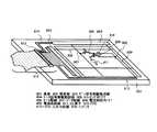
図1に本願発明のEL表示装置の回路構成を示す。図1(A)のEL表示装置は、基板
上に形成されたTFTによって画素部101、画素部の周辺に配置されたデータ信号側駆
動回路102及びゲート信号側駆動回路103を有している。
なお、本実施の形態でEL表示装置はデータ信号側駆動回路とゲート信号側駆動回路とを
1つづつ有しているが、本願発明においてデータ信号側駆動回路は2つあってもよい。ま
たゲート信号側駆動回路も2つあってもよい。FIG. 1 shows a circuit configuration of an EL display device of the present invention. The EL display device in FIG. 1A includes a pixel portion 101 by a TFT formed over a substrate, a data signal side driver circuit 102 and a gate signal side driver circuit 103 arranged around the pixel portion.
In this embodiment mode, the EL display device has one data signal side driving circuit and one gate signal side driving circuit. However, in the present invention, there may be two data signal side driving circuits. There may also be two gate signal side driving circuits.
データ信号側駆動回路102は基本的にシフトレジスタ102a、ラッチ(A)102b
、ラッチ(B)102cを含む。また、シフトレジスタ102aにはクロックパルス(CK
)及びスタートパルス(SP)が入力され、ラッチ(A)102bにはデジタルデータ信
号(Digital Data Signals)が入力され、ラッチ(B)102cにはラッチ信号(Latch S
ignals)が入力される。The data signal side driving circuit 102 basically includes a shift register 102a and a latch (A) 102b.
Latch (B) 102c. The shift register 102a has a clock pulse (CK
) And a start pulse (SP) are input, a digital data signal (Digital Data Signals) is input to the latch (A) 102b, and a latch signal (Latch S) is input to the latch (B) 102c.
ignals) is entered.
画素部に入力されるデジタルデータ信号は、時分割階調データ信号発生回路114にて
形成される。この回路ではアナログ信号又はデジタル信号でなるビデオ信号(画像情報を
含む信号)を、時分割階調を行うためのデジタルデータ信号に変換すると共に、時分割階
調表示を行うために必要なタイミングパルス等を発生させる回路である。A digital data signal input to the pixel portion is formed by the time division gradation data signal generation circuit 114. In this circuit, a video signal (a signal including image information) composed of an analog signal or a digital signal is converted into a digital data signal for performing time-division gradation, and a timing pulse necessary for performing time-division gradation display. And the like.
典型的には、時分割階調データ信号発生回路114には、1フレーム期間をnビット(
nは2以上の整数)の階調に対応した複数のサブフレーム期間に分割する手段と、それら
複数のサブフレーム期間においてアドレス期間及びサステイン期間を選択する手段と、そ
のサステイン期間をTs1:Ts2:Ts3:…:Ts(n-1):Ts(n)=20:2-1:2
-2:…:2-(n-2):2-(n-1)となるように設定する手段とが含まれる。Typically, the time-division gradation data signal generation circuit 114 has one frame period of n bits (
n is an integer of 2 or more) means for dividing into a plurality of subframe periods, means for selecting an address period and a sustain period in the plurality of subframe periods, and the sustain period as Ts1: Ts2: Ts3: ...: Ts (n-1): Ts (n) = 20 : 2-1 : 2
-2 : ...: 2-(n-2) : 2-(n-1) means for setting to be included.
この時分割階調データ信号発生回路114は、本願発明のEL表示装置の外部に設けら
れても良い。その場合、そこで形成されたデジタルデータ信号が本願発明のEL表示装置
に入力される構成となる。この場合、本願発明のEL表示装置をディスプレイとして有す
る電子装置は、本願発明のEL表示装置と時分割階調データ信号発生回路を別の部品とし
て含むことになる。The time-division gradation data signal generation circuit 114 may be provided outside the EL display device of the present invention. In that case, the digital data signal formed there is input to the EL display device of the present invention. In this case, an electronic device having the EL display device of the present invention as a display includes the EL display device of the present invention and a time-division gradation data signal generation circuit as separate components.
また、時分割階調データ信号発生回路114をICチップなどの形で本願発明のEL表
示装置に実装しても良い。その場合、そのICチップで形成されたデジタルデータ信号が
本願発明のEL表示装置に入力される構成となる。この場合、本願発明のEL表示装置を
ディスプレイとして有する電子装置は、時分割階調データ信号発生回路を含むICチップ
を実装した本願発明のEL表示装置を部品として含むことになる。Further, the time division gradation data signal generation circuit 114 may be mounted on the EL display device of the present invention in the form of an IC chip or the like. In that case, a digital data signal formed by the IC chip is input to the EL display device of the present invention. In this case, an electronic device having the EL display device of the present invention as a display includes the EL display device of the present invention on which an IC chip including a time division gradation data signal generation circuit is mounted as a component.
また最終的には、時分割階調データ信号発生回路114を画素部101、データ信号側
駆動回路102及びゲート信号側駆動回路103と同一の基板上にTFTでもって形成し
うる。この場合、EL表示装置に画像情報を含むビデオ信号を入力すれば全て基板上で処
理することができる。勿論、この場合の時分割階調データ信号発生回路は本願発明で用い
るポリシリコン膜を活性層とするTFTで形成することが望ましい。また、この場合、本
願発明のEL表示装置をディスプレイとして有する電子装置は、時分割階調データ信号発
生回路がEL表示装置自体に内蔵されており、電子装置の小型化を図ることが可能である
。Finally, the time-division gradation data signal generation circuit 114 can be formed with TFTs on the same substrate as the pixel portion 101, the data signal side driving circuit 102, and the gate signal side driving circuit 103. In this case, if a video signal including image information is input to the EL display device, all can be processed on the substrate. Of course, it is desirable that the time-division gradation data signal generation circuit in this case is formed of a TFT having a polysilicon film used in the present invention as an active layer. In this case, in the electronic device having the EL display device of the present invention as a display, the time-division gradation data signal generation circuit is built in the EL display device itself, and the electronic device can be miniaturized. .
画素部101にはマトリクス状に複数の画素104が配列される。画素104の拡大図
を図1(B)に示す。図1(B)において、105はスイッチング用TFTである。スイ
ッチング用TFT105のゲート電極は、ゲート信号を入力するゲート配線106に接続
されている。スイッチング用TFT105のソース領域とドレイン領域は、一方はデジタ
ルデータ信号を入力するデータ配線(ソース配線ともいう)107に接続されており、も
う一方はEL駆動用TFT108のゲート電極に接続されている。A plurality of
デジタルデータ信号は「0」または「1」の情報を有しており、「0」と「1」のデジ
タルデータ信号のうち、一方はHi、もう一方はLoの電位を有している。The digital data signal has information of “0” or “1”, and one of the digital data signals “0” and “1” has a potential of Hi and the other has a potential of Lo.
また、EL駆動用TFT108のソース領域は電源供給線111に接続され、ドレイン
領域はEL素子110に接続される。The source region of the
EL素子110はEL駆動用TFT108のドレイン領域に接続された画素電極と、E
L層を挟んで画素電極に対向して設けられた対向電極とでなり、対向電極は一定の電位(
コモン電位)に保たれているコモン電源112に接続されている。The
The counter electrode is provided so as to face the pixel electrode with the L layer interposed therebetween, and the counter electrode has a constant potential (
The
なおEL素子110の陽極を画素電極として用い、陰極を対向電極として用いる場合、
EL駆動用TFT108はpチャネル型TFTであることが好ましい。When the anode of the
The
なおEL素子110の陰極を画素電極として用い、陽極を対向電極として用いる場合、
EL駆動用TFT108はnチャネル型TFTであることが好ましい。When the cathode of the
The
電源供給線111にかかる電位をEL駆動電位と呼ぶ。EL素子が発光している時のE
L駆動電位をオンのEL駆動電位と呼ぶ。またEL素子が発光してない時のEL駆動電位
をオフのEL駆動電位と呼ぶ。A potential applied to the
The L drive potential is referred to as an ON EL drive potential. An EL drive potential when the EL element is not emitting light is referred to as an OFF EL drive potential.
そしてさらに、EL駆動電位とコモン電位との差をEL駆動電圧と呼ぶ。EL素子が発
光している時のEL駆動電圧をオンのEL駆動電圧と呼ぶ。またEL素子が発光してない
時のEL駆動電圧をオフのEL駆動電圧と呼ぶ。Further, the difference between the EL drive potential and the common potential is called an EL drive voltage. An EL drive voltage when the EL element emits light is referred to as an ON EL drive voltage. An EL drive voltage when the EL element is not emitting light is referred to as an OFF EL drive voltage.
電源供給線111にかかるオンのEL駆動電圧は、対応する画素の表示する色(赤色、
緑色、青色)によって、その値を変える。例えば用いる有機EL材料の赤色の発光輝度が
、青色と緑色の発光輝度よりも低い場合、赤色を表示する画素に接続されている電源供給
線にかかるオンのEL駆動電圧を、青色と緑色を表示する画素に接続されている電源供給
線にかかるオンのEL駆動電圧よりも大きく設定する。The ON EL drive voltage applied to the
The value is changed according to green and blue. For example, when the red light emission luminance of the organic EL material to be used is lower than the blue and green light emission luminances, the ON EL drive voltage applied to the power supply line connected to the pixel displaying red is displayed in blue and green. It is set to be larger than the ON EL drive voltage applied to the power supply line connected to the pixel.
なお、EL駆動用TFT108のドレイン領域と、EL素子110が有する画素電極と
の間に抵抗体を設けても良い。抵抗体を設けることによって、EL駆動用TFTからEL
素子へ供給される電流量を制御し、EL駆動用TFTの特性のバラツキの影響を防ぐこと
が可能になる。抵抗体はEL駆動用TFT108のオン抵抗よりも十分に大きい抵抗値を
示す素子であれば良いため、構造等に限定はない。なお、オン抵抗とは、TFTがオン状
態の時に、TFTのドレイン電圧をその時に流れているドレイン電流で割った値である。
抵抗体の抵抗値としては1kΩ〜50MΩ(好ましくは10kΩ〜10MΩ、さらに好ま
しくは50kΩ〜1MΩ)の範囲から選択すれば良い。抵抗体として抵抗値の高い半導体
層を用いると形成が容易であり好ましい。Note that a resistor may be provided between the drain region of the
By controlling the amount of current supplied to the element, it becomes possible to prevent the influence of variations in the characteristics of the EL driving TFT. Since the resistor may be an element having a resistance value sufficiently larger than the ON resistance of the
The resistance value of the resistor may be selected from the range of 1 kΩ to 50 MΩ (preferably 10 kΩ to 10 MΩ, more preferably 50 kΩ to 1 MΩ). A semiconductor layer having a high resistance value is preferably used as the resistor because it can be easily formed.
また、スイッチング用TFT105が非選択状態(オフ状態)にある時、EL駆動用T
FT108のゲート電圧を保持するためにコンデンサ113が設けられる。このコンデン
サ113はスイッチング用TFT105のドレイン領域と電源供給線111とに接続され
ている。When the switching
A
次に時分割階調表示について、図1及び図2を用いて説明する。ここではnビットデジ
タル駆動方式により2n階調の表示を行う場合について説明する。Next, time-division gradation display will be described with reference to FIGS. Here, a case where 2n gradation display is performed by the n-bit digital driving method will be described.
まず、1フレーム期間をn個のサブフレーム期間(SF1〜SFn)に分割する。なお
、画素部の全ての画素が1つの画像を表示する期間を1フレーム期間と呼ぶ。通常のEL
ディスプレイでは発振周波数は60Hz以上、即ち1秒間に60以上のフレーム期間が設
けられており、1秒間に60以上の画像が表示されている。1秒間に表示される画像の数
が60より少なくなると、視覚的にフリッカ等の画像のちらつきが目立ち始める。なお、
1フレーム期間をさらに複数に分割した期間をサブフレーム期間と呼ぶ。階調数が多くな
るにつれて1フレーム期間の分割数も増え、駆動回路を高い周波数で駆動しなければなら
ない。(図2)First, one frame period is divided into n subframe periods (SF1 to SFn). Note that a period in which all the pixels in the pixel portion display one image is referred to as one frame period. Normal EL
In the display, the oscillation frequency is 60 Hz or more, that is, 60 or more frame periods are provided per second, and 60 or more images are displayed per second. When the number of images displayed per second is less than 60, flickering of images such as flicker starts to be noticeable. In addition,
A period obtained by further dividing one frame period into a plurality is called a subframe period. As the number of gradations increases, the number of divisions in one frame period also increases, and the drive circuit must be driven at a high frequency. (Figure 2)
1つのサブフレーム期間はアドレス期間(Ta)とサステイン期間(Ts)とに分けら
れる。アドレス期間とは、1サブフレーム期間中、全画素にデータを入力するのに要する
時間であり、サステイン期間(点灯期間とも呼ぶ)とは、EL素子を発光させる期間を示
している。One subframe period is divided into an address period (Ta) and a sustain period (Ts). An address period is a time required to input data to all pixels in one subframe period, and a sustain period (also referred to as a lighting period) indicates a period during which an EL element emits light.
n個のサブフレーム期間(SF1〜SFn)がそれぞれ有するアドレス期間(Ta1〜
Tan)の長さは全て一定である。SF1〜SFnがそれぞれ有するサステイン期間(T
s)をそれぞれTs1〜Tsnとする。Each of the n subframe periods (SF1 to SFn) has an address period (Ta1 to Ta1).
The length of Tan) is all constant. Sustain period (T) each of SF1 to SFn has
Let s) be Ts1 to Tsn, respectively.
サステイン期間の長さは、Ts1:Ts2:Ts3:…:Ts(n−1):Tsn=20
:2-1:2-2:…:2-(n-2):2-(n-1)となるように設定する。但し、SF1〜SFnを
出現させる順序はどのようにしても良い。このサステイン期間の組み合わせで2n階調の
うち所望の階調表示を行うことができる。The length of the sustain period, Ts1: Ts2: Ts3: ... : Ts (n-1): Tsn = 2 0
: 2−1 :2-2 −2 :...: 2− (n−2) : 2− (n−1) . However, the order in which SF1 to SFn appear is not limited. A desired gradation display among 2n gradations can be performed by combining the sustain periods.
まず、電源供給線111がオフのEL駆動電位に保たれている状態にしておき、ゲート
配線106にゲート信号を印加し、ゲート配線106に接続されているスイッチング用T
FT105全てをON状態にする。なおオフのEL駆動電位は、EL素子が発光しない程
度にコモン電位と同じぐらいの電位である。First, the
All
そしてスイッチング用TFT105をON状態にした後、またはON状態にするのと同
時にスイッチング用TFT105のソース領域に「0」または「1」の情報を有するデジ
タルデータ信号を入力していく。Then, after the switching
デジタルデータ信号がスイッチング用TFT105を介してEL駆動用TFT108の
ゲート電極に接続されたコンデンサ113に入力され保持される。全ての画素にデジタル
データ信号が入力されるまでの期間がアドレス期間である。A digital data signal is input and held in the
アドレス期間が終了したら、電源供給線111がオンのEL駆動電位に保たれ、またス
イッチング用TFTがオフ状態になり、コンデンサ113において保持されたデジタルデ
ータ信号が、EL駆動用TFT108のゲート電極に入力される。When the address period ends, the
なお、オンのEL駆動電位の高さは、コモン電位との間にEL素子が発光する程度の電
位差を有する高さである。陽極にかかる電位は陰極にかかる電位よりも高いことがより望
ましい。つまり陽極を画素電極として用いる場合、オンのEL駆動電位はコモン電位より
も高いことが望ましい。逆に陰極を画素電極として用いる場合、オンのEL駆動電位はコ
モン電位よりも低いことが望ましい。Note that the height of the ON EL drive potential is a height having a potential difference with which the EL element emits light with respect to the common potential. More preferably, the potential applied to the anode is higher than the potential applied to the cathode. That is, when the anode is used as the pixel electrode, it is desirable that the ON EL driving potential be higher than the common potential. On the other hand, when the cathode is used as the pixel electrode, it is desirable that the ON EL drive potential be lower than the common potential.
本実施の形態において、デジタルデータ信号が「0」の情報を有していた場合、EL駆
動用TFT108はオフ状態となり、電源供給線111に印加されているオンのEL駆動
電圧はEL素子110が有する陽極(画素電極)に印加されない。In this embodiment, when the digital data signal has information of “0”, the
逆に、「1」の情報を有していた場合、EL駆動用TFT108はオン状態となり、電
源供給線111に印加されているオンのEL駆動電圧は、EL素子110が有する陽極(
画素電極)に印加される。On the other hand, when the information of “1” is included, the
Applied to the pixel electrode).
その結果、「0」の情報を有するデジタルデータ信号が印加された画素が有するEL素
子110は発光しない。そして「1」の情報を有するデジタルデータ信号が印加された画
素が有するEL素子110は発光する。発光が終了するまでの期間がサステイン期間であ
る。As a result, the
EL素子110を発光させる(画素を点灯させる)期間はTs1〜Tsnまでのいずれ
かの期間である。ここではTsnの期間、所定の画素を点灯させたとする。The period during which the
次に、再びアドレス期間に入り、全画素にデータ信号を入力したらサステイン期間に入
る。このときはTs1〜Ts(n−1)のいずれかの期間がサステイン期間となる。ここ
ではTs(n−1)の期間、所定の画素を点灯させたとする。Next, the address period starts again, and when a data signal is input to all pixels, the sustain period starts. At this time, any period from Ts1 to Ts (n-1) is a sustain period. Here, it is assumed that a predetermined pixel is lit for a period of Ts (n−1).
以下、残りのn−2個のサブフレームについて同様の動作を繰り返し、順次Ts(n−
2)、Ts(n−3)…Ts1とサステイン期間を設定し、それぞれのサブフレームで所
定の画素を点灯させたとする。Thereafter, the same operation is repeated for the remaining n-2 subframes, and sequentially Ts (n−
2), Ts (n−3)... Ts1 and the sustain period are set, and a predetermined pixel is turned on in each subframe.
n個のサブフレーム期間が出現したら1フレーム期間を終えたことになる。このとき、
画素が点灯していたサステイン期間、言い換えると「1」の情報を有するデジタルデータ
信号が画素に印加されたアドレス期間の直後のサステイン期間の長さを積算することによ
って、その画素の階調がきまる。例えば、n=8のとき、全部のサステイン期間で画素が
発光した場合の輝度を100%とすると、Ts1とTs2において画素が発光した場合に
は75%の輝度が表現でき、Ts3とTs5とTs8を選択した場合には16%の輝度が
表現できる。When n subframe periods appear, one frame period is finished. At this time,
The gradation of the pixel is determined by accumulating the length of the sustain period in which the pixel is lit, in other words, the length of the sustain period immediately after the address period in which the digital data signal having information “1” is applied to the pixel. . For example, when n = 8, assuming that the luminance is 100% when the pixels emit light in the entire sustain period, when the pixels emit light at Ts1 and Ts2, 75% luminance can be expressed, and Ts3, Ts5, and Ts8. When is selected, a luminance of 16% can be expressed.
そしてさらに本願発明では、電源供給線111にかかるオンのEL駆動電圧の値を、対
応する画素の表示する色(赤、緑、青)によって変えている。例えば用いる有機EL材料
の赤色の発光輝度が、青色と緑色の発光輝度よりも低い場合、赤色を表示する画素に接続
されている電源供給線にかかるオンのEL駆動電圧を、青色と緑色を表示する画素に接続
されている電源供給線にかかるオンのEL駆動電圧よりも大きくなるように設定する。Further, in the present invention, the value of the ON EL drive voltage applied to the
なお、オンのEL駆動電位の値を変えると同時に、デジタルデータ信号及びゲート信号
の有する電位の値を適宜変えることも重要である。Note that it is also important to appropriately change the values of the potentials of the digital data signal and the gate signal at the same time as changing the value of the ON EL drive potential.
次に本願発明における、EL駆動用TFTの構成について説明する。本願発明において
、EL駆動用TFTはpチャネル型TFTまたはnチャネル型TFTで構成される。pチ
ャネル型TFTで構成されるEL駆動用TFTはLDD領域を有さず、nチャネル型TF
Tで構成されるEL駆動用TFTはLDD領域を有す。Next, the configuration of the EL driving TFT in the present invention will be described. In the present invention, the EL driving TFT is composed of a p-channel TFT or an n-channel TFT. An EL driving TFT composed of a p-channel TFT does not have an LDD region, and an n-channel TF
The EL driving TFT composed of T has an LDD region.
EL駆動用TFTはスイッチング用TFTよりも、制御する電流の量が大きい。特に発
光輝度の低い色を表示する画素のEL駆動用TFTは、他の色を表示する画素のEL駆動
用TFTより制御する電流の量が大きい。The EL driving TFT has a larger amount of current to be controlled than the switching TFT. In particular, the EL driving TFT of a pixel that displays a color with low emission luminance has a larger amount of current to be controlled than the EL driving TFT of a pixel that displays another color.
EL駆動用TFTがpチャネル型TFTの場合、発光輝度の低い色を表示する画素のE
L駆動用TFTのチャネル幅(W)を、発光輝度の比較的高い色を表示する画素のEL駆
動用TFTのチャネル幅(W)より大きくする。上記構成によって、発光輝度の低い色を
表示する画素のEL駆動用TFTが、他の色を表示する画素のEL駆動用TFTより制御
する電流の量が大きくても、発光輝度の低い色を表示する画素のEL駆動用TFTがホッ
トキャリア注入によって早く劣化してしまうのを防ぐことができる。When the EL driving TFT is a p-channel TFT, the E of the pixel displaying a color with low emission luminance
The channel width (W) of the L driving TFT is made larger than the channel width (W) of the EL driving TFT of the pixel displaying a color with relatively high light emission luminance. With the above configuration, the EL driving TFT of a pixel displaying a color with low emission luminance displays a color with low emission luminance even if the amount of current controlled is larger than the EL driving TFT of a pixel displaying another color. It is possible to prevent the EL driving TFT of the pixel to be deteriorated quickly by hot carrier injection.
EL駆動用TFTがnチャネル型TFTの場合も、発光輝度の低い色を表示する画素の
EL駆動用TFTのチャネル幅(W)を、発光輝度の比較的高い色を表示する画素のEL
駆動用TFTのチャネル幅(W)より大きくすることで、発光輝度の低い色を表示する画
素のEL駆動用TFTがホットキャリア注入によって早く劣化してしまうのを防ぐことが
可能である。Even when the EL driving TFT is an n-channel TFT, the channel width (W) of the EL driving TFT of the pixel that displays a color with low emission luminance is set to the EL of the pixel that displays a color with relatively high emission luminance.
By making it larger than the channel width (W) of the driving TFT, it is possible to prevent the EL driving TFT of a pixel displaying a color with low emission luminance from deteriorating rapidly due to hot carrier injection.
EL駆動用TFTがnチャネル型TFTの場合、上記構成を有さなくとも、発光輝度の
低い色を表示する画素のEL駆動用TFTのLDD領域の長さを、発光輝度の比較的高い
色を表示する画素のEL駆動用TFTのLDD領域の長さより長くすることで、発光輝度
の低い色を表示する画素のEL駆動用TFTがホットキャリア注入により劣化するのを防
ぐことができる。EL駆動用TFTがnチャネル型TFTの場合、上記したような、画素
によってEL駆動用TFTのチャネル幅(W)を異ならせる構成と、画素によってEL駆
動用TFTのLDD領域の長さを異ならせる構成とを両方有していても良い。When the EL driving TFT is an n-channel TFT, the length of the LDD region of the EL driving TFT of a pixel that displays a color with low emission luminance is set to a color with relatively high emission luminance without having the above configuration. By making it longer than the length of the LDD region of the EL driving TFT of the pixel to be displayed, it is possible to prevent the EL driving TFT of the pixel displaying a color with low emission luminance from being deteriorated by hot carrier injection. In the case where the EL driving TFT is an n-channel TFT, the configuration in which the channel width (W) of the EL driving TFT is different depending on the pixel as described above, and the length of the LDD region of the EL driving TFT is different depending on the pixel. You may have both a structure.
本願発明は上記構成により、EL素子に印加されるオンのEL駆動電位の値によって、
目的とする画素の有するEL素子の発光輝度を調節することが可能になり、赤色、青色、
緑色の発光輝度のバランスが良い、色鮮やかな画像を表示することができる。そしてなお
かつ、オンのEL駆動電圧が大きくなることによってEL駆動用TFTが制御する電流の
量が増えても、EL駆動用TFTの劣化を抑えることができる。The present invention has the above-described configuration, and the value of the ON EL drive potential applied to the EL element
It becomes possible to adjust the light emission luminance of the EL element of the target pixel, red, blue,
It is possible to display a colorful image with a good balance of green emission luminance. In addition, even if the amount of current controlled by the EL driving TFT is increased by increasing the ON EL driving voltage, the deterioration of the EL driving TFT can be suppressed.
なおかつ本願発明は時分割階調表示によって鮮明な多階調表示を行うことが可能になる
。そしてなおかつ、印加される電圧が高くなることによってEL駆動用TFTが制御する
電流の量が増えても、EL駆動用TFTの劣化を抑えることができる。In addition, the present invention can perform clear multi-gradation display by time-division gradation display. In addition, even when the amount of current controlled by the EL driving TFT is increased by increasing the applied voltage, deterioration of the EL driving TFT can be suppressed.
本実施例では8ビットデジタル駆動方式により256階調(1677万色)のフルカラ
ー表示を行う場合の時分割階調表示について説明する。本実施例において、は赤色の発光
輝度が青色と緑色の発光輝度よりも低い有機EL材料を用いたEL表示装置の駆動につい
て説明する。In this embodiment, time-division gradation display when full-color display of 256 gradations (16.77 million colors) is performed by an 8-bit digital drive method will be described. In this embodiment, driving of an EL display device using an organic EL material whose red emission luminance is lower than that of blue and green will be described.
まず、1フレーム期間を8個のサブフレーム期間(SF1〜SF8)に分割する。本実
施例のEL表示装置では、発振周波数は60Hzとし、1秒間に60のフレーム期間が設
けられており、1秒間に60の画像が表示される。(図3)First, one frame period is divided into eight subframe periods (SF1 to SF8). In the EL display device of this embodiment, the oscillation frequency is 60 Hz, 60 frame periods are provided per second, and 60 images are displayed per second. (Figure 3)
1つのサブフレーム期間はアドレス期間(Ta)とサステイン期間(Ts)とに分けら
れる。SF1〜SF8がそれぞれ有するアドレス期間(Ta1〜Ta8)の長さは全て一
定である。SF1〜SF8がそれぞれ有するサステイン期間(Ts)をそれぞれTs1〜
Ts8とする。One subframe period is divided into an address period (Ta) and a sustain period (Ts). The lengths of the address periods (Ta1 to Ta8) included in SF1 to SF8 are all constant. Each of the sustain periods (Ts) of SF1 to SF8 has Ts1 to Ts1.
Let Ts8.
サステイン期間の長さは、Ts1:Ts2:Ts3:Ts4:Ts5:Ts6:Ts7
:Ts8=1:1/2:1/4:1/8:1/16:1/32:1/64:1/128と
なるように設定する。但し、SF1〜SF8を出現させる順序はどのようにしても良い。
このサステイン期間の組み合わせで256階調のうち所望の階調表示を行うことができる
。The length of the sustain period is Ts1: Ts2: Ts3: Ts4: Ts5: Ts6: Ts7
: Ts8 = 1: 1/2: 1/4: 1/8: 1/16: 1/32: 1/64: 1/128. However, the order in which SF1 to SF8 appear may be any way.
A desired gradation display among 256 gradations can be performed by combining the sustain periods.
まず、電源供給線がオフのEL駆動電位に保たれている状態にしておき、ゲート配線に
ゲート信号を印加し、ゲート配線に接続されているスイッチング用TFT全てをON状態
にする。本実施例ではオフのEL駆動電位を0Vとする。なお、本実施例では、EL素子
の陽極を画素電極として電源供給線に接続しており、陰極を対向電極としてコモン電源に
接続している。First, the power supply line is kept in the off EL drive potential, a gate signal is applied to the gate wiring, and all the switching TFTs connected to the gate wiring are turned on. In this embodiment, the off EL drive potential is set to 0V. In this embodiment, the anode of the EL element is connected to the power supply line as a pixel electrode, and the cathode is connected to a common power supply as a counter electrode.
そしてスイッチング用TFTをON状態にした後、またはON状態にするのと同時にス
イッチング用TFTのソース領域に「0」または「1」の情報を有するデジタルデータ信
号を入力していく。Then, after the switching TFT is turned on or at the same time as being turned on, a digital data signal having information of “0” or “1” is input to the source region of the switching TFT.
デジタルデータ信号がスイッチング用TFTを介して、EL駆動用TFTのゲート電極
に接続されたコンデンサに入力され保持される。全ての画素にデジタルデータ信号が入力
されるまでの期間がアドレス期間である。The digital data signal is input and held in the capacitor connected to the gate electrode of the EL driving TFT via the switching TFT. The period until the digital data signal is input to all the pixels is the address period.
アドレス期間が終了したら、電源供給線がオンのEL駆動電位に保たれ、またスイッチ
ング用TFTがオフ状態になり、コンデンサにおいて保持されたデジタルデータ信号が、
EL駆動用TFTのゲート電極に入力される。本実施例では、サステイン期間において、
赤色の表示用の画素に接続された電源供給線は10VのオンのEL駆動電位に保たれる。
また緑色と青色の表示用の画素に接続された電源供給線は5VのオンのEL駆動電位に保
たれる。When the address period ends, the power supply line is kept at the ON EL drive potential, the switching TFT is turned off, and the digital data signal held in the capacitor is
Input to the gate electrode of the EL driving TFT. In this example, in the sustain period,
The power supply line connected to the red display pixel is kept at an ON EL drive potential of 10V.
The power supply line connected to the display pixels for green and blue is kept at an EL drive potential of 5V.
本実施例において、デジタルデータ信号が「0」の情報を有していた場合、EL駆動用
TFTはオフ状態となり、電源供給線に印加されているオンのEL駆動電圧はEL素子が
有する陽極(画素電極)に印加されない。In this embodiment, when the digital data signal has information of “0”, the EL driving TFT is turned off, and the ON EL driving voltage applied to the power supply line is the anode ( Not applied to the pixel electrode).
逆に、「1」の情報を有していた場合、EL駆動用TFTはオン状態となり、電源供給
線に印加されているオンのEL駆動電圧は、EL素子が有する陽極(画素電極)に印加さ
れる。On the other hand, when the information “1” is included, the EL driving TFT is turned on, and the ON EL driving voltage applied to the power supply line is applied to the anode (pixel electrode) of the EL element. Is done.
その結果、「0」の情報を有するデジタルデータ信号が印加された画素が有するEL素
子は発光しない。そして「1」の情報を有するデジタルデータ信号が印加された画素が有
するEL素子は発光する。発光が終了するまでの期間がサステイン期間である。As a result, the EL element included in the pixel to which the digital data signal having the information “0” is applied does not emit light. The EL element included in the pixel to which the digital data signal having the information “1” is applied emits light. The period until the light emission ends is the sustain period.
ELを発光させる(画素を点灯させる)期間はTs1〜Ts8までのいずれかの期間で
ある。ここではTs8の期間、所定の画素を点灯させたとする。The period during which EL is emitted (pixels are lit) is any period from Ts1 to Ts8. Here, it is assumed that a predetermined pixel is lit for a period of Ts8.
次に、再びアドレス期間に入り、全画素にデータ信号を入力したらサステイン期間に入
る。このときはTs1〜Ts7のいずれかの期間がサステイン期間となる。ここではTs
7の期間、所定の画素を点灯させたとする。Next, the address period starts again, and when a data signal is input to all pixels, the sustain period starts. At this time, one of the periods Ts1 to Ts7 is a sustain period. Here Ts
Assume that a predetermined pixel is lit for 7 periods.
以下、残りの6つのサブフレームについて同様の動作を繰り返し、順次Ts6、Ts5
…Ts1とサステイン期間を設定し、それぞれのサブフレームで所定の画素を点灯させた
とする。Thereafter, the same operation is repeated for the remaining six subframes, and sequentially Ts6, Ts5
... Ts1 and the sustain period are set, and a predetermined pixel is turned on in each subframe.
8つのサブフレーム期間が出現したら1フレーム期間を終えたことになる。このとき、
画素が点灯したサステイン期間、言い換えると「1」の情報を有するデジタルデータ信号
が画素に印加されたアドレス期間の直後のサステイン期間の長さを積算することによって
、その画素の階調が決まる。例えば、全部のサステイン期間で画素が発光した場合の輝度
を100%とすると、Ts1とTs2において画素が発光した場合には75%の輝度が表
現でき、Ts3とTs5とTs8を選択した場合には16%の輝度が表現できる。When eight subframe periods appear, one frame period is finished. At this time,
The gradation of the pixel is determined by integrating the length of the sustain period immediately after the address period in which the digital data signal having the information “1” is applied to the pixel. For example, if the luminance is 100% when the pixels emit light during the entire sustain period, 75% luminance can be expressed when the pixels emit light at Ts1 and Ts2, and when Ts3, Ts5, and Ts8 are selected. A luminance of 16% can be expressed.
なお、EL駆動電位の値を変えると同時に、デジタルデータ信号及びゲート信号の有す
る電位の値を適宜変えることも重要である。Note that it is also important to change the values of the potentials of the digital data signal and the gate signal at the same time as changing the value of the EL drive potential.
上記構成によって、本願発明はEL素子に印加するEL駆動電圧の値によって、目的と
する画素の有するEL素子の発光輝度を調節することが可能になり、なおかつ、時分割階
調表示によって鮮明な多階調表示を行うことが可能になった。
具体的には赤色の発光輝度が青色と緑色の発光輝度よりも低い有機EL材料を用いたEL
素子の、赤色、青色、緑色の発光輝度のバランスが良くなり、色鮮やかな画像を表示する
ことが可能になる。またなおかつ、デジタル信号により時分割階調表示を行い、EL駆動
用TFTの特性バラツキによる階調不良のない、色再現性の良い高精細な画像を得ること
ができる。With the above structure, the present invention makes it possible to adjust the light emission luminance of the EL element of the target pixel according to the value of the EL drive voltage applied to the EL element, and to display a clear image by time-division gradation display. It became possible to perform gradation display.
Specifically, an EL using an organic EL material whose red luminance is lower than that of blue and green
The red, blue, and green light emission luminance balance of the element is improved, and a colorful image can be displayed. In addition, time-division gradation display is performed with a digital signal, and a high-definition image with good color reproducibility without gradation defects due to variations in characteristics of the EL driving TFT can be obtained.
次に、本願発明のEL表示装置について、その断面構造の概略を図4を用いて説明する
。なお本実施例ではEL素子の陰極がEL駆動用TFTのドレイン領域に接続されている
例について説明する。Next, the outline of the cross-sectional structure of the EL display device of the present invention will be described with reference to FIG. In this embodiment, an example in which the cathode of the EL element is connected to the drain region of the EL driving TFT will be described.
図4において、11は基板、12は下地となる絶縁膜(以下、下地膜という)
である。基板11としては透光性基板、代表的にはガラス基板、石英基板、ガラスセラミ
ックス基板、又は結晶化ガラス基板を用いることができる。但し、作製プロセス中の最高
処理温度に耐えるものでなくてはならない。In FIG. 4, 11 is a substrate, 12 is an insulating film as a base (hereinafter referred to as a base film).
It is. As the
また、下地膜12は特に可動イオンを含む基板や導電性を有する基板を用いる場合に有
効であるが、石英基板には設けなくても構わない。下地膜12としては、珪素(シリコン
)を含む絶縁膜を用いれば良い。なお、本明細書において「珪素を含む絶縁膜」とは、具
体的には酸化珪素膜、窒化珪素膜若しくは窒化酸化珪素膜(SiOxNy:x、yは任意
の整数、で示される)など珪素に対して酸素若しくは窒素を所定の割合で含ませた絶縁膜
を指す。The
201はスイッチング用TFT、202はEL駆動用TFTであり、共にnチャネル型
TFTで形成されている。本願発明において、スイッチング用TFTとEL駆動用TFT
は、nチャネル型TFTでもpチャネル型TFTでも、どちらでも構わない。Reference numeral 201 denotes a switching TFT, and 202 denotes an EL driving TFT, both of which are formed by n-channel TFTs. In the present invention, switching TFT and EL driving TFT
Either an n-channel TFT or a p-channel TFT may be used.
ただしnチャネル型TFTの電界効果移動度はpチャネル型TFTの電界効果移動度よ
りも大きいため、動作速度が早く大電流を流しやすい。また、同じ電流量を流すにもTF
Tサイズはnチャネル型TFTの方が小さくできる。そのため、nチャネル型TFTをE
L駆動用TFTとして用いた方が画像表示部の有効発光面積が広くなるのでより好ましい
。However, since the field effect mobility of the n-channel TFT is larger than that of the p-channel TFT, the operation speed is high and a large current is likely to flow. Also, TF can be used for the same amount of current.
The T size can be made smaller for the n-channel TFT. Therefore, n-channel TFTs are
It is more preferable to use it as the L driving TFT because the effective light emitting area of the image display portion is widened.
スイッチング用TFT201は、ソース領域13、ドレイン領域14、LDD領域15
a〜15d、分離領域16及びチャネル形成領域17a、17bを含む活性層と、ゲート絶縁
膜18と、ゲート電極19a、19bと、第1層間絶縁膜20と、ソース配線21と、ドレ
イン配線22とを有している。なお、ゲート絶縁膜18又は第1層間絶縁膜20は基板上
の全TFTに共通であっても良いし、回路又は素子に応じて異ならせても良い。The switching TFT 201 includes a
active layers including a to 15d,
また、図4に示すスイッチング用TFT201はゲート電極19a、19bが電気的に接
続されており、いわゆるダブルゲート構造となっている。勿論、ダブルゲート構造だけで
なく、トリプルゲート構造などいわゆるマルチゲート構造(直列に接続された二つ以上の
チャネル形成領域を有する活性層を含む構造)であっても良い。Further, the switching TFT 201 shown in FIG. 4 has a so-called double gate structure in which the
マルチゲート構造はオフ電流を低減する上で極めて有効であり、スイッチング用TFT
のオフ電流を十分に低くすれば、それだけEL駆動用TFT202のゲート電極に接続さ
れたコンデンサが必要とする最低限の容量を抑えることができる。即ち、コンデンサの面
積を小さくすることができるので、マルチゲート構造とすることはEL素子の有効発光面
積を広げる上でも有効である。Multi-gate structure is extremely effective in reducing off current, and switching TFT
If the off-state current is sufficiently low, the minimum capacitance required by the capacitor connected to the gate electrode of the EL driving TFT 202 can be suppressed. That is, since the area of the capacitor can be reduced, the multi-gate structure is also effective in expanding the effective light emitting area of the EL element.
さらに、スイッチング用TFT201においては、LDD領域15a〜15dは、ゲート
絶縁膜18を介してゲート電極17a、17bと重ならないように設ける。このような構造
はオフ電流を低減する上で非常に効果的である。また、LDD領域15a〜15dの長さ(
幅)は0.5〜3.5μm、代表的には2.0〜2.5μmとすれば良い。Further, in the switching TFT 201, the
The width) may be 0.5 to 3.5 μm, typically 2.0 to 2.5 μm.
なお、チャネル形成領域とLDD領域との間にオフセット領域(チャネル形成領域と同
一組成の半導体層でなり、ゲート電圧が印加されない領域)を設けることはオフ電流を下
げる上でさらに好ましい。また、二つ以上のゲート電極を有するマルチゲート構造の場合
、チャネル形成領域の間に設けられた分離領域16(ソース領域又はドレイン領域と同一
の濃度で同一の不純物元素が添加された領域)がオフ電流の低減に効果的である。Note that it is more preferable to provide an offset region (a region including a semiconductor layer having the same composition as the channel formation region and to which no gate voltage is applied) between the channel formation region and the LDD region in order to reduce off-state current. In the case of a multi-gate structure having two or more gate electrodes, an isolation region 16 (a region to which the same impurity element is added at the same concentration as the source region or the drain region) provided between the channel formation regions is provided. It is effective for reducing the off current.
次に、EL駆動用TFT202は、ソース領域26、ドレイン領域27、LDD領域2
8及びチャネル形成領域29を含む活性層と、ゲート絶縁膜18と、ゲート電極30と、
第1層間絶縁膜20と、ソース配線31並びにドレイン配線32を有して形成される。本
実施例においてEL駆動用TFT202はnチャネル型TFTである。Next, the EL driving TFT 202 includes the
8 and the
The first interlayer insulating film 20, the
また、スイッチング用TFT201のドレイン領域14はEL駆動用TFT202のゲ
ート電極30に接続されている。図示してはいないが、具体的にはEL駆動用TFT20
2のゲート電極30はスイッチング用TFT201のドレイン領域14とドレイン配線(
接続配線とも言える)22を介して電気的に接続されている。なお、ゲート電極30はシ
ングルゲート構造となっているが、マルチゲート構造であっても良い。また、EL駆動用
TFT202のソース配線31は電源供給線(図示せず)に接続される。The
The
It is electrically connected via 22). The
EL駆動用TFT202はEL素子に注入される電流量を制御するための素子であり、
比較的多くの電流が流れる。そのため、チャネル幅(W)はスイッチング用TFTのチャ
ネル幅よりも大きく設計することが好ましい。また、EL駆動用TFT202に過剰な電
流が流れないように、チャネル長(L)は長めに設計することが好ましい。望ましくは一
画素あたり0.5〜2μA(好ましくは1〜1.5μA)となるようにする。The EL driving TFT 202 is an element for controlling the amount of current injected into the EL element.
A relatively large amount of current flows. Therefore, it is preferable to design the channel width (W) to be larger than the channel width of the switching TFT. Further, it is preferable that the channel length (L) is designed to be long so that excessive current does not flow through the EL driving TFT 202. Desirably, it is set to 0.5 to 2 μA (preferably 1 to 1.5 μA) per pixel.
特に本願発明においては、発光輝度の低い色を表示する画素のEL駆動用TFTには、
他の色を表示する画素のEL駆動用TFTよりも、制御する電流が大きい。そのため発光
輝度の低い色を表示する画素のEL駆動用TFTは、他の色を表示する画素のEL駆動用
TFTよりもホットキャリア注入によって早く劣化してしまう。In particular, in the present invention, the EL driving TFT of the pixel displaying a color with low emission luminance includes
The current to be controlled is larger than the EL driving TFT of the pixel displaying other colors. For this reason, the EL driving TFT of a pixel that displays a color with low emission luminance is deteriorated earlier by hot carrier injection than the EL driving TFT of a pixel that displays another color.
そのため本願発明では、発光輝度の低い色を表示する画素のEL駆動用TFTのLDD
領域の長さを、発光輝度の比較的高い色を表示する画素のEL駆動用TFTのLDD領域
の長さより長くした。これによって、EL駆動用TFTが制御する電流の量が増えること
によって、EL駆動用TFTが劣化するのを抑えることが可能になった。Therefore, in the present invention, the LDD of the EL driving TFT of the pixel that displays a color with low emission luminance.
The length of the region is longer than the length of the LDD region of the EL driving TFT of the pixel that displays a color with relatively high luminance. As a result, it is possible to suppress deterioration of the EL driving TFT due to an increase in the amount of current controlled by the EL driving TFT.
またさらに、EL駆動用TFT202の活性層(特にチャネル形成領域)の膜厚を厚く
する(好ましくは50〜100nm、さらに好ましくは60〜80nm)ことによって、
TFTの劣化を抑えてもよい。逆に、スイッチング用TFT201の場合はオフ電流を小
さくするという観点から見れば、活性層(特にチャネル形成領域)の膜厚を薄くする(好
ましくは20〜50nm、さらに好ましくは25〜40nm)ことも有効である。Furthermore, by increasing the film thickness of the active layer (particularly the channel formation region) of the EL driving TFT 202 (preferably 50 to 100 nm, more preferably 60 to 80 nm),
The deterioration of the TFT may be suppressed. On the contrary, in the case of the switching TFT 201, from the viewpoint of reducing the off-state current, the thickness of the active layer (especially the channel formation region) may be reduced (preferably 20 to 50 nm, more preferably 25 to 40 nm). It is valid.
以上は画素内に設けられたTFTの構造について説明したが、このとき同時に駆動回路
も形成される。図4には駆動回路を形成する基本単位となるCMOS回路が図示されてい
る。Although the above has described the structure of the TFT provided in the pixel, a driving circuit is also formed at this time. FIG. 4 shows a CMOS circuit as a basic unit for forming a driving circuit.
図4においては極力動作速度を落とさないようにしつつホットキャリア注入を低減させ
る構造を有するTFTをCMOS回路のnチャネル型TFT204として用いる。なお、
ここでいう駆動回路としては、データ信号側駆動回路、ゲート信号側駆動回路を指す。勿
論、他の論理回路(レベルシフタ、A/Dコンバータ、信号分割回路等)を形成すること
も可能である。In FIG. 4, a TFT having a structure for reducing hot carrier injection while reducing the operating speed as much as possible is used as the n-channel TFT 204 of the CMOS circuit. In addition,
The driving circuit here refers to a data signal side driving circuit and a gate signal side driving circuit. Of course, other logic circuits (level shifter, A / D converter, signal dividing circuit, etc.) can be formed.
CMOS回路のnチャネル型TFT204の活性層は、ソース領域35、ドレイン領域
36、LDD領域37及びチャネル形成領域38を含み、LDD領域37はゲート絶縁膜
18を介してゲート電極39と重なっている。The active layer of the n-channel TFT 204 in the CMOS circuit includes a
ドレイン領域36側のみにLDD領域37を形成しているのは、動作速度を落とさない
ための配慮である。また、このnチャネル型TFT204はオフ電流値をあまり気にする
必要はなく、それよりも動作速度を重視した方が良い。従って、LDD領域37は完全に
ゲート電極に重ねてしまい、極力抵抗成分を少なくすることが望ましい。即ち、いわゆる
オフセットはなくした方がよい。The reason why the
また、CMOS回路のpチャネル型TFT205は、ホットキャリア注入による劣化が
殆ど気にならないので、特にLDD領域を設けなくても良い。従って活性層はソース領域
40、ドレイン領域41及びチャネル形成領域42を含み、その上にはゲート絶縁膜18
とゲート電極43が設けられる。勿論、nチャネル型TFT204と同様にLDD領域を
設け、ホットキャリア対策を講じることも可能である。In addition, since the p-channel TFT 205 of the CMOS circuit is hardly concerned with deterioration due to hot carrier injection, it is not particularly necessary to provide an LDD region. Therefore, the active layer includes the
And a
また、nチャネル型TFT204及びpチャネル型TFT205はそれぞれソース領域
上に第1層間絶縁膜20を間に介して、ソース配線44、45を有している。また、ドレ
イン配線46によってnチャネル型TFT204とpチャネル型TFT205とのドレイ
ン領域は互いに電気的に接続される。Each of the n-channel TFT 204 and the p-channel TFT 205 has source wirings 44 and 45 on the source region with the first interlayer insulating film 20 interposed therebetween. Further, the drain regions of the n-channel TFT 204 and the p-channel TFT 205 are electrically connected to each other by the
次に、47は第1パッシベーション膜であり、膜厚は10nm〜1μm(好ましくは2
00〜500nm)とすれば良い。材料としては、珪素を含む絶縁膜(特に窒化酸化珪素
膜又は窒化珪素膜が好ましい)を用いることができる。このパッシベーション膜47は形
成されたTFTをアルカリ金属や水分から保護する役割金属を有する。最終的にTFT(
特にEL駆動用TFT)の上方に設けられるEL層にはナトリウム等のアルカリ金属が含
まれている。即ち、第1パッシベーション膜47はこれらのアルカリ金属(可動イオン)
をTFT側に侵入させない保護層としても働く。Next,
(00 to 500 nm). As a material, an insulating film containing silicon (in particular, a silicon nitride oxide film or a silicon nitride film is preferable) can be used. The
In particular, the EL layer provided above the EL driving TFT) contains an alkali metal such as sodium. That is, the
It also functions as a protective layer that does not enter the TFT side.
また、48は第2層間絶縁膜であり、TFTによってできる段差の平坦化を行う平坦化
膜としての機能を有する。第2層間絶縁膜48としては、有機樹脂膜が好ましく、ポリイ
ミド、ポリアミド、アクリル、BCB(ベンゾシクロブテン)
等を用いると良い。これらの有機樹脂膜は良好な平坦面を形成しやすく、比誘電率が低い
という利点を有する。EL層は凹凸に非常に敏感であるため、TFTによる段差は第2層
間絶縁膜で殆ど吸収してしまうことが望ましい。また、ゲート配線やデータ配線とEL素
子の陰極との間に形成される寄生容量を低減する上で、比誘電率の低い材料を厚く設けて
おくことが望ましい。従って、膜厚は0.5〜5μm(好ましくは1.5〜2.5μm)が
好ましい。
Etc. may be used. These organic resin films have an advantage that they can easily form a good flat surface and have a low relative dielectric constant. Since the EL layer is very sensitive to unevenness, it is desirable that the step due to the TFT is almost absorbed by the second interlayer insulating film. Further, in order to reduce the parasitic capacitance formed between the gate wiring or the data wiring and the cathode of the EL element, it is desirable to provide a thick material having a low relative dielectric constant. Therefore, the film thickness is preferably 0.5 to 5 μm (preferably 1.5 to 2.5 μm).
また、49は保護電極であり、各画素の画素電極51を接続するための電極である。保
護電極49としては、アルミニウム(Al)、銅(Cu)若しくは銀(Ag)を含む低抵
抗な材料を用いることが好ましい。この保護電極49にはEL層の発熱を緩和する放熱効
果も期待できる。保護電極49は、EL駆動用TFT202のドレイン配線32に接続さ
れるように形成される。
保護電極49の上には酸化珪素膜、窒化酸化珪素膜または有機樹脂膜でなる第3層間絶
縁膜50が0.3〜1μmの厚さに設けられる。この第3層間絶縁膜50は保護電極49
の上にエッチングにより開口部が設けられ、その開口部の縁はテーパー形状となるように
エッチングする。テーパーの角度は10〜60°(好ましくは30〜50°)とすると良
い。A third
An opening is provided on the upper portion by etching, and the edge of the opening is etched so as to have a tapered shape. The taper angle may be 10 to 60 ° (preferably 30 to 50 °).
第3層間絶縁膜50の上には画素電極(EL素子の陰極)51が設けられる。
陰極51としては、仕事関数の小さいマグネシウム(Mg)、リチウム(Li)
若しくはカルシウム(Ca)を含む材料を用いる。好ましくはMgAg(MgとAgをM
g:Ag=10:1で混合した材料)でなる電極を用いれば良い。他にもMgAgAl電
極、LiAl電極、また、LiFAl電極が挙げられる。A pixel electrode (cathode of EL element) 51 is provided on the third
As the
Alternatively, a material containing calcium (Ca) is used. MgAg (Mg and Ag are preferably M
g: a material mixed with Ag = 10: 1) may be used. Other examples include MgAgAl electrodes, LiAl electrodes, and LiFAl electrodes.
画素電極51の上にはEL層52が設けられる。EL層52は単層又は積層構造で用い
られるが、積層構造で用いた方が発光効率は良い。一般的には画素電極上に正孔注入層/
正孔輸送層/発光層/電子輸送層の順に形成されるが、正孔輸送層/発光層/電子輸送層
、または正孔注入層/正孔輸送層/発光層/電子輸送層/電子注入層のような構造でも良
い。本願発明では公知のいずれの構造を用いても良いし、EL層に対して蛍光性色素等を
ドーピングしても良い。An
The hole transport layer / light-emitting layer / electron transport layer is formed in this order, but the hole transport layer / light-emitting layer / electron transport layer or hole injection layer / hole transport layer / light-emitting layer / electron transport layer / electron injection A structure like a layer may be used. In the present invention, any known structure may be used, and the EL layer may be doped with a fluorescent dye or the like.
なお、EL表示装置には大きく分けて四つのカラー化表示方式があり、R(赤)G(緑
)B(青)に対応した三種類のEL素子を形成する方式、白色発光のEL素子とカラーフ
ィルターを組み合わせた方式、青色又は青緑発光のEL素子と蛍光体(蛍光性の色変換層
:CCM)とを組み合わせた方式、陰極(対向電極)
に透明電極を使用してRGBに対応したEL素子を重ねる方式、がある。The EL display device can be roughly divided into four color display methods, a method of forming three types of EL elements corresponding to R (red), G (green), and B (blue), a white light emitting EL element, and A combination of color filters, a combination of blue or blue-green light emitting elements and phosphors (fluorescent color conversion layer: CCM), cathode (counter electrode)
There is a method in which EL elements corresponding to RGB are stacked using transparent electrodes.
図4の構造はRGBに対応した三種類のEL素子を形成する方式を用いた場合の例であ
る。なお、図4には一つの画素しか図示していないが、同一構造の画素が赤、緑又は青の
それぞれの色に対応して形成され、これによりカラー表示を行うことができる。The structure of FIG. 4 is an example in the case of using a method of forming three types of EL elements corresponding to RGB. Although only one pixel is shown in FIG. 4, pixels having the same structure are formed corresponding to the respective colors of red, green, and blue, so that color display can be performed.
本願発明は発光方式に関わらず実施することが可能であり、上記四つの全ての方式を本
願発明に用いることができる。しかし、蛍光体はELに比べて応答速度が遅く残光が問題
となりうるので、蛍光体を用いない方式が望ましい。The present invention can be implemented regardless of the light emission method, and all the above four methods can be used in the present invention. However, since phosphors have a slower response speed than EL and afterglow can be a problem, a method that does not use phosphors is desirable.
次に透明導電膜でなる対向電極(EL素子の陽極)53をEL層上に形成する。本実施
例では、透明導電膜としてITO(Indium Tin Oxide)を用いた。Next, a counter electrode (anode of the EL element) 53 made of a transparent conductive film is formed on the EL layer. In this example, ITO (Indium Tin Oxide) was used as the transparent conductive film.
EL層52と対向電極53でなる積層体は、各画素で個別に形成する必要があるが、E
L層52は水分に極めて弱いため、通常のフォトリソグラフィ技術を用いることができな
い。従って、メタルマスク等の物理的なマスク材を用い、真空蒸着法、スパッタ法、プラ
ズマCVD法等の気相法で選択的に形成することが好ましい。A laminate including the
Since the
なお、EL層を選択的に形成する方法として、インクジェット法、スクリーン印刷法又
はスピンコート法等を用いることも可能である。Note that an ink-jet method, a screen printing method, a spin coating method, or the like can be used as a method for selectively forming the EL layer.
また、54は第2パッシベーション膜であり、膜厚は10nm〜1μm(好ましくは2
00〜500nm)とすれば良い。第2パッシベーション膜54を設けるのは、EL層5
2を水分から保護する目的が主であるが、放熱効果をもたせることも有効である。但し、
上述のようにEL層は熱に弱いので、なるべく低温(好ましくは室温から120℃までの
温度範囲)で成膜するのが望ましい。従って、プラズマCVD法、スパッタ法、真空蒸着
法、イオンプレーティング法又は溶液塗布法(スピンコーティング法)が望ましい成膜方
法と言える。
(00 to 500 nm). The
The main purpose is to protect 2 from moisture, but it is also effective to have a heat dissipation effect. However,
Since the EL layer is vulnerable to heat as described above, it is desirable to form the film at as low a temperature as possible (preferably in a temperature range from room temperature to 120 ° C.). Therefore, the plasma CVD method, the sputtering method, the vacuum deposition method, the ion plating method, or the solution coating method (spin coating method) can be said to be a preferable film forming method.
本願発明は、図4のEL表示装置の構造に限定されるものではなく、図4の構造は本願
発明を実施する上での好ましい形態の一つに過ぎない。The invention of the present application is not limited to the structure of the EL display device of FIG. 4, and the structure of FIG. 4 is only one preferred form for carrying out the present invention.
上記構成によって、本願発明はEL素子に印加するオンのEL駆動電圧の値によって、
目的とする画素の有するEL素子の発光輝度を調節することが可能になり、なおかつ、時
分割階調表示によって鮮明な多階調表示を行うことが可能になった。具体的にはEL素子
に印加するオンのEL駆動電圧の値によって、そのELの発光輝度を調節することで、赤
色、青色、緑色の発光輝度のバランスが良い、色鮮やかな画像を表示することが可能にな
る。またなおかつ、デジタル信号により時分割階調表示を行い、EL駆動用TFTの特性
バラツキによる階調不良のない、色再現性の良い高精細な画像を得ることができる。According to the above configuration, the present invention is based on the value of the ON EL drive voltage applied to the EL element,
It is possible to adjust the light emission luminance of the EL element included in the target pixel and to perform clear multi-gradation display by time-division gradation display. Specifically, by adjusting the light emission luminance of the EL according to the value of the ON EL drive voltage applied to the EL element, a colorful image with a good balance of red, blue, and green light emission luminance is displayed. Is possible. In addition, time-division gradation display is performed with a digital signal, and a high-definition image with good color reproducibility without gradation defects due to variations in characteristics of the EL driving TFT can be obtained.
また、本実施例の構成は、実施例1の構成と自由に組み合わせることが可能である。 Further, the configuration of the present embodiment can be freely combined with the configuration of the first embodiment.
本実施例では、画素部とその周辺に設けられる駆動回路部のTFTを同時に作製する方
法について説明する。但し、説明を簡単にするために、駆動回路に関しては基本単位であ
るCMOS回路を図示することとする。In this embodiment, a method for simultaneously manufacturing TFTs of a pixel portion and a driver circuit portion provided around the pixel portion will be described. However, in order to simplify the explanation, a CMOS circuit which is a basic unit with respect to the drive circuit is illustrated.
まず、図5(A)に示すように、下地膜(図示せず)を表面に設けた基板501を用意
する。本実施例では結晶化ガラス上に下地膜として100nm厚の窒化酸化珪素膜を20
0nm厚の窒化酸化珪素膜とを積層して用いる。この時、結晶化ガラス基板に接する方の
窒素濃度を10〜25wt%としておくと良い。勿論、下地膜を設けずに石英基板上に直
接素子を形成しても良い。First, as shown in FIG. 5A, a
A silicon nitride oxide film having a thickness of 0 nm is stacked and used. At this time, the nitrogen concentration in contact with the crystallized glass substrate is preferably 10 to 25 wt%. Of course, the element may be formed directly on the quartz substrate without providing a base film.
次に基板501の上に45nmの厚さのアモルファスシリコン膜502を公知の成膜法
で形成する。なお、アモルファスシリコン膜に限定する必要はなく、非晶質構造を含む半
導体膜(微結晶半導体膜を含む)であれば良い。さらに非晶質シリコンゲルマニウム膜な
どの非晶質構造を含む化合物半導体膜でも良い。Next, an
ここから図5(C)までの工程は本出願人による特許番号第3032801号を完全に
引用することができる。同特許ではNi等の元素を触媒として用いた半導体膜の結晶化方
法に関する技術を開示している。The process from here to FIG. 5 (C) can fully refer to Patent No. 3032801 by the present applicant. This patent discloses a technique relating to a method for crystallizing a semiconductor film using an element such as Ni as a catalyst.
まず、開口部503a、503bを有する保護膜504を形成する。本実施例では150
nm厚の酸化珪素膜を用いる。そして、保護膜504の上にスピンコート法によりニッケ
ル(Ni)を含有する層(Ni含有層)505を形成する。このNi含有層の形成に関し
ては、前記公報を参考にすれば良い。First, a
A silicon oxide film having a thickness of nm is used. Then, a layer (Ni-containing layer) 505 containing nickel (Ni) is formed on the
次に、図5(B)に示すように、不活性雰囲気中で570℃14時間の加熱処理を加え
、アモルファスシリコン膜502を結晶化する。この際、Niが接した領域(以下、Ni
添加領域という)506a、506bを起点として、基板と概略平行に結晶化が進行し、棒
状結晶が集まって並んだ結晶構造でなるポリシリコン膜507が形成される。Next, as shown in FIG. 5B, a heat treatment is performed at 570 ° C. for 14 hours in an inert atmosphere to crystallize the
Crystallization proceeds substantially parallel to the substrate starting from 506a and 506b (referred to as added regions), and a
次に、図5(C)に示すように、保護膜504をそのままマスクとして15族に属する
元素(好ましくはリン)をNi添加領域506a、506bに添加する。
こうして高濃度にリンが添加された領域(以下、リン添加領域という)508a、508b
が形成される。Next, as shown in FIG. 5C, an element belonging to Group 15 (preferably phosphorus) is added to the Ni-added
Thus, regions where phosphorus is added at a high concentration (hereinafter referred to as phosphorus-added regions) 508a and 508b.
Is formed.
次に、図5(C)に示すように、不活性雰囲気中で600℃12時間の加熱処理を加え
る。この熱処理によりポリシリコン膜507中に存在するNiは移動し、最終的には殆ど
全て矢印が示すようにリン添加領域508a、508bに捕獲されてしまう。これはリンに
よる金属元素(本実施例ではNi)のゲッタリング効果による現象であると考えられる。Next, as shown in FIG. 5C, heat treatment is performed in an inert atmosphere at 600 ° C. for 12 hours. By this heat treatment, Ni existing in the
この工程によりポリシリコン膜509中に残るNiの濃度はSIMS(質量二次イオン
分析)による測定値で少なくとも2×10¹⁷atoms/cm3にまで低減される。Niは半導体
にとってライフタイムキラーであるが、この程度まで低減されるとTFT特性には何ら悪
影響を与えることはない。また、この濃度は殆ど現状のSIMS分析の測定限界であるの
で、実際にはさらに低い濃度(2×10¹⁷atoms/cm3以下)であると考えられる。By this step, the concentration of Ni remaining in the
こうして触媒を用いて結晶化され、且つ、その触媒がTFTの動作に支障を与えないレ
ベルにまで低減されたポリシリコン膜509が得られる。その後、このポリシリコン膜5
09のみを用いた活性層510〜513をパターニング工程により形成する。この時、後
のパターニングにおいてマスク合わせを行うためのマーカーを、上記ポリシリコン膜を用
いて形成すると良い。(図5(D))In this way, a
次に、図5(E)に示すように、50nm厚の窒化酸化シリコン膜をプラズマCVD法
により形成し、その上で酸化雰囲気中で950℃1時間の加熱処理を加え、熱酸化工程を
行う。なお、酸化雰囲気は酸素雰囲気でも良いし、ハロゲン元素を添加した酸素雰囲気で
も良い。Next, as shown in FIG. 5E, a silicon nitride oxide film having a thickness of 50 nm is formed by a plasma CVD method, and then a heat treatment is performed in an oxidizing atmosphere at 950 ° C. for 1 hour to perform a thermal oxidation step. . Note that the oxidizing atmosphere may be an oxygen atmosphere or an oxygen atmosphere to which a halogen element is added.
この熱酸化工程では活性層と上記窒化酸化シリコン膜との界面で酸化が進行し、約15
nm厚のポリシリコン膜が酸化されて約30nm厚の酸化シリコン膜が形成される。即ち
、30nm厚の酸化シリコン膜と50nm厚の窒化酸化シリコン膜が積層されてなる80
nm厚のゲート絶縁膜514が形成される。また、活性層510〜513の膜厚はこの熱
酸化工程によって30nmとなる。In this thermal oxidation process, the oxidation proceeds at the interface between the active layer and the silicon nitride oxide film, and about 15
The polysilicon film having a thickness of nm is oxidized to form a silicon oxide film having a thickness of about 30 nm. That is, 80 nm is formed by stacking a 30 nm thick silicon oxide film and a 50 nm thick silicon nitride oxide film.
A
次に、図6(A)に示すように、レジストマスク515を形成し、ゲート絶縁膜514
を介してp型を付与する不純物元素(以下、p型不純物元素という)を添加する。p型不
純物元素としては、代表的には13族に属する元素、典型的にはボロンまたはガリウムを
用いることができる。この工程(チャネルドープ工程という)はTFTのしきい値電圧を
制御するための工程である。Next, as illustrated in FIG. 6A, a resist
An impurity element imparting p-type (hereinafter referred to as a p-type impurity element) is added through the step. As the p-type impurity element, typically, an element belonging to
なお、本実施例ではジボラン(B2H6)を質量分離しないでプラズマ励起したイオンド
ープ法でボロンを添加する。勿論、質量分離を行うイオンインプランテーション法を用い
ても良い。この工程により1×10¹⁵〜1×10¹⁸atoms/cm3(代表的には5×1016〜
5×10¹⁷atoms/cm3)の濃度でボロンを含む不純物領域516〜518が形成される。In this embodiment, boron is added by an ion doping method in which diborane (B2 H6 ) is plasma-excited without mass separation. Of course, an ion implantation method for performing mass separation may be used. By this process, 1 × 10¹⁵ to 1 × 10¹⁸ atoms / cm3 (typically 5 × 10¹⁶ to
次に、図6(B)に示すように、レジストマスク519a、519bを形成し、ゲート絶
縁膜514を介してn型を付与する不純物元素(以下、n型不純物元素という)を添加す
る。なお、n型不純物元素としては、代表的には15族に属する元素、典型的にはリン又
は砒素を用いることができる。なお、本実施例ではフォスフィン(PH3)を質量分離し
ないでプラズマ励起したプラズマドーピング法を用い、リンを1×10¹⁸atoms/cm3の濃
度で添加する。勿論、質量分離を行うイオンインプランテーション法を用いても良い。Next, as illustrated in FIG. 6B, resist
この工程により形成されるn型不純物領域520、521には、n型不純物元素が2×
1016〜5×10¹⁹atoms/cm3(代表的には5×1017〜5×1018atoms/cm3)の濃度で
含まれるようにドーズ量を調節する。In the n-
The dose is adjusted so as to be contained at a concentration of 1016 to 5 × 10¹⁹ atoms / cm3 (typically 5 × 10¹⁷ to 5 × 10¹⁸ atoms / cm3 ).
次に、図6(C)に示すように、添加されたn型不純物元素及びp型不純物元素の活性
化工程を行う。活性化手段を限定する必要はないが、ゲート絶縁膜514が設けられてい
るので電熱炉を用いたファーネスアニール処理が好ましい。また、図6(A)の工程でチ
ャネル形成領域となる部分の活性層/ゲート絶縁膜界面にダメージを与えてしまっている
可能性があるため、なるべく高い温度で加熱処理を行うことが望ましい。Next, as shown in FIG. 6C, an activation process of the added n-type impurity element and p-type impurity element is performed. Although there is no need to limit the activation means, since the
本実施例の場合には耐熱性の高い結晶化ガラスを用いているので、活性化工程を800
℃1時間のファーネスアニール処理により行う。なお、処理雰囲気を酸化性雰囲気にして
熱酸化を行っても良いし、不活性雰囲気で加熱処理を行っても良い。In the case of this example, crystallized glass with high heat resistance is used, so the activation step is 800.
It is performed by furnace annealing at 1 ° C. for 1 hour. Note that thermal oxidation may be performed with the treatment atmosphere being an oxidizing atmosphere, or heat treatment may be performed in an inert atmosphere.
この工程によりn型不純物領域520、521の端部、即ち、n型不純物領域520、
521の周囲に存在するn型不純物元素を添加していない領域(図6(A)の工程で形成
されたp型不純物領域)との境界部(接合部)が明確になる。
このことは、後にTFTが完成した時点において、LDD領域とチャネル形成領域とが非
常に良好な接合部を形成しうることを意味する。By this step, end portions of the n-
A boundary portion (junction portion) with a region to which the n-type impurity element existing around 521 is not added (p-type impurity region formed in the step of FIG. 6A) becomes clear.
This means that when the TFT is later completed, the LDD region and the channel formation region can form a very good junction.
次に、200〜400nm厚の導電膜を形成し、パターニングしてゲート電極522〜
525を形成する。このゲート電極522〜525の線幅によって各TFTのチャネル長
の長さが決定する。Next, a conductive film having a thickness of 200 to 400 nm is formed and patterned to form
525 is formed. The channel length of each TFT is determined by the line width of the
なお、ゲート電極は単層の導電膜で形成しても良いが、必要に応じて二層、三層といっ
た積層膜とすることが好ましい。ゲート電極の材料としては公知の導電膜を用いることが
できる。具体的には、タンタル(Ta)、チタン(Ti)、モリブデン(Mo)、タング
ステン(W)、クロム(Cr)、シリコン(Si)から選ばれた元素でなる膜、または前
記元素の窒化物でなる膜(代表的には窒化タンタル膜、窒化タングステン膜、窒化チタン
膜)、または前記元素を組み合わせた合金膜(代表的にはMo−W合金、Mo−Ta合金
)、または前記元素のシリサイド膜(代表的にはタングステンシリサイド膜、チタンシリ
サイド膜)を用いることができる。勿論、単層で用いても積層して用いても良い。Note that although the gate electrode may be formed of a single-layer conductive film, it is preferably a stacked film of two layers or three layers as necessary. A known conductive film can be used as the material of the gate electrode. Specifically, a film made of an element selected from tantalum (Ta), titanium (Ti), molybdenum (Mo), tungsten (W), chromium (Cr), and silicon (Si), or a nitride of the element. A film (typically a tantalum nitride film, a tungsten nitride film, a titanium nitride film), an alloy film (typically a Mo—W alloy or a Mo—Ta alloy), or a silicide film of the element. (Typically, a tungsten silicide film or a titanium silicide film) can be used. Of course, it may be used as a single layer or may be laminated.
本実施例では、50nm厚の窒化タングステン(WN)膜と、350nm厚のタングス
テン(W)膜とでなる積層膜を用いる。これはスパッタ法で形成すれば良い。また、スパ
ッタガスとしてキセノン(Xe)、ネオン(Ne)等の不活性ガスを添加すると応力によ
る膜はがれを防止することができる。In this embodiment, a stacked film including a tungsten nitride (WN) film having a thickness of 50 nm and a tungsten (W) film having a thickness of 350 nm is used. This may be formed by sputtering. Further, when an inert gas such as xenon (Xe) or neon (Ne) is added as a sputtering gas, peeling of the film due to stress can be prevented.
またこの時、ゲート電極523、525はそれぞれn型不純物領域520、521の一
部とゲート絶縁膜514を介して重なるように形成する。この重なった部分が後にゲート
電極と重なったLDD領域となる。なお、ゲート電極524a、524bは断面では二つに
見えるが、実際は電気的に接続されている。At this time, the
次に、図7(A)に示すように、ゲート電極522〜525及をマスクとして自己整合
的にn型不純物元素(本実施例ではリン)を添加する。こうして形成される不純物領域5
27〜533にはn型不純物領域520、521の1/2〜1/10(代表的には1/3
〜1/4)の濃度でリンが添加されるように調節する。具体的には、1×1016〜5×1
018atoms/cm3(典型的には3×1017〜3×1018atoms/cm3)の濃度が好ましい。Next, as shown in FIG. 7A, an n-type impurity element (phosphorus in this embodiment) is added in a self-aligning manner using the
27 to 533 include 1/2 to 1/10 of n-
Adjust to add phosphorus at a concentration of ~ 1/4). Specifically, 1 × 10¹⁶ to 5 × 1
A concentration of 018 atoms / cm3 (typically 3 × 10¹⁷ to 3 × 10¹⁸ atoms / cm3 ) is preferable.
次に、図7(B)に示すように、ゲート電極等を覆う形でレジストマスク534a〜5
34dを形成し、n型不純物元素(本実施例ではリン)を添加して高濃度にリンを含む不
純物領域535〜541を形成する。ここでもフォスフィン(PH3)を用いたイオンド
ープ法で行い、この領域のリンの濃度は1×10²⁰〜1×10²¹atoms/cm3(代表的には
2×10²⁰〜5×10²¹atoms/cm3)となるように調節する。Next, as shown in FIG. 7B, resist
34d is formed, and an n-type impurity element (phosphorus in this embodiment) is added to form
この工程によってnチャネル型TFTのソース領域若しくはドレイン領域が形成される
が、スイッチング用TFTは、図7(A)の工程で形成したn型不純物領域530〜53
2の一部を残す。この残された領域が、図4におけるスイッチング用TFTのLDD領域
15a〜15dに対応する。In this step, the source region or drain region of the n-channel TFT is formed. The switching TFT is formed of the n-
Leave part of 2. This remaining region corresponds to the
次に、図7(C)に示すように、レジストマスク534a〜534dを除去し、新たにレ
ジストマスク543を形成する。そして、p型不純物元素(本実施例ではボロン)を添加
し、高濃度にボロンを含む不純物領域544、545を形成する。ここではジボラン(B
2H6)を用いたイオンドープ法により3×10²⁰〜3×10²¹atoms/cm3(代表的には5
×1020〜1×10²¹atoms/cm3ノ)濃度となるようにボロンを添加する。Next, as shown in FIG. 7C, the resist
2 × 620 to 3 × 10²¹ atoms / cm3 (typically 5 × 10² ) by ion doping using2 H6 ).
Boron is added so that the concentration becomes × 1020 to 1 × 10²¹ atoms / cm3 .
なお、不純物領域544、545には既に1×10²⁰〜1×10²¹atoms/cm3の濃度で
リンが添加されているが、ここで添加されるボロンはその少なくとも3倍以上の濃度で添
加される。そのため、予め形成されていたn型の不純物領域は完全にP型に反転し、P型
の不純物領域として機能する。Note that phosphorus is already added to the
次に、図7(D)に示すように、レジストマスク543を除去した後、第1層間絶縁膜
546を形成する。第1層間絶縁膜546としては、珪素を含む絶縁膜を単層で用いるか
、その中で組み合わせた積層膜を用いれば良い。また、膜厚は400nm〜1.5μmと
すれば良い。本実施例では、200nm厚の窒化酸化珪素膜の上に800nm厚の酸化珪
素膜を積層した構造とする。Next, as shown in FIG. 7D, after the resist
その後、それぞれの濃度で添加されたn型またはp型不純物元素を活性化する。活性化
手段としては、ファーネスアニール法が好ましい。本実施例では電熱炉において窒素雰囲
気中、550℃、4時間の熱処理を行う。Thereafter, the n-type or p-type impurity element added at each concentration is activated. As the activation means, a furnace annealing method is preferable. In this embodiment, heat treatment is performed in an electric furnace in a nitrogen atmosphere at 550 ° C. for 4 hours.
さらに、3〜100%の水素を含む雰囲気中で、300〜450℃で1〜12時間の熱
処理を行い水素化処理を行う。この工程は熱的に励起された水素により半導体膜の不対結
合手を水素終端する工程である。水素化の他の手段として、プラズマ水素化(プラズマに
より励起された水素を用いる)を行っても良い。Further, a hydrogenation treatment is performed by performing a heat treatment at 300 to 450 ° C. for 1 to 12 hours in an atmosphere containing 3 to 100% hydrogen. This step is a step in which the dangling bonds of the semiconductor film are terminated with hydrogen by thermally excited hydrogen. As another means of hydrogenation, plasma hydrogenation (using hydrogen excited by plasma) may be performed.
なお、水素化処理は第1層間絶縁膜546を形成する間に入れても良い。即ち、200
nm厚の窒化酸化珪素膜を形成した後で上記のように水素化処理を行い、その後で残り8
00nm厚の酸化珪素膜を形成しても構わない。Note that the hydrogenation treatment may be performed while the first
After forming a silicon nitride oxide film having a thickness of nm, hydrogenation is performed as described above, and then the remaining 8
A silicon oxide film having a thickness of 00 nm may be formed.
次に、図8(A)に示すように、第1層間絶縁膜546に対してコンタクトホールを形
成し、ソース配線547〜550と、ドレイン配線551〜553を形成する。なお、本
実施例ではこの電極を、Ti膜を100nm、Tiを含むアルミニウム膜を300nm、
Ti膜150nmをスパッタ法で連続形成した3層構造の積層膜とする。勿論、他の導電
膜でも良い。Next, as shown in FIG. 8A, contact holes are formed in the first
A laminated film having a three-layer structure in which a Ti film of 150 nm is continuously formed by sputtering is used. Of course, other conductive films may be used.
次に、50〜500nm(代表的には200〜300nm)の厚さで第1パッシベーシ
ョン膜554を形成する。本実施例では第1パッシベーション膜554として300nm
厚の窒化酸化シリコン膜を用いる。これは窒化シリコン膜で代用しても良い。Next, a
A thick silicon nitride oxide film is used. This may be replaced by a silicon nitride film.
この時、窒化酸化シリコン膜の形成に先立ってH2、NH3等水素を含むガスを用いてプ
ラズマ処理を行うことは有効である。この前処理により励起された水素が第1層間絶縁膜
546に供給され、熱処理を行うことで、第1パッシベーション膜554の膜質が改善さ
れる。それと同時に、第1層間絶縁膜546に添加された水素が下層側に拡散するため、
効果的に活性層を水素化することができる。At this time, it is effective to perform plasma treatment using a gas containing hydrogen such as H2 or NH3 prior to the formation of the silicon nitride oxide film. Hydrogen excited by this pretreatment is supplied to the first
The active layer can be effectively hydrogenated.
次に、図8(B)に示すように、有機樹脂からなる第2層間絶縁膜555を形成する。
有機樹脂としてはポリイミド、アクリル、BCB(ベンゾシクロブテン)等を使用するこ
とができる。特に、第2層間絶縁膜555はTFTが形成する段差を平坦化する必要があ
るので、平坦性に優れたアクリル膜が好ましい。本実施例では2.5μmの厚さでアクリ
ル膜を形成する。Next, as shown in FIG. 8B, a second
As the organic resin, polyimide, acrylic, BCB (benzocyclobutene), or the like can be used. In particular, since the second
次に、第2層間絶縁膜555、第1パッシベーション膜554にドレイン配線553に
達するコンタクトホールを形成し、次に保護電極556を形成する。保護電極556とし
てはアルミニウムを主成分とする導電膜を用いれば良い。保護電極556は真空蒸着法で
形成すれば良い。Next, a contact hole reaching the
次に、珪素を含む絶縁膜(本実施例では酸化珪素膜)を500nmの厚さに形成し、画
素電極となる部分に対応する位置に開口部を形成して第3層間絶縁膜557を形成する。
開口部を形成する際、ウェットエッチング法を用いることで容易にテーパー形状の側壁と
することができる。開口部の側壁が十分になだらかでないと段差に起因するEL層の劣化
が顕著な問題となってしまう。Next, an insulating film containing silicon (in this embodiment, a silicon oxide film) is formed to a thickness of 500 nm, and an opening is formed at a position corresponding to a portion to be a pixel electrode, so that a third
When the opening is formed, a tapered sidewall can be easily formed by using a wet etching method. If the side wall of the opening is not sufficiently gentle, the deterioration of the EL layer due to the step becomes a significant problem.
次にEL素子の陰極である画素電極(MgAg電極)558を形成する。MgAg電極
558は真空蒸着法を用いて、厚さが180〜300nm(典型的には200〜250n
m)になるように形成する。Next, a pixel electrode (MgAg electrode) 558 which is a cathode of the EL element is formed. The
m).
次に、EL層559を、真空蒸着法を用いて大気解放しないで形成する。なお、EL層
559の膜厚は800〜200nm(典型的には100〜120nm)
の厚さとすれば良い。Next, the
The thickness should be
この工程では、赤色に対応する画素、緑色に対応する画素及び青色に対応する画素に対
して順次EL層を形成する。但し、EL層は溶液に対する耐性に乏しいためフォトリソグ
ラフィ技術を用いずに各色個別に形成しなくてはならない。そこでメタルマスクを用いて
所望の画素以外を隠し、必要箇所だけ選択的にEL層を形成するのが好ましい。In this step, EL layers are sequentially formed for pixels corresponding to red, pixels corresponding to green, and pixels corresponding to blue. However, since the EL layer has poor resistance to the solution, it has to be formed individually for each color without using a photolithography technique. Therefore, it is preferable to use a metal mask to hide other than the desired pixels and to selectively form the EL layer only at necessary portions.
即ち、まず赤色に対応する画素以外を全て隠すマスクをセットし、そのマスクを用いて
赤色発光のEL層を選択的に形成する。次いで、緑色に対応する画素以外を全て隠すマス
クをセットし、そのマスクを用いて緑色発光のEL層を選択的に形成する。次いで、同様
に青色に対応する画素以外を全て隠すマスクをセットし、そのマスクを用いて青色発光の
EL層を選択的に形成する。なお、ここでは全て異なるマスクを用いるように記載してい
るが、同じマスクを使いまわしても構わない。また、全画素にEL層を形成するまで真空
を破らずに処理することが好ましい。That is, first, a mask that hides all pixels other than those corresponding to red is set, and an EL layer that emits red light is selectively formed using the mask. Next, a mask for hiding all but the pixels corresponding to green is set, and an EL layer emitting green light is selectively formed using the mask. Next, similarly, a mask for hiding all but the pixels corresponding to blue is set, and a blue light emitting EL layer is selectively formed using the mask. Note that although all the different masks are described here, the same mask may be used. Further, it is preferable to perform processing without breaking the vacuum until an EL layer is formed on all pixels.
なお、EL層559としては公知の材料を用いることができる。公知の材料としては、
駆動電圧を考慮すると有機材料を用いるのが好ましい。例えば正孔注入層、正孔輸送層、
発光層及び電子注入層でなる4層構造をEL層とすれば良い。Note that a known material can be used for the
Considering the driving voltage, it is preferable to use an organic material. For example, hole injection layer, hole transport layer,
A four-layer structure including a light-emitting layer and an electron injection layer may be an EL layer.
次に、対向電極560(陽極)を形成する。対向電極(陽極)560は110nmの厚
さとすれば良い。本実施例ではEL素子の対向電極(陽極)560として酸化インジウム
・スズ(ITO)膜を形成する。また、酸化インジウムに2〜20%の酸化亜鉛(ZnO
)を混合した透明導電膜を用いても良いし、公知の他の材料であっても良い。Next, a counter electrode 560 (anode) is formed. The counter electrode (anode) 560 may have a thickness of 110 nm. In this embodiment, an indium tin oxide (ITO) film is formed as the counter electrode (anode) 560 of the EL element. Also, 2-20% zinc oxide (ZnO) is added to indium oxide.
) May be used, or other known materials may be used.
最後に、窒化珪素膜でなる第2パッシベーション膜561を300nmの厚さに形成す
る。Finally, a
こうして図8(C)に示すような構造のEL表示装置が完成する。なお、実際には、図
8(C)まで完成したら、さらに外気に曝されないように気密性の高い保護フィルム(ラ
ミネートフィルム、紫外線硬化樹脂フィルム等)やセラミックス製シーリングカンなどの
ハウジング材でパッケージング(封入)することが好ましい。その際、ハウジング材の内
部を不活性雰囲気にしたり、内部に吸湿性材料(例えば酸化バリウム)を配置することで
EL層の信頼性(寿命)が向上する。Thus, an EL display device having a structure as shown in FIG. 8C is completed. Actually, when completed up to FIG. 8C, packaging with a housing material such as a highly airtight protective film (laminate film, UV curable resin film, etc.) or ceramic sealing can so as not to be exposed to the outside air. (Encapsulation) is preferable. At that time, the reliability (life) of the EL layer is improved by making the inside of the housing material an inert atmosphere or disposing a hygroscopic material (for example, barium oxide) inside.
また、パッケージング等の処理により気密性を高めたら、基板上に形成された素子又は
回路から引き回された端子と外部信号端子とを接続するためのコネクター(フレキシブル
プリントサーキット:FPC)を取り付けて製品として完成する。このような出荷できる
状態にまでしたEL表示装置を本明細書中ではELモジュールという。In addition, when the airtightness is improved by processing such as packaging, a connector (flexible printed circuit: FPC) for connecting the terminal routed from the element or circuit formed on the substrate and the external signal terminal is attached. Completed as a product. In this specification, an EL display device that can be shipped is referred to as an EL module.
また、本実施例の構成は、実施例1の構成と自由に組み合わせることが可能である。 Further, the configuration of the present embodiment can be freely combined with the configuration of the first embodiment.
本実施例では本願発明のEL表示装置の構成を図9の斜視図を用いて説明する。 In this embodiment, the structure of the EL display device of the present invention will be described with reference to the perspective view of FIG.
本実施例のEL表示装置は、ガラス基板601上に形成された、画素部602と、ゲー
ト側駆動回路603と、ソース側駆動回路604とで構成される。画素部602のスイッ
チング用TFT605はnチャネル型TFTであり、ゲート側駆動回路603に接続され
たゲート配線606、ソース側駆動回路604に接続されたソース配線607の交点に配
置されている。また、スイッチング用TFT605のソース領域とドレイン領域は、一方
はソース配線607に、もう一方はEL駆動用TFT608のゲート電極に接続されてい
る。The EL display device of this embodiment includes a
さらに、EL駆動用TFT608のソース領域は電源供給線609に接続される。また
EL駆動用TFT608のゲート電極と電源供給線609とに接続されたコンデンサ61
6が設けられている。本実施例では、電源供給線609にはEL駆動電位が与えられてい
る。また、このEL素子611の対向電極(本実施例では陰極)にはコモン電極のコモン
電位(本実施例では0V)が加えられる。Further, the source region of the
6 is provided. In this embodiment, an EL drive potential is applied to the
そして、外部入出力端子となるFPC612には駆動回路まで信号を伝達するための入
出力配線(接続配線)613、614、及び電源供給線609に接続された入出力配線6
15が設けられている。The
15 is provided.
さらに、ハウジング材をも含めた本実施例のELモジュールについて図10(A)、(
B)を用いて説明する。なお、必要に応じて図9で用いた符号を引用することにする。Further, the EL module of this embodiment including the housing material is shown in FIGS.
A description will be given using B). The reference numerals used in FIG. 9 will be cited as necessary.
基板1200上には画素部1201、データ信号側駆動回路1202、ゲート信号側駆
動回路1203が形成されている。それぞれの駆動回路からの各種配線は、入出力配線6
13〜615を経てFPC612に至り外部機器へと接続される。On the
Through 13 to 615, it reaches the
このとき少なくとも画素部、好ましくは駆動回路及び画素部を囲むようにしてハウジン
グ材1204を設ける。なお、ハウジング材1204はEL素子の外寸よりも内寸が大き
い凹部を有する形状又はシート形状であり、接着剤1205によって、基板1200と共
同して密閉空間を形成するようにして基板1200に固着される。このとき、EL素子は
完全に前記密閉空間に封入された状態となり、外気から完全に遮断される。なお、ハウジ
ング材1204は複数設けても構わない。At this time, a
また、ハウジング材1204の材質はガラス、ポリマー等の絶縁性物質が好ましい。例
えば、非晶質ガラス(硼硅酸塩ガラス、石英等)、結晶化ガラス、セラミックスガラス、
有機系樹脂(アクリル系樹脂、スチレン系樹脂、ポリカーボネート系樹脂、エポキシ系樹
脂等)、シリコーン系樹脂が挙げられる。また、セラミックスを用いても良い。また、接
着剤1205が絶縁性物質であるならステンレス合金等の金属材料を用いることも可能で
ある。The material of the
Examples thereof include organic resins (acrylic resins, styrene resins, polycarbonate resins, epoxy resins, etc.) and silicone resins. Ceramics may also be used. Further, if the adhesive 1205 is an insulating substance, a metal material such as a stainless alloy can be used.
また、接着剤1205の材質は、エポキシ系樹脂、アクリレート系樹脂等の接着剤を用
いることが可能である。さらに、熱硬化性樹脂や光硬化性樹脂を接着剤として用いること
もできる。但し、可能な限り酸素、水分を透過しない材質であることが必要である。The material of the adhesive 1205 can be an adhesive such as an epoxy resin or an acrylate resin. Furthermore, a thermosetting resin or a photocurable resin can also be used as an adhesive. However, it is necessary that the material does not transmit oxygen and moisture as much as possible.
さらに、ハウジング材と基板1200との間の空隙1206は不活性ガス(アルゴン、
ヘリウム、窒素等)を充填しておくことが望ましい。また、ガスに限らず不活性液体(パ
ーフルオロアルカンに代表されるの液状フッ素化炭素等)を用いることも可能である。不
活性液体に関しては特開平8−78519号で用いられているような材料で良い。Further, the
It is desirable to fill with helium, nitrogen, or the like. Moreover, it is also possible to use not only gas but inert liquid (liquid fluorinated carbon represented by perfluoroalkane etc.). As for the inert liquid, a material as used in JP-A-8-78519 may be used.
また、空隙1206に乾燥剤を設けておくことも有効である。乾燥剤としては特開平9
−148066号公報に記載されているような材料を用いることができる。一般的には酸
化バリウムが用いられている。It is also effective to provide a desiccant in the
Materials such as those described in -148066 can be used. Generally, barium oxide is used.
また、図10(B)に示すように、画素部には個々に孤立したEL素子を有する複数の
画素が設けられ、それらは全て保護電極1207を共通電極として有している。本実施例
では、EL層、陰極(MgAg電極)及び保護電極を大気解放しないで連続形成すること
が好ましいとしたが、EL層と陰極とを同じマスク材を用いて形成し、保護電極だけ別の
マスク材で形成すれば図10(B)の構造を実現することができる。As shown in FIG. 10B, a plurality of pixels each having an isolated EL element are provided in the pixel portion, and all of them have a
このとき、EL層と陰極は画素部1201の上にのみ設ければよく、駆動回路1202
、1203の上に設ける必要はない。勿論、駆動回路上に設けられていても問題とはなら
ないが、EL層にアルカリ金属が含まれていることを考慮すると設けない方が好ましい。At this time, the EL layer and the cathode need only be provided over the
1203 need not be provided. Of course, there is no problem even if it is provided on the driver circuit, but it is preferable not to provide it in consideration of the fact that the EL layer contains an alkali metal.
なお、保護電極1207は1208で示される領域において、画素電極と同一材料でな
る接続配線1209を介して入出力配線1210に接続される。入出力配線1210は保
護電極1207にEL駆動電位を与えるための電源供給線であり、導電性ペースト材料1
211を介してFPC611に接続される。Note that the
It is connected to the
また、本実施例の構成は、実施例1の構成と自由に組み合わせることが可能である。 Further, the configuration of the present embodiment can be freely combined with the configuration of the first embodiment.
本願発明は、赤色と緑色と青色の発光輝度がそれぞれ異なる有機EL材料にも適用可能
である。例えば赤色の発光輝度が一番低く、青色の発光輝度が一番高い有機EL材料の場
合、赤色を表示する画素の輝度及び緑色を表示する画素の輝度を青色を表示する画素の輝
度に合わせるために、EL表示装置を時分割階調表示し、赤色の表示を行うEL素子と緑
色の表示を行うEL素子に印加されるEL駆動電圧を、青色の表示を行うEL素子に印加
されるEL駆動電圧より大きくなるように設定すれば良い。そして、ホットキャリア注入
によるEL駆動用TFTの劣化対策として、上記構成に加えて、赤色を表示する画素のE
L駆動用TFTと緑色を表示する画素のEL駆動用TFTのチャネル幅(W)を、青色を
表示する画素のEL駆動用TFTのチャネル幅(W)より大きくする。またEL駆動用T
FTがnチャネル型TFTの場合、赤色を表示する画素のEL駆動用TFTと緑色を表示
する画素のEL駆動用TFTのLDD領域の長さを、青色を表示する画素のEL駆動用T
FTのLDD領域の長さより長くしても良い。EL駆動用TFTチャネル幅(W)とEL
駆動用TFTのLDD領域の長さは、実施する者が適宜設定することが可能である。The present invention can also be applied to organic EL materials having different emission luminances of red, green and blue. For example, in the case of an organic EL material having the lowest red emission luminance and the highest blue emission luminance, the luminance of the pixel displaying red and the luminance of the pixel displaying green are matched with the luminance of the pixel displaying blue. In addition, the EL display device performs time-division gray scale display, and EL driving voltage applied to the EL element that performs red display and the EL element that performs green display, and EL driving applied to the EL element that performs blue display. What is necessary is just to set so that it may become larger than a voltage. As a countermeasure against deterioration of the EL driving TFT due to hot carrier injection, in addition to the above configuration, the E of the pixel displaying red is added.
The channel width (W) of the L driving TFT and the EL driving TFT of the pixel displaying green is set larger than the channel width (W) of the EL driving TFT of the pixel displaying blue. EL drive T
When the FT is an n-channel TFT, the length of the LDD region of the EL driving TFT of the pixel displaying red and the EL driving TFT of the pixel displaying green is set to the EL driving T of the pixel displaying blue.
It may be longer than the length of the LDD region of the FT. TFT channel width (W) for EL drive and EL
The practitioner can set the length of the LDD region of the driving TFT as appropriate.
本願発明は上記構成により、EL素子に印加されるEL駆動電圧の値によって、そのE
L素子の発光輝度を調節することが可能になり、赤色、青色、緑色の発光輝度のバランス
が良い、色鮮やかな画像を表示することが可能になる。そしてなおかつ、印加される電圧
が高くなることによってEL駆動用TFTが制御する電流の量が増えても、EL駆動用T
FTの劣化を抑えることができる。The present invention has the above-described structure, and the E driving voltage applied to the EL element depends on the value of the E driving voltage.
The light emission luminance of the L element can be adjusted, and a colorful image with a good balance of red, blue, and green light emission luminance can be displayed. In addition, even if the amount of current controlled by the EL driving TFT increases as the applied voltage increases, the EL driving T
Degradation of FT can be suppressed.
また、本実施例の構成は、実施例1〜5のいずれの構成とも自由に組み合わせることが
可能である。Moreover, the structure of a present Example can be freely combined with any structure of Examples 1-5.
実施例1ではEL層として有機EL材料を用いたが、本願発明は無機EL材料を用いて
も実施できる。但し、現在の無機EL材料は非常に駆動電圧が高いため、そのような駆動
電圧に耐えうる耐圧特性を有するTFTを用いなければならない。In Example 1, an organic EL material was used as the EL layer, but the present invention can also be implemented using an inorganic EL material. However, since the current inorganic EL material has a very high driving voltage, a TFT having a withstand voltage characteristic that can withstand such a driving voltage must be used.
または、将来的にさらに駆動電圧の低い無機EL材料が開発されれば、本願発明に適用
することは可能である。Alternatively, if an inorganic EL material with a lower driving voltage is developed in the future, it can be applied to the present invention.
また、本実施例の構成は、実施例1〜5のいずれの構成とも自由に組み合わせることが
可能である。Moreover, the structure of a present Example can be freely combined with any structure of Examples 1-5.
本願発明において、EL層として用いる有機物質は低分子系有機物質であってもポリマ
ー系(高分子系)有機物質であっても良い。ポリマー系(高分子系)有機物質は、スピン
コーティング法(溶液塗布法ともいう)、ディッピング法、印刷法またはインクジェット
法など簡易な薄膜形成方法で形成でき、低分子系有機物質に比べて耐熱性が高い。In the present invention, the organic material used for the EL layer may be a low molecular organic material or a polymer (polymeric) organic material. Polymer (polymer) organic materials can be formed by simple thin film formation methods such as spin coating (also called solution coating), dipping, printing, or ink-jet methods, and are more heat resistant than low molecular organic materials. Is expensive.
ポリマー系有機物質として代表的には、PPV(ポリフェニレンビニレン)、PVK(ポ
リビニルカルバゾール)、ポリカーボネート等が挙げられる。Typical examples of the polymer organic material include PPV (polyphenylene vinylene), PVK (polyvinyl carbazole), and polycarbonate.
また、本実施例の構成は、実施例1〜5のいずれの構成とも自由に組み合わせることが
可能である。Moreover, the structure of a present Example can be freely combined with any structure of Examples 1-5.
本願発明を実施して形成されたEL表示装置(ELモジュール)は、自発光型であるた
め液晶表示装置に比べて明るい場所での視認性に優れている。そのため本願発明は直視型
のELディスプレイ(ELモジュールを組み込んだ表示ディスプレイを指す)に対して実
施することが可能である。ELディスプレイとしてはパソコンモニタ、TV放送受信用モ
ニタ、広告表示モニタ等が挙げられる。An EL display device (EL module) formed by carrying out the present invention is a self-luminous type and therefore has excellent visibility in a bright place as compared with a liquid crystal display device. Therefore, the present invention can be implemented for a direct-view type EL display (referring to a display display incorporating an EL module). Examples of the EL display include a personal computer monitor, a TV broadcast reception monitor, and an advertisement display monitor.
また、本願発明は上述のELディスプレイも含めて、表示ディスプレイを部品として含
むあらゆる電子装置に対して実施することが可能である。In addition, the present invention can be implemented for any electronic device including a display display as a component, including the above-described EL display.
そのような電子装置としては、ELディスプレイ、ビデオカメラ、デジタルカメラ、頭
部取り付け型ディスプレイ(ヘッドマウントディスプレイ等)、カーナビゲーション、パ
ーソナルコンピュータ、携帯情報端末(モバイルコンピュータ、携帯電話または電子書籍
等)、記録媒体を備えた画像再生装置(具体的にはコンパクトディスク(CD)、レーザ
ーディスク(LD)又はデジタルビデオディスク(DVD)等の記録媒体を再生し、その
画像を表示しうるディスプレイを備えた装置)などが挙げられる。それら電子装置の例を
図11に示す。Such electronic devices include EL displays, video cameras, digital cameras, head mounted displays (head mounted displays, etc.), car navigation systems, personal computers, personal digital assistants (mobile computers, mobile phones, electronic books, etc.), Image reproducing apparatus provided with a recording medium (specifically, an apparatus including a display capable of reproducing a recording medium such as a compact disc (CD), a laser disc (LD), or a digital video disc (DVD) and displaying the image) ) And the like. Examples of these electronic devices are shown in FIG.
図11(A)はパーソナルコンピュータであり、本体2001、筐体2002、表示装
置2003、キーボード2004等を含む。本願発明は表示装置2003に用いることが
できる。FIG. 11A illustrates a personal computer, which includes a main body 2001, a housing 2002, a display device 2003, a
図11(B)はビデオカメラであり、本体2101、表示装置2102、音声入力部2
103、操作スイッチ2104、バッテリー2105、受像部2106等を含む。本願発
明を表示装置2102に用いることができる。FIG. 11B illustrates a video camera, which includes a main body 2101, a display device 2102, and an audio input unit 2.
103, an
図11(C)は頭部取り付け型のELディスプレイの一部(右片側)であり、本体23
01、信号ケーブル2302、頭部固定バンド2303、表示モニタ2304、光学系2
305、表示装置2306等を含む。本願発明は表示装置2306に用いることができる
。FIG. 11C shows a part (right side) of the head-mounted EL display.
01, signal cable 2302,
305, a display device 2306, and the like. The present invention can be used for the display device 2306.
図11(D)は記録媒体を備えた画像再生装置(具体的にはDVD再生装置)
であり、本体2401、記録媒体(CD、LDまたはDVD等)2402、操作スイッチ
2403、表示装置(a)2404、表示装置(b)2405等を含む。表示装置(a)
は主として画像情報を表示し、表示装置(b)は主として文字情報を表示するが、本願発
明はこれら表示装置(a)、(b)に用いることができる。なお、記録媒体を備えた画像
再生装置としては、CD再生装置、ゲーム機器などに本願発明を用いることができる。FIG. 11D shows an image reproducing apparatus (specifically, a DVD reproducing apparatus) provided with a recording medium.
A main body 2401, a recording medium (CD, LD, DVD or the like) 2402, an
Displays mainly image information, and the display device (b) mainly displays character information, but the present invention can be used for these display devices (a) and (b). Note that the present invention can be used for a CD playback device, a game machine, or the like as an image playback device provided with a recording medium.
図11(E)は携帯型(モバイル)コンピュータであり、本体2501、カメラ部25
02、受像部2503、操作スイッチ2504、表示装置2505等を含む。本願発明は
表示装置2505に用いることができる。FIG. 11E illustrates a portable (mobile) computer, which includes a main body 2501 and a camera unit 25.
02, an
また、将来的にEL材料の発光輝度が高くなれば、フロント型若しくはリア型のプロジ
ェクターに用いることも可能となる。Further, if the emission luminance of the EL material is increased in the future, it can be used for a front type or rear type projector.
以上の様に、本願発明の適用範囲は極めて広く、あらゆる分野の電子装置に適用するこ
とが可能である。また、本実施例の電子装置は実施例1〜7のどのような組み合わせから
なる構成を用いても実現することができる。As described above, the scope of application of the present invention is extremely wide and can be applied to electronic devices in various fields. Further, the electronic device of the present embodiment can be realized by using a configuration including any combination of the first to seventh embodiments.
101 画素部
102 データ信号側駆動回路
103 ゲート信号側駆動回路
104 画素
105 スイッチング用TFT
106 ゲート配線
107 データ配線
108 EL駆動用TFT
110 EL素子DESCRIPTION OF SYMBOLS 101 Pixel part 102 Data signal side drive circuit 103 Gate signal
106
110 EL element
Claims (3)
Translated fromJapanese第2のEL素子と、第2のトランジスタと、第2の抵抗体と、を有する第2の画素と、を有し、
前記第1のトランジスタは、前記第1のEL素子に供給される電流の制御を行う機能を有し、
前記第2のトランジスタは、前記第2のEL素子に供給される電流の制御を行う機能を有し、
前記第1のEL素子は、表示時に第1の電圧が印加される機能を有し、
前記第2のEL素子は、表示時に第2の電圧が印加される機能を有し、
前記第1のEL素子の発光色は、前記第2のEL素子の発光色と異なり、
前記第1のEL素子の発光時の発光輝度は、前記第2のEL素子の発光時の発光輝度よりも低く、
前記第1の電圧は、前記第2の電圧よりも大きく、
前記第1のトランジスタのチャネル幅は、前記第2のトランジスタのチャネル幅よりも大きく、
前記第1のトランジスタのソース又はドレインの一方は、前記第1の抵抗体を介して前記第1のEL素子と電気的に接続され、
前記第2のトランジスタのソース又はドレインの一方は、前記第2の抵抗体を介して前記第2のEL素子と電気的に接続されていることを特徴とする表示装置。A first pixel having a first EL element, a first transistor, and a first resistor;
A second pixel having a second EL element, a second transistor, and a second resistor;
The first transistor has a function of controlling a current supplied to the first EL element;
The second transistor has a function of controlling a current supplied to the second EL element,
The first EL element has a function of applying a first voltage during display,
The second EL element has a function of applying a second voltage during display,
The emission color of the first EL element is different from the emission color of the second EL element,
The light emission luminance at the time of light emission of the first EL element is lower than the light emission luminance at the time of light emission of the second EL element,
The first voltage is greater than the second voltage;
The channel width of the first transistor is larger than the channel width of the second transistor,
One of the source and the drain of the first transistor is electrically connected to the first EL element through the first resistor,
One of the source and the drain of the second transistor is electrically connected to the second EL element through the second resistor.
前記第1のトランジスタ及び前記第2のトランジスタはnチャネル型トランジスタであり、
チャネル長方向において、前記第1のトランジスタが有するLDD領域の長さは、前記第2のトランジスタが有するLDD領域の長さよりも長いことを特徴とする表示装置。In claim 1,
The first transistor and the second transistor are n-channel transistors,
In the channel length direction, the length of the LDD region included in the first transistor is longer than the length of the LDD region included in the second transistor.
前記第1の抵抗体及び前記第2の抵抗体の材料は半導体であることを特徴とする表示装置。In any one of Claims 1 thru | or 3,
A display device, wherein the material of the first resistor and the second resistor is a semiconductor.
Priority Applications (1)
| Application Number | Priority Date | Filing Date | Title |
|---|---|---|---|
| JP2012011966AJP5288658B2 (en) | 1999-09-24 | 2012-01-24 | Display device |
Applications Claiming Priority (3)
| Application Number | Priority Date | Filing Date | Title |
|---|---|---|---|
| JP27009199 | 1999-09-24 | ||
| JP1999270091 | 1999-09-24 | ||
| JP2012011966AJP5288658B2 (en) | 1999-09-24 | 2012-01-24 | Display device |
Related Parent Applications (1)
| Application Number | Title | Priority Date | Filing Date |
|---|---|---|---|
| JP2010273880ADivisionJP4940346B2 (en) | 1999-09-24 | 2010-12-08 | Display device |
Publications (2)
| Publication Number | Publication Date |
|---|---|
| JP2012133373Atrue JP2012133373A (en) | 2012-07-12 |
| JP5288658B2 JP5288658B2 (en) | 2013-09-11 |
Family
ID=17481414
Family Applications (2)
| Application Number | Title | Priority Date | Filing Date |
|---|---|---|---|
| JP2010273880AExpired - LifetimeJP4940346B2 (en) | 1999-09-24 | 2010-12-08 | Display device |
| JP2012011966AExpired - LifetimeJP5288658B2 (en) | 1999-09-24 | 2012-01-24 | Display device |
Family Applications Before (1)
| Application Number | Title | Priority Date | Filing Date |
|---|---|---|---|
| JP2010273880AExpired - LifetimeJP4940346B2 (en) | 1999-09-24 | 2010-12-08 | Display device |
Country Status (7)
| Country | Link |
|---|---|
| US (2) | US6501227B1 (en) |
| EP (3) | EP1087366B1 (en) |
| JP (2) | JP4940346B2 (en) |
| KR (1) | KR100678875B1 (en) |
| CN (2) | CN100539164C (en) |
| DE (1) | DE60029890T2 (en) |
| TW (1) | TW540251B (en) |
Families Citing this family (82)
| Publication number | Priority date | Publication date | Assignee | Title |
|---|---|---|---|---|
| US6512504B1 (en) | 1999-04-27 | 2003-01-28 | Semiconductor Energy Laborayory Co., Ltd. | Electronic device and electronic apparatus |
| JP5210473B2 (en) | 1999-06-21 | 2013-06-12 | 株式会社半導体エネルギー研究所 | Display device |
| TW585895B (en)* | 1999-09-02 | 2004-05-01 | Nippon Steel Chemical Co | Organic EL material |
| JP2001092413A (en)* | 1999-09-24 | 2001-04-06 | Semiconductor Energy Lab Co Ltd | EL display device and electronic device |
| US6967633B1 (en)* | 1999-10-08 | 2005-11-22 | Semiconductor Energy Laboratory Co., Ltd. | Display device |
| TW591584B (en) | 1999-10-21 | 2004-06-11 | Semiconductor Energy Lab | Active matrix type display device |
| JP3594856B2 (en)* | 1999-11-12 | 2004-12-02 | パイオニア株式会社 | Active matrix display device |
| JP4727029B2 (en)* | 1999-11-29 | 2011-07-20 | 株式会社半導体エネルギー研究所 | EL display device, electric appliance, and semiconductor element substrate for EL display device |
| JP2001318627A (en) | 2000-02-29 | 2001-11-16 | Semiconductor Energy Lab Co Ltd | Light emitting device |
| US6762735B2 (en)* | 2000-05-12 | 2004-07-13 | Semiconductor Energy Laboratory Co., Ltd. | Electro luminescence display device and method of testing the same |
| TW538246B (en)* | 2000-06-05 | 2003-06-21 | Semiconductor Energy Lab | Display panel, display panel inspection method, and display panel manufacturing method |
| US6825820B2 (en) | 2000-08-10 | 2004-11-30 | Semiconductor Energy Laboratory Co., Ltd. | Display device and electronic device |
| JP3875470B2 (en)* | 2000-08-29 | 2007-01-31 | 三星エスディアイ株式会社 | Display drive circuit and display device |
| JP2002200936A (en) | 2000-11-06 | 2002-07-16 | Semiconductor Energy Lab Co Ltd | Display device and vehicle |
| US7071911B2 (en)* | 2000-12-21 | 2006-07-04 | Semiconductor Energy Laboratory Co., Ltd. | Light emitting device, driving method thereof and electric equipment using the light emitting device |
| TW582000B (en) | 2001-04-20 | 2004-04-01 | Semiconductor Energy Lab | Display device and method of driving a display device |
| US7009590B2 (en)* | 2001-05-15 | 2006-03-07 | Sharp Kabushiki Kaisha | Display apparatus and display method |
| JP4869497B2 (en)* | 2001-05-30 | 2012-02-08 | 株式会社半導体エネルギー研究所 | Display device |
| JP4273694B2 (en)* | 2001-06-07 | 2009-06-03 | セイコーエプソン株式会社 | EL display, EL lighting device, driving method thereof, liquid crystal device, and electronic apparatus |
| TW548860B (en) | 2001-06-20 | 2003-08-21 | Semiconductor Energy Lab | Light emitting device and method of manufacturing the same |
| US7211828B2 (en) | 2001-06-20 | 2007-05-01 | Semiconductor Energy Laboratory Co., Ltd. | Light emitting device and electronic apparatus |
| JP2003114646A (en) | 2001-08-03 | 2003-04-18 | Semiconductor Energy Lab Co Ltd | Display device and its driving method |
| JP4789369B2 (en)* | 2001-08-08 | 2011-10-12 | 株式会社半導体エネルギー研究所 | Display device and electronic device |
| TWI221268B (en)* | 2001-09-07 | 2004-09-21 | Semiconductor Energy Lab | Light emitting device and method of driving the same |
| TW563088B (en)* | 2001-09-17 | 2003-11-21 | Semiconductor Energy Lab | Light emitting device, method of driving a light emitting device, and electronic equipment |
| JP3810725B2 (en)* | 2001-09-21 | 2006-08-16 | 株式会社半導体エネルギー研究所 | LIGHT EMITTING DEVICE AND ELECTRONIC DEVICE |
| US7042024B2 (en)* | 2001-11-09 | 2006-05-09 | Semiconductor Energy Laboratory Co., Ltd. | Light emitting apparatus and method for manufacturing the same |
| CN100380673C (en)* | 2001-11-09 | 2008-04-09 | 株式会社半导体能源研究所 | Light emitting device and manufacturing method thereof |
| JP4149168B2 (en) | 2001-11-09 | 2008-09-10 | 株式会社半導体エネルギー研究所 | Light emitting device |
| KR100825317B1 (en)* | 2001-12-31 | 2008-04-28 | 엘지디스플레이 주식회사 | Organic light emitting diode |
| CN101673508B (en) | 2002-01-18 | 2013-01-09 | 株式会社半导体能源研究所 | Light-emitting device |
| KR100831228B1 (en)* | 2002-01-30 | 2008-05-21 | 삼성전자주식회사 | Organic electroluminescent display and driving method thereof |
| JP4094863B2 (en)* | 2002-02-12 | 2008-06-04 | 三星エスディアイ株式会社 | Organic EL display device |
| JP3957535B2 (en)* | 2002-03-14 | 2007-08-15 | 株式会社半導体エネルギー研究所 | Driving method of light emitting device, electronic device |
| US7148508B2 (en)* | 2002-03-20 | 2006-12-12 | Seiko Epson Corporation | Wiring substrate, electronic device, electro-optical device, and electronic apparatus |
| JP2003308042A (en)* | 2002-04-17 | 2003-10-31 | Hitachi Ltd | Image display device |
| US6911781B2 (en) | 2002-04-23 | 2005-06-28 | Semiconductor Energy Laboratory Co., Ltd. | Light emitting device and production system of the same |
| JP3986051B2 (en) | 2002-04-30 | 2007-10-03 | 株式会社半導体エネルギー研究所 | Light emitting device, electronic equipment |
| US7352133B2 (en)* | 2002-08-05 | 2008-04-01 | Semiconductor Energy Laboratory Co., Ltd. | Light emitting device |
| JP3729262B2 (en) | 2002-08-29 | 2005-12-21 | セイコーエプソン株式会社 | ELECTROLUMINESCENT DEVICE AND ELECTRONIC DEVICE |
| TWI354975B (en)* | 2002-09-05 | 2011-12-21 | Semiconductor Energy Lab | Light emitting device and driving method thereof |
| US20040124421A1 (en)* | 2002-09-20 | 2004-07-01 | Semiconductor Energy Laboratory Co., Ltd. | Light-emitting device and manufacturing method thereof |
| JP5022552B2 (en)* | 2002-09-26 | 2012-09-12 | セイコーエプソン株式会社 | Electro-optical device manufacturing method and electro-optical device |
| JP3997888B2 (en) | 2002-10-25 | 2007-10-24 | セイコーエプソン株式会社 | Electro-optical device, method of manufacturing electro-optical device, and electronic apparatus |
| KR101179155B1 (en) | 2002-12-27 | 2012-09-07 | 가부시키가이샤 한도오따이 에네루기 켄큐쇼 | Display device |
| KR100521277B1 (en)* | 2003-02-05 | 2005-10-13 | 삼성에스디아이 주식회사 | Flat Panel Display with Anode electrode layer as Power Supply Layer and Fabrication Method thereof |
| JP2004264634A (en)* | 2003-03-03 | 2004-09-24 | Sanyo Electric Co Ltd | Electroluminescence display device |
| JP4103679B2 (en)* | 2003-05-21 | 2008-06-18 | 株式会社日立製作所 | Display device |
| KR100531294B1 (en)* | 2003-06-23 | 2005-11-28 | 엘지전자 주식회사 | Organic electroluminescence device and Fabrication method of the same |
| US8537081B2 (en)* | 2003-09-17 | 2013-09-17 | Hitachi Displays, Ltd. | Display apparatus and display control method |
| TWI248682B (en)* | 2003-09-18 | 2006-02-01 | Au Optronics Corp | Control TFT for OLDE display |
| EP1528450A1 (en)* | 2003-10-27 | 2005-05-04 | Siemens Aktiengesellschaft | Method for identification, authentication and authorisation of user access to secured data |
| US20050219165A1 (en)* | 2004-03-31 | 2005-10-06 | Paul Regen | Electroluminescent color-change technology |
| US8199079B2 (en)* | 2004-08-25 | 2012-06-12 | Samsung Mobile Display Co., Ltd. | Demultiplexing circuit, light emitting display using the same, and driving method thereof |
| JP4846999B2 (en)* | 2004-10-20 | 2011-12-28 | 株式会社 日立ディスプレイズ | Image display device |
| KR101220102B1 (en) | 2004-12-06 | 2013-01-14 | 가부시키가이샤 한도오따이 에네루기 켄큐쇼 | Display device |
| KR101100885B1 (en)* | 2005-01-31 | 2012-01-02 | 삼성전자주식회사 | Thin film transistor array panel for organic light emitting display |
| KR100729060B1 (en)* | 2005-03-31 | 2007-06-14 | 삼성에스디아이 주식회사 | Light-emitting display device and driving method thereof |
| WO2006115283A1 (en)* | 2005-04-25 | 2006-11-02 | Showa Denko K. K. | Method of producing a display device |
| CN102394049B (en)* | 2005-05-02 | 2015-04-15 | 株式会社半导体能源研究所 | Driving method of display device |
| KR20070030620A (en)* | 2005-09-13 | 2007-03-16 | 삼성에스디아이 주식회사 | Electrode deposition method and organic light emitting display device manufactured thereby |
| CN100524419C (en)* | 2005-09-21 | 2009-08-05 | 中华映管股份有限公司 | Method for driving display to emit light by using different scanning signals and display thereof |
| TWI292281B (en)* | 2005-12-29 | 2008-01-01 | Ind Tech Res Inst | Pixel structure of active organic light emitting diode and method of fabricating the same |
| KR101240649B1 (en)* | 2006-01-10 | 2013-03-08 | 삼성디스플레이 주식회사 | Organic light emitting diode display and method for manufacturing the same |
| CN101455121B (en)* | 2006-06-14 | 2012-06-27 | 株式会社半导体能源研究所 | Method for manufacturing semiconductor device |
| KR100830318B1 (en)* | 2007-04-12 | 2008-05-16 | 삼성에스디아이 주식회사 | Light emitting display device and manufacturing method thereof |
| TW200912848A (en)* | 2007-04-26 | 2009-03-16 | Sony Corp | Display correction circuit of organic EL panel |
| JP2008281671A (en)* | 2007-05-09 | 2008-11-20 | Sony Corp | Pixel circuit and display device |
| KR101254746B1 (en)* | 2008-05-27 | 2013-04-15 | 엘지디스플레이 주식회사 | Manufacturing Method for Organic Light Emitting Display and Organic Light Emitting Display |
| KR101499234B1 (en)* | 2008-06-27 | 2015-03-05 | 삼성디스플레이 주식회사 | Organic light emitting device, method of manufacturing the same and shadow mask therefor |
| KR101352237B1 (en)* | 2008-08-13 | 2014-01-16 | 엘지디스플레이 주식회사 | Organic Light Emitting Display and Manufacturing Method of the same |
| US20110102413A1 (en)* | 2009-10-29 | 2011-05-05 | Hamer John W | Active matrix electroluminescent display with segmented electrode |
| KR101839533B1 (en) | 2010-12-28 | 2018-03-19 | 삼성디스플레이 주식회사 | Organic light emitting display device, driving method for the same, and method for manufacturing the same |
| KR101353284B1 (en)* | 2012-04-25 | 2014-01-21 | 엘지디스플레이 주식회사 | Liquid crystal display device and manufacturing method thereof |
| KR102240894B1 (en)* | 2014-02-26 | 2021-04-16 | 삼성디스플레이 주식회사 | Display device and method of manufacturing a display device |
| KR20150142710A (en)* | 2014-06-10 | 2015-12-23 | 삼성디스플레이 주식회사 | Organic light emitting display apparatus |
| CN107507836A (en)* | 2017-08-02 | 2017-12-22 | 武汉华星光电技术有限公司 | A kind of manufacturing method thereof of low temperature polycrystalline silicon array base palte and the manufacturing method thereof of low-temperature polysilicon film transistor |
| JP7517989B2 (en)* | 2018-09-05 | 2024-07-17 | 株式会社半導体エネルギー研究所 | Display device, display module, and electronic device |
| KR20250024132A (en)* | 2018-09-07 | 2025-02-18 | 가부시키가이샤 한도오따이 에네루기 켄큐쇼 | Display device, display module, and electronic device |
| US11636809B2 (en) | 2019-11-29 | 2023-04-25 | Chengdu Boe Optoelectronics Technology Co., Ltd. | Display substrate and display device |
| EP4067987A4 (en)* | 2019-11-29 | 2022-11-30 | BOE Technology Group Co., Ltd. | MATRIX SUBSTRATE, METHOD OF MANUFACTURE THEREOF, DISPLAY DEVICE AND DISPLAY SUBSTRATE |
| CN111710728A (en)* | 2020-06-30 | 2020-09-25 | 厦门天马微电子有限公司 | Array substrate, display panel and display device |
Citations (5)
| Publication number | Priority date | Publication date | Assignee | Title |
|---|---|---|---|---|
| JPS63180936A (en)* | 1987-01-22 | 1988-07-26 | Hosiden Electronics Co Ltd | Color liquid crystal display element |
| JPH09305139A (en)* | 1996-05-14 | 1997-11-28 | Futaba Corp | Display device |
| WO1998048403A1 (en)* | 1997-04-23 | 1998-10-29 | Sarnoff Corporation | Active matrix light emitting diode pixel structure and method |
| JPH10319872A (en)* | 1997-01-17 | 1998-12-04 | Xerox Corp | Active matrix organic light emitting diode display |
| JPH11111457A (en)* | 1997-10-07 | 1999-04-23 | Sharp Corp | Organic electroluminescence device |
Family Cites Families (35)
| Publication number | Priority date | Publication date | Assignee | Title |
|---|---|---|---|---|
| US3909788A (en)* | 1971-09-27 | 1975-09-30 | Litton Systems Inc | Driving circuits for light emitting diodes |
| JPS60181802A (en) | 1984-02-28 | 1985-09-17 | Yokogawa Hokushin Electric Corp | photoresponsive device |
| JPS60216388A (en)* | 1984-04-11 | 1985-10-29 | 松下電器産業株式会社 | EL drive device |
| JPH0332801A (en) | 1989-06-29 | 1991-02-13 | Keeyoo:Kk | Plywood |
| GB9215929D0 (en)* | 1992-07-27 | 1992-09-09 | Cambridge Display Tech Ltd | Electroluminescent devices |
| JPH0757871A (en)* | 1993-08-19 | 1995-03-03 | Hitachi Ltd | Electroluminescent display |
| JP2639355B2 (en) | 1994-09-01 | 1997-08-13 | 日本電気株式会社 | Semiconductor device and manufacturing method thereof |
| US5652600A (en)* | 1994-11-17 | 1997-07-29 | Planar Systems, Inc. | Time multiplexed gray scale approach |
| US5598021A (en)* | 1995-01-18 | 1997-01-28 | Lsi Logic Corporation | MOS structure with hot carrier reduction |
| US5748160A (en)* | 1995-08-21 | 1998-05-05 | Mororola, Inc. | Active driven LED matrices |
| JPH09148066A (en) | 1995-11-24 | 1997-06-06 | Pioneer Electron Corp | Organic electroluminescent element |
| US5812105A (en)* | 1996-06-10 | 1998-09-22 | Cree Research, Inc. | Led dot matrix drive method and apparatus |
| JPH1039791A (en) | 1996-07-22 | 1998-02-13 | Mitsubishi Electric Corp | Organic electroluminescence display device |
| JP4086925B2 (en)* | 1996-12-27 | 2008-05-14 | 株式会社半導体エネルギー研究所 | Active matrix display |
| US5990629A (en) | 1997-01-28 | 1999-11-23 | Casio Computer Co., Ltd. | Electroluminescent display device and a driving method thereof |
| JPH10214060A (en) | 1997-01-28 | 1998-08-11 | Casio Comput Co Ltd | Electroluminescent display device and driving method thereof |
| JPH10232649A (en) | 1997-02-21 | 1998-09-02 | Casio Comput Co Ltd | Electroluminescent display device and driving method thereof |
| TW379360B (en) | 1997-03-03 | 2000-01-11 | Semiconductor Energy Lab | Method of manufacturing a semiconductor device |
| US5952789A (en)* | 1997-04-14 | 1999-09-14 | Sarnoff Corporation | Active matrix organic light emitting diode (amoled) display pixel structure and data load/illuminate circuit therefor |
| JPH10288965A (en)* | 1997-04-14 | 1998-10-27 | Casio Comput Co Ltd | Display device |
| JPH10312173A (en) | 1997-05-09 | 1998-11-24 | Pioneer Electron Corp | Picture display device |
| US6175345B1 (en)* | 1997-06-02 | 2001-01-16 | Canon Kabushiki Kaisha | Electroluminescence device, electroluminescence apparatus, and production methods thereof |
| JPH113048A (en)* | 1997-06-10 | 1999-01-06 | Canon Inc | ELECTROLUMINESCENCE ELEMENT AND APPARATUS, AND ITS MANUFACTURING METHOD |
| JPH1197705A (en)* | 1997-09-23 | 1999-04-09 | Semiconductor Energy Lab Co Ltd | Semiconductor integrated circuit |
| JP4122552B2 (en)* | 1997-11-12 | 2008-07-23 | 日亜化学工業株式会社 | Light emitting device |
| JP3543170B2 (en)* | 1998-02-24 | 2004-07-14 | カシオ計算機株式会社 | Electroluminescent device and method of manufacturing the same |
| JPH11249135A (en)* | 1998-03-04 | 1999-09-17 | Mitsubishi Electric Corp | LCD module |
| US6313481B1 (en)* | 1998-08-06 | 2001-11-06 | Semiconductor Energy Laboratory Co., Ltd. | Semiconductor device and a method of manufacturing the same |
| US6246070B1 (en)* | 1998-08-21 | 2001-06-12 | Semiconductor Energy Laboratory Co., Ltd. | Semiconductor device provided with semiconductor circuit made of semiconductor element and method of fabricating the same |
| US6259838B1 (en)* | 1998-10-16 | 2001-07-10 | Sarnoff Corporation | Linearly-addressed light-emitting fiber, and flat panel display employing same |
| US6259138B1 (en)* | 1998-12-18 | 2001-07-10 | Semiconductor Energy Laboratory Co., Ltd. | Semiconductor device having multilayered gate electrode and impurity regions overlapping therewith |
| US6576926B1 (en)* | 1999-02-23 | 2003-06-10 | Semiconductor Energy Laboratory Co., Ltd. | Semiconductor device and fabrication method thereof |
| JP3850005B2 (en)* | 1999-03-03 | 2006-11-29 | パイオニア株式会社 | Switching element and organic electroluminescence element display device |
| JP4092857B2 (en)* | 1999-06-17 | 2008-05-28 | ソニー株式会社 | Image display device |
| JP5210473B2 (en)* | 1999-06-21 | 2013-06-12 | 株式会社半導体エネルギー研究所 | Display device |
- 2000
- 2000-08-31TWTW089117817Apatent/TW540251B/ennot_activeIP Right Cessation
- 2000-09-21USUS09/666,453patent/US6501227B1/ennot_activeExpired - Lifetime
- 2000-09-22EPEP00120760Apatent/EP1087366B1/ennot_activeExpired - Lifetime
- 2000-09-22EPEP10012228Apatent/EP2306442B1/ennot_activeExpired - Lifetime
- 2000-09-22DEDE60029890Tpatent/DE60029890T2/ennot_activeExpired - Lifetime
- 2000-09-22EPEP06015515Apatent/EP1713054B1/ennot_activeExpired - Lifetime
- 2000-09-23KRKR1020000055994Apatent/KR100678875B1/ennot_activeExpired - Lifetime
- 2000-09-25CNCNB2007101099067Apatent/CN100539164C/ennot_activeExpired - Lifetime
- 2000-09-25CNCNB001290177Apatent/CN1331242C/ennot_activeExpired - Lifetime
- 2002
- 2002-12-10USUS10/315,052patent/US6700330B2/ennot_activeExpired - Lifetime
- 2010
- 2010-12-08JPJP2010273880Apatent/JP4940346B2/ennot_activeExpired - Lifetime
- 2012
- 2012-01-24JPJP2012011966Apatent/JP5288658B2/ennot_activeExpired - Lifetime
Patent Citations (5)
| Publication number | Priority date | Publication date | Assignee | Title |
|---|---|---|---|---|
| JPS63180936A (en)* | 1987-01-22 | 1988-07-26 | Hosiden Electronics Co Ltd | Color liquid crystal display element |
| JPH09305139A (en)* | 1996-05-14 | 1997-11-28 | Futaba Corp | Display device |
| JPH10319872A (en)* | 1997-01-17 | 1998-12-04 | Xerox Corp | Active matrix organic light emitting diode display |
| WO1998048403A1 (en)* | 1997-04-23 | 1998-10-29 | Sarnoff Corporation | Active matrix light emitting diode pixel structure and method |
| JPH11111457A (en)* | 1997-10-07 | 1999-04-23 | Sharp Corp | Organic electroluminescence device |
Also Published As
| Publication number | Publication date |
|---|---|
| DE60029890D1 (en) | 2006-09-21 |
| CN101083271A (en) | 2007-12-05 |
| CN100539164C (en) | 2009-09-09 |
| EP1713054A2 (en) | 2006-10-18 |
| EP1713054B1 (en) | 2011-08-10 |
| JP2011123491A (en) | 2011-06-23 |
| US6700330B2 (en) | 2004-03-02 |
| DE60029890T2 (en) | 2006-12-07 |
| JP5288658B2 (en) | 2013-09-11 |
| KR100678875B1 (en) | 2007-02-07 |
| US20030117083A1 (en) | 2003-06-26 |
| EP2306442A1 (en) | 2011-04-06 |
| EP2306442B1 (en) | 2013-01-09 |
| EP1713054A3 (en) | 2007-12-12 |
| US6501227B1 (en) | 2002-12-31 |
| EP1087366A3 (en) | 2002-10-23 |
| EP1087366B1 (en) | 2006-08-09 |
| JP4940346B2 (en) | 2012-05-30 |
| KR20010050612A (en) | 2001-06-15 |
| EP1087366A2 (en) | 2001-03-28 |
| CN1331242C (en) | 2007-08-08 |
| TW540251B (en) | 2003-07-01 |
| CN1290041A (en) | 2001-04-04 |
Similar Documents
| Publication | Publication Date | Title |
|---|---|---|
| JP5288658B2 (en) | Display device | |
| JP4906017B2 (en) | Display device | |
| JP5764604B2 (en) | EL display device | |
| JP6240144B2 (en) | Light emitting device | |
| JP2001005426A (en) | EL display device and electronic device | |
| JP5917729B2 (en) | EL display device | |
| JP6148318B2 (en) | EL display device | |
| JP2017116941A (en) | Electronic device |
Legal Events
| Date | Code | Title | Description |
|---|---|---|---|
| A131 | Notification of reasons for refusal | Free format text:JAPANESE INTERMEDIATE CODE: A131 Effective date:20130122 | |
| A521 | Request for written amendment filed | Free format text:JAPANESE INTERMEDIATE CODE: A523 Effective date:20130131 | |
| TRDD | Decision of grant or rejection written | ||
| A01 | Written decision to grant a patent or to grant a registration (utility model) | Free format text:JAPANESE INTERMEDIATE CODE: A01 Effective date:20130529 | |
| A61 | First payment of annual fees (during grant procedure) | Free format text:JAPANESE INTERMEDIATE CODE: A61 Effective date:20130603 | |
| R150 | Certificate of patent or registration of utility model | Ref document number:5288658 Country of ref document:JP Free format text:JAPANESE INTERMEDIATE CODE: R150 Free format text:JAPANESE INTERMEDIATE CODE: R150 | |
| R250 | Receipt of annual fees | Free format text:JAPANESE INTERMEDIATE CODE: R250 | |
| R250 | Receipt of annual fees | Free format text:JAPANESE INTERMEDIATE CODE: R250 | |
| R250 | Receipt of annual fees | Free format text:JAPANESE INTERMEDIATE CODE: R250 | |
| R250 | Receipt of annual fees | Free format text:JAPANESE INTERMEDIATE CODE: R250 | |
| R250 | Receipt of annual fees | Free format text:JAPANESE INTERMEDIATE CODE: R250 | |
| EXPY | Cancellation because of completion of term |