JP2012124524A - Manufacturing method of cis-based thin film solar cell - Google Patents
Manufacturing method of cis-based thin film solar cellDownload PDFInfo
- Publication number
- JP2012124524A JP2012124524AJP2012036194AJP2012036194AJP2012124524AJP 2012124524 AJP2012124524 AJP 2012124524AJP 2012036194 AJP2012036194 AJP 2012036194AJP 2012036194 AJP2012036194 AJP 2012036194AJP 2012124524 AJP2012124524 AJP 2012124524A
- Authority
- JP
- Japan
- Prior art keywords
- cis
- layer
- film
- light absorption
- forming
- Prior art date
- Legal status (The legal status is an assumption and is not a legal conclusion. Google has not performed a legal analysis and makes no representation as to the accuracy of the status listed.)
- Granted
Links
Images


Classifications
- Y—GENERAL TAGGING OF NEW TECHNOLOGICAL DEVELOPMENTS; GENERAL TAGGING OF CROSS-SECTIONAL TECHNOLOGIES SPANNING OVER SEVERAL SECTIONS OF THE IPC; TECHNICAL SUBJECTS COVERED BY FORMER USPC CROSS-REFERENCE ART COLLECTIONS [XRACs] AND DIGESTS
- Y02—TECHNOLOGIES OR APPLICATIONS FOR MITIGATION OR ADAPTATION AGAINST CLIMATE CHANGE
- Y02E—REDUCTION OF GREENHOUSE GAS [GHG] EMISSIONS, RELATED TO ENERGY GENERATION, TRANSMISSION OR DISTRIBUTION
- Y02E10/00—Energy generation through renewable energy sources
- Y02E10/50—Photovoltaic [PV] energy
- Y02E10/541—CuInSe2 material PV cells
Landscapes
- Photovoltaic Devices (AREA)
Abstract
Description
Translated fromJapanese本発明は、CIS系薄膜太陽電池の製造方法に関し、特に、高い光電変換効率を達成することが可能なCIS系薄膜太陽電池の製造方法に関する。 The present invention relates to a method for manufacturing a CIS-based thin film solar cell, and particularly relates to a method for manufacturing a CIS-based thin film solar cell capable of achieving high photoelectric conversion efficiency.
近年、p型光吸収層としてCu、In、Ga、Se、Sを含むカルコパイライト構造のI−III−VI2族化合物半導体を用いた、CIS系薄膜太陽電池が注目されている。このタイプの太陽電池は、製造コストが比較的低くしかも可視から近赤外の波長範囲に大きな吸収係数を持つので高い光電変換効率が期待され、次世代型太陽電池の有力候補とみなされている。代表的な材料として、Cu(In、Ga)Se2、Cu(In、Ga)(Se、S)2、CuInS2等がある。In recent years, CIS-based thin-film solar cells using a chalcopyrite-structured I-III-VI2 group compound semiconductor containing Cu, In, Ga, Se, and S have attracted attention as p-type light absorption layers. This type of solar cell is relatively low in manufacturing cost and has a large absorption coefficient in the visible to near-infrared wavelength range, so it is expected to have high photoelectric conversion efficiency and is regarded as a promising candidate for next-generation solar cells. . Typical materials include Cu (In, Ga) Se2 , Cu (In, Ga) (Se, S)2 , CuInS2 and the like.
CIS系薄膜太陽電池は、ガラス基板上に金属の裏面電極層を形成し、その上にI−III−VI2族化合物からなるp型光吸収層を形成し、さらにn型高抵抗バッファ層、n型透明導電膜窓層を形成して構成される。このようなCIS系薄膜太陽電池において、ガラス基板として青板ガラスを使用した場合、高い光電変換効率を達成できることが報告されている。A CIS-based thin film solar cell is formed by forming a metal back electrode layer on a glass substrate, forming a p-type light absorption layer made of a group I-III-VI group2 on the glass substrate, and further forming an n-type high-resistance buffer layer, An n-type transparent conductive film window layer is formed. In such a CIS-based thin film solar cell, it has been reported that when blue plate glass is used as a glass substrate, high photoelectric conversion efficiency can be achieved.
これは、青板ガラス中に含まれるIa族元素(特に、Na)が、p型光吸収層の成膜過程でこの層の中に熱拡散して行き、結晶成長の促進およびキャリア濃度に影響を与えるためであると考えられている。一方で、p型光吸収層に導入されるNa量が多すぎると、裏面電極層との間で剥離を生じやすいと言う問題点も指摘されている。従って、CIS系薄膜太陽電池を製造する場合、p型光吸収層へ最適量のNaを導入することがその光電変換効率を向上させる上で非常に重要である。 This is because group Ia elements (especially Na) contained in the soda glass are thermally diffused into this layer during the film formation process of the p-type light absorption layer, affecting the promotion of crystal growth and the carrier concentration. It is considered to give. On the other hand, it has also been pointed out that when the amount of Na introduced into the p-type light absorption layer is too large, peeling is likely to occur between the back electrode layer. Therefore, when manufacturing a CIS type thin film solar cell, it is very important to introduce the optimum amount of Na into the p-type light absorption layer in order to improve the photoelectric conversion efficiency.
青板ガラス基板と裏面電極層間に、厚さ20〜100nmの酸化アルミニウム、窒化チタン、二酸化シリコン等を材料とするアルカリ拡散阻止層を設けて、ガラス基板からp型光吸収層中へのNa等の拡散を完全に阻止し、一方でp型光吸収層を形成する場合に外部よりNa等のアルカリ金属を添加することにより、p型光吸収層におけるアルカリ金属の含有量を正確に制御しようとする方法が提案されている(特許文献1参照)。 An alkali diffusion blocking layer made of aluminum oxide, titanium nitride, silicon dioxide or the like having a thickness of 20 to 100 nm is provided between the blue glass substrate and the back electrode layer, and Na or the like from the glass substrate to the p-type light absorption layer is provided. When the p-type light absorption layer is formed, the diffusion is completely prevented, and an alkali metal such as Na is added from the outside to accurately control the content of the alkali metal in the p-type light absorption layer. A method has been proposed (see Patent Document 1).
また、p型光吸収層へのNa等の添加の代わりに、青板ガラス基板に含まれるIa族元素、例えばNaを、p型光吸収層の成膜過程でこの層中に最適量導入するために、青板ガラス基板と裏面電極層間に、膜厚20nm〜50nmのシリカ等を材料とするアルカリ制御層を設けて、Naのp型光吸収層中への拡散量を制御する方法も提案されている(特許文献2参照)。 In addition, in order to introduce an optimum amount of a group Ia element, such as Na, contained in the soda glass substrate into this layer in the process of forming the p-type light absorption layer, instead of adding Na or the like to the p-type light absorption layer. In addition, there is also proposed a method of controlling the diffusion amount of Na into the p-type light absorption layer by providing an alkali control layer made of silica or the like having a film thickness of 20 nm to 50 nm between the blue plate glass substrate and the back electrode layer. (See Patent Document 2).
一方で、CIS系薄膜太陽電池の光電変換効率を向上させるためには、p型光吸収層を形成する場合の成膜温度、即ち、セレン化、硫化の温度を高温にすることが必要であることも指摘されている。成膜プロセスを高温で行うことによって、p型光吸収層の品質が向上し、その結果、光電変換効率も向上する。青板ガラスはその歪点が比較的低く、従って、更に、光電変換効率を上げるために、高い成膜温度、例えば550℃以上でp型光吸収層を形成するとガラス基板が変形するため、成膜温度を高くすることができない。これに対し、特許文献3には、CIS系薄膜太陽電池の基板として、高歪点ガラスを用いることで、熱履歴によるガラス基板の変形、基板とCIS系半導体層との間の熱膨張係数差による歪の発生を抑えることが開示されている。 On the other hand, in order to improve the photoelectric conversion efficiency of the CIS-based thin film solar cell, it is necessary to increase the film formation temperature when forming the p-type light absorption layer, that is, the temperature of selenization and sulfidation. It has also been pointed out. By performing the film forming process at a high temperature, the quality of the p-type light absorption layer is improved, and as a result, the photoelectric conversion efficiency is also improved. Blue plate glass has a relatively low strain point. Therefore, in order to further increase the photoelectric conversion efficiency, forming a p-type light absorption layer at a high film formation temperature, for example, 550 ° C. or more, causes the glass substrate to be deformed. The temperature cannot be raised. On the other hand, in
ここで、発明者等は、ガラス基板として高歪点ガラスを用いて、硫化またはセレン化の温度を高温にした実験を行った。その結果、製造された太陽電池の基板の歪みは抑止可能であったが、高い光電変換効率を達成することはできなかった。これは、高歪点ガラスが低Naガラスであるため、p型光吸収層へのNaの拡散が不充分であることに起因する。また、ガラス基板として高歪点ガラスを用いた、発明者等のさらなる実験において、p型光吸収層へNaを充分導入するために、上記特許文献1および2に開示された30nm〜50nmのアルカリバリア層を設け、かつ、p型光吸収層にNaを添加したが、この実験でも高い光電変換効率を有する太陽電池を得ることはできなかった。 Here, the inventors conducted an experiment using a high strain point glass as a glass substrate and increasing the temperature of sulfidation or selenization. As a result, distortion of the substrate of the manufactured solar cell could be suppressed, but high photoelectric conversion efficiency could not be achieved. This is because the high strain point glass is low Na glass, and thus Na is insufficiently diffused into the p-type light absorption layer. Further, in further experiments by the inventors using a high strain point glass as a glass substrate, an alkali of 30 nm to 50 nm disclosed in
本発明は、従来のCIS系薄膜太陽電池の製造方法における問題点を解決するものであり、具体的には、ガラス基板として高歪点ガラスを用いて、高い光電変換効率を有するCIS系薄膜太陽電池を得ることが可能な、新規な製造方法を提供することを課題とする。 The present invention solves the problems in the conventional method for producing a CIS-based thin film solar cell. Specifically, the present invention uses a high strain point glass as a glass substrate and has a high photoelectric conversion efficiency. It is an object of the present invention to provide a novel manufacturing method capable of obtaining a battery.
本発明の一実施形態では、前記課題を解決するために、高歪点ガラス基板上にアルカリ制御層を形成し、前記アルカリ制御層上に裏面電極層を形成し、前記裏面電極層上に少なくともCuとInを含む金属プリカーサー膜を形成し、前記金属プリカーサー膜を570℃以上の温度でセレン化/硫化してCIS系光吸収層を形成し、前記CIS系光吸収層上にn型透明導電膜を形成する、各ステップを備え、前記アルカリ制御層は、屈折率が1.45〜1.50の範囲のシリカ膜を3〜12nmの膜厚に形成したものであり、さらに、前記金属プリカーサー膜には前記高歪点ガラス基板からの熱拡散以外に外部よりアルカリ金属が添加されることを特徴とする、CIS系薄膜太陽電池の製造方法を提供する。 In one embodiment of the present invention, in order to solve the above problems, an alkali control layer is formed on a high strain point glass substrate, a back electrode layer is formed on the alkali control layer, and at least on the back electrode layer. A metal precursor film containing Cu and In is formed, and the metal precursor film is selenized / sulfurized at a temperature of 570 ° C. or more to form a CIS light absorbing layer, and an n-type transparent conductive film is formed on the CIS light absorbing layer. The alkali control layer is formed by forming a silica film having a refractive index in the range of 1.45 to 1.50 in a film thickness of 3 to 12 nm, and further comprising the step of forming a film. In addition to thermal diffusion from the high strain point glass substrate, an alkali metal is added to the film from the outside, and a method for producing a CIS thin film solar cell is provided.
上記CIS系薄膜太陽電池において、前記アルカリ金属をNaとしても良い。 In the CIS thin film solar cell, the alkali metal may be Na.
また、前記アルカリ金属の添加量を0.02原子数%から0.1原子数%としてもよい。前記CIS系光吸収層の成膜を、前記裏面電極層上に前記アルカリ金属を含む金属プリカーサー膜を形成し、当該金属プリカーサー膜をセレン化/硫化することによって行っても良い。前記金属プリカーサー膜をスパッタにより形成し、CuGaスパッタターゲット中に、前記アルカリ金属を添加するようにしても良い。 The addition amount of the alkali metal may be 0.02 atomic% to 0.1 atomic%. The CIS-based light absorption layer may be formed by forming a metal precursor film containing the alkali metal on the back electrode layer and selenizing / sulfiding the metal precursor film. The metal precursor film may be formed by sputtering, and the alkali metal may be added to a CuGa sputtering target.
前記高歪点ガラス基板として、その熱膨張係数が8×10⁻⁶/℃〜9×10-6/℃の範囲であり、かつ、Na2Oを2〜5重量%の範囲内で含むものを用いても良い。The high strain point glass substrate has a thermal expansion coefficient of 8 × 10⁻⁶ / ° C. to 9 × 10⁻⁶ / ° C. and contains Na2 O in the range of 2 to 5% by weight. May be used.
前記CIS系光吸収層をCu、In、Ga、Se、Sを主成分とする5元系化合物で構成しても良い。さらに、前記p型CIS系光吸収層を、Cu、In、Gaを含む積層構造またはそれらの混晶の金属プリカーサー膜をセレン化/硫化して形成しても良い。 You may comprise the said CIS type light absorption layer with the ternary type compound which has Cu, In, Ga, Se, and S as a main component. Further, the p-type CIS light absorption layer may be formed by selenizing / sulfiding a laminated structure containing Cu, In, or Ga or a mixed crystal metal precursor film thereof.
本発明によれば、アルカリ濃度(特に、Na濃度)が低い高歪点ガラス基板を使用し、その上に膜厚が小さい(例えば、3〜12nm)アルカリ制御層を設けることによって、基板からCIS系光吸収層へのアルカリ金属、特にNa、の供給を可能としている。更に、基板から供給されるアルカリ金属の不足分を補うために、CIS系光吸収層にアルカリ金属をガラス基板以外の外部より添加するようにしている。その結果、CIS系光吸収層中に充分な濃度のNaが供給され、しかも、CIS系光吸収層の成膜を高温(例えば、570℃以上)で行うことが可能となるので、高い光電変換効率を有するCIS系薄膜太陽電池を得ることができる。また、膜厚の小さいアルカリ制御層を設けることによって、基板からの不要な元素の拡散が防止される一方で、基板中のアルカリ金属がCIS系光吸収層の成膜中、この層に常に供給され続けるので、特に裏面電極層側のCIS系光吸収層の品質が向上し、光電変換効率の改善に寄与する。 According to the present invention, a high strain point glass substrate having a low alkali concentration (particularly, Na concentration) is used, and an alkali control layer having a small film thickness (for example, 3 to 12 nm) is provided thereon, whereby the CIS is removed from the substrate. The alkali metal, particularly Na, can be supplied to the system light absorption layer. Furthermore, in order to compensate for the shortage of alkali metal supplied from the substrate, alkali metal is added to the CIS light absorption layer from the outside other than the glass substrate. As a result, a sufficient concentration of Na is supplied into the CIS light absorption layer, and the CIS light absorption layer can be formed at a high temperature (eg, 570 ° C. or higher). A CIS-based thin film solar cell having efficiency can be obtained. Also, by providing an alkali control layer with a small film thickness, diffusion of unnecessary elements from the substrate is prevented, while alkali metal in the substrate is always supplied to this layer during the formation of the CIS light absorption layer. Therefore, the quality of the CIS light absorption layer on the back electrode layer side is improved, which contributes to the improvement of photoelectric conversion efficiency.
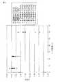
図1に、本発明の一実施形態に係る方法で製造されたCIS系薄膜太陽電池の基本構造を示す。図1において、1は高歪点ガラス基板であり、Na2Oを2〜5重量%含んでいる。2はシリカ(SiOx)を材料とするアルカリ制御層、3はMoを材料とする裏面電極層、4はCIS系半導体で構成されるCIS系光吸収層、5は高抵抗バッファ層、6はn型透明導電膜で形成される窓層を示す。FIG. 1 shows a basic structure of a CIS-based thin film solar cell manufactured by a method according to an embodiment of the present invention. In FIG. 1,
次に、図1の太陽電池セルの各構成要素について、その詳細および変形例を説明する。 Next, details and modifications of each component of the solar battery cell of FIG. 1 will be described.
高歪点ガラス基板1は、例えば表1に示すような物性を有している。
なお、本発明の製造方法に使用可能な高歪点ガラス基板は、表1に示す物性を有するものに限定されるものではない。一般の高歪点ガラスは、Na2Oを1〜7重量%の範囲で含んでおり、このような高歪点ガラスを用いても本発明に係る製造方法を実施することは可能である。また、この条件を外れる高歪点ガラスも存在するが、そのようなガラスであっても本発明に係る製造方法を実施することは可能である。The high strain point glass substrate that can be used in the production method of the present invention is not limited to those having the physical properties shown in Table 1. General high strain point glass contains Na2 O in a range of 1 to 7% by weight, and the manufacturing method according to the present invention can be carried out using such high strain point glass. There are also high strain point glasses that deviate from this condition, but the manufacturing method according to the present invention can be carried out even with such glasses.
次に、アルカリ制御層2の構造および成膜方法について述べる。後述する図2に本発明の実施例として記載するサンプル1〜14については、アルカリ制御層2を膜厚が3〜12nm、屈折率が1.45〜1.50(波長633nmの光に対する屈折率)の範囲となるシリカ膜によって形成した。しかしながら、本発明は特にこの値に限定されること無く、膜厚が15nm以下の範囲のシリカ膜であれば良い。また、シリカ膜以外にも、例えば、SiNx等で適切な膜厚・屈折率としても良い。Next, the structure of the
このようなアルカリ制御層2は、例えば、SiO2またはSiをターゲットとして、1)RFスパッタ法、2)ACスパッタ法、3)DCスパッタ法によって成膜可能である。この場合、投入電力、O2濃度、成膜圧力をパラメータとして変化させることで、種々の膜厚および屈折率を有するシリカ膜を成膜することができる。なお、これ以外のパラメータとして、ガス流量や基板搬送速度等もある。Such an
以下に、アルカリ制御層2の成膜パラメータの一例を示す。
RFスパッタ法:SiO2ターゲット
投入電力:0.1〜3.0W/cm2
O2濃度(O2/O2+Ar):0〜20vol%
成膜圧力:0.3〜2.0PaBelow, an example of the film-forming parameter of the
RF sputtering method: SiO2 target Input power: 0.1 to 3.0 W / cm2
O2 concentration (O2 / O2 + Ar): 0 to 20 vol%
Film forming pressure: 0.3 to 2.0 Pa
なお、アルカリ制御層2の成膜方法としては、上記のスパッタ法以外に、プラズマCVD法、電子ビーム蒸着法などがあり、これらの方法を用いても本発明を実施することは可能である。 In addition to the sputtering method described above, the
アルカリ制御層2の構造を特定するために、膜厚だけではなく屈折率も重要である。基板からCIS系光吸収層へのアルカリ元素(特にNa)の拡散量は、アルカリ制御層2の膜厚に依存するところが大きいが、アルカリ制御層2の屈折率、言い換えれば、密度や組成といった膜質も影響することを、発明者は実験で確認した。よって、本発明の一実施形態に係る製造方法では、アルカリ制御層2を、屈折率が1.45〜1.50(波長633nmの光に対する屈折率)となるように成膜する。 In order to specify the structure of the
即ち、本発明の一実施形態では、高い光電変換効率を有するCIS系薄膜太陽電池を製造するために、屈折率が1.45〜1.50の例えばシリカ膜等を材料とするアルカリ制御層2を、膜厚15nm以下で、高歪点ガラス上に形成することが重要である。 That is, in one embodiment of the present invention, in order to manufacture a CIS-based thin film solar cell having high photoelectric conversion efficiency, the
裏面電極層3は通常、Moを材料としてDCスパッタ法により形成される。表2に、裏面電極層3の膜厚、成膜方法を示す。 The
本発明者等の実験によれば、この分野で通常行われている成膜方法によってMoの裏面電極3を形成する場合、その膜厚が200〜500nmの範囲内であれば、製造されたCIS系薄膜太陽電池の光電変換効率にそれ程大きな影響を与えないことが確認されている。 According to the experiments by the present inventors, when the Mo back
次に、CIS系光吸収層4の詳細を示す。CIS系光吸収層4は、裏面電極層3上に、Cu、In、Gaを含む積層構造又は混晶の金属プリカーサー膜を、スパッタ法や蒸着法などにより成膜した後、これをセレン化および硫化することによって形成する。一実施形態では、InおよびGaのIII族元素の原子数に対するCuの原子数の比率(Cu/III族比)を0.85〜0.95とし、III族元素の原子数に占めるGaの原子数の比率(Ga/III族比)を0.15〜0.4とし、セレン化を350℃〜600℃、硫化を550℃〜650℃の条件で実行することにより、p型の導電型を有する膜厚1〜3μmの光吸収層を成膜した。 Next, the detail of the CIS type
後述する図2に本発明の実施例として記載するサンプル1から20では、CIS系光吸収層4として2セレン・イオウ化銅インジウム・ガリウム(Cu(InGa)(SeS)2)を成膜したが、本発明はこの構成に限定されること無く、I−III−VI2族カルコパイライト半導体であれば良い。In
例えば、
2セレン化銅インジウム (CuInSe2)
2イオウ化銅インジウム (CuInS2)
2セレン・イオウ化銅インジウム (CuIn(SeS)2)
2セレン化銅ガリウム (CuGaSe2)
2イオウ化銅ガリウム (CuGaS2)
2セレン化銅インジウム・ガリウム (Cu(InGa)Se2)
2イオウ化銅インジウム・ガリウム (Cu(InGa)S2)
等であってもよい。For example,
Copper indium selenide (CuInSe2 )
Copper indium disulfide (CuInS2 )
2Selenium and copper indium sulfide (CuIn (SeS)2 )
Copper gallium selenide (CuGaSe2 )
Copper gallium disulfide (CuGaS2 )
Copper indium selenide indium gallium (Cu (InGa) Se2 )
Copper Indium Gallium Sulphide (Cu (InGa) S2 )
Etc.
本発明の一実施形態では、裏面電極層3上に、Cu、In、Gaを含む積層構造又は混晶の金属プリカーサー膜をスパッタ法や蒸着法などにより成膜する時点で、スパッタターゲットあるいは蒸着源に金属プリカーサー膜材料(例えば、CuGa)と共にNaを含ませる。この場合、例えばNaFを含むCuGa合金のスパッタターゲットを使用して、裏面電極層3上にNaを含んだCuGa膜を成膜し、その上に、Inスパッタターゲットを使用して、In膜を成膜する。これにより、Naを含んだ金属プリカーサー膜が形成される。 In one embodiment of the present invention, a sputter target or a deposition source is formed at the time when a multilayered or mixed crystal metal precursor film containing Cu, In, and Ga is formed on the
この後のセレン化および硫化過程において、金属プリカーサー膜に含まれるNaと、高歪点ガラスからのアルカリ元素の拡散とによって、結晶品質が良いCIS系光吸収層が形成される。なお、本実施形態では、スパッタターゲットに含有させるNaをNaFとしたが、Na単体やその他のNa化合物であってもよい。さらに、CuGa合金のスパッタターゲットにNaを含有させる代わりに、InスパッタターゲットやCuスパッタターゲットにNa(NaF等の化合物を含む)を含有させる構成であってもよい。 In the subsequent selenization and sulfidation processes, a CIS-based light absorption layer with good crystal quality is formed by Na contained in the metal precursor film and diffusion of alkali elements from the high strain point glass. In this embodiment, NaF contained in the sputtering target is NaF, but Na alone or other Na compounds may be used. Furthermore, instead of containing Na in the CuGa alloy sputtering target, the In sputtering target or the Cu sputtering target may contain Na (including a compound such as NaF).
次に、バッファ層5の詳細を示す。本発明の一実施形態では、バッファ層5として、n型の導電型を有し透明で高抵抗な、膜厚2〜50nmのZn(O、S、OH)xを成膜することができる。このバッファ層5は、溶液成長法、MOCVD法等によって成膜することが可能である。なお、本実施形態では、バッファ層5としてZn(O、S、OH)xからなる半導体膜を成膜したが、本発明はこの実施形態に限定されることはない。例えば、CdS、ZnS、ZnO等のII−VI族化合物半導体薄膜、これらの混晶であるZn(O、S)x等、例えば、In2O3、In2S3、In(OH)等のIn系化合物半導体薄膜であっても良い。Next, details of the
次に、窓層(透明導電膜)6の詳細を示す。本発明の一実施形態では、n型の導電型を有し、禁制帯幅が広く透明で抵抗値が低く、厚さ0.5〜2.5μmのZnO:Bからなる半導体膜を成膜した。この窓層6は、スパッタ法、MOCVD法によって成膜可能である。また、ZnO:B以外にも、ZnO:Al、ZnO:Gaを使用可能であり、更に、ITO(Indium Tin Oxide)、SnO2等からなる半導体膜であっても良い。Next, details of the window layer (transparent conductive film) 6 will be shown. In one embodiment of the present invention, a semiconductor film made of ZnO: B having an n-type conductivity, a wide forbidden band width, a transparent, low resistance value, and a thickness of 0.5 to 2.5 μm is formed. . This
本発明の一実施形態では、NaをCIS系光吸収層4に添加するために、CIS系光吸収層4の金属プリカーサー膜を形成するスパッタターゲット中にNaを含有させることができる。本発明の他の実施形態では、裏面電極層3を形成するスパッタターゲット中にNaを含有させてもよい。さらに他の実施形態では、1)アルカリ制御層2の形成後であって裏面電極層3を形成する前の時点で、2)裏面電極層3の形成後であって金属プリカーサー膜の形成前の時点で、3)金属プリカーサー膜の形成後に、Na元素を含むミストを基板に塗布することによって、CIS系光吸収層4中に所定量のNaを添加する方法を取ることができる。この場合、Naは、ミスト塗布後のセレン化および硫化処理に伴う熱処理により、CIS系光吸収層4中で熱拡散により均一に分散する。さらに他の実施形態として、CIS系光吸収層4を同時蒸着法によって形成する場合、Na(またはNa化合物)を新たな蒸着源として加える、若しくは、Naを他の蒸着源(CuやGa等)に添加することによって、CIS系光吸収層4中にNaを添加することができる。また、上記1)、2)の時点でNaを添加した後、同時蒸着法によってCIS系光吸収層4を形成することで、同時蒸着に伴う熱処理によってCIS系光吸収層4中にNaが均一に熱拡散する。さらに他の実施形態として、金属プリカーサー膜を積層構造で形成する場合、金属プリカーサー膜を構成する積層された金属膜(例えば、Cu層、Ga層、CuGa層、In層等)の間に、Na化合物(例えば、NaFやNaS等)の層を形成することによって、金属プリカーサー膜中にNaを添加してもよい。 In one embodiment of the present invention, in order to add Na to the CIS
さらに他の実施形態として、CIS系光吸収層4を形成(セレン化・硫化、または、同時蒸着)した後の時点で、Na元素を含むミストをCIS系光吸収層4上に塗布し、これをアニール処理することによって、CIS系光吸収層4中に所定量のNaを添加する方法を取ることができる。 As yet another embodiment, at the time after the CIS-based
本発明者等は、図1に示す構造のCIS系薄膜太陽電池において、CIS系光吸収層4におけるNa濃度をどのように制御すれば、高い光電変換効率を有するCIS系薄膜太陽電池を得ることができるかを明らかにするために、図2に示すような種々の実験を行った。 The present inventors obtain a CIS thin film solar cell having high photoelectric conversion efficiency by controlling how the Na concentration in the CIS
図2は、図1の構造のCIS系薄膜太陽電池において、アルカリ制御層2の膜厚と、金属プリカーサー膜を成膜する場合のスパッタターゲット中に混入するNaの添加量以外の条件を同じにして、複数のCIS系薄膜太陽電池を製造し、それぞれのCIS系薄膜太陽電池の光電変換効率を測定した結果を示す。具体的には、アルカリ制御層2の膜厚として、0nm、3nm、12nm、30nmの4種類のパラメータを選択し、Naを混入するスパッタターゲットとしてCuGaを選択し、Na添加量としては、0原子数%(at%)、0.02原子数%、0.03原子数%、0.05原子数%、0.1原子数%、0.15原子数%の6つのパラメータを選択した。なお、上記のNa添加量を示す「原子数%」は、CIS系光吸収層の原子数に対するものであり、本実施例においては、Cu、Ga、In、Se、Sの原子数を合計したものに対する原子数比である。また、本実施形態においては、裏面電極層3上に金属プリカーサー膜を成膜するにあたり、NaFを添加したCuGaターゲットを用いたCuGa膜と、NaFを添加していないCuGaターゲットを用いたCuGa膜とを積層し、この2つのCuGa膜の膜厚比を調整することで、金属プリカーサー膜中に混入するNaの添加量を調整している。実験に用いたCIS系薄膜太陽電池の高歪点ガラス基板1、アルカリ制御層2、裏面電極層3の構造、成膜条件は、以下の表3に示すとおりである。なお、CIS系光吸収層4、バッファ層5、窓層6の構造および成膜条件は、Naの添加量を除き、前述した範囲内で成膜しており、図2に示す実験に用いたサンプル1〜45において、その構造および成膜条件は同じである。また、本実施形態は、30cm角の太陽電池モジュールとして実験を行った。 FIG. 2 shows the CIS-based thin film solar cell having the structure shown in FIG. 1 with the same conditions except for the thickness of the
まず、図2について説明する。図2に示すサンプル1〜45は、アルカリ制御層2の膜厚と金属プリカーサー膜中のNa添加量が異なるのみで、その他の構造、成膜条件を同じにして作成されたCIS系薄膜太陽電池を示す。図2では、これらの各サンプルについて、アルカリ制御層2の膜厚およびNa添加量(CIS系光吸収層4中のNaの原子数%)と、光電変換効率(Eff)の関係を示している。サンプル1〜20のCIS系薄膜太陽電池は何れも高い光電変換効率を有し、CIS系光吸収層4におけるNa濃度の制御は良好に行われているものと考えられる。従って、サンプル1〜20を本発明の一実施形態に係る方法により製造されたサンプル、即ち、本発明の実施例と称する。 First, FIG. 2 will be described.
サンプル1〜10はアルカリ制御層2の膜厚を3nmとして、金属プリカーサー膜中のNa添加量を0.1原子数%、0.02原子数%、0.03原子数%、および0.05原子数%の4種類の値に変化させている。サンプル11〜20では、アルカリ制御層2の膜厚を12nmとして、金属プリカーサー膜中のNa添加量を0.1原子数%、0.02原子数%、および0.05原子数%の3種類の値に変化させてCIS系薄膜太陽電池を作成した。図2の光電変換効率[Eff]の欄に示すように、サンプル1〜20では、膜厚の変化、Na添加量の変化に関わらず、何れも高い光電変換効率を達成することができた。 In
サンプル21〜29では、アルカリ制御層2の膜厚を3nm、12nm、30nmに変化させる一方、金属プリカーサー膜中にNaを添加することなく(Na添加量0)、CIS系薄膜太陽電池の製造を行った結果を示す。これらのCIS系薄膜太陽電池の光電変換効率は、サンプル1〜20の場合よりも低く、実用に耐えうる値ではない。従ってこれらのサンプルを本発明の実施例から除外し、第1比較例とする。第1比較例のサンプルでは、アルカリ制御層2の層厚を3nmと極めて薄くして、高歪点ガラス基板1からのNaのCIS系光吸収層4への拡散を増加させても、高い光電変換効率を達成することはできなかった。また、膜厚を厚くするに従って、光電変換効率は低下している。このことから、CIS系薄膜太陽電池を製造するにあたって、高歪点ガラス基板1からのNaの拡散のみでは、高い光電変換効率を達成することが可能な量のNaをCIS系光吸収層4に供給できていないことが分かる。 In
サンプル30〜35は、アルカリ制御層2の膜厚を30nmとして高歪点ガラス基板1からCIS系光吸収層4へのNaの拡散をほぼ阻止し、その上で、金属プリカーサー膜中にNaを添加することにより形成したCIS系薄膜太陽電池を示す。サンプル30〜35を第2比較例とする。第2比較例では各サンプルの光電変換効率はサンプル1〜20に比べて一様に低い。例えば、Naの添加量を0.05原子数%としたサンプル30、31の場合、Naの添加量を0として膜厚を3nm、12nmとしたサンプル21〜27の場合よりも光電変換効率が低い。Naの添加量を0.1原子数%とした場合に光電変換効率は改善されるが、しかしその値は、本発明の実施例であるサンプル1〜20の場合よりも低い。 In
サンプル36〜45は、アルカリ制御層2を設けることなく製造したCIS系薄膜太陽電池を示す。サンプル36〜45を第3比較例とする。第3比較例では各サンプルの光電変換効率は、サンプル1〜20に比べてバラツキが生じている。例えば、サンプル36と37や、サンプル40と41を比較すると、同じ構造・成膜条件にもかかわらず、光電変換効率に大きな差が生じている。これは、アルカリ制御層2を設けていないために、高歪点ガラス基板1から、Na以外の不純物がCIS系光吸収層に溶出することに起因し、サンプルによって、この不純物の溶出量が異なるとともに、一つのサンプル内において、局所的に不純物の溶出量が増加したためと考えられる。
図3および図4は、図2に示すデータをグラフ化して示すものである。図3では、Naの添加量をパラメータとした場合の、アルカリ制御層(シリカ層)の膜厚(横軸)に対する光電変換効率Eff(縦軸)の関係をプロットしている。また、図4では、図2に示すデータを、アルカリ制御層2の膜厚をパラメータとして、Naの添加量(横軸)に対する光電変換効率Eff(縦軸)の関係をプロットしている。 3 and 4 are graphs showing the data shown in FIG. In FIG. 3, the relationship of the photoelectric conversion efficiency Eff (vertical axis) with respect to the film thickness (horizontal axis) of the alkali control layer (silica layer) when the addition amount of Na is used as a parameter is plotted. Further, in FIG. 4, the relationship between the photoelectric conversion efficiency Eff (vertical axis) and the amount of Na added (horizontal axis) is plotted with the data shown in FIG. 2 using the film thickness of the
図3を参照すると、高歪点ガラス基板1からの拡散によるNa以外に外部からNaを添加しない第1比較例のサンプル21〜29(図3において×で示す)では、本実施例のサンプル(図において□で示す)によって達成される高い光電変換効率を達成することはない。これは、CIS系光吸収層4へのアルカリ元素(特に、Na)の拡散量が不足しているためであると考えられる。 Referring to FIG. 3,
第1比較例のサンプルに注目すると、サンプル28、29よりサンプル24〜27の光電変換効率は高く、サンプル24〜27よりサンプル21〜23の光電変換効率は高くなっている。これは、アルカリ制御層2の膜厚が薄くなるほど、高歪点ガラス基板1からのアルカリ元素の拡散量が大きくなり、その結果、CIS系光吸収層4の品質が向上したためであると考えられる。 When paying attention to the sample of the first comparative example, the photoelectric conversion efficiency of the samples 24-27 is higher than that of the
また、高歪点ガラス基板1からのアルカリ元素の拡散を阻止した上で、ガラス基板1以外からNaをCIS系光吸収層4に添加した第2比較例のサンプルでは、光電変換効率が13%を超えることはなかった。この第2比較例のサンプルについて、図4を参照すると、サンプル30、31は、サンプル32、33に比べて光電変換効率が低いことから、サンプル30、31の場合、CIS系光吸収層4へのアルカリ元素(特に、Na)の拡散量が不足しているものと考えられる。しかしながら、サンプル34、35のように、Na添加量を増加させても、サンプル32、33より光電変換効率が向上することはなく、サンプル32、33に比べて光電変換効率が低下している。これは、基板以外からNaを添加した場合には、ある一定量まではCIS系光吸収層4の品質向上に寄与するものの、基板以外からの一定量を超える過剰なNaの添加によって、CIS系光吸収層4内でのNaの分布が不均一となり、またCIS系光吸収層4と裏面電極層3との間に微細なハクリが生じた結果、光電変換効率が低下するのではないか、と考えられる。 Further, in the sample of the second comparative example in which Na from other than the
上記の結果から、CIS系光吸収層4へのアルカリ元素の導入量が、光電変換効率の向上に寄与することは明らかであるが、この導入量を調節するだけでは高い光電変換効率を達成することは困難であり、CIS系光吸収層4のアルカリ元素の導入方法が、光電変換効率の改善に大きく影響していることが分かる。より詳細には、第2比較例のように、ガラス基板1以外からのNaの添加だけでは、添加量が充分であったとしても、光電変換効率の大きな改善は望めず、本実施形態のように、基板と基板以外との両面からCIS系光吸収層4にアルカリ元素を導入することにより、高い光電変換効率を達成することが可能となる。これは、CIS系光吸収層4の成膜工程中の熱処理において、ガラス基板1に含まれるアルカリ元素が、この熱処理中、CIS系光吸収層4に常に供給され続け、さらに、高歪点ガラスであるガラス基板1からだけでは不足するアルカリ元素の拡散量を、ガラス基板1以外から添加するという、2つの作用が相乗効果を奏することにより、CIS系光吸収層4の品質が大きく向上するためである。 From the above results, it is clear that the amount of alkali element introduced into the CIS-based
なお、本実施形態においては、アルカリ制御層は必須の構成としている。これは、ガラス基板1からのアルカリ元素の湧き出し方は均一ではないため、アルカリ制御層2を設けることにより、CIS系光吸収層4へのアルカリ元素の拡散を均一にし、CIS系光吸収層4の膜品質の均一性を向上させる効果を奏する。さらに、ガラス基板1にはCIS系光吸収層4にとって不要な元素が含まれており、アルカリ制御層2を設けることによって、ガラス基板1からの不要な元素の拡散が防止されるという、もう1つの作用効果を奏する。 In the present embodiment, the alkali control layer has an essential configuration. This is because the alkali element is not uniformly discharged from the
1 高歪点ガラス基板
2 アルカリ制御層
3 裏面電極層
4 CIS系光吸収層
5 バッファ層
6 透明導電膜(窓層)DESCRIPTION OF
Claims (8)
Translated fromJapanese前記アルカリ制御層上に裏面電極層を形成し、
前記裏面電極層上に少なくともCuとInを含む金属プリカーサー膜を形成し、
前記金属プリカーサー膜を570℃以上の温度でセレン化/硫化してCIS系光吸収層を形成し、
前記CIS系光吸収層上にn型透明導電膜を形成する、各ステップを備え、
前記アルカリ制御層は、屈折率が1.45〜1.50の範囲のシリカ膜を3〜12nmの膜厚に形成したものであり、さらに、前記金属プリカーサー膜には前記高歪点ガラス基板からの熱拡散以外に外部よりアルカリ金属が添加されることを特徴とする、CIS系薄膜太陽電池の製造方法。An alkali control layer is formed on a high strain point glass substrate,
Forming a back electrode layer on the alkali control layer;
Forming a metal precursor film containing at least Cu and In on the back electrode layer;
The metal precursor film is selenized / sulfurized at a temperature of 570 ° C. or higher to form a CIS light absorption layer,
Each step of forming an n-type transparent conductive film on the CIS-based light absorption layer comprises:
The alkali control layer is formed by forming a silica film having a refractive index in the range of 1.45 to 1.50 to a thickness of 3 to 12 nm. Further, the metal precursor film is formed from the high strain point glass substrate. A method for producing a CIS-based thin-film solar cell, wherein an alkali metal is added from the outside in addition to thermal diffusion.
Priority Applications (1)
| Application Number | Priority Date | Filing Date | Title |
|---|---|---|---|
| JP2012036194AJP5575163B2 (en) | 2012-02-22 | 2012-02-22 | CIS type thin film solar cell manufacturing method |
Applications Claiming Priority (1)
| Application Number | Priority Date | Filing Date | Title |
|---|---|---|---|
| JP2012036194AJP5575163B2 (en) | 2012-02-22 | 2012-02-22 | CIS type thin film solar cell manufacturing method |
Related Parent Applications (1)
| Application Number | Title | Priority Date | Filing Date |
|---|---|---|---|
| JP2009285318ADivisionJP2011129631A (en) | 2009-12-16 | 2009-12-16 | Method of manufacturing cis thin film solar cell |
Publications (2)
| Publication Number | Publication Date |
|---|---|
| JP2012124524Atrue JP2012124524A (en) | 2012-06-28 |
| JP5575163B2 JP5575163B2 (en) | 2014-08-20 |
Family
ID=46505579
Family Applications (1)
| Application Number | Title | Priority Date | Filing Date |
|---|---|---|---|
| JP2012036194AActiveJP5575163B2 (en) | 2012-02-22 | 2012-02-22 | CIS type thin film solar cell manufacturing method |
Country Status (1)
| Country | Link |
|---|---|
| JP (1) | JP5575163B2 (en) |
Citations (6)
| Publication number | Priority date | Publication date | Assignee | Title |
|---|---|---|---|---|
| JPH11135819A (en)* | 1997-10-31 | 1999-05-21 | Matsushita Electric Ind Co Ltd | Compound thin film solar cell |
| JPH11274534A (en)* | 1998-03-25 | 1999-10-08 | Yazaki Corp | I-III-VI group compound semiconductor and thin film solar cell using the same |
| JP2003318424A (en)* | 2002-04-18 | 2003-11-07 | Honda Motor Co Ltd | Thin film solar cell and method of manufacturing the same |
| JP2006165386A (en)* | 2004-12-09 | 2006-06-22 | Showa Shell Sekiyu Kk | CIS thin film solar cell and method for producing the same |
| JP2007201302A (en)* | 2006-01-30 | 2007-08-09 | Honda Motor Co Ltd | Solar cell and method for manufacturing the same |
| JP2009283560A (en)* | 2008-05-20 | 2009-12-03 | Showa Shell Sekiyu Kk | Production process of cis-based thin film solar cell |
- 2012
- 2012-02-22JPJP2012036194Apatent/JP5575163B2/enactiveActive
Patent Citations (6)
| Publication number | Priority date | Publication date | Assignee | Title |
|---|---|---|---|---|
| JPH11135819A (en)* | 1997-10-31 | 1999-05-21 | Matsushita Electric Ind Co Ltd | Compound thin film solar cell |
| JPH11274534A (en)* | 1998-03-25 | 1999-10-08 | Yazaki Corp | I-III-VI group compound semiconductor and thin film solar cell using the same |
| JP2003318424A (en)* | 2002-04-18 | 2003-11-07 | Honda Motor Co Ltd | Thin film solar cell and method of manufacturing the same |
| JP2006165386A (en)* | 2004-12-09 | 2006-06-22 | Showa Shell Sekiyu Kk | CIS thin film solar cell and method for producing the same |
| JP2007201302A (en)* | 2006-01-30 | 2007-08-09 | Honda Motor Co Ltd | Solar cell and method for manufacturing the same |
| JP2009283560A (en)* | 2008-05-20 | 2009-12-03 | Showa Shell Sekiyu Kk | Production process of cis-based thin film solar cell |
Also Published As
| Publication number | Publication date |
|---|---|
| JP5575163B2 (en) | 2014-08-20 |
Similar Documents
| Publication | Publication Date | Title |
|---|---|---|
| JP4540724B2 (en) | CIS type thin film solar cell manufacturing method | |
| JP4384237B2 (en) | CIS type thin film solar cell manufacturing method | |
| Jo et al. | 8% Efficiency Cu2ZnSn (S, Se) 4 (CZTSSe) thin film solar cells on flexible and lightweight molybdenum foil substrates | |
| CN102934235B (en) | Thin film solar cell | |
| US8501519B2 (en) | Method of production of CIS-based thin film solar cell | |
| US20110018089A1 (en) | Stack structure and integrated structure of cis based solar cell | |
| JP5709662B2 (en) | CZTS thin film solar cell manufacturing method | |
| KR101628312B1 (en) | PREPARATION METHOD OF CZTSSe-BASED THIN FILM SOLAR CELL AND CZTSSe-BASED THIN FILM SOLAR CELL PREPARED BY THE METHOD | |
| US20150059845A1 (en) | Czts-based thin film solar cell and method of production of same | |
| CN106653946B (en) | A kind of deposition method of cadmium telluride thin film solar cell absorption layer | |
| JP6297038B2 (en) | Thin film solar cell and method for manufacturing thin film solar cell | |
| EP2702615B1 (en) | Method of preparing a solar cell | |
| US8962379B2 (en) | Method of producing CIGS film, and method of producing CIGS solar cell by using same | |
| US20120118384A1 (en) | Cis-based thin film solar cell | |
| CN113228304B (en) | Photoelectric conversion element and method for manufacturing the same | |
| KR102057234B1 (en) | Preparation of CIGS thin film solar cell and CIGS thin film solar cell using the same | |
| JP5575163B2 (en) | CIS type thin film solar cell manufacturing method | |
| EP2999004A1 (en) | Photoelectric conversion device, and solar cell | |
| JP6961325B2 (en) | Manufacturing method of photoelectric conversion layer and manufacturing method of photoelectric conversion element | |
| US20210210645A1 (en) | Chalcogenide solar cell having transparent conducting oxide back contact, and method of manufacturing the chalcogenide solar cell | |
| JP2012004427A (en) | Cis-based thin-film solar cell | |
| WO2017043596A1 (en) | Photoelectric conversion element | |
| KR20150136706A (en) | Solar cell | |
| CN102446989A (en) | Photovoltaic device and method for making |
Legal Events
| Date | Code | Title | Description |
|---|---|---|---|
| A977 | Report on retrieval | Free format text:JAPANESE INTERMEDIATE CODE: A971007 Effective date:20130523 | |
| A131 | Notification of reasons for refusal | Free format text:JAPANESE INTERMEDIATE CODE: A131 Effective date:20130528 | |
| A521 | Request for written amendment filed | Free format text:JAPANESE INTERMEDIATE CODE: A523 Effective date:20130723 | |
| A131 | Notification of reasons for refusal | Free format text:JAPANESE INTERMEDIATE CODE: A131 Effective date:20140225 | |
| A521 | Request for written amendment filed | Free format text:JAPANESE INTERMEDIATE CODE: A523 Effective date:20140422 | |
| TRDD | Decision of grant or rejection written | ||
| A01 | Written decision to grant a patent or to grant a registration (utility model) | Free format text:JAPANESE INTERMEDIATE CODE: A01 Effective date:20140603 | |
| A61 | First payment of annual fees (during grant procedure) | Free format text:JAPANESE INTERMEDIATE CODE: A61 Effective date:20140701 | |
| R150 | Certificate of patent or registration of utility model | Ref document number:5575163 Country of ref document:JP Free format text:JAPANESE INTERMEDIATE CODE: R150 | |
| S111 | Request for change of ownership or part of ownership | Free format text:JAPANESE INTERMEDIATE CODE: R313111 | |
| R350 | Written notification of registration of transfer | Free format text:JAPANESE INTERMEDIATE CODE: R350 | |
| R250 | Receipt of annual fees | Free format text:JAPANESE INTERMEDIATE CODE: R250 | |
| R250 | Receipt of annual fees | Free format text:JAPANESE INTERMEDIATE CODE: R250 | |
| R250 | Receipt of annual fees | Free format text:JAPANESE INTERMEDIATE CODE: R250 | |
| R250 | Receipt of annual fees | Free format text:JAPANESE INTERMEDIATE CODE: R250 | |
| R250 | Receipt of annual fees | Free format text:JAPANESE INTERMEDIATE CODE: R250 |