JP2012109809A - Antenna device - Google Patents
Antenna deviceDownload PDFInfo
- Publication number
- JP2012109809A JP2012109809AJP2010257195AJP2010257195AJP2012109809AJP 2012109809 AJP2012109809 AJP 2012109809AJP 2010257195 AJP2010257195 AJP 2010257195AJP 2010257195 AJP2010257195 AJP 2010257195AJP 2012109809 AJP2012109809 AJP 2012109809A
- Authority
- JP
- Japan
- Prior art keywords
- antenna device
- capacitive coupling
- ground terminal
- coupling element
- opposite side
- Prior art date
- Legal status (The legal status is an assumption and is not a legal conclusion. Google has not performed a legal analysis and makes no representation as to the accuracy of the status listed.)
- Withdrawn
Links
Images


Landscapes
- Details Of Aerials (AREA)
Abstract
Translated fromJapaneseDescription
Translated fromJapanese本発明は、携帯電話等の携帯無線端末に用いられるアンテナ装置に関し、1.5GHz帯を含む複数の周波数帯での使用に好適なアンテナ装置に関する。 The present invention relates to an antenna device used for a portable wireless terminal such as a mobile phone, and more particularly to an antenna device suitable for use in a plurality of frequency bands including a 1.5 GHz band.
携帯電話等の携帯無線機端末においては、各種アプリケーションの増大による高機能化が要求されている。また、将来的にサービスされるLTE(Long Term Evolution、携帯電話の通信規格)システムの高性能化を図るために周波数帯の増加が見込まれ、それに伴い無線端末用アンテナの更なる多周波帯化が求められる。特に1.5GHz帯においては、日本国内におけるLTE運用の有力な周波数として検討されており、1.5GHz帯を含む複数の周波数帯に対応したアンテナの開発が急務となっている。 In portable radio terminals such as mobile phones, higher functionality is required by increasing various applications. In addition, frequency bands are expected to increase in order to improve the performance of LTE (Long Term Evolution, mobile phone communication standards) systems that will be serviced in the future. Is required. In particular, in the 1.5 GHz band, it has been studied as an influential frequency for LTE operation in Japan, and there is an urgent need to develop an antenna that supports a plurality of frequency bands including the 1.5 GHz band.
今までに提案されている複数の周波数帯に対応したアンテナとして、例えば特許文献1や特許文献2に記載されたものがある。特許文献1には、ラジエータを、接地プレートからある距離離すとともに、接地プレートに略平行に配置し、その端ゾーンの一方で、接地プレートに導電接続するようにし、第1(より低い)共振周波数において、ラジエータと接地プレートの接続点で最小電圧が生じ、ラジエータの自由端の領域で第1最大電圧が生じ、他より高い共振周波数で、最小電圧と第2最大電圧が、それぞれラジエータの前述した端で生じ、ラジエータの自由端の領域がラジエータの他端に容量結合され、ラジエータは2つの周波数範囲での使用が可能となるアンテナ構成が記載されている。また、特許文献2には、折り返し形状のアンテナに上下平板素子を追加して広帯域化を図ったアンテナ装置が記載されている。 As antennas corresponding to a plurality of frequency bands proposed so far, there are antennas described in Patent Document 1 and Patent Document 2, for example. In Patent Document 1, the radiator is separated from the ground plate by a certain distance, and is disposed substantially parallel to the ground plate, and is electrically conductively connected to the ground plate in one of its end zones, and the first (lower) resonance frequency. , The minimum voltage is generated at the connection point between the radiator and the ground plate, the first maximum voltage is generated in the region of the free end of the radiator, and the minimum voltage and the second maximum voltage at the higher resonance frequency than the others, respectively. An antenna configuration is described in which the region of the free end of the radiator that occurs at the end is capacitively coupled to the other end of the radiator and the radiator can be used in two frequency ranges. Further, Patent Document 2 describes an antenna device in which a wide band is achieved by adding upper and lower flat plate elements to a folded antenna.
しかしながら、特許文献1に記載されたアンテナ構成は、アンテナ方式がモノポールアンテナであるため、広帯域化の効果が乏しいという課題がある。また、特許文献2に記載されたアンテナ装置は、広帯域な周波数特性を確保できるアンテナ構成ではあるものの、マルチバンド化した場合における広帯域化が困難であるという課題がある。 However, since the antenna configuration described in Patent Document 1 is a monopole antenna, there is a problem that the effect of widening the band is poor. Moreover, although the antenna device described in Patent Document 2 has an antenna configuration that can ensure a wide band frequency characteristic, there is a problem that it is difficult to widen the band when multiband.
本発明は、係る事情に鑑みてなされたものであり、容易に広帯域化が図れるアンテナ装置を提供することを目的とする。 The present invention has been made in view of such circumstances, and an object of the present invention is to provide an antenna device that can easily achieve a wide band.
本発明のアンテナ装置は、両端が短絡された所定間隔の平行線路を有する折り返しダイポールアンテナの、2つの素子先端部を垂直方向と水平方向に折り曲げたアンテナ装置であって、前記アンテナ装置を構成する素子のうち、隣接する3素子から構成されるコの字形状の平行となる両端2素子の少なくとも1つを導体面とすることにより設けられたスロットと、前記アンテナ装置を構成する素子のうち、隣接する3素子から構成されるコの字形状の中央素子の少なくとも1つに設けられた導体面と、高周波電源に接続された給電端子と、グランドに接続された接地端子と、前記給電端子もしくは前記接地端子の対向側に位置する素子と前記給電端子もしくは前記接地端子との間に設けられたリアクタンス素子と、を備えた。 The antenna device of the present invention is an antenna device in which two element tips are bent in a vertical direction and a horizontal direction of a folded dipole antenna having parallel lines with predetermined intervals shorted at both ends, and constitutes the antenna device. Of the elements constituting the antenna device, a slot provided by using at least one of the two U-shaped parallel two-sided elements composed of three adjacent elements as a conductor surface among the elements, A conductor surface provided in at least one of the U-shaped central elements composed of three adjacent elements, a power supply terminal connected to a high-frequency power supply, a ground terminal connected to the ground, and the power supply terminal or And a reactance element provided between the element located on the opposite side of the ground terminal and the power supply terminal or the ground terminal.
上記構成によれば、高周波電源に接続された給電端子もしくはグランドに接続された接地端子の対向側に位置する素子と給電端子もしくは接地端子との間に設けたリアクタンス素子によって新たな共振経路が形成されるので、同様のアンテナ構成でリアクタンス素子を有しないアンテナ装置と比べて、容易により広帯域化が図れる。しかも、リアクタンス素子を金属片で実現できるので、安価に広帯域化を実現できる。 According to the above configuration, a new resonance path is formed by the reactance element provided between the power supply terminal connected to the high frequency power supply or the element located on the opposite side of the ground terminal connected to the ground and the power supply terminal or ground terminal. Therefore, compared with an antenna device having a similar antenna configuration and no reactance element, a wider band can be easily achieved. In addition, since the reactance element can be realized with a metal piece, a wide band can be realized at a low cost.
上記構成において、前記給電端子から前記接地端子への導体長が第1周波数の2分の1波長の長さを有し、前記給電端子もしくは前記接地端子から前記導体面の周囲を経由したコの字形状の中央素子の先端までの導体長が第2周波数の4分の1波長の長さを有し、前記給電端子もしくは前記接地端子から前記導体面の最短距離を経由したコの字形状の中央素子の先端までの導体長が第3周波数の4分の1波長の長さを有し、前記給電端子もしくは前記接地端子から前記リアクタンス素子を経由したコの字形状の中央素子の先端までの導体長が第4周波数の4分の1波長の長さを有する。 In the above configuration, the conductor length from the power supply terminal to the ground terminal has a length of one-half wavelength of the first frequency, and the conductor length from the power supply terminal or the ground terminal passes through the periphery of the conductor surface. A conductor length up to the tip of the U-shaped central element has a length of a quarter wavelength of the second frequency, and a U-shape having a shortest distance from the power supply terminal or the ground terminal to the conductor surface. The conductor length to the tip of the central element has a length of a quarter wavelength of the third frequency, and extends from the feeding terminal or the ground terminal to the tip of the U-shaped central element via the reactance element. The conductor length has a length of a quarter wavelength of the fourth frequency.
上記構成によれば、第1周波数から第3周波数のそれぞれにおいて共振するとともに、リアクタンス素子を設けたことで第4周波数においても共振するので、同様のアンテナ構成でリアクタンス素子を有しないアンテナ装置と比べて、より広帯域化が図れる。 According to the above configuration, since resonance occurs at each of the first to third frequencies and also at the fourth frequency by providing the reactance element, compared with an antenna device having a similar antenna configuration and no reactance element. Thus, a wider band can be achieved.
上記構成において、前記リアクタンス素子として、前記対向側に位置する素子より容量結合素子を設け、前記容量結合素子は前記接地端子に平行に面し、前記容量結合素子と前記接地端子とが容量的に結合する。 In the above configuration, as the reactance element, a capacitive coupling element is provided from an element located on the opposite side, the capacitive coupling element faces parallel to the ground terminal, and the capacitive coupling element and the ground terminal are capacitively connected. Join.
上記構成によれば、リアクタンス素子としての容量結合素子を接地端子の対向側に位置する素子に設け、接地端子と容量的に結合させるようにしたので、第4周波数においても共振する共振経路を形成でき、同様のアンテナ構成でリアクタンス素子を有しないアンテナ装置と比べて、より広帯域化が図れる。 According to the above configuration, since the capacitive coupling element as the reactance element is provided on the element located on the opposite side of the ground terminal and capacitively coupled to the ground terminal, a resonance path that resonates even at the fourth frequency is formed. In addition, a wider band can be achieved as compared with an antenna device having a similar antenna configuration and no reactance element.
上記構成において、前記リアクタンス素子として、前記対向側に位置する素子より容量結合素子を設け、前記容量結合素子は前記給電端子に平行に面し、前記容量結合素子と前記給電端子とが容量的に結合する。 In the above configuration, as the reactance element, a capacitive coupling element is provided from an element located on the opposite side, the capacitive coupling element faces in parallel to the feeding terminal, and the capacitive coupling element and the feeding terminal are capacitively connected. Join.
上記構成によれば、リアクタンス素子としての容量結合素子を給電端子の対向側に位置する素子に設け、給電端子と容量的に結合させるようにしたので、第4周波数においても共振する共振経路を形成でき、同様のアンテナ構成でリアクタンス素子を有しないアンテナ装置と比べて、より広帯域化が図れる。 According to the above configuration, since the capacitive coupling element as the reactance element is provided on the element located on the opposite side of the power supply terminal and is capacitively coupled to the power supply terminal, a resonance path that resonates even at the fourth frequency is formed. In addition, a wider band can be achieved as compared with an antenna device having a similar antenna configuration and no reactance element.
上記構成において、前記リアクタンス素子として、前記接地端子より容量結合素子を設け、前記容量結合素子は前記対向側に位置する素子に平行に面し、前記容量結合素子と前記対向側に位置する素子とが容量的に結合する。 In the above configuration, as the reactance element, a capacitive coupling element is provided from the ground terminal, the capacitive coupling element faces in parallel to the element located on the opposite side, and the capacitive coupling element and the element located on the opposite side; Are capacitively coupled.
上記構成によれば、リアクタンス素子としての容量結合素子を接地端子に設け、接地端子の対向側に位置する素子と容量的に結合させるようにしたので、第4周波数においても共振する共振経路を形成でき、同様のアンテナ構成でリアクタンス素子を有しないアンテナ装置と比べて、より広帯域化が図れる。 According to the above configuration, since the capacitive coupling element as the reactance element is provided on the ground terminal and capacitively coupled to the element located on the opposite side of the ground terminal, a resonance path that resonates even at the fourth frequency is formed. In addition, a wider band can be achieved as compared with an antenna device having a similar antenna configuration and no reactance element.
上記構成において、前記リアクタンス素子として、前記給電端子より容量結合素子を設け、前記容量結合素子は前記対向側に位置する素子に平行に面し、前記容量結合素子と前記対向側に位置する素子とが容量的に結合する。 In the above configuration, as the reactance element, a capacitive coupling element is provided from the power supply terminal, the capacitive coupling element faces in parallel to the element located on the opposite side, and the capacitive coupling element and the element located on the opposite side; Are capacitively coupled.
上記構成によれば、リアクタンス素子としての容量結合素子を給電端子に設け、給電端子の対向側に位置する素子と容量的に結合させるようにしたので、第4周波数においても共振する共振経路を形成でき、同様のアンテナ構成でリアクタンス素子を有しないアンテナ装置と比べて、より広帯域化が図れる。 According to the above configuration, since the capacitive coupling element as the reactance element is provided in the power supply terminal and capacitively coupled to the element located on the opposite side of the power supply terminal, a resonance path that resonates even at the fourth frequency is formed. In addition, a wider band can be achieved as compared with an antenna device having a similar antenna configuration and no reactance element.
上記構成において、前記対向側に位置する素子と前記容量結合素子との間にリアクタンス成分を有するチップ部品を設けた。 In the above configuration, a chip component having a reactance component is provided between the element located on the opposite side and the capacitive coupling element.
上記構成によれば、給電端子もしくは接地端子の対向側に位置する素子と容量結合素子との間にリアクタンス成分を有するチップ部品を設けたので、共振周波数の調整が可能となる。 According to the above configuration, since the chip component having a reactance component is provided between the element located on the opposite side of the power supply terminal or the ground terminal and the capacitive coupling element, the resonance frequency can be adjusted.
上記構成において、前記対向側に位置する素子と前記容量結合素子との間において、前記容量結合素子に所定の周波数以外の任意の周波数を遮断する遮断回路を設けた。 In the above configuration, a blocking circuit that blocks any frequency other than a predetermined frequency is provided in the capacitive coupling element between the element located on the opposite side and the capacitive coupling element.
上記構成によれば、給電端子もしくは接地端子の対向側に位置する素子と容量結合素子との間において、容量結合素子に所定の周波数以外の任意の周波数を遮断する遮断回路を設けたので、任意の周波数の所定の周波数への干渉を抑制することができる。 According to the above configuration, since the capacitive coupling element is provided with the cutoff circuit that cuts off any frequency other than the predetermined frequency between the element located on the opposite side of the power supply terminal or the ground terminal and the capacitive coupling element, any Interference with a predetermined frequency can be suppressed.
本発明によれば、高周波電源に接続された給電端子もしくはグランドに接続された接地端子の対向側に位置する素子と給電端子もしくは接地端子との間にリアクタンス素子を設けたので、新たな共振経路を形成でき、同様のアンテナ構成でリアクタンス素子を有しないアンテナ装置と比べて、容易により広帯域化が図れる。しかも、リアクタンス素子は金属片で実現できるので、コストアップを最小限に抑えることができる。 According to the present invention, since the reactance element is provided between the power supply terminal connected to the high frequency power source or the element located on the opposite side of the ground terminal connected to the ground and the power supply terminal or the ground terminal, a new resonance path is provided. Compared with an antenna device having a similar antenna configuration and no reactance element, a wider band can be easily achieved. In addition, since the reactance element can be realized with a metal piece, an increase in cost can be minimized.
以下、本発明を実施するための好適な実施の形態について、図面を参照して詳細に説明する。 DESCRIPTION OF EXEMPLARY EMBODIMENTS Hereinafter, preferred embodiments for carrying out the invention will be described in detail with reference to the drawings.
(実施の形態1)
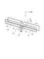
図1は、本発明の実施の形態1に係るアンテナ装置の概略構成を示す斜視図である。同図において、本実施の形態のアンテナ装置1は、両端が短絡された所定間隔の平行線路を有する折り返しダイポールアンテナの2つの素子10a,10bそれぞれの素子先端部100を垂直方向と水平方向に折り曲げたものである。そして、このアンテナ装置1は、これを構成する素子10aのうち、隣接する3素子101,102,103から構成されるコの字形状の平行となる両端2素子101,103の1つを導体面104とすることにより設けられたスロット105と、同じく素子10bのうち、隣接する3素子101,102,103から構成されるコの字形状の平行となる両端2素子101,103の1つを導体面104とすることにより設けられたスロット105と、前述した2つの導体面104と、高周波電源40に接続された平板状の給電端子20と、グランド50に接続された平板状の接地端子30と、接地端子30の対向側に位置する素子106と接地端子30との間に設けられたリアクタンス素子60とを備えている。(Embodiment 1)
FIG. 1 is a perspective view showing a schematic configuration of an antenna apparatus according to Embodiment 1 of the present invention. In the figure, the antenna device 1 according to the present embodiment bends the
このアンテナ装置1は、給電端子20から接地端子30への導体長が第1周波数f1の2分の1波長の長さを有する。また、給電端子20もしくは接地端子30から導体面104の周囲を経由したコの字形状の中央素子102の先端までの導体長が第2周波数f2の4分の1波長の長さを有する。また、給電端子20もしくは接地端子30から導体面104の最短距離を経由したコの字形状の中央素子102の先端までの導体長が第3周波数f3の4分の1波長の長さを有する。また、給電端子20もしくは接地端子30からリアクタンス素子60を経由したコの字形状の中央素子102の先端までの導体長が第4周波数f4の4分の1波長の長さを有する。 In the antenna device 1, the conductor length from the
リアクタンス素子60は、略Lの字形状に形成した金属片を用いた容量結合素子であり、その一端が接地端子30の対向側に位置する素子106に接続され、他端側が接地端子30に平行に面するように対向配置されていて、接地端子30と接地端子30の対向側に位置する素子106とを容量結合している。このようにしてリアクタンス素子60を設けることで、「接地端子30」→「リアクタンス素子60」→「素子106」の新たな電流経路が発生し、アンテナの電気長が長くなる。すなわち、広帯域化が図れる。また、電気長が長くなるもののアンテナの物理的な形状には変化がないことから、実質的にアンテナの小型化が図れる。 The reactance element 60 is a capacitive coupling element using a metal piece formed in a substantially L shape. One end of the reactance element 60 is connected to the
このように、本実施の形態のアンテナ装置1は上述した各導体長を採るので、f1〜f4の4つの共振モードが得られる。しかも、f4の共振モードはリアクタンス素子60を設けたことで得られるものであり、このようなリアクタンス素子60を有しないアンテナ装置よりも、より広帯域化を図ることができる。 Thus, since the antenna device 1 of the present embodiment adopts the above-described conductor lengths, four resonance modes f1 to f4 are obtained. In addition, the resonance mode of f4 is obtained by providing the reactance element 60, and a wider band can be achieved than an antenna device that does not have such a reactance element 60.
ここで、図2は、本実施の形態のアンテナ装置1による広帯域化のVSWR(Voltage Standing Wave Ratio)特性を示す図であり、f1〜f4のそれぞれの周波数においてVSWR値が最低になっている。 Here, FIG. 2 is a diagram showing a broadband VSWR (Voltage Standing Wave Ratio) characteristic by the antenna device 1 of the present embodiment, and the VSWR value is the lowest at each frequency of f1 to f4.
また、図3は、上記4つの共振モードを示す図であり、(a)はf1共振モード、(b)はf2共振モード、(c)はf3共振モード、(d)はf4共振モードである。これらの図において破線矢印は高周波電流の流れる経路を示している。 FIG. 3 is a diagram showing the above four resonance modes, where (a) is the f1 resonance mode, (b) is the f2 resonance mode, (c) is the f3 resonance mode, and (d) is the f4 resonance mode. . In these drawings, broken-line arrows indicate paths through which high-frequency current flows.
このように本実施の形態のアンテナ装置1によれば、グランド50に接続された接地端子30の対向側に位置する素子106と接地端子30との間にリアクタンス素子60を設けたので、新たな共振経路を形成することができ、同様のアンテナ構成でリアクタンス素子60を有しないアンテナ装置と比べて、容易により広帯域化が図れる。しかも、リアクタンス素子60は金属片で実現できるので、コストアップを最小限に抑えることができる。 As described above, according to the antenna device 1 of the present embodiment, since the reactance element 60 is provided between the
なお、本実施の形態では、導体面104を素子101から中央素子102に亘って連続して設けたが、素子101と中央素子102のそれぞれに設けるようにしてもよい。すなわち、一体的に設けるのではなく、部分的に設けるようにしても構わない。 In this embodiment, the
また、本実施の形態では、導体面104を素子101側に設けたが、素子103側に設けてもよいし、素子101と素子103の双方に設けてもよい。但し、素子101と素子103の双方に設ける場合、互いの導体面104が接触しなように、スロット105を必ず確保する。 In this embodiment mode, the
(実施の形態2)
図4は、本発明の実施の形態2に係るアンテナ装置の概略構成を示す斜視図である。同図において、本実施の形態のアンテナ装置2は、リアクタンス素子60を、給電端子20の対向側に位置する素子106と給電端子20との間に設けたものであり、その他の構成は前述した実施の形態1のアンテナ装置1と同様である。上述したようにリアクタンス素子60は、略Lの字形状に形成した金属片を用いた容量結合素子である。このリアクタンス素子60の一端が給電端子20の対向側に位置する素子106に接続され、他端側が給電端子20に平行に面するように対向配置されて、給電端子20と給電端子20の対向側に位置する素子106とを容量結合させる。この実施の形態のアンテナ装置2においても実施の形態1のアンテナ装置1と同様に広帯域化が図れる。(Embodiment 2)
FIG. 4 is a perspective view showing a schematic configuration of the antenna apparatus according to Embodiment 2 of the present invention. In the figure, the antenna device 2 according to the present embodiment is such that the reactance element 60 is provided between the
(実施の形態3)
図5は、本発明の実施の形態3に係るアンテナ装置の概略構成を示す斜視図である。同図において、本実施の形態のアンテナ装置3は、平板状のリアクタンス素子61を接地端子30側に設けたものであり、その他の構成は前述した実施の形態1のアンテナ装置1と同様である。リアクタンス素子61は、その一端側が接地端子30に接続され、他端側が接地端子30の対向側に位置する素子106に平行に面するように対向配置されて、接地端子30と接地端子30の対向側に位置する素子106とを容量結合させる。この実施の形態のアンテナ装置3においても実施の形態1のアンテナ装置1と同様に広帯域化が図れる。(Embodiment 3)
FIG. 5 is a perspective view showing a schematic configuration of the antenna apparatus according to Embodiment 3 of the present invention. In the figure, the antenna device 3 of the present embodiment is provided with a
(実施の形態4)
図6は、本発明の実施の形態4に係るアンテナ装置の概略構成を示す斜視図である。同図において、本実施の形態のアンテナ装置4は、平板状のリアクタンス素子61を給電端子20側に設けたものであり、その他の構成は前述した実施の形態2のアンテナ装置2と同様である。リアクタンス素子61は、その一端側が給電端子20に接続され、他端側が給電端子20の対向側に位置する素子106に平行に面するように対向配置されて、給電端子20と給電端子20の対向側に位置する素子106とを容量結合させる。この実施の形態のアンテナ装置4においても実施の形態1のアンテナ装置1と同様に広帯域化が図れる。(Embodiment 4)
FIG. 6 is a perspective view showing a schematic configuration of an antenna apparatus according to Embodiment 4 of the present invention. In the figure, the antenna device 4 of the present embodiment has a plate-
(実施の形態5)
図7は、本発明の実施の形態5に係るアンテナ装置の概略構成を示す斜視図である。同図において、本実施の形態のアンテナ装置5は、平板状のリアクタンス素子61を前述した実施の形態1のアンテナ装置1と同様に接地端子30側に設けたものであるが、リアクタンス素子61の他に、接地端子30の対向側に位置する素子106とリアクタンス素子61との間にリアクタンス成分を有するチップ部品70を更に設けたものである。このリアクタンス成分を有するチップ部品70を設けることで、共振周波数の調整が可能となる。(Embodiment 5)
FIG. 7 is a perspective view showing a schematic configuration of an antenna apparatus according to Embodiment 5 of the present invention. In the figure, the antenna device 5 of the present embodiment has a
(実施の形態6)
図8は、本発明の実施の形態6に係るアンテナ装置の概略構成を示す斜視図である。同図において、本実施の形態のアンテナ装置6は、前述した実施の形態5のアンテナ装置5と同様に接地端子30側にリアクタンス素子61を設けたものであるが、リアクタンス素子61の他に、接地端子30の対向側に位置する素子106とリアクタンス素子61との間に、f4の周波数以外のf1〜f3の周波数を遮断するフィルタ回路等から構成される遮断回路80を更に設けたものである。この遮断回路80を設けることで、f1〜f3の周波数のf4の周波数への干渉を抑制することができる。(Embodiment 6)
FIG. 8 is a perspective view showing a schematic configuration of an antenna apparatus according to Embodiment 6 of the present invention. In the figure, the antenna device 6 of the present embodiment is provided with a
(実施の形態7)
図9は、本発明の実施の形態7に係るアンテナ装置の概略構成を示す斜視図である。同図において、本実施の形態のアンテナ装置7は、前述した実施の形態5のアンテナ装置5が有するチップ部品70と実施の形態6のアンテナ装置6が有する遮断回路80の双方を有し、これらが接地端子30の対向側に位置する素子106とリアクタンス素子61との間に設けられたものである。チップ部品70を有することで共振周波数の調整が可能であり、また遮断回路80を有することでf1〜f3の周波数のf4の周波数への干渉を抑制することができる。(Embodiment 7)
FIG. 9 is a perspective view showing a schematic configuration of an antenna apparatus according to Embodiment 7 of the present invention. In the figure, the antenna device 7 of the present embodiment includes both the
本発明は、容易に広帯域化かつ小型化が図れるといった効果を有し、将来的にサービスされるLTEシステムの携帯電話等への適用が可能である。 The present invention has an effect that the bandwidth can be easily reduced and the size can be reduced, and can be applied to a cellular phone or the like of an LTE system to be serviced in the future.
1〜7 アンテナ装置
10a,10b,101,102,103 素子
20 給電端子
30 接地端子
40 高周波電源
50 グランド
60,61 リアクタンス素子
70 チップ部品
80 遮断回路
100 素子先端部
104 導体面
105 スロット1 to 7
Claims (8)
Translated fromJapanese前記アンテナ装置を構成する素子のうち、隣接する3素子から構成されるコの字形状の平行となる両端2素子の少なくとも1つを導体面とすることにより設けられたスロットと、
前記アンテナ装置を構成する素子のうち、隣接する3素子から構成されるコの字形状の中央素子の少なくとも1つに設けられた導体面と、
高周波電源に接続された給電端子と、
グランドに接続された接地端子と、
前記給電端子もしくは前記接地端子の対向側に位置する素子と前記給電端子もしくは前記接地端子との間に設けられたリアクタンス素子と、
を備えたアンテナ装置。An antenna device in which two element tips are folded in a vertical direction and a horizontal direction in a folded dipole antenna having parallel lines with predetermined intervals short-circuited at both ends,
Of the elements constituting the antenna device, a slot provided by using at least one of two elements at both ends that are parallel to each other in a U-shape composed of three adjacent elements as a conductor surface;
A conductor surface provided on at least one of U-shaped central elements composed of three adjacent elements among the elements constituting the antenna device;
A power supply terminal connected to a high-frequency power source;
A ground terminal connected to ground, and
A reactance element provided between the power supply terminal or the ground terminal and the element located on the opposite side of the power supply terminal or the ground terminal;
An antenna device comprising:
前記給電端子もしくは前記接地端子から前記導体面の周囲を経由したコの字形状の中央素子の先端までの導体長が第2周波数の4分の1波長の長さを有し、
前記給電端子もしくは前記接地端子から前記導体面の最短距離を経由したコの字形状の中央素子の先端までの導体長が第3周波数の4分の1波長の長さを有し、
前記給電端子もしくは前記接地端子から前記リアクタンス素子を経由したコの字形状の中央素子の先端までの導体長が第4周波数の4分の1波長の長さを有する請求項1に記載のアンテナ装置。A conductor length from the power supply terminal to the ground terminal has a length of a half wavelength of the first frequency;
The conductor length from the feeding terminal or the ground terminal to the tip of the U-shaped central element passing through the periphery of the conductor surface has a length of a quarter wavelength of the second frequency,
The conductor length from the feeding terminal or the ground terminal to the tip of the U-shaped central element via the shortest distance of the conductor surface has a length of a quarter wavelength of the third frequency,
2. The antenna device according to claim 1, wherein a conductor length from the power supply terminal or the ground terminal to a tip of a U-shaped central element via the reactance element is a quarter wavelength of a fourth frequency. .
Priority Applications (1)
| Application Number | Priority Date | Filing Date | Title |
|---|---|---|---|
| JP2010257195AJP2012109809A (en) | 2010-11-17 | 2010-11-17 | Antenna device |
Applications Claiming Priority (1)
| Application Number | Priority Date | Filing Date | Title |
|---|---|---|---|
| JP2010257195AJP2012109809A (en) | 2010-11-17 | 2010-11-17 | Antenna device |
Publications (1)
| Publication Number | Publication Date |
|---|---|
| JP2012109809Atrue JP2012109809A (en) | 2012-06-07 |
Family
ID=46494957
Family Applications (1)
| Application Number | Title | Priority Date | Filing Date |
|---|---|---|---|
| JP2010257195AWithdrawnJP2012109809A (en) | 2010-11-17 | 2010-11-17 | Antenna device |
Country Status (1)
| Country | Link |
|---|---|
| JP (1) | JP2012109809A (en) |
Cited By (6)
| Publication number | Priority date | Publication date | Assignee | Title |
|---|---|---|---|---|
| JP2015026367A (en)* | 2013-05-15 | 2015-02-05 | パナソニックIpマネジメント株式会社 | Flow rate measuring device and wireless device used for flow rate measuring device |
| CN104993210A (en)* | 2015-07-07 | 2015-10-21 | 常州市零伍壹玖电子有限公司 | Folded WIFI antenna |
| KR101664440B1 (en)* | 2015-07-22 | 2016-10-10 | 주식회사 아모텍 | Broadband antenna module for long term evolution |
| US10476151B2 (en) | 2013-05-27 | 2019-11-12 | Samsung Electronics Co., Ltd. | Antenna apparatus and electronic device having the same |
| CN112002993A (en)* | 2016-11-29 | 2020-11-27 | 株式会社村田制作所 | Antenna devices and electronic equipment |
| CN120601128A (en)* | 2025-08-06 | 2025-09-05 | 苏州大学 | A planar end-fire dual-frequency circularly polarized antenna with a small frequency ratio |
Citations (2)
| Publication number | Priority date | Publication date | Assignee | Title |
|---|---|---|---|---|
| WO2009031229A1 (en)* | 2007-09-06 | 2009-03-12 | Panasonic Corporation | Antenna element |
| JP2010245894A (en)* | 2009-04-07 | 2010-10-28 | Murata Mfg Co Ltd | Antenna and radio communication equipment |
- 2010
- 2010-11-17JPJP2010257195Apatent/JP2012109809A/ennot_activeWithdrawn
Patent Citations (2)
| Publication number | Priority date | Publication date | Assignee | Title |
|---|---|---|---|---|
| WO2009031229A1 (en)* | 2007-09-06 | 2009-03-12 | Panasonic Corporation | Antenna element |
| JP2010245894A (en)* | 2009-04-07 | 2010-10-28 | Murata Mfg Co Ltd | Antenna and radio communication equipment |
Cited By (9)
| Publication number | Priority date | Publication date | Assignee | Title |
|---|---|---|---|---|
| JP2015026367A (en)* | 2013-05-15 | 2015-02-05 | パナソニックIpマネジメント株式会社 | Flow rate measuring device and wireless device used for flow rate measuring device |
| US10476151B2 (en) | 2013-05-27 | 2019-11-12 | Samsung Electronics Co., Ltd. | Antenna apparatus and electronic device having the same |
| CN104993210A (en)* | 2015-07-07 | 2015-10-21 | 常州市零伍壹玖电子有限公司 | Folded WIFI antenna |
| KR101664440B1 (en)* | 2015-07-22 | 2016-10-10 | 주식회사 아모텍 | Broadband antenna module for long term evolution |
| WO2017014598A1 (en)* | 2015-07-22 | 2017-01-26 | 주식회사 아모텍 | Broadband antenna module for lte |
| US10431876B2 (en) | 2015-07-22 | 2019-10-01 | Amotech Co., Ltd. | Broadband antenna module for LTE |
| CN112002993A (en)* | 2016-11-29 | 2020-11-27 | 株式会社村田制作所 | Antenna devices and electronic equipment |
| CN112002993B (en)* | 2016-11-29 | 2023-09-19 | 株式会社村田制作所 | Antenna devices and electronic equipment |
| CN120601128A (en)* | 2025-08-06 | 2025-09-05 | 苏州大学 | A planar end-fire dual-frequency circularly polarized antenna with a small frequency ratio |
Similar Documents
| Publication | Publication Date | Title |
|---|---|---|
| TWI658650B (en) | Multiband antenna and wireless communication device employing same | |
| US9774071B2 (en) | Antenna structure | |
| JP5967506B2 (en) | Printed circuit board antenna and printed circuit board | |
| JP4858860B2 (en) | Multiband antenna | |
| US20130057443A1 (en) | Antenna device, and wireless communication device | |
| JPWO2009031229A1 (en) | Antenna element | |
| JP2008271468A (en) | Antenna device | |
| CN105745787B (en) | A kind of wireless mobile apparatus | |
| TW201417396A (en) | Multiband antenna and portable electronic device having same | |
| JP5404882B1 (en) | ANTENNA DEVICE AND ELECTRONIC DEVICE HAVING THE ANTENNA DEVICE | |
| JPWO2008107971A1 (en) | Half-folded dipole antenna | |
| JP2015106919A (en) | Multifrequency antenna module | |
| WO2014125832A1 (en) | Dual-band antenna device | |
| CN104810621A (en) | Adjustable antenna | |
| JP2012109809A (en) | Antenna device | |
| JP4875594B2 (en) | Parallel 2-wire antenna | |
| WO2011010725A1 (en) | Dipole antenna | |
| TWI531119B (en) | Multi-frequency planar inverted F antenna | |
| JP2007214732A (en) | Antenna device | |
| JP4948373B2 (en) | antenna | |
| JP2013211797A (en) | Communication terminal | |
| JP2011160405A (en) | Bipolar antenna | |
| JP2010050548A (en) | Antenna device | |
| JP2009124582A (en) | antenna | |
| KR100862533B1 (en) | Multiband antenna |
Legal Events
| Date | Code | Title | Description |
|---|---|---|---|
| A977 | Report on retrieval | Free format text:JAPANESE INTERMEDIATE CODE: A971007 Effective date:20121220 | |
| A131 | Notification of reasons for refusal | Free format text:JAPANESE INTERMEDIATE CODE: A131 Effective date:20130122 | |
| A521 | Written amendment | Free format text:JAPANESE INTERMEDIATE CODE: A523 Effective date:20130312 | |
| A761 | Written withdrawal of application | Free format text:JAPANESE INTERMEDIATE CODE: A761 Effective date:20130611 |