JP2012108998A - Thermally-assisted head including surface plasmon resonance optical system - Google Patents
Thermally-assisted head including surface plasmon resonance optical systemDownload PDFInfo
- Publication number
- JP2012108998A JP2012108998AJP2011204518AJP2011204518AJP2012108998AJP 2012108998 AJP2012108998 AJP 2012108998AJP 2011204518 AJP2011204518 AJP 2011204518AJP 2011204518 AJP2011204518 AJP 2011204518AJP 2012108998 AJP2012108998 AJP 2012108998A
- Authority
- JP
- Japan
- Prior art keywords
- plasmon
- light
- magnetic recording
- waveguide
- generating element
- Prior art date
- Legal status (The legal status is an assumption and is not a legal conclusion. Google has not performed a legal analysis and makes no representation as to the accuracy of the status listed.)
- Pending
Links
- 230000003287optical effectEffects0.000titleclaimsabstractdescription59
- 238000002198surface plasmon resonance spectroscopyMethods0.000titleclaimsabstractdescription13
- 239000000463materialSubstances0.000claimsdescription12
- 239000000725suspensionSubstances0.000claimsdescription8
- 230000005389magnetismEffects0.000claims1
- 238000010521absorption reactionMethods0.000abstractdescription9
- 238000013021overheatingMethods0.000abstractdescription8
- 239000010410layerSubstances0.000description101
- 230000001902propagating effectEffects0.000description29
- 230000005672electromagnetic fieldEffects0.000description17
- 239000000758substrateSubstances0.000description17
- 239000011241protective layerSubstances0.000description16
- 230000000052comparative effectEffects0.000description12
- 229910052751metalInorganic materials0.000description11
- 239000002184metalSubstances0.000description11
- 229910018072Al 2 O 3Inorganic materials0.000description9
- 230000001965increasing effectEffects0.000description9
- 238000000034methodMethods0.000description9
- 238000004088simulationMethods0.000description9
- 230000015572biosynthetic processEffects0.000description8
- 238000004458analytical methodMethods0.000description7
- 230000008878couplingEffects0.000description7
- 238000010168coupling processMethods0.000description7
- 238000005859coupling reactionMethods0.000description7
- 230000000694effectsEffects0.000description7
- 239000010931goldSubstances0.000description7
- XEEYBQQBJWHFJM-UHFFFAOYSA-NIronChemical compound[Fe]XEEYBQQBJWHFJM-UHFFFAOYSA-N0.000description6
- 239000004020conductorSubstances0.000description6
- 230000005415magnetizationEffects0.000description6
- 239000000956alloySubstances0.000description5
- 239000010949copperSubstances0.000description5
- 230000005684electric fieldEffects0.000description5
- 238000002474experimental methodMethods0.000description5
- 239000007769metal materialSubstances0.000description5
- PNEYBMLMFCGWSK-UHFFFAOYSA-Naluminium oxideInorganic materials[O-2].[O-2].[O-2].[Al+3].[Al+3]PNEYBMLMFCGWSK-UHFFFAOYSA-N0.000description4
- 238000005516engineering processMethods0.000description4
- 230000004907fluxEffects0.000description4
- 238000009434installationMethods0.000description4
- 239000011810insulating materialSubstances0.000description4
- 230000001678irradiating effectEffects0.000description4
- 239000000696magnetic materialSubstances0.000description4
- 230000000644propagated effectEffects0.000description4
- 229910002546FeCoInorganic materials0.000description3
- KDLHZDBZIXYQEI-UHFFFAOYSA-NPalladiumChemical compound[Pd]KDLHZDBZIXYQEI-UHFFFAOYSA-N0.000description3
- 229910004298SiO 2Inorganic materials0.000description3
- 238000006243chemical reactionMethods0.000description3
- 239000012141concentrateSubstances0.000description3
- 229910052802copperInorganic materials0.000description3
- 230000005284excitationEffects0.000description3
- 238000010438heat treatmentMethods0.000description3
- 230000001976improved effectEffects0.000description3
- 230000010355oscillationEffects0.000description3
- 229910001316Ag alloyInorganic materials0.000description2
- RYGMFSIKBFXOCR-UHFFFAOYSA-NCopperChemical compound[Cu]RYGMFSIKBFXOCR-UHFFFAOYSA-N0.000description2
- 229910001218Gallium arsenideInorganic materials0.000description2
- 230000009471actionEffects0.000description2
- 229910045601alloyInorganic materials0.000description2
- 229910010293ceramic materialInorganic materials0.000description2
- 239000000470constituentSubstances0.000description2
- 238000010586diagramMethods0.000description2
- 239000003989dielectric materialSubstances0.000description2
- 230000001747exhibiting effectEffects0.000description2
- 239000003574free electronSubstances0.000description2
- 229910052742ironInorganic materials0.000description2
- 239000010948rhodiumSubstances0.000description2
- 229910052709silverInorganic materials0.000description2
- 238000003860storageMethods0.000description2
- 229910019222CoCrPtInorganic materials0.000description1
- 229910002545FeCoNiInorganic materials0.000description1
- 229910002555FeNiInorganic materials0.000description1
- 229910001030Iron–nickel alloyInorganic materials0.000description1
- KJTLSVCANCCWHF-UHFFFAOYSA-NRutheniumChemical compound[Ru]KJTLSVCANCCWHF-UHFFFAOYSA-N0.000description1
- VYPSYNLAJGMNEJ-UHFFFAOYSA-NSilicium dioxideChemical compoundO=[Si]=OVYPSYNLAJGMNEJ-UHFFFAOYSA-N0.000description1
- BQCADISMDOOEFD-UHFFFAOYSA-NSilverChemical compound[Ag]BQCADISMDOOEFD-UHFFFAOYSA-N0.000description1
- 235000002597Solanum melongenaNutrition0.000description1
- 244000061458Solanum melongenaSpecies0.000description1
- 230000002411adverseEffects0.000description1
- 230000003321amplificationEffects0.000description1
- 230000003139buffering effectEffects0.000description1
- 238000005253claddingMethods0.000description1
- 238000003776cleavage reactionMethods0.000description1
- 238000004891communicationMethods0.000description1
- 230000007547defectEffects0.000description1
- 238000011161developmentMethods0.000description1
- 230000018109developmental processEffects0.000description1
- 239000002360explosiveSubstances0.000description1
- 230000002349favourable effectEffects0.000description1
- 239000010408filmSubstances0.000description1
- 238000007667floatingMethods0.000description1
- PCHJSUWPFVWCPO-UHFFFAOYSA-NgoldChemical compound[Au]PCHJSUWPFVWCPO-UHFFFAOYSA-N0.000description1
- 229910052737goldInorganic materials0.000description1
- 230000006698inductionEffects0.000description1
- 230000001939inductive effectEffects0.000description1
- 229910052741iridiumInorganic materials0.000description1
- GKOZUEZYRPOHIO-UHFFFAOYSA-Niridium atomChemical compound[Ir]GKOZUEZYRPOHIO-UHFFFAOYSA-N0.000description1
- 238000005304joiningMethods0.000description1
- 238000004519manufacturing processMethods0.000description1
- 238000012986modificationMethods0.000description1
- 230000004048modificationEffects0.000description1
- 238000003199nucleic acid amplification methodMethods0.000description1
- 239000013307optical fiberSubstances0.000description1
- 229910052763palladiumInorganic materials0.000description1
- 229910000889permalloyInorganic materials0.000description1
- 229920002120photoresistant polymerPolymers0.000description1
- 230000008929regenerationEffects0.000description1
- 238000011069regeneration methodMethods0.000description1
- 229910052703rhodiumInorganic materials0.000description1
- MHOVAHRLVXNVSD-UHFFFAOYSA-Nrhodium atomChemical compound[Rh]MHOVAHRLVXNVSD-UHFFFAOYSA-N0.000description1
- 229910052707rutheniumInorganic materials0.000description1
- 230000007017scissionEffects0.000description1
- 239000004065semiconductorSubstances0.000description1
- 230000035945sensitivityEffects0.000description1
- 238000000926separation methodMethods0.000description1
- 238000004904shorteningMethods0.000description1
- LIVNPJMFVYWSIS-UHFFFAOYSA-Nsilicon monoxideChemical compound[Si-]#[O+]LIVNPJMFVYWSIS-UHFFFAOYSA-N0.000description1
- 229910052814silicon oxideInorganic materials0.000description1
- 239000004332silverSubstances0.000description1
- 229910000679solderInorganic materials0.000description1
- 239000010409thin filmSubstances0.000description1
- 238000004804windingMethods0.000description1
Images


Classifications
- G—PHYSICS
- G11—INFORMATION STORAGE
- G11B—INFORMATION STORAGE BASED ON RELATIVE MOVEMENT BETWEEN RECORD CARRIER AND TRANSDUCER
- G11B5/00—Recording by magnetisation or demagnetisation of a record carrier; Reproducing by magnetic means; Record carriers therefor
- G11B5/127—Structure or manufacture of heads, e.g. inductive
- G11B5/31—Structure or manufacture of heads, e.g. inductive using thin films
- G11B5/3109—Details
- G11B5/313—Disposition of layers
- G11B5/3133—Disposition of layers including layers not usually being a part of the electromagnetic transducer structure and providing additional features, e.g. for improving heat radiation, reduction of power dissipation, adaptations for measurement or indication of gap depth or other properties of the structure
- G11B5/314—Disposition of layers including layers not usually being a part of the electromagnetic transducer structure and providing additional features, e.g. for improving heat radiation, reduction of power dissipation, adaptations for measurement or indication of gap depth or other properties of the structure where the layers are extra layers normally not provided in the transducing structure, e.g. optical layers
- B—PERFORMING OPERATIONS; TRANSPORTING
- B82—NANOTECHNOLOGY
- B82Y—SPECIFIC USES OR APPLICATIONS OF NANOSTRUCTURES; MEASUREMENT OR ANALYSIS OF NANOSTRUCTURES; MANUFACTURE OR TREATMENT OF NANOSTRUCTURES
- B82Y20/00—Nanooptics, e.g. quantum optics or photonic crystals
- G—PHYSICS
- G02—OPTICS
- G02B—OPTICAL ELEMENTS, SYSTEMS OR APPARATUS
- G02B6/00—Light guides; Structural details of arrangements comprising light guides and other optical elements, e.g. couplings
- G02B6/10—Light guides; Structural details of arrangements comprising light guides and other optical elements, e.g. couplings of the optical waveguide type
- G02B6/12—Light guides; Structural details of arrangements comprising light guides and other optical elements, e.g. couplings of the optical waveguide type of the integrated circuit kind
- G02B6/122—Basic optical elements, e.g. light-guiding paths
- G02B6/1226—Basic optical elements, e.g. light-guiding paths involving surface plasmon interaction
- G—PHYSICS
- G11—INFORMATION STORAGE
- G11B—INFORMATION STORAGE BASED ON RELATIVE MOVEMENT BETWEEN RECORD CARRIER AND TRANSDUCER
- G11B5/00—Recording by magnetisation or demagnetisation of a record carrier; Reproducing by magnetic means; Record carriers therefor
- G11B5/10—Structure or manufacture of housings or shields for heads
- G11B5/105—Mounting of head within housing or assembling of head and housing
- G—PHYSICS
- G11—INFORMATION STORAGE
- G11B—INFORMATION STORAGE BASED ON RELATIVE MOVEMENT BETWEEN RECORD CARRIER AND TRANSDUCER
- G11B5/00—Recording by magnetisation or demagnetisation of a record carrier; Reproducing by magnetic means; Record carriers therefor
- G11B5/127—Structure or manufacture of heads, e.g. inductive
- G11B5/31—Structure or manufacture of heads, e.g. inductive using thin films
- G11B5/3109—Details
- G11B5/3116—Shaping of layers, poles or gaps for improving the form of the electrical signal transduced, e.g. for shielding, contour effect, equalizing, side flux fringing, cross talk reduction between heads or between heads and information tracks
- G—PHYSICS
- G11—INFORMATION STORAGE
- G11B—INFORMATION STORAGE BASED ON RELATIVE MOVEMENT BETWEEN RECORD CARRIER AND TRANSDUCER
- G11B5/00—Recording by magnetisation or demagnetisation of a record carrier; Reproducing by magnetic means; Record carriers therefor
- G11B5/48—Disposition or mounting of heads or head supports relative to record carriers ; arrangements of heads, e.g. for scanning the record carrier to increase the relative speed
- G11B5/58—Disposition or mounting of heads or head supports relative to record carriers ; arrangements of heads, e.g. for scanning the record carrier to increase the relative speed with provision for moving the head for the purpose of maintaining alignment of the head relative to the record carrier during transducing operation, e.g. to compensate for surface irregularities of the latter or for track following
- G11B5/60—Fluid-dynamic spacing of heads from record-carriers
- G11B5/6005—Specially adapted for spacing from a rotating disc using a fluid cushion
- G11B5/6088—Optical waveguide in or on flying head
- G—PHYSICS
- G11—INFORMATION STORAGE
- G11B—INFORMATION STORAGE BASED ON RELATIVE MOVEMENT BETWEEN RECORD CARRIER AND TRANSDUCER
- G11B5/00—Recording by magnetisation or demagnetisation of a record carrier; Reproducing by magnetic means; Record carriers therefor
- G11B2005/0002—Special dispositions or recording techniques
- G11B2005/0005—Arrangements, methods or circuits
- G11B2005/0021—Thermally assisted recording using an auxiliary energy source for heating the recording layer locally to assist the magnetization reversal
Landscapes
- Engineering & Computer Science (AREA)
- Physics & Mathematics (AREA)
- Manufacturing & Machinery (AREA)
- Optics & Photonics (AREA)
- Chemical & Material Sciences (AREA)
- Nanotechnology (AREA)
- Microelectronics & Electronic Packaging (AREA)
- General Physics & Mathematics (AREA)
- Electromagnetism (AREA)
- Life Sciences & Earth Sciences (AREA)
- Biophysics (AREA)
- Crystallography & Structural Chemistry (AREA)
- Recording Or Reproducing By Magnetic Means (AREA)
- Magnetic Heads (AREA)
Abstract
Description
Translated fromJapanese本発明は、表面プラズモンを生成して共振させ、近接場光を発生させる光学系に関し、特に、磁気記録媒体に近接場光を照射し磁気記録媒体の異方性磁界を低下させてデータの書き込みを行う、プラズモン発生素子を含む光学系を備えた熱アシスト磁気記録ヘッドに関する。さらに、本発明は、このような熱アシスト磁気記録ヘッドを備えた磁気記録装置に関する。 The present invention relates to an optical system that generates surface plasmons and resonates to generate near-field light, and more particularly to writing data by irradiating a magnetic recording medium with near-field light to reduce the anisotropic magnetic field of the magnetic recording medium. The present invention relates to a thermally assisted magnetic recording head including an optical system including a plasmon generating element. Furthermore, the present invention relates to a magnetic recording apparatus provided with such a heat-assisted magnetic recording head.
近年のインターネットの爆発的な普及に伴い、サーバ、情報端末、さらには家電製品等において、従来とは桁違いの大きな容量を有する多量のデータが保存され利用され始めており、この傾向は、今後とも加速度的に高まることが予測されている。そのような状況下で、大容量ストレージとしての磁気ディスク装置に代表される磁気記録装置に対する需要は、ますます拡大し、その高記録密度化への要請も、日を追ってエスカレートしている。 Along with the explosive spread of the Internet in recent years, a large amount of data with an order of magnitude larger than before has been stored and used in servers, information terminals, and even home appliances. It is expected to increase at an accelerated rate. Under such circumstances, the demand for a magnetic recording device represented by a magnetic disk device as a large-capacity storage is increasing more and more, and the demand for higher recording density is escalating day by day.
この磁気記録技術において、さらなる高記録密度を達成するためには、磁気ヘッドが磁気記録媒体により微小な記録ビットを書き込むことが不可欠となる。現在、このより微小な記録ビットを安定して形成するために、媒体面に垂直な磁化成分を記録ビットとする垂直磁気記録技術が実用化され、さらに、磁化の熱安定性がより高い磁気記録媒体を使用可能とする熱アシスト磁気記録技術の開発が精力的に進められている。 In this magnetic recording technology, in order to achieve a higher recording density, it is indispensable for the magnetic head to write minute recording bits on the magnetic recording medium. Currently, in order to stably form these smaller recording bits, perpendicular magnetic recording technology using a magnetization component perpendicular to the medium surface as a recording bit has been put into practical use, and magnetic recording with higher thermal stability of magnetization The development of heat-assisted magnetic recording technology that enables the use of media is energetically advanced.
この熱アシスト磁気記録技術においては、記録ビットを形成する磁化がより安定するように磁気異方性エネルギーKUの大きな磁性材料で形成された磁気記録媒体を用いる一方で、この磁気記録媒体の書き込むべき部分を加熱することによってこの部分の異方性磁界(保磁力)を低下させ、その直後に書き込み磁界を印加して書き込みを行う。実際には、磁気記録媒体に近接場光を照射することによって磁気記録媒体を加熱する方法が一般的である。近接場光においては、照射された際のそのスポットが回折現象に依らずに微細化されており、回折限界に制限されないスポットサイズが実現可能となっている。例えば、特許文献1及び特許文献2は、金属の散乱体にレーザ光を照射して、レーザ光の振動数と金属中に発生するプラズモンの共鳴周波数とを一致させ、近接場光を発生させる技術を開示している。In the heat-assisted magnetic recording technique, while using a magnetic recording medium in which magnetization is formed with a large magnetic material anisotropy energy KU to more stably forming a recording bit, and writes the magnetic recording medium The anisotropic magnetic field (coercive force) of this portion is reduced by heating the power portion, and writing is performed by applying a write magnetic field immediately after that. In practice, a method of heating a magnetic recording medium by irradiating the magnetic recording medium with near-field light is generally used. In the near-field light, the spot when irradiated is miniaturized without depending on the diffraction phenomenon, and a spot size that is not limited by the diffraction limit can be realized. For example, Patent Documents 1 and 2 disclose a technique for generating near-field light by irradiating a metal scatterer with laser light to match the frequency of the laser light with the resonance frequency of plasmons generated in the metal. Is disclosed.
このように、種々の近接場光を発生させる素子を用いた熱アシスト磁気記録方式が従来より提案されているが、本願発明者等は、レーザ光をこのような素子に直接照射するのではなく、導波路を伝播するレーザ光(導波路光)とプラズモン発生素子とを表面プラズモンモードで結合させ、プラズモン発生素子に励起させた表面プラズモンを媒体対向面にまで伝播させて近接場光を得る技術を考案している。このようなプラズモン発生素子は、例えば、特許文献3に開示されている。 As described above, a heat-assisted magnetic recording method using elements that generate various near-field light has been proposed in the past, but the inventors of the present application do not directly irradiate such elements with laser light. A technology that obtains near-field light by coupling a laser beam propagating in a waveguide (waveguide light) and a plasmon generating element in a surface plasmon mode, and propagating the surface plasmon excited by the plasmon generating element to the medium facing surface. Is devised. Such a plasmon generating element is disclosed in Patent Document 3, for example.
特許文献3に開示されているプラズモン発生素子においては、導波路光が直接プラズモン発生素子に照射されないので、プラズモン発生素子の温度が過度に上昇しない。その結果、プラズモン発生素子が熱膨張して読み出しヘッド素子の媒体対向面に達した端が相対的に磁気記録媒体から遠ざかってしまい、サーボ信号を良好に読み出すことが困難となる事態の発生を回避することができる。また、プラズモン発生素子内の自由電子の熱擾乱が大きくなって、導波路及びプラズモン発生素子を含む光学系が、光利用効率を低下させてしまう事態の発生も回避することができる。なお、この光利用効率は、IOUT/IIN(×100)と定義される。ここで、IINは、導波路に入射するレーザ光の強度であり、IOUTは、プラズモン発生素子の近接場光発生端から放射される近接場光の強度である。In the plasmon generating element disclosed in Patent Document 3, since the waveguide light is not directly applied to the plasmon generating element, the temperature of the plasmon generating element does not increase excessively. As a result, the end of the plasmon generating element that thermally expands and reaches the medium facing surface of the read head element moves away from the magnetic recording medium relatively, thereby avoiding the situation where it is difficult to read servo signals well. can do. In addition, it is possible to avoid the occurrence of a situation in which the thermal disturbance of free electrons in the plasmon generating element increases and the optical system including the waveguide and the plasmon generating element reduces the light utilization efficiency. This light utilization efficiency is defined as IOUT / IIN (× 100). Here, IIN is the intensity of the laser light incident on the waveguide, and IOUT is the intensity of the near-field light emitted from the near-field light generation end of the plasmon generating element.
このようなプラズモンを生成する光学系においては、磁気記録媒体に十分な強度の近接場光を照射して磁気記録媒体の異方性磁界を十分に低下させるために、上述した光利用効率をより高めることが非常に重要となる。 In such an optical system that generates plasmons, the above-described light utilization efficiency is further improved in order to sufficiently reduce the anisotropic magnetic field of the magnetic recording medium by irradiating the magnetic recording medium with a near-field light having a sufficient intensity. It is very important to increase it.
この光利用効率を高める方法として、導波路光を、プラズモン発生素子と表面プラズモンモードで十分に強く結合させることが挙げられる。ここで、この表面プラズモンモードでの結合は、導波路とプラズモン発生素子とが所定の範囲で互いに対向した又は接触した配置を採用することによって実現する。この配置において表面プラズモンモードでの十分に強い結合を得るには、互いに対向した又は接触した範囲を十分に大きくすることが有効である。この場合、プラズモン発生素子の全長はより大きく設定される必要がある。しかしながら、このようなより長いプラズモン発生素子を用いると、励起された表面プラズモンが、プラズモン発生素子のより長い伝播経路を伝播する間に、金属で形成されているプラズモン発生素子により多く吸収されてしまう。これにより、近接場光を発生させる表面プラズモンの量が減少し、結局、光利用効率が低下してしまうことが起こり得る。また、表面プラズモンを吸収したプラズモン発生素子の温度が増大し、場合によってはプラズモン発生素子が溶融する恐れも生じる。 As a method of increasing the light utilization efficiency, there is a method of sufficiently coupling the waveguide light with the plasmon generating element in the surface plasmon mode. Here, the coupling in the surface plasmon mode is realized by adopting an arrangement in which the waveguide and the plasmon generating element are opposed to or in contact with each other within a predetermined range. In order to obtain a sufficiently strong coupling in the surface plasmon mode in this arrangement, it is effective to sufficiently increase the areas facing or in contact with each other. In this case, the total length of the plasmon generating element needs to be set larger. However, when such a longer plasmon generating element is used, the excited surface plasmon is absorbed more by the plasmon generating element made of metal while propagating through the longer propagation path of the plasmon generating element. . As a result, the amount of surface plasmons that generate near-field light is reduced, and the light utilization efficiency may eventually decrease. Further, the temperature of the plasmon generating element that has absorbed the surface plasmon increases, and in some cases, the plasmon generating element may be melted.
従って、プラズモン発生素子を含む光学系においては、プラズモン発生素子による表面プラズモンの吸収を、さらにはプラズモン発生素子の過熱を抑制しつつ、より高い光利用効率を得ることが、適切な熱アシスト磁気記録を実施するための非常に重要な課題となることが理解される。 Therefore, in an optical system including a plasmon generating element, it is possible to obtain a higher light utilization efficiency while suppressing surface plasmon absorption by the plasmon generating element and further suppressing overheating of the plasmon generating element. It will be understood that this will be a very important issue to implement.
本発明の目的は、プラズモン発生素子による表面プラズモンの吸収及びプラズモン発生素子の過熱を抑制し、かつより高い光密度を有する近接場光を発生させることができる、表面プラズモン共振光学系及びこの光学系を備えた熱アシストヘッドを提供することにある。 An object of the present invention is to provide a surface plasmon resonance optical system capable of suppressing near-surface plasmon absorption and overheating of the plasmon generation element and generating near-field light having a higher light density, and the optical system. It is in providing the thermal assist head provided with.
本発明について説明する前に、本明細書において用いられる用語の定義を行う。本発明による磁気記録ヘッドのスライダ基板の素子形成面に形成された積層構造若しくは素子構造において、基準となる層又は素子から見て、基板側を「下方」とし、その反対側を「上方」とする。また、本発明による磁気ヘッドの実施形態において、必要に応じ、いくつかの図面中、「X、Y及びZ軸方向」を規定している。ここで、Z軸方向は、上述した「上下方向」であり、+Z側がトレーリング側に相当し、−Z側がリーディング側に相当する。また、Y軸方向は、トラック幅方向に相当する。 Before describing the present invention, the terms used in this specification are defined. In the laminated structure or element structure formed on the element formation surface of the slider substrate of the magnetic recording head according to the present invention, the substrate side is “downward” and the opposite side is “upper” as viewed from the reference layer or element. To do. In the embodiment of the magnetic head according to the present invention, “X, Y, and Z axis directions” are defined in some drawings as required. Here, the Z-axis direction is the above-described “vertical direction”, with the + Z side corresponding to the trailing side and the −Z side corresponding to the leading side. The Y-axis direction corresponds to the track width direction.
また、磁気記録ヘッド内に設けられた導波路の「側面」とは、導波路を取り囲む端面のうち、導波路を伝播する光の伝播方向(−X方向)に実質的に垂直な端面以外の端面を指すものとする。従って、「上面」又は「下面」もこの「側面」の1つであり、この「側面」は、コアに相当する導波路において伝播する光が全反射し得る面となる。 Further, the “side surface” of the waveguide provided in the magnetic recording head refers to an end surface surrounding the waveguide other than the end surface substantially perpendicular to the propagation direction (−X direction) of light propagating through the waveguide. It shall refer to the end face. Therefore, the “upper surface” or “lower surface” is one of the “side surfaces”, and this “side surface” is a surface on which light propagating in the waveguide corresponding to the core can be totally reflected.
本発明によれば、表面プラズモンを励起するための光が伝播する導波路と、この光と表面プラズモンモードで結合し、近接場光発生端面から近接場光を発生させるプラズモン発生素子と、このプラズモン発生素子の近接場光発生端面とは反対側に設けられた、励起された表面プラズモンを反射する共振鏡とを備えた表面プラズモン共振光学系が提供される。 According to the present invention, a waveguide through which light for exciting surface plasmons propagates, a plasmon generating element that couples the light in a surface plasmon mode and generates near-field light from a near-field light generating end face, and the plasmon There is provided a surface plasmon resonance optical system including a resonance mirror that reflects the excited surface plasmon provided on the side opposite to the near-field light generation end face of the generation element.
この表面プラズモン共振光学系においては、プラズモン発生素子による表面プラズモンの吸収及びプラズモン発生素子の過熱を抑制するために、プラズモン発生素子をより短くし、その上で、共振器構造を採用することによって、励起された表面プラズモンを増幅し、より高い光密度を有する近接場光を発生させることが可能となる。 In this surface plasmon resonance optical system, in order to suppress surface plasmon absorption by the plasmon generation element and overheating of the plasmon generation element, the plasmon generation element is made shorter, and then a resonator structure is adopted. It becomes possible to amplify the excited surface plasmon and generate near-field light having a higher light density.
また、上述した本発明による表面プラズモン共振光学系において、共振鏡は、近接場光を照射する対象を一方の鏡としたファブリペロー共振器における、他方の鏡となることが好ましい。ここで、ファブリペロー共振器とは、光(電磁場)が伝播する経路の両端それぞれに反射鏡を設け、反射鏡の反射面同士を対向させた共振器のことである。また、プラズモン発生素子の長さは、λ0を上述した光の真空中での波長とし、nEFFPGを表面プラズモンがプラズモン発生素子を伝播する際の実効屈折率とし、mを自然数とすると、((λ0・m/(2・nEFFPG))−0.275・(λ0/(2・nEFFPG))以上であって、((λ0・m/(2・nEFFPG))+0.275・(λ0/(2・nEFFPG))以下であることが好ましい。さらに、プラズモン発生素子は、近接場光発生端面まで伸長していて光によって励起される表面プラズモンを伝播させる伝播エッジを備えているが好ましい。この場合、この伝播エッジの近接場光発生端面とは反対側の端が、共振鏡の反射面に突き当たっていることが好ましい。In the above-described surface plasmon resonance optical system according to the present invention, the resonance mirror is preferably the other mirror in a Fabry-Perot resonator in which the object to be irradiated with near-field light is one mirror. Here, the Fabry-Perot resonator is a resonator in which reflecting mirrors are provided at both ends of a path through which light (electromagnetic field) propagates and the reflecting surfaces of the reflecting mirrors face each other. The length of the plasmon generating element is defined as follows: λ0 is the wavelength of the light in the vacuum described above, nEFFPG is the effective refractive index when the surface plasmon propagates through the plasmon generating element, and m is a natural number ( (Λ0 · m / (2 · nEFFPG )) − 0.275 · (λ0 / (2 · nEFFPG )) or more, and ((λ0 · m / (2 · nEFFPG )) + 0. 275 · (λ0 / (2 · nEFFPG )) or less In addition, the plasmon generating element has a propagation edge that propagates surface plasmons that extend to the near-field light generating end surface and are excited by light. In this case, it is preferable that the end of the propagation edge opposite to the near-field light generating end face abuts the reflecting surface of the resonator mirror.
本発明によれば、さらに、媒体対向面側の端面から書き込み磁界を発生させる磁極と、表面プラズモンを励起するための光が伝播する導波路と、磁極と導波路との間に設けられており、この光と表面プラズモンモードで結合し、媒体対向面側の近接場光発生端面から近接場光を発生させるプラズモン発生素子と、プラズモン発生素子の近接場光発生端面とは反対側に設けられた、励起された表面プラズモンを反射する共振鏡とを備えた熱アシスト磁気記録ヘッドが提供される。 According to the present invention, the magnetic pole for generating the write magnetic field from the end surface on the medium facing surface side, the waveguide for transmitting the light for exciting the surface plasmon, and the magnetic pole and the waveguide are further provided. The plasmon generating element that couples with this light in the surface plasmon mode and generates near-field light from the near-field light generating end face on the medium facing surface side is provided on the opposite side of the near-field light generating end face of the plasmon generating element. There is provided a thermally assisted magnetic recording head comprising a resonant mirror that reflects excited surface plasmons.
この熱アシスト磁気記録ヘッドにおいては、プラズモン発生素子による表面プラズモンの吸収及びプラズモン発生素子の過熱を抑制するために、プラズモン発生素子をより短くし、その上で、共振器構造を採用することによって、励起された表面プラズモンを増幅し、より高い光密度を有する近接場光を発生させることが可能となる。さらに、その結果、より高い光利用効率を示すプラズモン共振光学系を実現でき、この系を用いてより高い記録密度に対応した熱アシスト磁気記録を実施することが可能となる。 In this thermally-assisted magnetic recording head, in order to suppress surface plasmon absorption by the plasmon generating element and overheating of the plasmon generating element, the plasmon generating element is made shorter, and then a resonator structure is employed. It becomes possible to amplify the excited surface plasmon and generate near-field light having a higher light density. As a result, it is possible to realize a plasmon resonance optical system exhibiting higher light utilization efficiency, and it is possible to perform heat-assisted magnetic recording corresponding to a higher recording density using this system.
また、上述した本発明による熱アシスト磁気記録ヘッドにおいて、プラズモン発生素子は、近接場光発生端面(媒体対向面)まで伸長していおり上述した光によって励起される表面プラズモンを伝播させる伝播エッジを備えていることが好ましい。ここで、この伝播エッジが設けられた場合の一実施形態として、磁極は、プラズモン発生素子における伝播エッジを含まない表面部分と接面していることも好ましい。また、他の実施形態として、プラズモン発生素子は、導波路と所定の間隔をもって対向した導波路対向面を備えており、伝播エッジは、この導波路対向面とは反対側に位置していることも好ましい。さらに、他の実施形態として、プラズモン発生素子は、導波路と接面した対導波路接触面を備えており、伝播エッジは、この対導波路接触面とは反対側に位置していることも好ましい。さらにまた、他の実施形態として、伝播エッジの少なくとも一部が、導波路と所定の間隔をもって対向していて上述した光と表面プラズモンモードで結合することも好ましい。 In the above-described thermally-assisted magnetic recording head according to the present invention, the plasmon generating element includes a propagation edge that extends to the near-field light generating end surface (medium facing surface) and propagates the surface plasmon excited by the light. It is preferable. Here, as an embodiment in which this propagation edge is provided, it is also preferable that the magnetic pole is in contact with the surface portion of the plasmon generating element that does not include the propagation edge. As another embodiment, the plasmon generating element has a waveguide facing surface facing the waveguide with a predetermined interval, and the propagation edge is located on the side opposite to the waveguide facing surface. Is also preferable. Furthermore, as another embodiment, the plasmon generating element includes a paired waveguide contact surface in contact with the waveguide, and the propagation edge may be located on the opposite side of the paired waveguide contact surface. preferable. Furthermore, as another embodiment, it is also preferable that at least a part of the propagation edge is opposed to the waveguide with a predetermined distance and coupled with the above-described light in the surface plasmon mode.
また、本発明による熱アシスト磁気記録ヘッドにおいては、プラズモン発生素子の周囲を、導波路を構成する材料の屈折率よりも低い屈折率を有する材料が覆っていることが好ましい。この材料の一部が表面プラズモンモードを誘起する緩衝部として作用する。さらに、プラズモン発生素子から見て磁極とは反対側に、磁気シールドが設けられていることも好ましい。 In the thermally-assisted magnetic recording head according to the present invention, it is preferable that the plasmon generating element is covered with a material having a refractive index lower than that of the material constituting the waveguide. A part of this material acts as a buffer for inducing the surface plasmon mode. Further, it is preferable that a magnetic shield is provided on the side opposite to the magnetic pole as viewed from the plasmon generating element.
本発明によれば、さらに、上述した熱アシスト磁気記録ヘッドと、この熱アシスト磁気記録ヘッドを支持するサスペンションとを備えているヘッドジンバルアセンブリ(HGA)が提供される。 According to the present invention, there is further provided a head gimbal assembly (HGA) comprising the above-described thermally-assisted magnetic recording head and a suspension that supports the thermally-assisted magnetic recording head.
本発明によれば、さらにまた、上述したHGAと、少なくとも1つの磁気記録媒体と、この少なくとも1つの磁気記録媒体に対して熱アシスト磁気記録ヘッドが行う書き込み動作を制御するための記録回路とを備えている磁気記録装置であって、この記録回路が、光を発生させる光源の動作を制御するための発光制御回路をさらに備えている磁気記録装置が提供される。ここで、共振鏡と、近接場光発生端面と対向する磁気記録媒体の部分とが、ファブリペロー共振器を構成することが好ましい。 According to the present invention, there is further provided an HGA as described above, at least one magnetic recording medium, and a recording circuit for controlling a writing operation performed by the heat-assisted magnetic recording head on the at least one magnetic recording medium. There is provided a magnetic recording apparatus comprising the light emission control circuit for controlling the operation of a light source that generates light. Here, it is preferable that the resonance mirror and the portion of the magnetic recording medium facing the near-field light generating end face constitute a Fabry-Perot resonator.
本発明によれば、プラズモン発生素子による表面プラズモンの吸収及びプラズモン発生素子の過熱を抑制するために、プラズモン発生素子をより短くし、その上で、共振器構造を採用することによって、励起された表面プラズモンを増幅し、より高い光密度を有する近接場光を発生させることが可能となる。 According to the present invention, in order to suppress surface plasmon absorption by the plasmon generating element and overheating of the plasmon generating element, the plasmon generating element is shortened and then excited by adopting a resonator structure. It becomes possible to amplify the surface plasmon and generate near-field light having a higher light density.
以下に、本発明を実施するための形態について、添付図面を参照しながら詳細に説明する。なお、各図面において、同一の要素は、同一の参照番号を用いて示されている。また、図面中の構成要素内及び構成要素間の寸法比は、図面の見易さのため、それぞれ任意となっている。 EMBODIMENT OF THE INVENTION Below, the form for implementing this invention is demonstrated in detail, referring an accompanying drawing. In the drawings, the same elements are denoted by the same reference numerals. In addition, the dimensional ratios in the components in the drawings and between the components are arbitrary for easy viewing of the drawings.
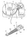
図1は、本発明の一実施形態として、磁気記録装置全体及びそのヘッドジンバルアセンブリ(HGA)を概略的に示す斜視図である。ここで、HGAの斜視図においては、HGAの磁気記録媒体表面に対向する側が上になって表示されている。 FIG. 1 is a perspective view schematically showing the entire magnetic recording apparatus and its head gimbal assembly (HGA) as one embodiment of the present invention. Here, in the perspective view of the HGA, the side facing the magnetic recording medium surface of the HGA is displayed with the side facing up.
同図に示した磁気記録装置としての磁気ディスク装置は、スピンドルモータ11の回転軸の回りを回転する、磁気記録媒体としての複数の磁気ディスク10と、複数の駆動アーム14が設けられたアセンブリキャリッジ装置12と、各駆動アーム14の先端部に取り付けられており、薄膜磁気ヘッドである熱アシスト磁気記録ヘッド21を備えたヘッドジンバルアセンブリ(HGA)17と、熱アシスト磁気記録ヘッド21の書き込み及び読み出し動作を制御し、さらに、後述する熱アシスト磁気記録用のレーザ光を発生させる光源であるレーザダイオードの発光動作を制御するための記録再生及び発光制御回路13とを備えている。 The magnetic disk apparatus as a magnetic recording apparatus shown in FIG. 1 is an assembly carriage provided with a plurality of
本実施形態において、磁気ディスク10は、垂直磁気記録用であり、ディスク基板に、軟磁性裏打ち層、中間層及び磁気記録層(垂直磁化層)が順次積層された構造を有している。アセンブリキャリッジ装置12は、熱アシスト磁気記録ヘッド21を、磁気ディスク10に形成されており記録ビットが並ぶトラック上に位置決めするための装置である。この装置内において、駆動アーム14は、ピボットベアリング軸16に沿った方向にスタックされており、ボイスコイルモータ(VCM)15によってこの軸16を中心にして角揺動可能となっている。なお、本発明に係る磁気ディスク装置の構造は、以上に述べた構造に限定されるものではない。磁気ディスク10、駆動アーム14、HGA17及びヘッド21は、単数であってもよい。 In the present embodiment, the
HGA17において、サスペンション20は、ロードビーム200と、このロードビーム200に固着されており弾性を有するフレクシャ201と、ロードビーム200の基部に設けられたベースプレート202とを備えている。また、フレクシャ201上には、リード導体及びその両端に電気的に接続された接続パッドからなる配線部材203が設けられている。熱アシスト磁気記録ヘッド21は、各磁気ディスク10の表面に対して所定の間隔(浮上量)をもって対向するように、サスペンション20の先端部であってフレクシャ201に固着されている。さらに、配線部材203の一端が、熱アシスト磁気記録ヘッド21の端子電極に電気的に接続されている。なお、サスペンション20の構造も、以上に述べた構造に限定されるものではない。図示されていないが、サスペンション20の途中にヘッド駆動用ICチップが装着されていてもよい。 In the
図2は、本発明による熱アシスト磁気記録ヘッド21の一実施形態を示す斜視図である。 FIG. 2 is a perspective view showing an embodiment of the thermally-assisted
同図によれば、熱アシスト磁気記録ヘッド21は、スライダ22及び光源ユニット23を備えている。スライダ22は、アルチック(Al2O3−TiC)、又は酸化シリコン(SiO2)等のセラミック材料から形成されており、適切な浮上量を得るように加工された媒体対向面である浮上面(ABS)2200を有するスライダ基板220と、ABS2200とは垂直であって隣り合った素子形成面2202上に形成されたヘッド素子部221とを備えている。また、光源ユニット23は、アルチック(Al2O3−TiC)、Si、GaAs、又はSiC等のセラミック材料又は半導体材料から形成されており、接合面2300を有するユニット基板230と、接合面2300とは垂直であって隣り合った光源設置面2302に設けられた光源としてのレーザダイオード40とを備えている。ここで、スライダ22と光源ユニット23とは、スライダ基板220の背面2201とユニット基板230の接合面2300とを合わせ、例えば半田を用いて互いに接着されている。ここで、スライダ基板220の背面2201は、スライダ基板220のABS2200とは反対側の端面に対応する。なお、熱アシスト磁気記録ヘッド21は、光源ユニット23を用いずに、レーザダイオード40がスライダ22に直接搭載された形態であってもよい。As shown in the figure, the heat-assisted
スライダ22のスライダ基板220の素子形成面2202上に形成されたヘッド素子部221は、磁気ディスクからデータを読み出すためのMR素子33と磁気ディスクにデータを書き込むための電磁変換素子34とから構成されるヘッド素子32と、光源ユニット23に備えられたレーザダイオード40からのレーザ光を媒体対向面側に導くための導波路35と、導波路35を伝播するレーザ光(導波路光)と表面プラズモンモードで結合し表面プラズモンを励起して近接場光を発生させるプラズモン発生素子36と、プラズモン発生素子36から発生する近接場光の光密度を向上させるために設けられた、共振器の反射鏡の役割を果たす共振鏡39と、MR素子33、電磁変換素子34、導波路35、プラズモン発生素子36、及び共振器39を覆うように素子形成面2202上に形成された保護層38と、保護層38の上面に露出しておりMR素子33に電気的に接続された一対の端子電極370と、同じく保護層38の上面に露出しており電磁変換素子34に電気的に接続された一対の端子電極371とを備えている。ここで、導波路35と、プラズモン発生素子36と、共振器39とが、熱アシストのための近接場光を発生させるプラズモン共振光学系31を構成する。また、端子電極370及び371は、フレクシャ201(図1)に設けられた配線部材203の接続パッドに電気的に接続される。 The
MR素子33、電磁変換素子34及びプラズモン発生素子36の一端は、ヘッド部221の媒体対向面であるヘッド端面2210に達している。ここで、ヘッド端面2210とABS2200とが熱アシスト磁気記録ヘッド21全体の媒体対向面をなしている。実際の書き込み又は読み出し時においては、熱アシスト磁気記録ヘッド21が回転する磁気ディスク表面上において流体力学的に所定の浮上量をもって浮上する。この際、MR素子33及び電磁変換素子34の端が、磁気ディスク10(図1)の磁気記録層の表面と適当なマグネティックスペーシングを介して対向することになる。この状態において、MR素子33が磁気記録層からのデータ信号磁界を感受して読み出しを行い、電磁変換素子34が磁気記録層にデータ信号磁界を印加して書き込みを行う。 One end of the
ここで、書き込みの際、光源ユニット23のレーザダイオード40から導波路35を通って伝播してきたレーザ光(導波路光)が、表面プラズモンモードでプラズモン発生素子36に結合し、プラズモン発生素子36に表面プラズモンを励起する。この励起された表面プラズモン(電磁場)は、プラズモン発生素子36の後述する伝播エッジ360(図4)上をヘッド端面2210に向けて伝播するが、同じく後に詳述するように、共振鏡39と磁気ディスク10の磁気記録層表面との間で共振する。その結果、プラズモン発生素子36のヘッド端面2210側の端において、非常に高い光密度を有する近接場光が発生する。この近接場光が磁気ディスク10に達し、磁気ディスクの磁気記録層部分を十分に加熱し、これにより、その部分の異方性磁界(保磁力)が書き込みを行うことが可能な値にまで十分に低下する。この異方性磁界が十分に低下した部分に電磁変換素子34によって書き込み磁界を印加することによって、良好な熱アシスト磁気記録を行うことが可能となるのである。 Here, at the time of writing, the laser light (waveguide light) propagating from the
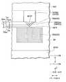
図3は、熱アシスト磁気記録ヘッド21の要部の構成を概略的に示す、図2のA面による断面図である。 FIG. 3 is a cross-sectional view taken along plane A of FIG. 2, schematically showing the configuration of the main part of the heat-assisted
図3によれば、MR素子33は、MR積層体332と、対となってMR積層体332及び絶縁層381を挟む位置に配置されている下部シールド層330及び上部シールド層334とを含み、素子形成面2202上に形成された絶縁層380上に形成されている。上下部シールド層334及び330は、MR積層体332が雑音となる外部磁界を受けることを防止する。また、MR積層体332は、MR効果を利用して信号磁界を感受する感磁部であり、例えば、面内通電型巨大磁気抵抗(CIP-GMR)効果を利用したCIP-GMR積層体、垂直通電型巨大磁気抵抗(CPP-GMR)効果を利用したCPP-GMR積層体、又はトンネル磁気抵抗(TMR)効果を利用したTMR積層体であってよい。これらのMR効果を利用したMR積層体332はいずれにおいても、高い感度で磁気ディスクからの信号磁界を感受する。なお、MR積層体332がCPP−GMR積層体又はTMR積層体である場合、上下部シールド層334及び330は、電極としての役割も果たす。 According to FIG. 3, the
同じく図3によれば、電磁変換素子34は、垂直磁気記録用であって、上部ヨーク層340と、主磁極3400と、書き込みコイル層343と、コイル絶縁層344と、下部ヨーク層345と、下部シールド3450とを備えている。 Similarly, according to FIG. 3, the
上部ヨーク層340は、コイル絶縁層344を覆うように形成されており、主磁極3400は、Al2O3(アルミナ)等の絶縁材料からなる絶縁層385内に形成されている。これら上部ヨーク層340及び主磁極3400は、互いに磁気的に接続されており、書き込みコイル層343に書き込み電流を印加することによって発生した磁束を、書き込みがなされる磁気ディスクの磁気記録層(垂直磁化層)まで収束させながら導くための導磁路となっている。このうち、主磁極3400は、ヘッド端面2210に達しており、主磁極3400のヘッド端面2210の一部をなす端面3400eにおいて、下部シールド3450に最も近い(最もリーディング側の)頂点が、書き込み磁界を発生させるポイント(WFP:図5)となっている。このように、主磁極3400が微小な書き込み磁界発生ポイントを有することによって、高記録密度化に対応した微細な書き込み磁界が発生可能となる。主磁極3400は、上部ヨーク層340よりも高い飽和磁束密度を有する軟磁性材料から形成されていることが好ましく、例えば、Feが主成分である鉄系合金材料である、FeNi、FeCo、FeCoNi、FeN又はFeZrN等の軟磁性材料から形成される。主磁極3400の厚さは、例えば、0.1〜0.8μm(マイクロメートル)とすることができる。The
書き込みコイル層343は、絶縁層385上に形成されたAl2O3(アルミナ)等の絶縁材料からなる絶縁層3421上において、1ターンの間に少なくとも下部ヨーク層345と上部ヨーク層340との間を通過するように形成されており、バックコンタクト部3402を中心として巻回するスパイラル構造を有している。この書き込みコイル層343は、例えばCu(銅)等の導電材料から形成されている。ここで、例えば加熱キュアされたフォトレジスト等の絶縁材料からなる書き込みコイル絶縁層344が、書き込みコイル層343を覆っており、書き込みコイル層343と上部ヨーク層340との間を電気的に絶縁している。書き込みコイル層343は、本実施形態において1層であるが、2層以上でもよく、又は上部ヨーク層340を間に挟むように配置されたヘリカルコイルでもよい。さらに、巻き数も図3に示す数に限定されるものではなく、例えば、2〜7ターンに設定され得る。The
なお、バックコンタクト部3402には、X軸方向に伸長した貫通孔が設けられており、この貫通孔の中を、導波路35及び導波路35を被覆する絶縁層が通り抜けている。この貫通孔内においては、バックコンタクト部3402の内壁と導波路35とが所定の距離、例えば少なくとも1μm離隔している。これにより、バックコンタクト部3402による導波路光の吸収が防止される。 The
下部ヨーク層345は、Al2O3(アルミナ)等の絶縁材料からなる絶縁層383上に形成されており、磁気ディスク10(図1)の磁気記録層(垂直磁化層)の下に設けられた軟磁性裏打ち層から戻ってきた磁束を導く導磁路としての役割を果たす。下部ヨーク層345は軟磁性材料から形成されており、その厚さは、例えば、0.5〜5μm程度である。また、下部シールド3450は、下部ヨーク層345と磁気的に接続されていてヘッド端面2210に達した磁気シールドである。下部シールド3450は、プラズモン発生素子36から見て主磁極3400とは反対側に設けられていて、プラズモン発生素子36を介して主磁極3400と対向しており、主磁極3400から発して広がった磁束を取り込む役割を果たす。なお、下部シールド3450は、高飽和磁束密度を有する、NiFe(パーマロイ)又は主磁極3400と同様の鉄系合金材料等から形成されることが好ましい。The
同じく図3によれば、導波路35、プラズモン発生素子36及び共振鏡39は、下部ヨーク層345(下部シールド3450)と上部ヨーク層340(主磁極3400)との間に設けられており、ヘッド素子部221内における近接場光を発生させるプラズモン共振光学系31をなす。ここで、導波路35は、素子形成面2202と平行であってヘッド部後端面2212の一部をなす後端面352からヘッド端面2210側の端面350まで伸長している。また、導波路35の上面(側面)の一部とプラズモン発生素子36の(伝播エッジ360を含む)下面の一部とは、所定の間隔をもって対向しており、これらに挟まれた絶縁層部分は、導波路35の屈折率よりも低い屈折率を有する緩衝部50となっている。この緩衝部50は、導波路35を伝播するレーザ光(導波路光)を、表面プラズモンモードでプラズモン発生素子36に結合させる役割を果たす。 Similarly, according to FIG. 3, the
プラズモン発生素子36は、導波路35と主磁極3400との間に位置しており、ヘッド端面2210の一部をなす近接場光発生端面36aを備えている。さらに、このプラズモン発生素子36は、少なくとも一部が緩衝部50を挟んで導波路35と対向しており近接場光発生端面36aまで伸長した伝播エッジ360であって、導波路35を伝播してきた導波路光によって励起される表面プラズモンを伝播させるための伝播エッジ360を備えている。このように、プラズモン発生素子36は、導波路光と表面プラズモンモードで結合して表面プラズモンを励起させ、この表面プラズモンを伝播エッジ360上に伝播させて、近接場光発生端面36aから近接場光を発生させる。 The
共振鏡39は、プラズモン発生素子36の近接場光発生端面36aとは反対側(+X側)に設けられており、励起された表面プラズモンを反射する役割を果たす。これにより、伝播エッジ360上を伝播する表面プラズモン(電磁場)は、共振鏡39と磁気ディスク10の磁気記録層表面との間で共振し、定常波をなす。その結果、表面プラズモンの振幅が増大し、プラズモン発生素子36の近接場光発生端面36aから非常に高い光密度を有する近接場光を発生させることが可能となる。 The
さらに、主磁極3400は、プラズモン発生素子36における伝播エッジ360を含まない表面部分と接面している。即ち、主磁極3400と伝播エッジ360とは、所定の間隔をもって離隔している。その結果、伝播エッジ360を伝播する表面プラズモンの多くが磁性金属材料で形成された主磁極3400に吸収され、プラズモン共振光学系31の光利用効率が大幅に低下する、という事態を回避することができる。なお、これら導波路35、プラズモン発生素子36、共振鏡39、及び主磁極3400の構成については、後に図4〜図6を用いて詳細に説明を行う。 Further, the main
同じく図3によれば、光源ユニット23は、ユニット基板230の光源設置面2302に設けられたレーザダイオード40と、レーザダイオード40の下面をなす下部電極40iに電気的に接続された端子電極410と、レーザダイオード40の上面をなす上部電極40aに電気的に接続された端子電極411とを備えている。これらの端子電極410及び411は、フレクシャ201(図1)に設けられた配線部材203の接続パッドに電気的に接続されている。この両電極410及び411を介してレーザダイオード40に所定の電圧を印加すると、レーザダイオード40の発光面400に位置する発光中心4000からレーザ光が放射される。ここで、図3に示されるようなヘッド構造において、レーザダイオード40が発生させるレーザ光の電場の振動方向が、活性層40eの積層面に対して垂直(Z軸方向)であることが好ましい。即ち、レーザダイオード40が発生させるレーザ光がTMモードの偏光であることが好ましい。これにより、導波路35を伝播するレーザ光が、緩衝部50を介して、表面プラズモンモードでプラズモン発生素子36に結合可能となる。 Similarly, according to FIG. 3, the
レーザダイオード40としては、InP系、GaAs系、GaN系等の、通信用、光学系ディスクストレージ用又は材料分析用等として通常用いられているものが使用可能であり、放射されるレーザ光の波長λLは、例えば375nm(ナノメートル)〜1.7μmの範囲内の値とすることができる。レーザダイオード40は、上部(n型)電極40aと、活性層40eと、下部(p型)電極40iとを含む多層構造を有している。この多層構造の劈開面の前後には、全反射による発振を励起するための反射層が形成されている。ここで、レーザダイオード40の厚さTLAは、例えば60〜200μm程度とすることができる。As the
また、このレーザダイオード40の駆動においては、磁気ディスク装置内の電源が使用可能である。実際、磁気ディスク装置は、通常、例えば2〜5V程度の電源を備えており、レーザ発振動作には十分の電圧を有している。また、レーザダイオード40の消費電力も、例えば、数十mW程度であり、磁気ディスク装置内の電源で十分に賄うことができる。なお、レーザダイオード40及び駆動端子電極410及び411は、上述した実施形態に限定されるものではない。例えば、レーザダイオード40において電極の上下を逆にし、n型電極40aがユニット基板230の光源設置面2302に接着されてもよい。また、熱アシスト磁気記録ヘッド21の素子形成面2202上にレーザダイオードを設置して、このレーザダイオードと導波路35とを光学的に接続することも可能である。また、熱アシスト磁気記録ヘッド21がレーザダイオード40を備えておらず、磁気ディスク装置内に設けられたレーザダイオードの発光中心と導波路35の後端面352とが、例えば光ファイバ等を用いて接続されていてもよい。 In driving the
また、スライダ22及び光源ユニット23の大きさは任意であるが、例えば、スライダ22は、トラック幅方向(Y軸方向)の幅700μm×(Z軸方向の)長さ850μm×(X軸方向の)厚さ230μmの、いわゆるフェムトスライダであってもよい。この場合、光源ユニット23は、これよりも一回り小さい大きさ、例えば、トラック幅方向の幅425μm×長さ300μm×厚さ300μmであってもよい。 The size of the
以上に述べた光源ユニット23とスライダ22とを接続することによって、熱アシスト磁気記録ヘッド21が構成される。この接続においては、ユニット基板230の接合面2300とスライダ基板220の背面2201とが接着されるが、その際、レーザダイオード40から発生したレーザ光が導波路35におけるABS2200とは反対側の後端面352に丁度入射するように、ユニット基板230及びスライダ基板220の位置が決定される。 The heat-assisted
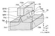
図4は、導波路35、プラズモン発生素子36、共振鏡39、及び主磁極3400の構成を概略的に示す斜視図である。同図においては、書き込み磁界及び近接場光が磁気記録媒体に向かって放射される位置を含むヘッド端面2210が、左側に位置している。 FIG. 4 is a perspective view schematically showing configurations of the
図4によれば、プラズモン共振光学系31として、近接場光発生用のレーザ光53を伝播させるための導波路35と、この導波路35とプラズモン発生素子36の伝播面(下面)361sとの間に挟まれた部分である緩衝部50と、レーザ光(導波路光)53と緩衝部50を介して表面プラズモンモードで結合し、表面プラズモンを励起させて伝播エッジ360上で伝播させ、ヘッド端面2210側の近接場光発生端面36aから近接場光を発生させるプラズモン発生素子36と、この伝播する表面プラズモンを反射する役割を果たす共振鏡39とが設けられている。 According to FIG. 4, the plasmon resonance
プラズモン発生素子36の伝播エッジ360は、少なくとも一部が緩衝部50を挟んで導波路35と対向しており、ヘッド端面2210とは反対側の端360sから近接場光発生端面36aの頂点NFPまで伸長している。この伝播エッジ360は、レーザ光(導波路光)53によって励起される表面プラズモンを近接場光発生端面36aまで伝播させる役割を果たす。 The
共振鏡39は、プラズモン発生素子36の近接場光発生端面36aとは反対側(+X側)に設けられている。この共振鏡39は、データ書き込み時に、頂点NFP(近接場光発生端面36a)と対向する磁気ディスク10(図1)の磁気記録層の表面部分を一方の鏡とした共振器における、他方の鏡としての役割を果たす。即ち、共振鏡39とこの磁気ディスク10の磁気記録層の表面部分とは、プラズモン発生素子36をその間に挟んだファブリペロー共振器を構成する。 The
ファブリペロー共振器は、光(電磁場)が伝播する経路の両端それぞれに反射鏡を設け、反射鏡の反射面同士を対向させた共振器である。例えば、レーザ装置は、レーザ媒質をこのファブリペロー共振器内に設置して構成されることができる。誘導放出されたレーザ光は、ファブリペロー共振器によって反射しレーザ媒質中を往復することによって、増幅され、特にファブリペロー共振器内で共振し定常波を形成している場合に、その振幅を増大させる。これにより、より高い強度のレーザ光を得ることができる。 A Fabry-Perot resonator is a resonator in which reflecting mirrors are provided at both ends of a path through which light (electromagnetic field) propagates, and reflecting surfaces of the reflecting mirrors face each other. For example, the laser device can be configured by installing a laser medium in the Fabry-Perot resonator. The stimulated emission of the laser light is amplified by being reflected by the Fabry-Perot resonator and reciprocating in the laser medium, and in particular, when it resonates in the Fabry-Perot resonator and forms a standing wave, its amplitude is increased. . Thereby, higher intensity laser light can be obtained.
図4においては、励起された表面プラズモン(電磁場)は、共振鏡39と磁気ディスク10の磁気記録層の表面部分とで反射して、プラズモン発生素子36の伝播エッジ360上を−X軸方向及び+X軸方向に往復し、その振幅を増大させる。特に、後に実施例を用いて詳述するように、プラズモン発生素子36の長さLPLを、次式
(λ0・m/(2・nEFFPG))−0.275・(λ0/(2・nEFFPG))≦LPL≦(λ0・m/(2・nEFFPG))+0.275・(λ0/(2・nEFFPG)) (1)
を満たすように設定してやることによって、励起された表面プラズモンは、共振鏡39と磁気記録層の表面部分とがなす共振器内で共振して定常波を形成し、その振幅を増大させるのである。ここで、λ0はレーザ光53の真空中での波長であり、nEFFPGは、表面プラズモンがプラズモン発生素子36の伝播エッジ360を表面プラズモンモードで伝播する際の実効屈折率であり、mは定常波の腹の数(自然数)である。In FIG. 4, the excited surface plasmon (electromagnetic field) is reflected by the
By setting so as to satisfy the above, the excited surface plasmon resonates in the resonator formed by the
これにより、プラズモン発生素子36の長さLPLを大きくせずに、プラズモン共振光学系31においてより高い光利用効率を得ることが可能となる。実際、この光利用効率を高める方法として、導波路光53をプラズモン発生素子36と表面プラズモンモードで十分に強く結合させるべく、プラズモン発生素子36の長さLPLをより大きく設定することが挙げられる。しかしながら、この場合、励起された表面プラズモンが、プラズモン発生素子36のより長い伝播経路を伝播する間に、金属で形成されているプラズモン発生素子36により多く吸収されてしまう。これにより、近接場光を発生させる表面プラズモンの量が減少し、結局、光利用効率が低下してしまうことが起こり得る。また、表面プラズモンを吸収したプラズモン発生素子36の温度が増大し、場合によってはプラズモン発生素子36が溶融する恐れも生じる。Thus, without increasing the length LPL of the
これに対して、本発明によるプラズモン共振光学系31においては、プラズモン発生素子36の長さLPLを大きくせずに、プラズモン発生素子36による表面プラズモンの吸収を、さらにはプラズモン発生素子36の過熱を抑制しつつ、共振器構造を用いて励起された表面プラズモンを増幅し、より高い光利用効率を得ることが可能となる。その結果、プラズモン発生素子36の近接場光発生端面36aから非常に高い光密度を有する近接場光を発生させることが可能となるのである。実際、後に示す実施例では、長さLPL=1.2〜1.3μmであるプラズモン発生素子36を含む共振器構造を有していない光学系において得られる近接場光の光密度を、24%上回る光密度を有する近接場光が、長さLPL=0.8μmのプラズモン発生素子36で実現されることが示されている。In contrast, in the plasmon resonance
なお、データ書き込み時において、近接場光の発生ポイントとなる頂点NFPは、磁気ディスク10と、浮上量に相当する距離dFH(図6)をもって対向する。従って、厳密には、上述した式(1)が表す関係にはこの距離dFHが勘案されなければならない。しかしながら、この距離dFHは、例えば数nm程度の非常に小さい値をとり、プラズモン発生素子36の長さLPLに比べて桁違いに小さい。このことから、距離dFHを含まない式(1)を、実質的に定常波を発生させる条件式として用いることができるのである。また一方で、図4に示すように、伝播エッジ360の端360bは、この共振鏡39の反射面390に突き当たっていることが好ましい。これにより、表面プラズモンは伝播エッジ360上を伝播したまま反射面390で反射されるので、表面プラズモンが伝播エッジ360から離脱することによる伝播損失が生じずに済む。At the time of data writing, the vertex NFP that is the generation point of near-field light faces the
また、主磁極3400は、プラズモン発生素子36における伝播エッジ360を含まない表面部分と接面している。この表面部分は、プラズモン発生素子36の伝播エッジ360を含む伝播面(下面)361sとは反対側の表面部分となる。これにより、主磁極3400と伝播エッジ360とは、所定の間隔をもって確実に離隔していることになる。その結果、伝播エッジ360を伝播する表面プラズモンの多くが磁性金属材料で形成された主磁極3400に吸収され、プラズモン共振光学系31の光利用効率が大幅に低下する、という事態を回避することができる。従って、励起された表面プラズモンは、主磁極3400にほとんど吸収されることなく、この伝播エッジ360に集中して伝播することができる。その結果、近接場光発生端面36aにおける1つの頂点であって伝播エッジ360の終端である頂点NFPが、確実に表面プラズモンが伝播して行き着く先となり、プラズモン発生素子36の近接場光の発生ポイントとなる。なお、伝播エッジ360の角は、表面プラズモンが伝播エッジ360から離脱して光利用効率が低下する現象を防止するために丸められている。この丸められた角の曲率半径は、6.25〜20nmの範囲内に設定されることが好ましいことが分かっている。 The main
さらに、同じく図4において、主磁極3400は、導波路35に向かって突出した突出部分3400aを有している。プラズモン発生素子36は、この突出部分3400aの突出端である磁極エッジ3400bの少なくともヘッド端面2210側の部分を覆っており、図4の実施形態において、断面がV字状である形状となっている。ここで、後に図5に示すように、磁極エッジ3400bのヘッド端面2210側の端WFPは、書き込み磁界の発生ポイントとなっている。従って、主磁極3400とプラズモン発生素子36とをこのような構成にすることによって、この書き込み磁界の発生ポイントWFPと、伝播エッジ360の終端である近接場光の発生ポイントNFPとの距離DWN(図5)を、プラズモン発生素子36のZ軸方向の厚さの調整によって所望の小さな値に設定することが可能となる。Further, in FIG. 4, the main
さらに、プラズモン発生素子36は、主磁極3400と接面している。これにより、プラズモン発生素子36が近接場光を発生させる際に生じる熱の一部を、主磁極3400に逃がすことができる。即ち、主磁極3400をヒートシンクとして用いることができる。その結果、プラズモン発生素子36の過度の温度上昇を抑制し、近接場光発生端面36aの不要な突出やプラズモン発生素子36における光利用効率の大幅な低下の回避に貢献することができる。さらに、プラズモン発生素子36は、同じく金属材料からなる主磁極3400と接していることによって、電気的に孤立した状態ではなくなる。その結果、プラズモン発生素子36からの静電気放電(ESD)による悪影響が抑制される。 Further, the
また、導波路35の側面(上面)354の一部分と、プラズモン発生素子36の伝播エッジ360を含む伝播面(下面)361sとの間に挟まれた部分が、緩衝部50となっている。即ち、伝播エッジ360は、緩衝部50に覆われている。この緩衝部50は、導波路光53を表面プラズモンモードでプラズモン発生素子36に結合させる役割を果たす。また、伝播エッジ360は、導波路光53によって緩衝部50を介して励起される表面プラズモンを近接場光発生端面36aまで伝播させる役割を果たす。なお、導波路35の側面とは、導波路35を取り囲む端面のうち、ヘッド端面2210側の端面350及びその反対側の後端面352以外の端面351、353及び354を指すものとする。この導波路35の側面は、コアに相当する導波路35及びクラッドに相当する周囲の保護層38(図2)において、伝播する導波路光53が全反射し得る面となる。ここで、緩衝部50は、保護層38の一部であってもよいし、保護層38とは別に設けられた新たな層であってもよい。 Further, a portion sandwiched between a part of the side surface (upper surface) 354 of the
プラズモン発生素子36は、Au(金)、Auを主成分とする合金、銀(Ag)、又はAgを主成分とする合金で形成されていることが好ましい。このうちAg合金は、特に、パラジウム(Pd)、Au、銅(Cu)、ルテニウム(Ru)、ロジウム(Rh)及びイリジウム(Ir)のグループから選択された少なくとも1つの元素を含むことが好ましい。プラズモン発生素子36をこのようなAg合金材料で形成した場合、理論的に最高の近接場光発生効率を示す材料であるAgに次ぐ、高い近接場光発生効率を実現した上で、クラック、チッピング(欠け)等の欠陥の発生が十分に抑制された伝播エッジ360を得ることが可能となる。なお、プラズモン発生素子36のトラック幅方向(Y軸方向)の幅WNF及び(Z軸方向の)厚さTNFは、レーザ光53の波長よりも小さい値に設定されることが好ましい。The
共振鏡39は、プラズモン発生素子36を伝播する表面プラズモン(電磁場)がその反射面390において高い反射率で反射するように、Ag、Cu等の金属材料から形成されることができる。また、この共振鏡39の(X軸方向の)厚さtREを、例えば5〜300nmの範囲内の値とすることにより、十分な厚さtREの下、十分に高い反射率が確保可能となる。The
また、導波路35の側面、即ち上面354、下面353、及びトラック幅方向(Y軸方向)の両側面351は、緩衝部50と接面した部分を除いて、保護層38(図2)、即ち絶縁層384及び385(図3)と接面している。ここで、導波路35は、保護層38の構成材料の屈折率nOCよりも高い屈折率nWGを有する、例えば誘電材料から形成されている。例えば、レーザ光53の波長が600nmであって、保護層38がAl2O3(n=1.63)から形成されている場合、導波路35は、SiOXNY(n=1.7〜1.85)、TaOX(n=2.16)、NbOX(n=2.33)、TiOX(n=2.3〜2.55)から形成されていてもよい。導波路35をこのような材料で形成することによって、材料そのものが有する良好な光学特性によってレーザ光53の伝播損失が低く抑えられる。さらに、導波路35がコアとして働く一方、保護層38がクラッドとしての機能を果たし、全側面での全反射条件が整うことになる。これにより、より多くのレーザ光(導波路光)53が緩衝部50の位置に達し、導波路35の伝播効率が向上する。なお、本実施形態において、導波路35(緩衝部50)と対向していない伝播エッジ360の部分は、屈折率nOCの保護層38の構成材料、例えば絶縁層385の一部3850によって覆われていてもよい。Further, the side surfaces of the
さらに、導波路35の形状については、トラック幅方向(Y軸方向)の幅が一定であってもよいが、図4に示すように、ヘッド端面2210側の部分のトラック幅方向(Y軸方向)の幅が狭くなっていてもよい。導波路35のヘッド端面2210側(端面350側)の部分におけるトラック幅方向(Y軸方向)の幅WWGは、例えば例えば0.3〜100μm程度とすることができ、(Z軸方向の)厚さTWGは、例えば0.1〜4μm程度とすることができる。Furthermore, as for the shape of the
緩衝部50は、導波路35の屈折率nWGよりも低い屈折率nBFを有する、例えば誘電材料で形成されている。例えば、レーザ光の波長が600nmであって、導波路35が、TaOX(n=2.16)から形成されている場合、緩衝部50は、SiO2(n=1.46)又はAl2O3(n=1.63)から形成されていてもよい。これらの場合、この緩衝部50を、SiO2又はAl2O3からなるクラッドとしての保護層38(図2)の一部とすることも可能である。また、緩衝部50の(Z軸方向の)厚さTBFは、10〜200nmであることが好ましい。また、導波路35の上面(側面)354と伝播面361s(伝播エッジ360)とに挟まれた部分である緩衝部50の(X軸方向の)長さLBFも、本発明による共振鏡39を用いることによって、共振鏡39を用いない場合に比べて十分に小さい値に設定可能となる。なお、後に示す実施例においては、緩衝部50の長さLBFがプラズモン発生素子36の長さLPLに等しい構成が示されている。これら緩衝部50の長さLBF及び厚さTBFは、表面プラズモンの適切な励起、伝播を得るために重要なパラメータとなる。The
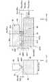
図5は、導波路35、プラズモン発生素子36、及び電磁変換素子34の、ヘッド端面2210上又はその近傍での端面の形状を示す平面図である。 FIG. 5 is a plan view showing the shapes of the end surfaces of the
同図に示すように、電磁変換素子34においては、主磁極3400と下部シールド3450とがヘッド端面2210に達している。このうち、主磁極3400のヘッド端面2210上における端面3400eは、例えば実質的に長方形、正方形又は台形のトレーリング側の部分と、導波路35に向かって突出した突出部分3400aの端面3400aeとが連結した形状を有している。ここで、端面3400e上における最もリーディング側の頂点WFPは、下部シールド3450に最も近いことから磁界が最も集中する個所であり、書き込み磁界の発生ポイントとなっている。このように、主磁極3400が微小な書き込み磁界発生ポイントを有することによって、高記録密度化に対応した微細な書き込み磁界が発生可能となる。 As shown in the figure, in the
また、ヘッド端面2210上において、プラズモン発生素子36の近接場光発生端面36aは、所定の厚さを持ったV字状の形状を有しており、主磁極3400の端面3400eは、この近接場光発生端面36aと接している。このような端面3400eと端面36aとの配置によって、書き込み磁界の発生ポイントWFPと、伝播エッジ360のヘッド端面2210側の端である近接場光の発生ポイントNFPとが、プラズモン発生素子36(近接場光発生端面36a)のZ軸方向での厚さに相当する距離DWNだけ離隔することになる。従って、近接場光発生端面36aの厚さを適切な微小値に制御することによって、書き込み磁界の発生ポイントWFPと近接場光の発生ポイントNFPとを十分に近接させることができる。その結果、磁気ディスク10上の近接場光を照射した位置において、主磁極3400からの書き込み磁界の磁界勾配を十分に大きくすることができ、高記録密度に対応した熱アシスト磁気記録が実施可能となる。なお、製造現場において、両ポイントWFP及びNFP間の距離DWNは、磁気ディスク10の磁気記録層上の近接場光を照射した位置における書き込み磁界の磁界勾配を十分に大きくし高記録密度に対応した熱アシスト磁気記録が実施可能とするために、30nm以上であって100nm以下であることが好ましいことが分かっている。On the
また、主磁極3400の突出していない部分(突出部分3400a以外の部分)と導波路35との間の距離DMWを所定量確保することによって、導波路光の一部が金属材料からなる主磁極3400に吸収されてしまって近接場光に変換される光量が低減してしまう事態を回避することができる。この距離DMWは、
DMW=t3400a+DWN+TBF (2)
となる。ここで、t3400aは、主磁極3400の突出部分3400aのZ軸方向での厚さであり、TBFは、近接場光発生ポイントNFPと導波路35とのZ軸方向での距離、即ち緩衝部50(図4)の厚さである。この厚さTBFは、表面プラズモンの適切な励起、伝播を得るために所定値に設定される。従って、式(1)から理解されるように、厚さt3400aを十分に大きく設定することによって、両ポイントWFP及びNFP間の距離DWNを十分に小さな値に設定した上で、距離DMWを所定量確保することが可能となるのである。Also, do not project of the main
DMW = t3400a + DWN + TBF (2)
It becomes.Here, t 3400a is the thickness in the Z axis direction of the protruding
以上述べたように、本発明による熱アシスト磁気記録ヘッドにおいては、ヘッド端面2210上において、書き込みの際に加熱作用部分となるポイントNFPと、書き込み作用部分となるポイントWFPとの間の距離DWNが、十分に小さい値に設定可能となる。これにより、磁気ディスクの磁気記録層において十分に加熱した部分に、十分に大きな勾配を有する書き込み磁界を印加することができる。その結果、高記録密度に対応した非常に微細な記録ビットを形成することが可能となる。As described above, in the thermally-assisted magnetic recording head according to the present invention, on the
図6は、本発明に係る表面プラズモンモードを利用した熱アシスト磁気記録を説明するための概略図である。 FIG. 6 is a schematic diagram for explaining heat-assisted magnetic recording using the surface plasmon mode according to the present invention.
同図によれば、電磁変換素子34による磁気ディスク10の磁気記録層への書き込みの際、最初に、光源ユニット23のレーザダイオード40から放射されたレーザ光53が、導波路35を伝播する。次いで、緩衝部50の近傍まで進行したレーザ光(導波路光)53は、屈折率nWGを有する導波路35と、屈折率nBFを有する緩衝部50と、金属等の導電材料からなるプラズモン発生素子36との光学的構成と結びついて、プラズモン発生素子36に表面プラズモンモードを誘起する。即ち、表面プラズモンモードでプラズモン発生素子36に結合する。According to the figure, when writing to the magnetic recording layer of the
実際には、コアである導波路35と緩衝部50との光学的な界面条件から、緩衝部50内にエバネッセント光が励起される。次いで、このエバネッセント光と、プラズモン発生素子36の金属表面(伝播エッジ360)に励起される電荷のゆらぎとが結合する形で表面プラズモンモードが誘起され、表面プラズモンが励起される。なお、正確には、この系においては素励起である表面プラズモンが電磁場と結合することになるので、励起されるのは表面プラズモン・ポラリトンである。しかしながら以後、省略して、表面プラズモン・ポラリトンを表面プラズモンと呼ぶ。以上に述べた表面プラズモンモードの誘起は、緩衝部50の屈折率nBFを導波路35の屈折率nWGよりも小さく設定し(nBF<nWG)、さらに、緩衝部50の(X軸方向の)長さ、即ち導波路35とプラズモン発生素子36との結合部分の長さLBFと、緩衝部50の(Z軸方向の)厚さTBFとを適切に選択することによって可能となる。Actually, evanescent light is excited in the
ここで、プラズモン発生素子36の伝播エッジ360は、導波路35と対向する伝播面(下面)361sにおいて導波路35に最も近い位置にあり、また角部であって電場が集中しやすい。その結果、表面プラズモンは、この伝播エッジ360に最も強く励起される。この励起された表面プラズモン60は、主にこの伝播エッジ360上を矢印61の方向に沿って伝播し、ヘッド端面2210の一部をなす近接場光発生端面36aの頂点NFPに達し、その結果、この頂点NFPから近接場光62が発生する。 Here, the
この近接場光62の一部は、磁気ディスク10の磁気記録層100の表面100aで反射し、電磁波62rとして伝播エッジ360に戻り、伝播エッジ360上を表面プラズモン60rとして矢印61rの方向に沿って伝播する。この表面プラズモン60rが共振鏡39の反射面390で反射し、伝播エッジ360上を再び表面プラズモン60として矢印61の方向に沿って伝播する。このように、励起された表面プラズモン(電磁場)は、共振鏡39と磁気ディスク10の磁気記録層100の表面100aとで反射して、伝播エッジ360上を矢印61の方向及び矢印61rの方向に往復し、その結果、その強度が増幅される。特に、後に実施例を用いて詳述するように、プラズモン発生素子36の長さLPLを、上述した式(1)に示したように、λ0・m/(2・nEFFPG)を中心としてこの中心から±0.275・λ0/(2・nEFFPG)以内の範囲内の値に設定することによって、励起された表面プラズモンは、共振鏡39と磁気記録層100の表面100aとがなす共振器内で共振して定常波600を形成する。その結果、表面プラズモンの振幅が増大するのである。これにより、近接場光62の光密度が向上し、磁気記録層100に十分な強度と微細なスポットサイズを有する近接場光が照射可能となるのである。これにより、磁気記録層100の照射された微小部分の異方性磁界(保磁力)が書き込みを行うことが可能な値にまで十分に低下する。その直後、この部分に、主磁極3400の端面3400eの頂点WFPから発生する書き込み磁界63を印加して書き込みを行う。以上により、良好な熱アシスト磁気記録を行うことが可能となる。A part of the near-
ここで、従来の、導波路を伝播するレーザ光がヘッド端面の位置に設けられた近接場光発生素子に直接照射される形態においては、照射されたレーザ光の多くの部分が、近接場光発生素子内で熱エネルギーに変わってしまう。この近接場光発生素子のサイズはレーザ光の波長以下に設定されており、その体積は非常に小さい。従って、この熱エネルギーによって、近接場光発生素子は非常な高温、例えば500℃にまで達していた。その結果、近接場光発生素子が熱膨張して読み出しヘッド素子の媒体対向面に達した端が相対的に磁気ディスクから遠ざかってしまい、記録動作時にサーボ信号を良好に読み出すことが困難となることが問題となっていた。さらに、近接場光発生素子内の自由電子の熱擾乱が大きくなって光利用効率を大幅に劣化させてしまうことも問題となっていた。 Here, in the conventional form in which the laser light propagating through the waveguide is directly applied to the near-field light generating element provided at the position of the head end face, a large part of the irradiated laser light is generated by the near-field light. It turns into thermal energy in the generating element. The size of the near-field light generating element is set to be equal to or less than the wavelength of the laser light, and its volume is very small. Therefore, the near-field light generating element has reached a very high temperature, for example, 500 ° C. by this thermal energy. As a result, the near-field light generating element thermally expands and the end of the read head element that reaches the medium facing surface moves away from the magnetic disk relatively, making it difficult to read the servo signal well during the recording operation. Was a problem. Furthermore, there has been a problem that the thermal disturbance of free electrons in the near-field light generating element is increased and the light utilization efficiency is greatly deteriorated.
これに対して、本発明による熱アシスト磁気記録においては、表面プラズモンモードを利用しており、表面プラズモン60及び60rを伝播エッジ360上で伝播させることによって近接場光62を発生させている。これにより、近接場光発生端面36aにおける近接場光発生時の温度が、例えば約100℃前後となり大幅に低減する。その結果、近接場光発生端面36aの磁気ディスク10に向かう方向の突出が抑制され、良好な熱アシスト磁気記録が可能となる。 On the other hand, in the heat-assisted magnetic recording according to the present invention, the surface plasmon mode is used, and the near-
図7a〜図7dは、本発明によるプラズモン共振光学系及び主磁極における種々の構成例を示す斜視図である。なお、図7dは、プラズモン発生素子88と主磁極89とを分離させた状態を表す斜視図となっている。 7a to 7d are perspective views showing various configuration examples of the plasmon resonance optical system and the main pole according to the present invention. FIG. 7d is a perspective view showing a state in which the
図7aによれば、表面プラズモン発生素子71は、導波路70及び主磁極72の間に設けられていて、絶縁層73によって周りを覆われており、導波路70とも主磁極72とも互いに離隔している。このプラズモン発生素子71は、絶縁層部分730を介して所定の間隔DBFをもって導波路70と対向した導波路対向面711を備えており、プラズモン発生素子71の伝播エッジ710は、この導波路対向面711とは反対側に位置している。このような図7aの構成例においては、導波路70と、絶縁層部分730と、表面プラズモン発生素子71とは、エバネッセント光を用いて表面プラズモンを励起するための光学系の一配置であるオットー(Otto)配置をなしている。オットー配置は、レーザ光が入射する側から、第1の誘電体領域、第1の誘電体領域の屈折率よりも小さな屈折率を有する第2の誘電体領域、及び金属領域が、隣同士互いに接して順次並んだ配置である。According to FIG. 7 a, the surface
この図7aの例においては、表面プラズモン発生素子71の導波路対向面711の近傍まで進行したレーザ光(導波路光)は、屈折率nWGを有する導波路70と、屈折率nOC(nOC<nWG)を有する緩衝部(絶縁層部分730、及び素子71を覆う絶縁層73)と、金属等の導電材料からなる表面プラズモン発生素子71との光学的構成と結びついて、表面プラズモン発生素子71に表面プラズモンモードを誘起する。即ち、導波路70からのしみ出し光と、表面プラズモン発生素子71の表面に励起される電荷のゆらぎとが結合する形で表面プラズモンモードが誘起され、伝播エッジ710に表面プラズモンが励起される。In the example of FIG. 7a, laser light (waveguide light) that hastraveled to the vicinity of the
さらに、図7aによれば、プラズモン発生素子71の近接場光発生端面71aとは反対側(+X側)には、共振鏡74が設けられている。この共振鏡74は、伝播エッジ710に励起された表面プラズモンを反射する役割を果たす。ここで、伝播エッジ710の近接場光発生端面71a(NFP)とは反対側の端710sは、共振鏡74の反射面740に突き当たっていることが好ましい。以上述べた構成によって、伝播エッジ710を伝播する表面プラズモン(電磁場)は、データ書き込み時において、共振鏡74と磁気ディスク10(図1)の磁気記録層表面との間で共振し、定常波をなす。その結果、プラズモン発生素子71の近接場光発生端面71a(NFP)から非常に高い光密度を有する近接場光を発生させることが可能となる。これにより、図7aの構成例においても、良好な熱アシスト磁気記録を行うことが可能となる。 Furthermore, according to FIG. 7 a, a
次いで、図7bの構成例によれば、表面プラズモン発生素子76は、導波路75及び主磁極77の間に設けられていて、絶縁層78によって周りを覆われており、導波路75とは接面していて、主磁極77とは互いに離隔している。このプラズモン発生素子76は、導波路75と接面した導波路接触面761を備えており、プラズモン発生素子76の伝播エッジ760は、この導波路接触面761とは反対側に位置している。このような図7bの構成例においては、導波路75と、表面プラズモン発生素子76と、絶縁層78とは、エバネッセント光を用いて表面プラズモンを励起するための光学系の一配置であるクレッチマン(Kretschmann)配置をなしている。クレッチマン配置は、レーザ光が入射する側から、第1の誘電体領域、金属領域、及び第1の誘電体領域の屈折率よりも小さな屈折率を有する第2の誘電体領域が、隣同士互いに接して順次並んだ配置である。 Next, according to the configuration example of FIG. 7 b, the surface
この図7bの構成例においては、表面プラズモン発生素子76の導波路接触面761の近傍まで進行したレーザ光(導波路光)は、屈折率nWGを有する導波路75と、金属等の導電材料からなる表面プラズモン発生素子76と、屈折率nOC(nOC<nWG)を有する緩衝部(素子76を覆う絶縁層78)との光学的構成と結びついて、表面プラズモン発生素子76に表面プラズモンモードを誘起する。即ち、導波路75からのしみ出し光と、表面プラズモン発生素子76の表面に励起される電荷のゆらぎとが結合する形で表面プラズモンモードが誘起され、伝播エッジ760に表面プラズモンが励起される。In the configuration example of FIG. 7b, laser light (waveguide light) that has traveled to the vicinity of the
さらに、図7bによれば、プラズモン発生素子76の近接場光発生端面76aとは反対側(+X側)には、共振鏡79が設けられている。この共振鏡79は、伝播エッジ760に励起された表面プラズモンを反射する役割を果たす。ここで、伝播エッジ760の近接場光発生端面76a(NFP)とは反対側の端760sは、共振鏡79の反射面790に突き当たっていることが好ましい。以上に述べた構成によって、伝播エッジ760を伝播する表面プラズモン(電磁場)は、データ書き込み時において、共振鏡79と磁気ディスク10(図1)の磁気記録層表面との間で共振し、定常波をなす。その結果、プラズモン発生素子76の近接場光発生端面76a(NFP)から非常に高い光密度を有する近接場光を発生させることが可能となる。これにより、図7bの構成例においても、良好な熱アシスト磁気記録を行うことが可能となる。 Furthermore, according to FIG. 7 b, a
次いで、図7cの構成例によれば、表面プラズモン発生素子81は、導波路80及び主磁極82の間に設けられていて、絶縁層83によって周りを覆われており、導波路80とも主磁極82とも互いに離隔している。このプラズモン発生素子81においては、伝播エッジ810の少なくとも一部が、絶縁層部分830を介して所定の間隔DBF′をもって導波路80と対向している。Next, according to the configuration example of FIG. 7 c, the surface
このような図7cの構成例においては、導波路80と、導波路80及び表面プラズモン発生素子81の間に介在する絶縁層部分830と、表面プラズモン発生素子81とは、図7aの構成例と同じく、オットー配置をなしている。ここで、表面プラズモン発生素子81の伝播エッジ810の近傍まで進行したレーザ光(導波路光)は、屈折率nWGを有する導波路80と、屈折率nOC(nOC<nWG)を有する緩衝部(絶縁層部分830、及び素子81を覆う絶縁層83)と、金属等の導電材料からなる表面プラズモン発生素子81との光学的構成と結びついて、表面プラズモン発生素子81の伝播エッジ810に表面プラズモンモードを誘起する。即ち、導波路80からのしみ出し光と、導波路80に最も近く電場が集中しやすい角をなす伝播エッジ810に励起される電荷のゆらぎとが結合する形で表面プラズモンモードが誘起され、表面プラズモンが伝播エッジ810に励起される。In the configuration example of FIG. 7c, the
さらに、図7cによれば、プラズモン発生素子81の近接場光発生端面81aとは反対側(+X側)には、共振鏡84が設けられている。この共振鏡84は、伝播エッジ810に励起された表面プラズモンを反射する役割を果たす。ここで、伝播エッジ810の近接場光発生端面81a(NFP)とは反対側の端810sは、共振鏡84の反射面840に突き当たっていることが好ましい。以上述べた構成によって、伝播エッジ810を伝播する表面プラズモン(電磁場)は、データ書き込み時において、共振鏡84と磁気ディスク10(図1)の磁気記録層表面との間で共振し、定常波をなす。その結果、プラズモン発生素子81の近接場光発生端面81aから非常に高い光密度を有する近接場光を発生させることが可能となる。これにより、図7cの構成例の実施形態においても、良好な熱アシスト磁気記録を行うことが可能となる。 Furthermore, according to FIG. 7 c, a
なお、近接場光発生端面81aの形状、サイズを調整することによって、プラズモン発生素子81における主磁極82の端面82e側の端辺NFEから集中して近接場光を発生させることも可能となる。これにより、この近接場光の発生領域となる端辺NFEと、書き込み磁界の発生領域となる主磁極82の端面82eの端辺WFEとを十分に近づけることが可能となる。その結果、磁気ディスク10の磁気記録層において十分に加熱した部分に、十分に大きな勾配を有する書き込み磁界を印加することができ、熱アシストによる安定した書き込み動作が確実に実施可能となる。 In addition, by adjusting the shape and size of the near-field light generating
次いで、図7dの構成例によれば、プラズモン発生素子88は、ヘッド端面2210に向かうにつれてトラック幅方向(Y軸方向)の幅が狭くなる受け皿状の形状を有している。また、主磁極89の突出部分89aは、このプラズモン発生素子88の受けの部分に隙間無く嵌っている。従って、主磁極89は、プラズモン発生素子88の受け皿の内壁と接面した形でプラズモン発生素子88と接触していることになる。 Next, according to the configuration example of FIG. 7d, the
プラズモン発生素子88は、さらに、導波路と対向する側に、伝播面880sと、先細となった伝播面880sの先端と連結されておりヘッド端面2210に達した伝播エッジ880とを備えている。励起された表面プラズモン86は、伝播面880s上をヘッド端面2210に向かって伝播して伝播エッジ880に集中し、さらに、この伝播エッジ880上を伝播して近接場光発生ポイントNFPに至る。 The
さらに、図7dによれば、プラズモン発生素子88の近接場光発生端面88aとは反対側(+X側)には、共振鏡87が設けられている。この共振鏡87は、伝播面880sに励起された表面プラズモンを反射する役割を果たす。ここで、伝播面880sの近接場光発生端面88a(NFP)とは反対側の端880ssは、共振鏡87の反射面870に突き当たっていることが好ましい。以上に述べた構成によって、伝播面880s及び伝播エッジ880を伝播する表面プラズモン(電磁場)は、データ書き込み時において、共振鏡87と磁気ディスク10(図1)の磁気記録層表面との間で共振し、定常波をなす。その結果、プラズモン発生素子88の近接場光発生端面88a(NFP)から非常に高い光密度を有する近接場光を発生させることが可能となる。これにより、図7dの構成例においても、良好な熱アシスト磁気記録を行うことが可能となる。 Further, according to FIG. 7d, a
以下、本発明による熱アシスト磁気記録ヘッドにおけるプラズモン共振光学系での近接場光の発生を、シミュレーションによって解析した実施例を示す。 Hereinafter, examples in which the generation of near-field light in the plasmon resonance optical system in the thermally-assisted magnetic recording head according to the present invention is analyzed by simulation will be shown.
シミュレーション解析実験は、電磁場解析である3次元の時間領域差分法(Finite−Difference Time−Domain(FDTD)法)を用いて行われた。図8は、実施例及び比較例としてのシミュレーション解析実験が行われた系を示す概略図である。同図に示すように、導波路90に入射させたレーザ光は、波長λLが800nmであって、TM偏光(レーザ光の電場の振動方向が導波路90の層面に垂直:Z軸方向)を有するガウシアンビームであった。また、このレーザ光の強度IINは、1.0(V/m)2であった。The simulation analysis experiment was performed using a three-dimensional time-domain difference method (Finite-Difference Time-Domain (FDTD) method) which is an electromagnetic field analysis. FIG. 8 is a schematic diagram showing a system in which simulation analysis experiments as examples and comparative examples were performed. As shown in the figure, the laser light incident on the
導波路90は、幅WWGが0.5μm、厚さTWGが0.4μmであり、TaOX(屈折率nWG=2.15)で形成されていた。また、表面プラズモン発生素子91は、Auで形成されており、その高さTNFが200nmであった。このAuにおいては、複素屈折率の実数部が0.2であって虚数部が4.88であった。また、表面プラズモン発生素子91のヘッド部端面2210上での近接場光発生ポイントNFPにおける頂角θNFは、45度(°)であった。さらに、伝播エッジ910の角の曲率半径は10nmであった。また、近接場光発生ポイントNFP(伝播エッジ910)と導波路90との距離TBFは、35nmであった。さらにまた、主磁極92はFeCoによって形成されていた。このFeCoにおいては、複素屈折率の実数部が3.08であって虚数部が3.9であった。さらに、導波路90、表面プラズモン発生素子91及び主磁極92を覆っており緩衝部となる部分を含む保護層93は、Al2O3(アルミナ:屈折率nBF=1.65)で形成されていた。The
表面プラズモン発生素子91の近接場光発生ポイントNFPと主磁極92の書き込み磁界発生ポイントWFPとの間の距離DWNは、35nmであった。この距離DWNは、表面プラズモン発生素子91のZ軸方向の厚さに相当する。また、本シミュレーション解析実験では、プラズモン発生素子91のZ軸方向の長さLPLを、0.75μm、0.78μm、0.8μm、0.82μm、0.87μmの値の範囲で変化させた。また、プラズモン発生素子91のヘッド端面2210(NFP)とは反対側(+X側)に、共振鏡94が設けられていた。ここで、伝播エッジ910の端910sが共振鏡94の反射面940に突き当たっていた。共振鏡94は、Auで形成されており、そのX軸方向の厚さtREが50nmであった。さらに、ヘッド端面2210上の近接場光発生ポイントNFPに対向して、磁気記録媒体95が設けられていた。磁気記録媒体95は、CoCrPtで形成されており、その表面950とNFPとのX軸方向での距離dFHは、6nmであった。The distance DWN between the near-field light generation point NFP of the surface
また、比較例として、共振鏡94が存在しないこと以外は以上に述べたプラズモン共振光学系と同じ構成を有する光学系のシミュレーション解析実験も行った。この比較例においては、プラズモン発生素子91のZ軸方向の長さLPLを、0.8μm、1.1μm、1.2μm、1.3μm、1.4μm、1.5μmの値の範囲で変化させた。As a comparative example, a simulation analysis experiment of an optical system having the same configuration as the plasmon resonance optical system described above was performed except that the
以上で述べた実験条件の下、プラズモン発生素子91の長さLPLと、表面プラズモン発生素子91の近接場光発生ポイントNFPから発生する近接場光の光密度max|E|2との関係をシミュレーションにより測定した。ここで、光密度max|E|2は、近接場光発生ポイントNFPから放射され、NFPから−X方向に6nm離れた位置にある磁気記録媒体95に達した近接場光における電界成分Eの絶対値の二乗のスポット内での最大値である。Under the experimental conditions described above, the relationship between the length LPL of the
表1は、共振鏡94が設けられた実施例における、プラズモン発生素子91の長さLPLと、近接場光発生ポイントNFPから発生する近接場光の光密度max|E|2との関係を示している。また、表2は、共振鏡94が設けられていない比較例における、プラズモン発生素子91の長さLPLと、近接場光発生ポイントNFPから発生する近接場光の光密度max|E|2との関係を示している。ここで、表1及び表2におけるNmax|E|2は、比較例(共振鏡94無し:表2)における長さLPL=1.2μmの場合での近接場光の光密度max|E|2を基準(100%)とした際の、規格化された光密度max|E|2(%)である。また、図9は、表面プラズモンが伝播エッジ910を表面プラズモンモードで伝播する際の実効屈折率nEFFPGを求めるためのグラフである。さらに、図10は、表1に示された実施例の結果、及び表2に示された比較例の結果を合わせて示すグラフである。なお、図10の縦軸は、上述したNmax|E|2(%)となっている。Table 1 shows the relationship between the length LPL of the

図10によれば、共振鏡94が設けられていない比較例(表2)において、Nmax|E|2のグラフは、プラズモン発生素子91の長さLPL=1.2、1.3μmにおける100%を極大として、ブロードなピークをなしている。ここで、Nmax|E|2が長さLPLに関して極大値を有することは、長さLPLが増加するとともに、表面プラズモンモードでの結合の度合いが大きくなる効果と、導波路90からプラズモン発生素子91に移り再び導波路90に戻るエネルギー分の増大との競合によるものと考えられる。これに対して、共振鏡94が設けられた実施例(表1)においては、Nmax|E|2のグラフは、プラズモン発生素子91の長さLPL=0.8μmにおける124%を最大として、よりシャープなピークをなしている。According to FIG. 10, in the comparative example (Table 2) in which the
本実施例において、このシャープなピークが共振に対応していることを以下に考察する。共振鏡94を設けることによって、伝播エッジ910上で伝播する表面プラズモンが共振し、腹の数がmである表面プラズモン(電磁場)の定常波が形成される場合のプラズモン発生素子91の長さをLPL(m)とすると、LPL(m)は、次式
LPL(m)=λ0・m/(2・nEFFPG) (3)
で表される。ここで、λ0は導波路90に入射したレーザ光の真空中での波長であり、nEFFPGは、表面プラズモンが伝播エッジ910を表面プラズモンモードで伝播する際の実効屈折率である。In the present embodiment, it will be considered below that this sharp peak corresponds to resonance. By providing the
It is represented by Here, λ0 is the wavelength of the laser light incident on the
ここで、図10において、共振鏡94が設けられた実施例において光密度max|E|2の最大値を与える長さLPL=0.8μmは、式(3)においてm=4、λ0=800nm、nEFFPG=2.001としたLPL(4)にほぼ相当する(LPL(4)=799.6nm)。即ち、共振鏡94が設けられた実施例における光密度max|E|2の最大値は、伝播エッジ910上に腹の数が4つである表面プラズモン(電磁場)の定常波が形成されたことによってこの表面プラズモンが増幅された結果得られたものであることが理解される。この光密度max|E|2の最大値(0.99(V/m)2)は、共振鏡94が設けられていない比較例での長さLPL=1.2、1.3μmにおける極大値(0.80(V/m)2)よりも24%向上している。即ち、共振器構造を有していない光学系において得られる近接場光の光密度を24%も上回る光密度を有する近接場光が、共振鏡94を設けることによって、長さLPLが62〜67%程度しかないプラズモン発生素子91において実現されることが分かる。Here, in FIG. 10, the length LPL = 0.8 μm that gives the maximum value of the optical density max | E |2 in the embodiment in which the
なお、式(3)に代入したnEFFPG値(2.001)は、図9に示したシミュレーション実験結果を用いて導出された。このシミュレーション実験では、導波路90、表面プラズモン発生素子91及び主磁極92を覆っている(緩衝部を含む)保護層93の屈折率nBFと、実効屈折率nEFFPGとの関係を計算した。その結果、屈折率nBF=1.45、1.65、1.8に対して、実効屈折率nEFFPGは、それぞれ、1.751、2.001、2.217となることが分かった。この結果をグラフにしたのが図9である。この図9によれば、屈折率nBFと実効屈折率nEFFPGとの間には、nEFFPG=1.328・nBF−0.1796との関係が存在している。本実施例においては、保護層93はAl2O3(nBF=1.65)であるので、この関係式から、nEFFPG=2.001が得られた。Note that the nEFFPG value (2.001) assigned to Equation (3) was derived using the simulation experiment results shown in FIG. In this simulation experiment, the relationship between the refractive index nBF of the protective layer 93 (including the buffer portion) covering the
さらに、図10によれば、共振鏡94が設けられた実施例におけるNmax|E|2のピークのNmax|E|2=100%でのピーク幅PW100は、0.11μmである。この値はまさに、腹の数が1つである表面プラズモン(電磁場)の定常波の長さ(λ0/(2・nEFFPG))(=0.200μm)の約55%(=27.5%×2)に相当する。従って、共振鏡94が設けられていない比較例での光密度の極大値以上の光密度max|E|2を得ることができるプラズモン発生素子91の長さLPLは、前述した式(1)Furthermore, according to FIG. 10, the peak width PW100 when Nmax | E |2 = 100% of the peak of Nmax | E |2 in the example in which the
(λ0・m/(2・nEFFPG))−0.275・(λ0/(2・nEFFPG))≦LPL≦(λ0・m/(2・nEFFPG))+0.275・(λ0/(2・nEFFPG)) (1)
で表現されることができる。式(1)を満たす長さLPLを有するプラズモン発生素子91を用いることによって、伝播エッジ910上に腹の数がmである表面プラズモン(電磁場)の定常波を形成することができ、結果として、より大きな長さLPLを必要とする比較例以上の光密度を有する近接場光を発生させることが可能となるのである。このように、プラズモン発生素子91の長さLPLは、式(1)を満たすことが好ましく、式(3)を満たすことがより好ましいことが理解される。(Λ0 · m / (2 · nEFFPG )) − 0.275 · (λ0 / (2 · nEFFPG )) ≦ LPL ≦ (λ0 · m / (2 · nEFFPG )) + 0.275 · (Λ0 / (2 · nEFFPG )) (1)
Can be expressed in By using a
以上、本発明によれば、表面プラズモンの吸収及び素子の過熱を抑制するためにプラズモン発生素子をより短くしつつ、共振器構造を用いることによって、励起された表面プラズモンを増幅し、より高い光密度を有する近接場光を発生させることが可能となることが理解される。また、その結果、より高い光利用効率を示すプラズモン共振光学系を実現でき、この系を用いてより高い記録密度に対応した熱アシスト磁気記録を実施することが可能となる。 As described above, according to the present invention, the excited surface plasmon is amplified by using the resonator structure while shortening the plasmon generating element in order to suppress the absorption of the surface plasmon and the overheating of the element, thereby increasing the light intensity. It will be understood that near-field light having a density can be generated. As a result, a plasmon resonance optical system exhibiting higher light utilization efficiency can be realized, and heat-assisted magnetic recording corresponding to a higher recording density can be performed using this system.
以上述べた実施形態は全て本発明を例示的に示すものであって限定的に示すものではなく、本発明は他の種々の変形態様及び変更態様で実施することができる。従って本発明の範囲は特許請求の範囲及びその均等範囲によってのみ規定されるものである。 All the embodiments described above are illustrative of the present invention and are not intended to be limiting, and the present invention can be implemented in other various modifications and changes. Therefore, the scope of the present invention is defined only by the claims and their equivalents.
10 磁気ディスク
100 磁気記録層
100a 表面
11 スピンドルモータ
12 アセンブリキャリッジ装置
13 記録再生及び発光制御回路
14 駆動アーム
15 ボイスコイルモータ(VCM)
16 軸
17 ヘッドジンバルアセンブリ(HGA)
20 サスペンション
200 ロードビーム
201 フレクシャ
202 ベースプレート
203 配線部材
21 熱アシスト磁気記録ヘッド
22 スライダ
220 スライダ基板
221 ヘッド素子部
2200 浮上面(ABS)
2201 背面
2202 素子形成面
2210 ヘッド端面
2212 ヘッド部後端面
23 光源ユニット
230 ユニット基板
2300 接合面
2302 光源設置面
31 プラズモン共振光学系
33 MR素子
330 下部シールド層
332 MR積層体
334 上部シールド層
34 電磁変換素子
340 上部ヨーク層
3400、72、77、82、89 主磁極
3400b 磁極エッジ
3400e、3400ae、350、82e 端面
3402 バックコンタクト部
343 書き込みコイル層
344 コイル絶縁層
345 下部ヨーク層
3450 下部シールド
35、70、75、80 導波路
351 側面
352 後端面
353 下面
354 上面(側面)
36、71、76、81、88 プラズモン発生素子
36a、71a、76a、81a、88a 近接場光発生端面
360、710、760、810、880 伝播エッジ
360s、710s、760s、810s、880ss 反対側の端
361s、880s 伝播面(下面)
370、371、410、411 端子電極
38 保護層
380、381、384、385、3421、73、78、83 絶縁層
39、74、79、84、87 共振鏡
390 反射面
40 レーザダイオード
40a 上部電極
40e 活性層
40i 下部電極
4000 発光中心
50 緩衝部
53 レーザ光(導波路光)
3400a、89a 突出部分
62 近接場光
62r 電磁波
60、60r 表面プラズモン
61、61r 矢印
711 導波路対向面
730、830 絶縁層部分
740、840 反射面
761 導波路接触面DESCRIPTION OF
16
20
2201
36, 71, 76, 81, 88
370, 371, 410, 411
3400a,
Claims (19)
Translated fromJapanese前記光と表面プラズモンモードで結合し、近接場光発生端面から近接場光を発生させるプラズモン発生素子と、
前記プラズモン発生素子の前記近接場光発生端面とは反対側に設けられた、励起された表面プラズモンを反射する共振鏡と
を備えたことを特徴とする表面プラズモン共振光学系。A waveguide through which light for exciting surface plasmons propagates;
A plasmon generating element that couples with the light in a surface plasmon mode and generates near-field light from a near-field light generating end face;
A surface plasmon resonance optical system comprising: a resonance mirror that reflects the excited surface plasmon provided on a side opposite to the near-field light generation end face of the plasmon generation element.
表面プラズモンを励起するための光が伝播する導波路と、
前記磁極と前記導波路との間に設けられており、前記光と表面プラズモンモードで結合し、媒体対向面側の近接場光発生端面から近接場光を発生させるプラズモン発生素子と、
前記プラズモン発生素子の前記近接場光発生端面とは反対側に設けられた、励起された表面プラズモンを反射する共振鏡と
を備えたことを特徴とする熱アシスト磁気記録ヘッド。A magnetic pole for generating a write magnetic field from the end surface on the medium facing surface side,
A waveguide through which light for exciting surface plasmons propagates;
A plasmon generating element that is provided between the magnetic pole and the waveguide, is coupled with the light in a surface plasmon mode, and generates near-field light from a near-field light generating end surface on a medium facing surface side;
A heat-assisted magnetic recording head comprising: a resonance mirror that reflects the excited surface plasmon provided on a side opposite to the near-field light generating end face of the plasmon generating element.
前記熱アシスト磁気記録ヘッドが、
媒体対向面側の端面から書き込み磁界を発生させる磁極と、
表面プラズモンを励起するための光が伝播する導波路と、
前記磁極と前記導波路との間に設けられており、前記光と表面プラズモンモードで結合し、媒体対向面側の近接場光発生端面から近接場光を発生させるプラズモン発生素子と、
前記プラズモン発生素子の前記近接場光発生端面とは反対側に設けられた、励起された表面プラズモンを反射する共振鏡と
を備えており、
前記記録回路は、前記光を発生させる光源の動作を制御するための発光制御回路をさらに備えていることを特徴とする磁気記録装置。At least one head gimbal assembly comprising a thermally assisted magnetic recording head and a suspension for supporting the thermally assisted magnetic recording head; at least one magnetic recording medium; and the thermally assisted magnetism for the at least one magnetic recording medium A magnetic recording device including a recording circuit for controlling a writing operation performed by the recording head,
The thermally-assisted magnetic recording head is
A magnetic pole for generating a write magnetic field from the end surface on the medium facing surface side,
A waveguide through which light for exciting surface plasmons propagates;
A plasmon generating element that is provided between the magnetic pole and the waveguide, is coupled with the light in a surface plasmon mode, and generates near-field light from a near-field light generating end surface on a medium facing surface side;
A resonance mirror that reflects the excited surface plasmon provided on the side opposite to the near-field light generating end face of the plasmon generating element;
The magnetic recording apparatus, wherein the recording circuit further includes a light emission control circuit for controlling an operation of a light source that generates the light.
Applications Claiming Priority (2)
| Application Number | Priority Date | Filing Date | Title |
|---|---|---|---|
| US12/946,196 | 2010-11-15 | ||
| US12/946,196US8248890B2 (en) | 2010-11-15 | 2010-11-15 | Thermally-assisted head including surface-plasmon resonant optical system |
Publications (1)
| Publication Number | Publication Date |
|---|---|
| JP2012108998Atrue JP2012108998A (en) | 2012-06-07 |
Family
ID=46047673
Family Applications (1)
| Application Number | Title | Priority Date | Filing Date |
|---|---|---|---|
| JP2011204518APendingJP2012108998A (en) | 2010-11-15 | 2011-09-20 | Thermally-assisted head including surface plasmon resonance optical system |
Country Status (2)
| Country | Link |
|---|---|
| US (1) | US8248890B2 (en) |
| JP (1) | JP2012108998A (en) |
Cited By (2)
| Publication number | Priority date | Publication date | Assignee | Title |
|---|---|---|---|---|
| WO2014069557A1 (en)* | 2012-10-31 | 2014-05-08 | 昭和電工株式会社 | Organic el element, and image display device and illumination device provided with same |
| WO2014069573A1 (en)* | 2012-10-31 | 2014-05-08 | 昭和電工株式会社 | Organic el element, and image display device and illumination device provided with same |
Families Citing this family (10)
| Publication number | Priority date | Publication date | Assignee | Title |
|---|---|---|---|---|
| US8325567B2 (en)* | 2009-09-10 | 2012-12-04 | Tdk Corporation | Thermally-assisted magnetic recording head comprising near-field light generator |
| US8432773B2 (en)* | 2010-12-08 | 2013-04-30 | Tdk Corporation | Thermally-assisted magnetic head having bank layer between magnetic pole and plasmon generator |
| US8437230B2 (en)* | 2011-02-18 | 2013-05-07 | Tdk Corporation | Heat-assisted magnetic write head, head gimbals assembly, head arm assembly, and magnetic disk device |
| US8599656B2 (en)* | 2011-12-12 | 2013-12-03 | Headway Technologies, Inc. | Planar plasmon generator with a scalable feature for TAMR |
| US8395974B1 (en)* | 2012-02-17 | 2013-03-12 | Tdk Corporation | Thermally assisted magnetic recording head |
| US8614932B1 (en)* | 2012-09-17 | 2013-12-24 | Headway Technologies, Inc. | Thermally-assisted magnetic recording head having a plasmon generator |
| US8750082B1 (en)* | 2013-02-21 | 2014-06-10 | Tdk Corporation | Thermally-assisted magnetic recording head having gap layers between magnetic pole and plasmon generator |
| US8760979B1 (en)* | 2013-02-26 | 2014-06-24 | Tdk Corporation | Thermally-assisted magnetic recording head having gap layers between magnetic pole and plasmon generator |
| US8848495B1 (en)* | 2013-12-02 | 2014-09-30 | Headway Technologies, Inc. | Plasmon generator self-annealing with current injection in TAMR |
| CN110007538B (en)* | 2019-04-24 | 2022-01-18 | 中国地质大学(武汉) | Overheat protection electroluminescent surface plasmon light source |
Citations (6)
| Publication number | Priority date | Publication date | Assignee | Title |
|---|---|---|---|---|
| JP2003045004A (en)* | 2001-07-27 | 2003-02-14 | Fuji Xerox Co Ltd | Optical assist magnetic head and optical assist magnetic disk device |
| JP2008152897A (en)* | 2006-11-20 | 2008-07-03 | Seiko Instruments Inc | Near-field light generation element, near-field light head, and information recording/reproducing device |
| JP2009070554A (en)* | 2008-11-04 | 2009-04-02 | Hitachi Ltd | Magnetic head slider for thermal assist recording and thermal assist recording apparatus using the same |
| JP2010108584A (en)* | 2008-10-29 | 2010-05-13 | Tdk Corp | Surface plasmon antenna having propagation edge, and near-field light generation element |
| WO2010095333A1 (en)* | 2009-02-17 | 2010-08-26 | コニカミノルタオプト株式会社 | Near-field light emitting device, optical recording head and optical recorder |
| JP2010244670A (en)* | 2009-04-08 | 2010-10-28 | Headway Technologies Inc | Heat-assisted magnetic recording head with near-field light generating element |
Family Cites Families (6)
| Publication number | Priority date | Publication date | Assignee | Title |
|---|---|---|---|---|
| JP3882456B2 (en) | 2000-03-13 | 2007-02-14 | 株式会社日立製作所 | Near-field optical probe, near-field optical microscope and optical recording / reproducing apparatus using the same |
| GB0029224D0 (en) | 2000-11-30 | 2001-01-17 | Secr Defence | Optical filters |
| JP4032689B2 (en) | 2001-10-04 | 2008-01-16 | 株式会社日立製作所 | Measuring device / recording / reproducing device using near-field light |
| US7500255B2 (en)* | 2004-06-29 | 2009-03-03 | Seagate Technology Llc | Data writing with plasmon resonator |
| US7760197B2 (en) | 2005-10-31 | 2010-07-20 | Hewlett-Packard Development Company, L.P. | Fabry-perot interferometric MEMS electromagnetic wave modulator with zero-electric field |
| US8089830B2 (en)* | 2009-05-13 | 2012-01-03 | Tdk Corporation | Near-field light generating device including near-field light generating element with edge part opposed to waveguide |
- 2010
- 2010-11-15USUS12/946,196patent/US8248890B2/enactiveActive
- 2011
- 2011-09-20JPJP2011204518Apatent/JP2012108998A/enactivePending
Patent Citations (6)
| Publication number | Priority date | Publication date | Assignee | Title |
|---|---|---|---|---|
| JP2003045004A (en)* | 2001-07-27 | 2003-02-14 | Fuji Xerox Co Ltd | Optical assist magnetic head and optical assist magnetic disk device |
| JP2008152897A (en)* | 2006-11-20 | 2008-07-03 | Seiko Instruments Inc | Near-field light generation element, near-field light head, and information recording/reproducing device |
| JP2010108584A (en)* | 2008-10-29 | 2010-05-13 | Tdk Corp | Surface plasmon antenna having propagation edge, and near-field light generation element |
| JP2009070554A (en)* | 2008-11-04 | 2009-04-02 | Hitachi Ltd | Magnetic head slider for thermal assist recording and thermal assist recording apparatus using the same |
| WO2010095333A1 (en)* | 2009-02-17 | 2010-08-26 | コニカミノルタオプト株式会社 | Near-field light emitting device, optical recording head and optical recorder |
| JP2010244670A (en)* | 2009-04-08 | 2010-10-28 | Headway Technologies Inc | Heat-assisted magnetic recording head with near-field light generating element |
Cited By (2)
| Publication number | Priority date | Publication date | Assignee | Title |
|---|---|---|---|---|
| WO2014069557A1 (en)* | 2012-10-31 | 2014-05-08 | 昭和電工株式会社 | Organic el element, and image display device and illumination device provided with same |
| WO2014069573A1 (en)* | 2012-10-31 | 2014-05-08 | 昭和電工株式会社 | Organic el element, and image display device and illumination device provided with same |
Also Published As
| Publication number | Publication date |
|---|---|
| US8248890B2 (en) | 2012-08-21 |
| US20120120781A1 (en) | 2012-05-17 |
Similar Documents
| Publication | Publication Date | Title |
|---|---|---|
| JP5029724B2 (en) | Near-field light generating element with waveguide having inclined end face | |
| JP5045721B2 (en) | Surface plasmon antenna with propagation edge and near-field light generating element | |
| US8325567B2 (en) | Thermally-assisted magnetic recording head comprising near-field light generator | |
| US8107325B2 (en) | Near-field light generating element comprising surface plasmon antenna with surface or edge opposed to waveguide | |
| US8169731B2 (en) | Near-field light transducer comprising propagation edge with predetermined curvature radius | |
| JP4770980B2 (en) | Near-field light generating device and manufacturing method thereof | |
| JP5569470B2 (en) | Optical waveguide and thermally assisted magnetic recording head using the same | |
| JP2012108998A (en) | Thermally-assisted head including surface plasmon resonance optical system | |
| US8045422B2 (en) | Near-field light generating element comprising surface plasmon antenna and waveguide with groove | |
| US8264919B2 (en) | Thermal assisted magnetic recording head having spot size converter | |
| US8098547B2 (en) | Optical waveguide and thermal assist magnetic recording head therewith | |
| US8351308B2 (en) | Thermally assisted magnetic recording head having V-shaped plasmon generator | |
| US8369203B2 (en) | Thermally-assisted magnetic recording head having concave core at light entrance surface | |
| US8395971B2 (en) | Heat-assisted magnetic recording head with laser diode fixed to slider | |
| JP5333797B2 (en) | Optical waveguide and thermally assisted magnetic recording head including the same | |
| US8208349B2 (en) | Thermally-assisted magnetic recording head having a gap between propagation edge and magnetic pole | |
| US8400885B2 (en) | Thermally-assisted magnetic recording head, head gimbal assembly and magnetic recording device | |
| JP5024437B2 (en) | Thermally assisted magnetic recording head with waveguide having inverted trapezoidal cross section | |
| US20100202256A1 (en) | Near-field light generating device including surface plasmon generating element | |
| US8325568B2 (en) | Thermally-assisted magnetic recording head comprising characteristic clads | |
| US8169861B1 (en) | Thermally-assisted magnetic recording head comprising plasmon generator | |
| US8873351B1 (en) | Thermally-assisted magnetic recording head, head gimbal assembly, and magnetic recording device |
Legal Events
| Date | Code | Title | Description |
|---|---|---|---|
| A621 | Written request for application examination | Free format text:JAPANESE INTERMEDIATE CODE: A621 Effective date:20120315 | |
| RD03 | Notification of appointment of power of attorney | Free format text:JAPANESE INTERMEDIATE CODE: A7423 Effective date:20130228 | |
| RD04 | Notification of resignation of power of attorney | Free format text:JAPANESE INTERMEDIATE CODE: A7424 Effective date:20130311 | |
| A977 | Report on retrieval | Free format text:JAPANESE INTERMEDIATE CODE: A971007 Effective date:20130426 | |
| A131 | Notification of reasons for refusal | Free format text:JAPANESE INTERMEDIATE CODE: A131 Effective date:20130521 | |
| RD04 | Notification of resignation of power of attorney | Free format text:JAPANESE INTERMEDIATE CODE: A7424 Effective date:20130527 | |
| A521 | Request for written amendment filed | Free format text:JAPANESE INTERMEDIATE CODE: A523 Effective date:20130624 | |
| A02 | Decision of refusal | Free format text:JAPANESE INTERMEDIATE CODE: A02 Effective date:20140121 |