JP2012104790A - Semiconductor device - Google Patents
Semiconductor deviceDownload PDFInfo
- Publication number
- JP2012104790A JP2012104790AJP2010280391AJP2010280391AJP2012104790AJP 2012104790 AJP2012104790 AJP 2012104790AJP 2010280391 AJP2010280391 AJP 2010280391AJP 2010280391 AJP2010280391 AJP 2010280391AJP 2012104790 AJP2012104790 AJP 2012104790A
- Authority
- JP
- Japan
- Prior art keywords
- semiconductor device
- wiring board
- adhesive member
- semiconductor chip
- wiring
- Prior art date
- Legal status (The legal status is an assumption and is not a legal conclusion. Google has not performed a legal analysis and makes no representation as to the accuracy of the status listed.)
- Ceased
Links
Images


Classifications
- H—ELECTRICITY
- H01—ELECTRIC ELEMENTS
- H01L—SEMICONDUCTOR DEVICES NOT COVERED BY CLASS H10
- H01L21/00—Processes or apparatus adapted for the manufacture or treatment of semiconductor or solid state devices or of parts thereof
- H01L21/02—Manufacture or treatment of semiconductor devices or of parts thereof
- H01L21/04—Manufacture or treatment of semiconductor devices or of parts thereof the devices having potential barriers, e.g. a PN junction, depletion layer or carrier concentration layer
- H01L21/50—Assembly of semiconductor devices using processes or apparatus not provided for in a single one of the groups H01L21/18 - H01L21/326 or H10D48/04 - H10D48/07 e.g. sealing of a cap to a base of a container
- H01L21/56—Encapsulations, e.g. encapsulation layers, coatings
- H01L21/561—Batch processing
- H—ELECTRICITY
- H01—ELECTRIC ELEMENTS
- H01L—SEMICONDUCTOR DEVICES NOT COVERED BY CLASS H10
- H01L24/00—Arrangements for connecting or disconnecting semiconductor or solid-state bodies; Methods or apparatus related thereto
- H01L24/01—Means for bonding being attached to, or being formed on, the surface to be connected, e.g. chip-to-package, die-attach, "first-level" interconnects; Manufacturing methods related thereto
- H01L24/10—Bump connectors ; Manufacturing methods related thereto
- H01L24/12—Structure, shape, material or disposition of the bump connectors prior to the connecting process
- H01L24/14—Structure, shape, material or disposition of the bump connectors prior to the connecting process of a plurality of bump connectors
- H—ELECTRICITY
- H01—ELECTRIC ELEMENTS
- H01L—SEMICONDUCTOR DEVICES NOT COVERED BY CLASS H10
- H01L23/00—Details of semiconductor or other solid state devices
- H01L23/12—Mountings, e.g. non-detachable insulating substrates
- H01L23/13—Mountings, e.g. non-detachable insulating substrates characterised by the shape
- H—ELECTRICITY
- H01—ELECTRIC ELEMENTS
- H01L—SEMICONDUCTOR DEVICES NOT COVERED BY CLASS H10
- H01L23/00—Details of semiconductor or other solid state devices
- H01L23/48—Arrangements for conducting electric current to or from the solid state body in operation, e.g. leads, terminal arrangements ; Selection of materials therefor
- H01L23/488—Arrangements for conducting electric current to or from the solid state body in operation, e.g. leads, terminal arrangements ; Selection of materials therefor consisting of soldered or bonded constructions
- H01L23/498—Leads, i.e. metallisations or lead-frames on insulating substrates, e.g. chip carriers
- H01L23/49811—Additional leads joined to the metallisation on the insulating substrate, e.g. pins, bumps, wires, flat leads
- H01L23/49816—Spherical bumps on the substrate for external connection, e.g. ball grid arrays [BGA]
- H—ELECTRICITY
- H01—ELECTRIC ELEMENTS
- H01L—SEMICONDUCTOR DEVICES NOT COVERED BY CLASS H10
- H01L24/00—Arrangements for connecting or disconnecting semiconductor or solid-state bodies; Methods or apparatus related thereto
- H01L24/01—Means for bonding being attached to, or being formed on, the surface to be connected, e.g. chip-to-package, die-attach, "first-level" interconnects; Manufacturing methods related thereto
- H01L24/26—Layer connectors, e.g. plate connectors, solder or adhesive layers; Manufacturing methods related thereto
- H01L24/27—Manufacturing methods
- H—ELECTRICITY
- H01—ELECTRIC ELEMENTS
- H01L—SEMICONDUCTOR DEVICES NOT COVERED BY CLASS H10
- H01L24/00—Arrangements for connecting or disconnecting semiconductor or solid-state bodies; Methods or apparatus related thereto
- H01L24/01—Means for bonding being attached to, or being formed on, the surface to be connected, e.g. chip-to-package, die-attach, "first-level" interconnects; Manufacturing methods related thereto
- H01L24/26—Layer connectors, e.g. plate connectors, solder or adhesive layers; Manufacturing methods related thereto
- H01L24/28—Structure, shape, material or disposition of the layer connectors prior to the connecting process
- H01L24/29—Structure, shape, material or disposition of the layer connectors prior to the connecting process of an individual layer connector
- H—ELECTRICITY
- H01—ELECTRIC ELEMENTS
- H01L—SEMICONDUCTOR DEVICES NOT COVERED BY CLASS H10
- H01L24/00—Arrangements for connecting or disconnecting semiconductor or solid-state bodies; Methods or apparatus related thereto
- H01L24/01—Means for bonding being attached to, or being formed on, the surface to be connected, e.g. chip-to-package, die-attach, "first-level" interconnects; Manufacturing methods related thereto
- H01L24/26—Layer connectors, e.g. plate connectors, solder or adhesive layers; Manufacturing methods related thereto
- H01L24/31—Structure, shape, material or disposition of the layer connectors after the connecting process
- H01L24/32—Structure, shape, material or disposition of the layer connectors after the connecting process of an individual layer connector
- H—ELECTRICITY
- H01—ELECTRIC ELEMENTS
- H01L—SEMICONDUCTOR DEVICES NOT COVERED BY CLASS H10
- H01L24/00—Arrangements for connecting or disconnecting semiconductor or solid-state bodies; Methods or apparatus related thereto
- H01L24/01—Means for bonding being attached to, or being formed on, the surface to be connected, e.g. chip-to-package, die-attach, "first-level" interconnects; Manufacturing methods related thereto
- H01L24/42—Wire connectors; Manufacturing methods related thereto
- H01L24/47—Structure, shape, material or disposition of the wire connectors after the connecting process
- H01L24/48—Structure, shape, material or disposition of the wire connectors after the connecting process of an individual wire connector
- H—ELECTRICITY
- H01—ELECTRIC ELEMENTS
- H01L—SEMICONDUCTOR DEVICES NOT COVERED BY CLASS H10
- H01L24/00—Arrangements for connecting or disconnecting semiconductor or solid-state bodies; Methods or apparatus related thereto
- H01L24/01—Means for bonding being attached to, or being formed on, the surface to be connected, e.g. chip-to-package, die-attach, "first-level" interconnects; Manufacturing methods related thereto
- H01L24/42—Wire connectors; Manufacturing methods related thereto
- H01L24/47—Structure, shape, material or disposition of the wire connectors after the connecting process
- H01L24/49—Structure, shape, material or disposition of the wire connectors after the connecting process of a plurality of wire connectors
- H—ELECTRICITY
- H01—ELECTRIC ELEMENTS
- H01L—SEMICONDUCTOR DEVICES NOT COVERED BY CLASS H10
- H01L24/00—Arrangements for connecting or disconnecting semiconductor or solid-state bodies; Methods or apparatus related thereto
- H01L24/74—Apparatus for manufacturing arrangements for connecting or disconnecting semiconductor or solid-state bodies
- H01L24/741—Apparatus for manufacturing means for bonding, e.g. connectors
- H01L24/743—Apparatus for manufacturing layer connectors
- H—ELECTRICITY
- H01—ELECTRIC ELEMENTS
- H01L—SEMICONDUCTOR DEVICES NOT COVERED BY CLASS H10
- H01L24/00—Arrangements for connecting or disconnecting semiconductor or solid-state bodies; Methods or apparatus related thereto
- H01L24/80—Methods for connecting semiconductor or other solid state bodies using means for bonding being attached to, or being formed on, the surface to be connected
- H01L24/83—Methods for connecting semiconductor or other solid state bodies using means for bonding being attached to, or being formed on, the surface to be connected using a layer connector
- H—ELECTRICITY
- H01—ELECTRIC ELEMENTS
- H01L—SEMICONDUCTOR DEVICES NOT COVERED BY CLASS H10
- H01L24/00—Arrangements for connecting or disconnecting semiconductor or solid-state bodies; Methods or apparatus related thereto
- H01L24/93—Batch processes
- H01L24/95—Batch processes at chip-level, i.e. with connecting carried out on a plurality of singulated devices, i.e. on diced chips
- H01L24/97—Batch processes at chip-level, i.e. with connecting carried out on a plurality of singulated devices, i.e. on diced chips the devices being connected to a common substrate, e.g. interposer, said common substrate being separable into individual assemblies after connecting
- H—ELECTRICITY
- H01—ELECTRIC ELEMENTS
- H01L—SEMICONDUCTOR DEVICES NOT COVERED BY CLASS H10
- H01L25/00—Assemblies consisting of a plurality of semiconductor or other solid state devices
- H01L25/03—Assemblies consisting of a plurality of semiconductor or other solid state devices all the devices being of a type provided for in a single subclass of subclasses H10B, H10D, H10F, H10H, H10K or H10N, e.g. assemblies of rectifier diodes
- H01L25/04—Assemblies consisting of a plurality of semiconductor or other solid state devices all the devices being of a type provided for in a single subclass of subclasses H10B, H10D, H10F, H10H, H10K or H10N, e.g. assemblies of rectifier diodes the devices not having separate containers
- H01L25/065—Assemblies consisting of a plurality of semiconductor or other solid state devices all the devices being of a type provided for in a single subclass of subclasses H10B, H10D, H10F, H10H, H10K or H10N, e.g. assemblies of rectifier diodes the devices not having separate containers the devices being of a type provided for in group H10D89/00
- H01L25/0657—Stacked arrangements of devices
- H—ELECTRICITY
- H01—ELECTRIC ELEMENTS
- H01L—SEMICONDUCTOR DEVICES NOT COVERED BY CLASS H10
- H01L21/00—Processes or apparatus adapted for the manufacture or treatment of semiconductor or solid state devices or of parts thereof
- H01L21/02—Manufacture or treatment of semiconductor devices or of parts thereof
- H01L21/04—Manufacture or treatment of semiconductor devices or of parts thereof the devices having potential barriers, e.g. a PN junction, depletion layer or carrier concentration layer
- H01L21/50—Assembly of semiconductor devices using processes or apparatus not provided for in a single one of the groups H01L21/18 - H01L21/326 or H10D48/04 - H10D48/07 e.g. sealing of a cap to a base of a container
- H01L21/56—Encapsulations, e.g. encapsulation layers, coatings
- H01L21/565—Moulds
- H—ELECTRICITY
- H01—ELECTRIC ELEMENTS
- H01L—SEMICONDUCTOR DEVICES NOT COVERED BY CLASS H10
- H01L21/00—Processes or apparatus adapted for the manufacture or treatment of semiconductor or solid state devices or of parts thereof
- H01L21/67—Apparatus specially adapted for handling semiconductor or electric solid state devices during manufacture or treatment thereof; Apparatus specially adapted for handling wafers during manufacture or treatment of semiconductor or electric solid state devices or components ; Apparatus not specifically provided for elsewhere
- H01L21/683—Apparatus specially adapted for handling semiconductor or electric solid state devices during manufacture or treatment thereof; Apparatus specially adapted for handling wafers during manufacture or treatment of semiconductor or electric solid state devices or components ; Apparatus not specifically provided for elsewhere for supporting or gripping
- H01L21/6835—Apparatus specially adapted for handling semiconductor or electric solid state devices during manufacture or treatment thereof; Apparatus specially adapted for handling wafers during manufacture or treatment of semiconductor or electric solid state devices or components ; Apparatus not specifically provided for elsewhere for supporting or gripping using temporarily an auxiliary support
- H01L21/6836—Wafer tapes, e.g. grinding or dicing support tapes
- H—ELECTRICITY
- H01—ELECTRIC ELEMENTS
- H01L—SEMICONDUCTOR DEVICES NOT COVERED BY CLASS H10
- H01L2221/00—Processes or apparatus adapted for the manufacture or treatment of semiconductor or solid state devices or of parts thereof covered by H01L21/00
- H01L2221/67—Apparatus for handling semiconductor or electric solid state devices during manufacture or treatment thereof; Apparatus for handling wafers during manufacture or treatment of semiconductor or electric solid state devices or components; Apparatus not specifically provided for elsewhere
- H01L2221/683—Apparatus for handling semiconductor or electric solid state devices during manufacture or treatment thereof; Apparatus for handling wafers during manufacture or treatment of semiconductor or electric solid state devices or components; Apparatus not specifically provided for elsewhere for supporting or gripping
- H01L2221/68304—Apparatus for handling semiconductor or electric solid state devices during manufacture or treatment thereof; Apparatus for handling wafers during manufacture or treatment of semiconductor or electric solid state devices or components; Apparatus not specifically provided for elsewhere for supporting or gripping using temporarily an auxiliary support
- H01L2221/68327—Apparatus for handling semiconductor or electric solid state devices during manufacture or treatment thereof; Apparatus for handling wafers during manufacture or treatment of semiconductor or electric solid state devices or components; Apparatus not specifically provided for elsewhere for supporting or gripping using temporarily an auxiliary support used during dicing or grinding
- H—ELECTRICITY
- H01—ELECTRIC ELEMENTS
- H01L—SEMICONDUCTOR DEVICES NOT COVERED BY CLASS H10
- H01L2224/00—Indexing scheme for arrangements for connecting or disconnecting semiconductor or solid-state bodies and methods related thereto as covered by H01L24/00
- H01L2224/01—Means for bonding being attached to, or being formed on, the surface to be connected, e.g. chip-to-package, die-attach, "first-level" interconnects; Manufacturing methods related thereto
- H01L2224/02—Bonding areas; Manufacturing methods related thereto
- H01L2224/04—Structure, shape, material or disposition of the bonding areas prior to the connecting process
- H01L2224/04042—Bonding areas specifically adapted for wire connectors, e.g. wirebond pads
- H—ELECTRICITY
- H01—ELECTRIC ELEMENTS
- H01L—SEMICONDUCTOR DEVICES NOT COVERED BY CLASS H10
- H01L2224/00—Indexing scheme for arrangements for connecting or disconnecting semiconductor or solid-state bodies and methods related thereto as covered by H01L24/00
- H01L2224/01—Means for bonding being attached to, or being formed on, the surface to be connected, e.g. chip-to-package, die-attach, "first-level" interconnects; Manufacturing methods related thereto
- H01L2224/02—Bonding areas; Manufacturing methods related thereto
- H01L2224/04—Structure, shape, material or disposition of the bonding areas prior to the connecting process
- H01L2224/05—Structure, shape, material or disposition of the bonding areas prior to the connecting process of an individual bonding area
- H01L2224/0554—External layer
- H01L2224/0555—Shape
- H01L2224/05552—Shape in top view
- H01L2224/05554—Shape in top view being square
- H—ELECTRICITY
- H01—ELECTRIC ELEMENTS
- H01L—SEMICONDUCTOR DEVICES NOT COVERED BY CLASS H10
- H01L2224/00—Indexing scheme for arrangements for connecting or disconnecting semiconductor or solid-state bodies and methods related thereto as covered by H01L24/00
- H01L2224/01—Means for bonding being attached to, or being formed on, the surface to be connected, e.g. chip-to-package, die-attach, "first-level" interconnects; Manufacturing methods related thereto
- H01L2224/02—Bonding areas; Manufacturing methods related thereto
- H01L2224/04—Structure, shape, material or disposition of the bonding areas prior to the connecting process
- H01L2224/06—Structure, shape, material or disposition of the bonding areas prior to the connecting process of a plurality of bonding areas
- H01L2224/061—Disposition
- H01L2224/0612—Layout
- H01L2224/0615—Mirror array, i.e. array having only a reflection symmetry, i.e. bilateral symmetry
- H01L2224/06154—Mirror array, i.e. array having only a reflection symmetry, i.e. bilateral symmetry covering only portions of the surface to be connected
- H01L2224/06155—Covering only the peripheral area of the surface to be connected, i.e. peripheral arrangements
- H—ELECTRICITY
- H01—ELECTRIC ELEMENTS
- H01L—SEMICONDUCTOR DEVICES NOT COVERED BY CLASS H10
- H01L2224/00—Indexing scheme for arrangements for connecting or disconnecting semiconductor or solid-state bodies and methods related thereto as covered by H01L24/00
- H01L2224/01—Means for bonding being attached to, or being formed on, the surface to be connected, e.g. chip-to-package, die-attach, "first-level" interconnects; Manufacturing methods related thereto
- H01L2224/02—Bonding areas; Manufacturing methods related thereto
- H01L2224/04—Structure, shape, material or disposition of the bonding areas prior to the connecting process
- H01L2224/06—Structure, shape, material or disposition of the bonding areas prior to the connecting process of a plurality of bonding areas
- H01L2224/061—Disposition
- H01L2224/0612—Layout
- H01L2224/0615—Mirror array, i.e. array having only a reflection symmetry, i.e. bilateral symmetry
- H01L2224/06154—Mirror array, i.e. array having only a reflection symmetry, i.e. bilateral symmetry covering only portions of the surface to be connected
- H01L2224/06156—Covering only the central area of the surface to be connected, i.e. central arrangements
- H—ELECTRICITY
- H01—ELECTRIC ELEMENTS
- H01L—SEMICONDUCTOR DEVICES NOT COVERED BY CLASS H10
- H01L2224/00—Indexing scheme for arrangements for connecting or disconnecting semiconductor or solid-state bodies and methods related thereto as covered by H01L24/00
- H01L2224/01—Means for bonding being attached to, or being formed on, the surface to be connected, e.g. chip-to-package, die-attach, "first-level" interconnects; Manufacturing methods related thereto
- H01L2224/26—Layer connectors, e.g. plate connectors, solder or adhesive layers; Manufacturing methods related thereto
- H01L2224/27—Manufacturing methods
- H01L2224/273—Manufacturing methods by local deposition of the material of the layer connector
- H01L2224/2731—Manufacturing methods by local deposition of the material of the layer connector in liquid form
- H01L2224/2732—Screen printing, i.e. using a stencil
- H—ELECTRICITY
- H01—ELECTRIC ELEMENTS
- H01L—SEMICONDUCTOR DEVICES NOT COVERED BY CLASS H10
- H01L2224/00—Indexing scheme for arrangements for connecting or disconnecting semiconductor or solid-state bodies and methods related thereto as covered by H01L24/00
- H01L2224/01—Means for bonding being attached to, or being formed on, the surface to be connected, e.g. chip-to-package, die-attach, "first-level" interconnects; Manufacturing methods related thereto
- H01L2224/26—Layer connectors, e.g. plate connectors, solder or adhesive layers; Manufacturing methods related thereto
- H01L2224/28—Structure, shape, material or disposition of the layer connectors prior to the connecting process
- H01L2224/29—Structure, shape, material or disposition of the layer connectors prior to the connecting process of an individual layer connector
- H01L2224/29001—Core members of the layer connector
- H01L2224/29099—Material
- H01L2224/2919—Material with a principal constituent of the material being a polymer, e.g. polyester, phenolic based polymer, epoxy
- H—ELECTRICITY
- H01—ELECTRIC ELEMENTS
- H01L—SEMICONDUCTOR DEVICES NOT COVERED BY CLASS H10
- H01L2224/00—Indexing scheme for arrangements for connecting or disconnecting semiconductor or solid-state bodies and methods related thereto as covered by H01L24/00
- H01L2224/01—Means for bonding being attached to, or being formed on, the surface to be connected, e.g. chip-to-package, die-attach, "first-level" interconnects; Manufacturing methods related thereto
- H01L2224/26—Layer connectors, e.g. plate connectors, solder or adhesive layers; Manufacturing methods related thereto
- H01L2224/31—Structure, shape, material or disposition of the layer connectors after the connecting process
- H01L2224/32—Structure, shape, material or disposition of the layer connectors after the connecting process of an individual layer connector
- H01L2224/3201—Structure
- H01L2224/32012—Structure relative to the bonding area, e.g. bond pad
- H01L2224/32013—Structure relative to the bonding area, e.g. bond pad the layer connector being larger than the bonding area, e.g. bond pad
- H—ELECTRICITY
- H01—ELECTRIC ELEMENTS
- H01L—SEMICONDUCTOR DEVICES NOT COVERED BY CLASS H10
- H01L2224/00—Indexing scheme for arrangements for connecting or disconnecting semiconductor or solid-state bodies and methods related thereto as covered by H01L24/00
- H01L2224/01—Means for bonding being attached to, or being formed on, the surface to be connected, e.g. chip-to-package, die-attach, "first-level" interconnects; Manufacturing methods related thereto
- H01L2224/26—Layer connectors, e.g. plate connectors, solder or adhesive layers; Manufacturing methods related thereto
- H01L2224/31—Structure, shape, material or disposition of the layer connectors after the connecting process
- H01L2224/32—Structure, shape, material or disposition of the layer connectors after the connecting process of an individual layer connector
- H01L2224/321—Disposition
- H01L2224/32135—Disposition the layer connector connecting between different semiconductor or solid-state bodies, i.e. chip-to-chip
- H01L2224/32145—Disposition the layer connector connecting between different semiconductor or solid-state bodies, i.e. chip-to-chip the bodies being stacked
- H—ELECTRICITY
- H01—ELECTRIC ELEMENTS
- H01L—SEMICONDUCTOR DEVICES NOT COVERED BY CLASS H10
- H01L2224/00—Indexing scheme for arrangements for connecting or disconnecting semiconductor or solid-state bodies and methods related thereto as covered by H01L24/00
- H01L2224/01—Means for bonding being attached to, or being formed on, the surface to be connected, e.g. chip-to-package, die-attach, "first-level" interconnects; Manufacturing methods related thereto
- H01L2224/26—Layer connectors, e.g. plate connectors, solder or adhesive layers; Manufacturing methods related thereto
- H01L2224/31—Structure, shape, material or disposition of the layer connectors after the connecting process
- H01L2224/32—Structure, shape, material or disposition of the layer connectors after the connecting process of an individual layer connector
- H01L2224/321—Disposition
- H01L2224/32151—Disposition the layer connector connecting between a semiconductor or solid-state body and an item not being a semiconductor or solid-state body, e.g. chip-to-substrate, chip-to-passive
- H01L2224/32221—Disposition the layer connector connecting between a semiconductor or solid-state body and an item not being a semiconductor or solid-state body, e.g. chip-to-substrate, chip-to-passive the body and the item being stacked
- H01L2224/32225—Disposition the layer connector connecting between a semiconductor or solid-state body and an item not being a semiconductor or solid-state body, e.g. chip-to-substrate, chip-to-passive the body and the item being stacked the item being non-metallic, e.g. insulating substrate with or without metallisation
- H—ELECTRICITY
- H01—ELECTRIC ELEMENTS
- H01L—SEMICONDUCTOR DEVICES NOT COVERED BY CLASS H10
- H01L2224/00—Indexing scheme for arrangements for connecting or disconnecting semiconductor or solid-state bodies and methods related thereto as covered by H01L24/00
- H01L2224/01—Means for bonding being attached to, or being formed on, the surface to be connected, e.g. chip-to-package, die-attach, "first-level" interconnects; Manufacturing methods related thereto
- H01L2224/42—Wire connectors; Manufacturing methods related thereto
- H01L2224/44—Structure, shape, material or disposition of the wire connectors prior to the connecting process
- H01L2224/45—Structure, shape, material or disposition of the wire connectors prior to the connecting process of an individual wire connector
- H01L2224/45001—Core members of the connector
- H01L2224/45099—Material
- H01L2224/451—Material with a principal constituent of the material being a metal or a metalloid, e.g. boron (B), silicon (Si), germanium (Ge), arsenic (As), antimony (Sb), tellurium (Te) and polonium (Po), and alloys thereof
- H01L2224/45138—Material with a principal constituent of the material being a metal or a metalloid, e.g. boron (B), silicon (Si), germanium (Ge), arsenic (As), antimony (Sb), tellurium (Te) and polonium (Po), and alloys thereof the principal constituent melting at a temperature of greater than or equal to 950°C and less than 1550°C
- H01L2224/45144—Gold (Au) as principal constituent
- H—ELECTRICITY
- H01—ELECTRIC ELEMENTS
- H01L—SEMICONDUCTOR DEVICES NOT COVERED BY CLASS H10
- H01L2224/00—Indexing scheme for arrangements for connecting or disconnecting semiconductor or solid-state bodies and methods related thereto as covered by H01L24/00
- H01L2224/01—Means for bonding being attached to, or being formed on, the surface to be connected, e.g. chip-to-package, die-attach, "first-level" interconnects; Manufacturing methods related thereto
- H01L2224/42—Wire connectors; Manufacturing methods related thereto
- H01L2224/44—Structure, shape, material or disposition of the wire connectors prior to the connecting process
- H01L2224/45—Structure, shape, material or disposition of the wire connectors prior to the connecting process of an individual wire connector
- H01L2224/45001—Core members of the connector
- H01L2224/45099—Material
- H01L2224/451—Material with a principal constituent of the material being a metal or a metalloid, e.g. boron (B), silicon (Si), germanium (Ge), arsenic (As), antimony (Sb), tellurium (Te) and polonium (Po), and alloys thereof
- H01L2224/45138—Material with a principal constituent of the material being a metal or a metalloid, e.g. boron (B), silicon (Si), germanium (Ge), arsenic (As), antimony (Sb), tellurium (Te) and polonium (Po), and alloys thereof the principal constituent melting at a temperature of greater than or equal to 950°C and less than 1550°C
- H01L2224/45147—Copper (Cu) as principal constituent
- H—ELECTRICITY
- H01—ELECTRIC ELEMENTS
- H01L—SEMICONDUCTOR DEVICES NOT COVERED BY CLASS H10
- H01L2224/00—Indexing scheme for arrangements for connecting or disconnecting semiconductor or solid-state bodies and methods related thereto as covered by H01L24/00
- H01L2224/01—Means for bonding being attached to, or being formed on, the surface to be connected, e.g. chip-to-package, die-attach, "first-level" interconnects; Manufacturing methods related thereto
- H01L2224/42—Wire connectors; Manufacturing methods related thereto
- H01L2224/47—Structure, shape, material or disposition of the wire connectors after the connecting process
- H01L2224/48—Structure, shape, material or disposition of the wire connectors after the connecting process of an individual wire connector
- H01L2224/4805—Shape
- H01L2224/4809—Loop shape
- H01L2224/48091—Arched
- H—ELECTRICITY
- H01—ELECTRIC ELEMENTS
- H01L—SEMICONDUCTOR DEVICES NOT COVERED BY CLASS H10
- H01L2224/00—Indexing scheme for arrangements for connecting or disconnecting semiconductor or solid-state bodies and methods related thereto as covered by H01L24/00
- H01L2224/01—Means for bonding being attached to, or being formed on, the surface to be connected, e.g. chip-to-package, die-attach, "first-level" interconnects; Manufacturing methods related thereto
- H01L2224/42—Wire connectors; Manufacturing methods related thereto
- H01L2224/47—Structure, shape, material or disposition of the wire connectors after the connecting process
- H01L2224/48—Structure, shape, material or disposition of the wire connectors after the connecting process of an individual wire connector
- H01L2224/481—Disposition
- H01L2224/48151—Connecting between a semiconductor or solid-state body and an item not being a semiconductor or solid-state body, e.g. chip-to-substrate, chip-to-passive
- H01L2224/48221—Connecting between a semiconductor or solid-state body and an item not being a semiconductor or solid-state body, e.g. chip-to-substrate, chip-to-passive the body and the item being stacked
- H01L2224/48225—Connecting between a semiconductor or solid-state body and an item not being a semiconductor or solid-state body, e.g. chip-to-substrate, chip-to-passive the body and the item being stacked the item being non-metallic, e.g. insulating substrate with or without metallisation
- H01L2224/48227—Connecting between a semiconductor or solid-state body and an item not being a semiconductor or solid-state body, e.g. chip-to-substrate, chip-to-passive the body and the item being stacked the item being non-metallic, e.g. insulating substrate with or without metallisation connecting the wire to a bond pad of the item
- H—ELECTRICITY
- H01—ELECTRIC ELEMENTS
- H01L—SEMICONDUCTOR DEVICES NOT COVERED BY CLASS H10
- H01L2224/00—Indexing scheme for arrangements for connecting or disconnecting semiconductor or solid-state bodies and methods related thereto as covered by H01L24/00
- H01L2224/01—Means for bonding being attached to, or being formed on, the surface to be connected, e.g. chip-to-package, die-attach, "first-level" interconnects; Manufacturing methods related thereto
- H01L2224/42—Wire connectors; Manufacturing methods related thereto
- H01L2224/47—Structure, shape, material or disposition of the wire connectors after the connecting process
- H01L2224/48—Structure, shape, material or disposition of the wire connectors after the connecting process of an individual wire connector
- H01L2224/481—Disposition
- H01L2224/48151—Connecting between a semiconductor or solid-state body and an item not being a semiconductor or solid-state body, e.g. chip-to-substrate, chip-to-passive
- H01L2224/48221—Connecting between a semiconductor or solid-state body and an item not being a semiconductor or solid-state body, e.g. chip-to-substrate, chip-to-passive the body and the item being stacked
- H01L2224/48225—Connecting between a semiconductor or solid-state body and an item not being a semiconductor or solid-state body, e.g. chip-to-substrate, chip-to-passive the body and the item being stacked the item being non-metallic, e.g. insulating substrate with or without metallisation
- H01L2224/4824—Connecting between the body and an opposite side of the item with respect to the body
- H—ELECTRICITY
- H01—ELECTRIC ELEMENTS
- H01L—SEMICONDUCTOR DEVICES NOT COVERED BY CLASS H10
- H01L2224/00—Indexing scheme for arrangements for connecting or disconnecting semiconductor or solid-state bodies and methods related thereto as covered by H01L24/00
- H01L2224/01—Means for bonding being attached to, or being formed on, the surface to be connected, e.g. chip-to-package, die-attach, "first-level" interconnects; Manufacturing methods related thereto
- H01L2224/42—Wire connectors; Manufacturing methods related thereto
- H01L2224/47—Structure, shape, material or disposition of the wire connectors after the connecting process
- H01L2224/48—Structure, shape, material or disposition of the wire connectors after the connecting process of an individual wire connector
- H01L2224/484—Connecting portions
- H01L2224/48463—Connecting portions the connecting portion on the bonding area of the semiconductor or solid-state body being a ball bond
- H—ELECTRICITY
- H01—ELECTRIC ELEMENTS
- H01L—SEMICONDUCTOR DEVICES NOT COVERED BY CLASS H10
- H01L2224/00—Indexing scheme for arrangements for connecting or disconnecting semiconductor or solid-state bodies and methods related thereto as covered by H01L24/00
- H01L2224/01—Means for bonding being attached to, or being formed on, the surface to be connected, e.g. chip-to-package, die-attach, "first-level" interconnects; Manufacturing methods related thereto
- H01L2224/42—Wire connectors; Manufacturing methods related thereto
- H01L2224/47—Structure, shape, material or disposition of the wire connectors after the connecting process
- H01L2224/49—Structure, shape, material or disposition of the wire connectors after the connecting process of a plurality of wire connectors
- H01L2224/491—Disposition
- H01L2224/4912—Layout
- H01L2224/49171—Fan-out arrangements
- H—ELECTRICITY
- H01—ELECTRIC ELEMENTS
- H01L—SEMICONDUCTOR DEVICES NOT COVERED BY CLASS H10
- H01L2224/00—Indexing scheme for arrangements for connecting or disconnecting semiconductor or solid-state bodies and methods related thereto as covered by H01L24/00
- H01L2224/73—Means for bonding being of different types provided for in two or more of groups H01L2224/10, H01L2224/18, H01L2224/26, H01L2224/34, H01L2224/42, H01L2224/50, H01L2224/63, H01L2224/71
- H01L2224/732—Location after the connecting process
- H01L2224/73201—Location after the connecting process on the same surface
- H01L2224/73215—Layer and wire connectors
- H—ELECTRICITY
- H01—ELECTRIC ELEMENTS
- H01L—SEMICONDUCTOR DEVICES NOT COVERED BY CLASS H10
- H01L2224/00—Indexing scheme for arrangements for connecting or disconnecting semiconductor or solid-state bodies and methods related thereto as covered by H01L24/00
- H01L2224/73—Means for bonding being of different types provided for in two or more of groups H01L2224/10, H01L2224/18, H01L2224/26, H01L2224/34, H01L2224/42, H01L2224/50, H01L2224/63, H01L2224/71
- H01L2224/732—Location after the connecting process
- H01L2224/73251—Location after the connecting process on different surfaces
- H01L2224/73265—Layer and wire connectors
- H—ELECTRICITY
- H01—ELECTRIC ELEMENTS
- H01L—SEMICONDUCTOR DEVICES NOT COVERED BY CLASS H10
- H01L2224/00—Indexing scheme for arrangements for connecting or disconnecting semiconductor or solid-state bodies and methods related thereto as covered by H01L24/00
- H01L2224/80—Methods for connecting semiconductor or other solid state bodies using means for bonding being attached to, or being formed on, the surface to be connected
- H01L2224/83—Methods for connecting semiconductor or other solid state bodies using means for bonding being attached to, or being formed on, the surface to be connected using a layer connector
- H01L2224/8319—Arrangement of the layer connectors prior to mounting
- H01L2224/83192—Arrangement of the layer connectors prior to mounting wherein the layer connectors are disposed only on another item or body to be connected to the semiconductor or solid-state body
- H—ELECTRICITY
- H01—ELECTRIC ELEMENTS
- H01L—SEMICONDUCTOR DEVICES NOT COVERED BY CLASS H10
- H01L2224/00—Indexing scheme for arrangements for connecting or disconnecting semiconductor or solid-state bodies and methods related thereto as covered by H01L24/00
- H01L2224/80—Methods for connecting semiconductor or other solid state bodies using means for bonding being attached to, or being formed on, the surface to be connected
- H01L2224/85—Methods for connecting semiconductor or other solid state bodies using means for bonding being attached to, or being formed on, the surface to be connected using a wire connector
- H01L2224/852—Applying energy for connecting
- H01L2224/85201—Compression bonding
- H01L2224/85203—Thermocompression bonding
- H—ELECTRICITY
- H01—ELECTRIC ELEMENTS
- H01L—SEMICONDUCTOR DEVICES NOT COVERED BY CLASS H10
- H01L2224/00—Indexing scheme for arrangements for connecting or disconnecting semiconductor or solid-state bodies and methods related thereto as covered by H01L24/00
- H01L2224/80—Methods for connecting semiconductor or other solid state bodies using means for bonding being attached to, or being formed on, the surface to be connected
- H01L2224/85—Methods for connecting semiconductor or other solid state bodies using means for bonding being attached to, or being formed on, the surface to be connected using a wire connector
- H01L2224/852—Applying energy for connecting
- H01L2224/85201—Compression bonding
- H01L2224/85205—Ultrasonic bonding
- H—ELECTRICITY
- H01—ELECTRIC ELEMENTS
- H01L—SEMICONDUCTOR DEVICES NOT COVERED BY CLASS H10
- H01L2224/00—Indexing scheme for arrangements for connecting or disconnecting semiconductor or solid-state bodies and methods related thereto as covered by H01L24/00
- H01L2224/91—Methods for connecting semiconductor or solid state bodies including different methods provided for in two or more of groups H01L2224/80 - H01L2224/90
- H01L2224/92—Specific sequence of method steps
- H01L2224/921—Connecting a surface with connectors of different types
- H01L2224/9212—Sequential connecting processes
- H01L2224/92142—Sequential connecting processes the first connecting process involving a layer connector
- H01L2224/92147—Sequential connecting processes the first connecting process involving a layer connector the second connecting process involving a wire connector
- H—ELECTRICITY
- H01—ELECTRIC ELEMENTS
- H01L—SEMICONDUCTOR DEVICES NOT COVERED BY CLASS H10
- H01L2224/00—Indexing scheme for arrangements for connecting or disconnecting semiconductor or solid-state bodies and methods related thereto as covered by H01L24/00
- H01L2224/93—Batch processes
- H01L2224/95—Batch processes at chip-level, i.e. with connecting carried out on a plurality of singulated devices, i.e. on diced chips
- H01L2224/97—Batch processes at chip-level, i.e. with connecting carried out on a plurality of singulated devices, i.e. on diced chips the devices being connected to a common substrate, e.g. interposer, said common substrate being separable into individual assemblies after connecting
- H—ELECTRICITY
- H01—ELECTRIC ELEMENTS
- H01L—SEMICONDUCTOR DEVICES NOT COVERED BY CLASS H10
- H01L2225/00—Details relating to assemblies covered by the group H01L25/00 but not provided for in its subgroups
- H01L2225/03—All the devices being of a type provided for in the same main group of the same subclass of class H10, e.g. assemblies of rectifier diodes
- H01L2225/04—All the devices being of a type provided for in the same main group of the same subclass of class H10, e.g. assemblies of rectifier diodes the devices not having separate containers
- H01L2225/065—All the devices being of a type provided for in the same main group of the same subclass of class H10
- H01L2225/06503—Stacked arrangements of devices
- H01L2225/0651—Wire or wire-like electrical connections from device to substrate
- H—ELECTRICITY
- H01—ELECTRIC ELEMENTS
- H01L—SEMICONDUCTOR DEVICES NOT COVERED BY CLASS H10
- H01L2225/00—Details relating to assemblies covered by the group H01L25/00 but not provided for in its subgroups
- H01L2225/03—All the devices being of a type provided for in the same main group of the same subclass of class H10, e.g. assemblies of rectifier diodes
- H01L2225/04—All the devices being of a type provided for in the same main group of the same subclass of class H10, e.g. assemblies of rectifier diodes the devices not having separate containers
- H01L2225/065—All the devices being of a type provided for in the same main group of the same subclass of class H10
- H01L2225/06503—Stacked arrangements of devices
- H01L2225/06555—Geometry of the stack, e.g. form of the devices, geometry to facilitate stacking
- H01L2225/06568—Geometry of the stack, e.g. form of the devices, geometry to facilitate stacking the devices decreasing in size, e.g. pyramidical stack
- H—ELECTRICITY
- H01—ELECTRIC ELEMENTS
- H01L—SEMICONDUCTOR DEVICES NOT COVERED BY CLASS H10
- H01L23/00—Details of semiconductor or other solid state devices
- H01L23/28—Encapsulations, e.g. encapsulating layers, coatings, e.g. for protection
- H01L23/31—Encapsulations, e.g. encapsulating layers, coatings, e.g. for protection characterised by the arrangement or shape
- H01L23/3107—Encapsulations, e.g. encapsulating layers, coatings, e.g. for protection characterised by the arrangement or shape the device being completely enclosed
- H01L23/3121—Encapsulations, e.g. encapsulating layers, coatings, e.g. for protection characterised by the arrangement or shape the device being completely enclosed a substrate forming part of the encapsulation
- H01L23/3128—Encapsulations, e.g. encapsulating layers, coatings, e.g. for protection characterised by the arrangement or shape the device being completely enclosed a substrate forming part of the encapsulation the substrate having spherical bumps for external connection
- H—ELECTRICITY
- H01—ELECTRIC ELEMENTS
- H01L—SEMICONDUCTOR DEVICES NOT COVERED BY CLASS H10
- H01L24/00—Arrangements for connecting or disconnecting semiconductor or solid-state bodies; Methods or apparatus related thereto
- H01L24/01—Means for bonding being attached to, or being formed on, the surface to be connected, e.g. chip-to-package, die-attach, "first-level" interconnects; Manufacturing methods related thereto
- H01L24/42—Wire connectors; Manufacturing methods related thereto
- H01L24/44—Structure, shape, material or disposition of the wire connectors prior to the connecting process
- H01L24/45—Structure, shape, material or disposition of the wire connectors prior to the connecting process of an individual wire connector
- H—ELECTRICITY
- H01—ELECTRIC ELEMENTS
- H01L—SEMICONDUCTOR DEVICES NOT COVERED BY CLASS H10
- H01L24/00—Arrangements for connecting or disconnecting semiconductor or solid-state bodies; Methods or apparatus related thereto
- H01L24/73—Means for bonding being of different types provided for in two or more of groups H01L24/10, H01L24/18, H01L24/26, H01L24/34, H01L24/42, H01L24/50, H01L24/63, H01L24/71
- H—ELECTRICITY
- H01—ELECTRIC ELEMENTS
- H01L—SEMICONDUCTOR DEVICES NOT COVERED BY CLASS H10
- H01L2924/00—Indexing scheme for arrangements or methods for connecting or disconnecting semiconductor or solid-state bodies as covered by H01L24/00
- H01L2924/0001—Technical content checked by a classifier
- H01L2924/00014—Technical content checked by a classifier the subject-matter covered by the group, the symbol of which is combined with the symbol of this group, being disclosed without further technical details
- H—ELECTRICITY
- H01—ELECTRIC ELEMENTS
- H01L—SEMICONDUCTOR DEVICES NOT COVERED BY CLASS H10
- H01L2924/00—Indexing scheme for arrangements or methods for connecting or disconnecting semiconductor or solid-state bodies as covered by H01L24/00
- H01L2924/01—Chemical elements
- H01L2924/01005—Boron [B]
- H—ELECTRICITY
- H01—ELECTRIC ELEMENTS
- H01L—SEMICONDUCTOR DEVICES NOT COVERED BY CLASS H10
- H01L2924/00—Indexing scheme for arrangements or methods for connecting or disconnecting semiconductor or solid-state bodies as covered by H01L24/00
- H01L2924/01—Chemical elements
- H01L2924/01006—Carbon [C]
- H—ELECTRICITY
- H01—ELECTRIC ELEMENTS
- H01L—SEMICONDUCTOR DEVICES NOT COVERED BY CLASS H10
- H01L2924/00—Indexing scheme for arrangements or methods for connecting or disconnecting semiconductor or solid-state bodies as covered by H01L24/00
- H01L2924/01—Chemical elements
- H01L2924/01029—Copper [Cu]
- H—ELECTRICITY
- H01—ELECTRIC ELEMENTS
- H01L—SEMICONDUCTOR DEVICES NOT COVERED BY CLASS H10
- H01L2924/00—Indexing scheme for arrangements or methods for connecting or disconnecting semiconductor or solid-state bodies as covered by H01L24/00
- H01L2924/01—Chemical elements
- H01L2924/01033—Arsenic [As]
- H—ELECTRICITY
- H01—ELECTRIC ELEMENTS
- H01L—SEMICONDUCTOR DEVICES NOT COVERED BY CLASS H10
- H01L2924/00—Indexing scheme for arrangements or methods for connecting or disconnecting semiconductor or solid-state bodies as covered by H01L24/00
- H01L2924/01—Chemical elements
- H01L2924/01079—Gold [Au]
- H—ELECTRICITY
- H01—ELECTRIC ELEMENTS
- H01L—SEMICONDUCTOR DEVICES NOT COVERED BY CLASS H10
- H01L2924/00—Indexing scheme for arrangements or methods for connecting or disconnecting semiconductor or solid-state bodies as covered by H01L24/00
- H01L2924/013—Alloys
- H01L2924/014—Solder alloys
- H—ELECTRICITY
- H01—ELECTRIC ELEMENTS
- H01L—SEMICONDUCTOR DEVICES NOT COVERED BY CLASS H10
- H01L2924/00—Indexing scheme for arrangements or methods for connecting or disconnecting semiconductor or solid-state bodies as covered by H01L24/00
- H01L2924/06—Polymers
- H01L2924/0665—Epoxy resin
- H—ELECTRICITY
- H01—ELECTRIC ELEMENTS
- H01L—SEMICONDUCTOR DEVICES NOT COVERED BY CLASS H10
- H01L2924/00—Indexing scheme for arrangements or methods for connecting or disconnecting semiconductor or solid-state bodies as covered by H01L24/00
- H01L2924/10—Details of semiconductor or other solid state devices to be connected
- H01L2924/11—Device type
- H01L2924/14—Integrated circuits
- H01L2924/143—Digital devices
- H01L2924/1431—Logic devices
- H—ELECTRICITY
- H01—ELECTRIC ELEMENTS
- H01L—SEMICONDUCTOR DEVICES NOT COVERED BY CLASS H10
- H01L2924/00—Indexing scheme for arrangements or methods for connecting or disconnecting semiconductor or solid-state bodies as covered by H01L24/00
- H01L2924/10—Details of semiconductor or other solid state devices to be connected
- H01L2924/11—Device type
- H01L2924/14—Integrated circuits
- H01L2924/143—Digital devices
- H01L2924/1434—Memory
- H—ELECTRICITY
- H01—ELECTRIC ELEMENTS
- H01L—SEMICONDUCTOR DEVICES NOT COVERED BY CLASS H10
- H01L2924/00—Indexing scheme for arrangements or methods for connecting or disconnecting semiconductor or solid-state bodies as covered by H01L24/00
- H01L2924/15—Details of package parts other than the semiconductor or other solid state devices to be connected
- H01L2924/151—Die mounting substrate
- H01L2924/153—Connection portion
- H01L2924/1531—Connection portion the connection portion being formed only on the surface of the substrate opposite to the die mounting surface
- H01L2924/15311—Connection portion the connection portion being formed only on the surface of the substrate opposite to the die mounting surface being a ball array, e.g. BGA
- H—ELECTRICITY
- H01—ELECTRIC ELEMENTS
- H01L—SEMICONDUCTOR DEVICES NOT COVERED BY CLASS H10
- H01L2924/00—Indexing scheme for arrangements or methods for connecting or disconnecting semiconductor or solid-state bodies as covered by H01L24/00
- H01L2924/15—Details of package parts other than the semiconductor or other solid state devices to be connected
- H01L2924/181—Encapsulation
Landscapes
- Engineering & Computer Science (AREA)
- Microelectronics & Electronic Packaging (AREA)
- Power Engineering (AREA)
- Computer Hardware Design (AREA)
- Physics & Mathematics (AREA)
- Condensed Matter Physics & Semiconductors (AREA)
- General Physics & Mathematics (AREA)
- Manufacturing & Machinery (AREA)
- Wire Bonding (AREA)
- Die Bonding (AREA)
Abstract
Description
Translated fromJapanese本発明は、配線基板の一面に半導体チップが搭載され、その配線基板の他面に複数の外部端子が格子状に配置された半導体装置に関する。 The present invention relates to a semiconductor device in which a semiconductor chip is mounted on one surface of a wiring board and a plurality of external terminals are arranged in a lattice pattern on the other surface of the wiring board.
特許文献1及び特許文献2には、配線基板の一面に半導体チップを接着部材を介して搭載し、その配線基板の他面に、前記半導体チップと電気的に接続された半田ボールを配設した半導体装置が開示されている。この半導体装置はBGA(Ball Grid Array)型半導体装置と呼ばれている。 In
上記した従来技術では、半導体チップのサイズと同等のサイズの接着部材を介して、配線基板に半導体チップが搭載されており、接着部材の端部が、配線基板の他面に配置される半田ボールと重なる場合がある。この場合、その半田ボールに2種類の歪みが加わることで、半導体装置の配線基板と半田ボールとの接続箇所(以下、半田ボール接続箇所と呼ぶ。)が破断し、半導体装置をプリント基板へ実装するとき(以下、二次実装と呼ぶ。)の信頼性が低下する問題がある。 In the prior art described above, a solder ball in which a semiconductor chip is mounted on a wiring board via an adhesive member having a size equivalent to the size of the semiconductor chip, and an end of the adhesive member is disposed on the other surface of the wiring board. May overlap. In this case, two kinds of distortion are applied to the solder ball, and the connection portion between the wiring board and the solder ball of the semiconductor device (hereinafter referred to as a solder ball connection portion) is broken, and the semiconductor device is mounted on the printed board. There is a problem in that the reliability of the device (hereinafter referred to as secondary mounting) decreases.
上記した、半田ボールに加わる2種類の歪みは、半導体装置の温度変化による膨張収縮により半田ボールに加わるせん断力と、接着部材の塗布領域と接着部材のない領域での弾性率の差により境界領域で発生する反りに起因する。 The above-described two types of strain applied to the solder ball are the boundary region due to the difference between the shearing force applied to the solder ball due to expansion and contraction due to the temperature change of the semiconductor device, and the elastic modulus difference between the region where the adhesive member is applied and the region where there is no adhesive member. Due to the warpage that occurs in
本発明の一つの態様では、半導体装置は、配線基板と、該配線基板の一面に接着部材を介して搭載された半導体チップと、該配線基板の他面に形成され、該半導体チップと電気的に接続された外部電極とを有しており、上記の接着部材の周端部が外部電極と重ならない位置に配置されていることを特徴とする。 In one aspect of the present invention, a semiconductor device includes a wiring board, a semiconductor chip mounted on one surface of the wiring board via an adhesive member, and formed on the other surface of the wiring board. And an outer electrode connected to the outer peripheral electrode, and the peripheral end of the adhesive member is disposed at a position not overlapping the outer electrode.
上記のように構成したことにより、接着部材の塗布領域と接着部材のない領域での弾性率の差により境界領域で発生する反りを、半田ボールのような外部端子と重なる領域で発生させないことが可能となる。これにより、二次実装の際に外部端子にかかる歪みを分散させることで、外部端子接続箇所での破断の発生を低減し、半導体装置の二次実装の信頼性を向上することができる。 By configuring as described above, warpage that occurs in the boundary region due to the difference in elastic modulus between the application region of the adhesive member and the region without the adhesive member is not generated in the region overlapping the external terminal such as a solder ball. It becomes possible. Thereby, by dispersing the strain applied to the external terminals during the secondary mounting, it is possible to reduce the occurrence of breakage at the external terminal connection locations and improve the reliability of the secondary mounting of the semiconductor device.
また、接着部材の周端部が、半導体チップの周端部より外方に張り出すように配置されることで、半導体チップの周端部と接着部材の周端部が異なる位置に配置されるので、半導体チップの歪みと接着部材の歪みが一点に集中することなく、分散される。結果、外部端子にかかる歪みをさらに低減することができる。 Further, the peripheral end portion of the adhesive member is disposed so as to protrude outward from the peripheral end portion of the semiconductor chip, so that the peripheral end portion of the semiconductor chip and the peripheral end portion of the adhesive member are disposed at different positions. Therefore, the distortion of the semiconductor chip and the distortion of the adhesive member are dispersed without concentrating on one point. As a result, distortion applied to the external terminal can be further reduced.
したがって本発明によれば、外部端子接続箇所での破断の発生を低減し、半導体装置の二次実装の信頼性を向上することができる。 Therefore, according to this invention, generation | occurrence | production of the fracture | rupture in an external terminal connection location can be reduced, and the reliability of the secondary mounting of a semiconductor device can be improved.
以下、図面を参照して本発明の実施例を説明する。 Embodiments of the present invention will be described below with reference to the drawings.
[第1の実施例]
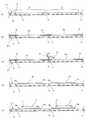
図1は第1の実施例の半導体装置の概略構成を示す平面図で、図2はその断面図である。[First embodiment]
FIG. 1 is a plan view showing a schematic configuration of the semiconductor device of the first embodiment, and FIG. 2 is a sectional view thereof.
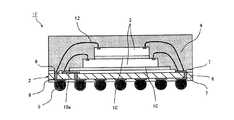
図1及び図2に示される本実施例の半導体装置1Aは、一面に所定の配線パターン(不図示)が形成された配線基板2と、この配線基板2の一面に搭載された半導体チップ3と、半導体チップ3の周囲を覆って半導体チップ3と配線基板2との電気接続部を封止する封止体4と、配線基板2の他面に配設された外部端子である半田ボール5等の金属ボールとを有する。尚、図1では封止体4を部分的に取り去って構造を分かりやすく示してある。 A semiconductor device 1A of the present embodiment shown in FIGS. 1 and 2 includes a
配線基板2は、基板面内にマトリックス状に区画された複数の製品形成部を有する略矩形のガラスエポキシ配線基板(以下、配線母基板と呼ぶ。)を製品形成部毎に分割して個片化したものである。配線基板2の絶縁基材6の一面と他面には所定の配線パターン(不図示)が形成されており、それらの配線は部分的に絶縁膜(例えばソルダーレジスト)7で覆われている。 The
配線基板2の一面に形成されている配線のうち、ソルダーレジストなどの絶縁膜7に覆われていない部分には、複数の接続パッド8が形成されている。また、配線基板2の他面に形成されている配線のうち、ソルダーレジストなどの絶縁膜7に覆われていない部分には、複数のランド9が形成されている。そして、接続パッド8とこれに対応するランド9とは、配線基板2の内部に形成された配線を介して電気的に接続されている。 A plurality of
半導体チップ3は、配線基板2の一面側の絶縁膜7上に接着部材10を介して搭載されている。接着部材10には、半導体チップ3の、電極パッド11を含む回路が形成されている一面(おもて面)とは反対側の面(裏面)が接着されている。電極パッド11とこれに対応する接続パッド8とは、導電性ワイヤ12によって電気的に接続されている。 The
接着部材10としては、例えば絶縁ペースト或いはDAF(Die Attached Film)等が用いられる。接着部材10は、その周端部10aが配線基板2の他面側の半田ボール5と重ならない位置、例えば格子状に配置された半田ボール5同士の間の位置に配置されるように設けられている。また接着部材10は、半導体チップ3の裏面サイズよりも大きいサイズで形成されており、接着部材10の周端部10aが半導体チップ3の周端部3aから張り出すように配置されている。 As the
このように本願は、接着部材10の周端部10aが半田ボール5と重ならない位置、例えば半田ボール5間の位置に配置されている半導体装置1Aを提供する。この構成により、接着部材10が塗布された領域と接着部材10の無い領域での弾性率の差により境界領域で発生する反りを、半田ボールと重なる領域では発生させないことが可能となる。また同時に、半導体装置1Aの温度変化による膨張収縮で半田ボール5に加わるせん断力も抑制される。したがって、二次実装の際に半田ボール5にかかる歪みを分散させることができ、半田ボール接続箇所での破断発生を低減し、半導体装置1Aの二次実装の信頼性を向上できる。 As described above, the present application provides the
また本願は、接着部材10の周端部10aが半導体チップ3の周端部3aより側方に張り出すように配置されている半導体装置1Aを提供している。このような構成では、半導体チップ3の周端部3aと接着部材10の周端部10aが異なる位置に配置されることで、半導体チップ3の周端部3aでの歪みと接着部材10の周端部10aでの歪みが一点に集中することなく、分散される為、二次実装の際に半田ボール5にかかる歪みをさらに低減することができる。 The present application also provides a
次に、半導体装置1Aの製造工程について説明する。 Next, the manufacturing process of the semiconductor device 1A will be described.
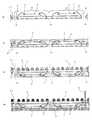
図3及び図4は、第1の実施例の半導体装置の組立フローを示す断面図である。 3 and 4 are sectional views showing an assembly flow of the semiconductor device of the first embodiment.
まず、図3(a)に示すような配線母基板2−1が準備される。配線母基板2−1は、基板面内にマトリックス状に区画された複数の製品形成部13(切断後に配線基板2となる部分)を有している。それぞれの製品形成部13間の境界には、製品形成部13毎に分割する際のダイシングライン14が設けられている。 First, a wiring mother board 2-1 as shown in FIG. The wiring mother board 2-1 has a plurality of product forming portions 13 (parts that become the
続いて、チップ接着部材10の配設工程が実施される。具体的には、配線母基板2−1の一面上に、図3(b)に示すように印刷用マスク15がセットされる。印刷用マスク15は、それぞれの製品形成部13に対応した複数の開口穴15aを有している。それぞれの開口穴15aは、その開口縁部が半田ボール搭載用のランド9の間の領域に配置されるように形成されている。尚、ランド9は配線母基板2−1の他面側に矩形の製品形成部13毎に格子状に配置されている。 Subsequently, an arrangement step of the
そして、図3(c)に示すように、印刷用マスク15上に塗布された接着部材10(例えば絶縁ペースト)をスキージ16で開口穴15a内に供給する。その後、印刷用マスク15を除去することで、図3(d)に示すように、それぞれの製品形成部13の一面に、所定の厚さの接着部材10の層を形成し、かつ、接着部材10の周端部10aをランド9の間に対応する位置に配置することができる。尚、接着部材10としては、絶縁ペーストに替えてDAF(Die Attached Film)を使用してもよい。 Then, as shown in FIG. 3C, the adhesive member 10 (for example, insulating paste) applied on the
次に、ダイボンディング工程が実施される。具体的には、図3(e)に示すように、配線母基板2−1のそれぞれの製品形成部13の一面に半導体チップ3が搭載される。接着部材10の層は、基板上を半導体チップ3が占めるサイズより大きいサイズで形成されている。これにより、接着部材10の周端部10aは半導体チップ3のそれぞれの辺から張り出すように配置されている。尚、接着部材10がDAFである場合、このように半導体チップ3が占めるサイズより大きく、かつ、基板上に貼り付けたときに周端部10aがランド9の間に対応する位置に配置できるDAFが使用される。 Next, a die bonding process is performed. Specifically, as shown in FIG. 3E, the
半導体チップ3は、その一面に論理回路、或いは記憶回路等が形成されたSi基板を有し、該Si基板の周辺近傍位置には複数の電極パッド11が形成されている。また、電極パッド11を除く半導体チップ3の一面には、回路形成面を保護するパッシベーション膜(不図示)が形成されている。第1の実施例においては、半導体チップ3の裏面側(回路形成面に対向する面)が接着部材10の層を介して配線母基板2−1の一面に接着固定される。 The
全ての製品形成部13に半導体チップ3を搭載し終えたらワイヤボンディング工程に移行する。図4(a)に示すように、ワイヤボンディング工程では、半導体チップ3の一面に形成されている電極パッド11と、それに対応する配線母基板2−1上の接続パッド8とが導電性のワイヤ12を介して接続される。かかるワイヤ12は例えばAu或いはCu等からなる。また、ワイヤボンディングには、図示しないワイヤボンディング装置が用いられる。具体的には、溶融され、ボールが形成されたワイヤ12の一端を、半導体チップ3の電極パッド11に超音波熱圧着した後、ワイヤ12の他端を配線母基板2−1上の対応する接続パッド8に超音波熱圧着する。尚、ワイヤ12は、半導体チップ3の端側の角との干渉を避けるために所定のループ形状を描くように形成される。 When the
続いて、配線母基板2−1は封止工程に移される。封止工程では、図4(b)に示すように、半導体チップ3が搭載された面側の複数の製品形成領域13を一括的に覆う封止体4が形成される。具体的には、上型と下型からなる成形金型(不図示)を有するトランスファモールド装置などの成型装置を用いて封止工程が実行される。上型には複数の製品形成部13を一括して覆う大きさのキャビティが形成されている。下型には配線母基板2−1を配置するための凹部が形成されている。ワイヤボンディング工程が完了した配線母基板2−1は、下型の凹部にセットされる。そして上型と下型で配線母基板2−1の周縁部をクランプすることで、配線母基板2−1の上方に、上記の大きさのキャビティが形成される。その後、熱硬化性の封止樹脂(例えばエポキシ樹脂)をキャビティの中へ充填し、所定の温度(例えば180℃)でキュアすることで、封止樹脂が硬化して封止体4が形成される。 Subsequently, the wiring mother board 2-1 is moved to a sealing process. In the sealing step, as shown in FIG. 4B, a sealing
次に、配線母基板2−1はボールマウント工程に移される。具体的には図4(c)に示すように、配線母基板2−1の他面の製品形成部13毎に格子状に配置された複数のランド9の上に、導電性の半田ボール5が接合される。ボールマウント工程では、配線母基板2−1上のランド9の配置に合わせて複数の吸着孔が形成された不図示のボールマウンターが用いられる。具体的には、半田ボール5が前記吸着孔に保持され、フラックスを介して、複数のランド9に一括的に接合される。 Next, the wiring mother board 2-1 is moved to a ball mounting process. Specifically, as shown in FIG. 4C,
その後、配線母基板2−1はダイシング工程に移される。具体的には、図4(d)に示すように、配線母基板2−1の封止体4側にダイシングテープ17が接着される。そして、ダイシング装置のダイシングブレード18により配線母基板2−1を縦横にダイシングライン14に沿って切断することで、各製品形成部13の間が分離される。その後、ダイシングテープ17から各製品形成部13をピックアップすることで、図1及び図2に示すような半導体装置1Aが得られる。 Thereafter, the wiring mother board 2-1 is moved to a dicing process. Specifically, as shown in FIG. 4D, the dicing
[第2の実施例]
次に、第2の実施例について説明するが、第1の実施例と同じ構成要素については同じ符号を用いることにする。図5は第2の実施例の半導体装置の概略構成を示す平面図、図6はその断面図である。[Second Embodiment]
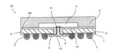
Next, the second embodiment will be described. The same reference numerals are used for the same components as those in the first embodiment. FIG. 5 is a plan view showing a schematic configuration of the semiconductor device of the second embodiment, and FIG. 6 is a sectional view thereof.
図5及び図6に示される本実施例の半導体装置1Bは、中央に開口部2aが形成された配線基板2と、この配線基板2の一面に搭載された半導体チップ3と、半導体チップ3の周囲を覆うと共に開口部2aにおける、半導体チップ3と配線基板2の電気接続部を封止する封止体4と、配線基板2の他面に配設された外部端子である半田ボール5の金属ボールとを有する。尚、図5では封止体4を部分的に取り去って構造を分かりやすく示してある。 A
配線基板2は、基板面内にマトリックス状に区画された複数の製品形成部を有する略矩形のガラスエポキシ配線基板(以下、配線母基板と呼ぶ。)を製品形成部毎に分割して個片化したものである。前記各製品形成部が相当する配線基板2の中央領域には、配線基板2の両面を貫通する細長い矩形の開口部2aが形成されている。また、配線基板2の絶縁基材6の他面には、開口部2aを除いて所定の配線パターン(不図示)が形成されている。それらの配線は部分的に絶縁膜(例えばソルダーレジスト)7で覆われている。 The
配線基板2の他面に形成されている配線のうち、ソルダーレジストなどの絶縁膜7に覆われていない部分には、複数の接続パッド8及びランド9が形成されている。そして、絶縁膜7に覆われている部分の配線は、接続パッド8とこれに対応するランド9とを電気的に接続する配線を含んでいる。 A plurality of
半導体チップ3は、配線基板2の一面上に接着部材10を介して搭載されている。接着部材10には、半導体チップ3の、電極パッド11を含む回路が形成されている一面(おもて面)が接着されている。複数の電極パッド11は半導体チップ3の中央領域に列状に配置され、配線基板2の開口部2aから露出している。また、複数の接続パッド8は、配線基板2の他面における開口部2aの2つの長辺の縁部に沿って配置されている。電極パッド11とこれに対応する接続パッド8とは、導電性ワイヤ12によって電気的に接続されている。これにより、半導体チップ3の電極パッド11とこれに対応するランド9とが電気的に接続される。 The
配線基板2は、細長い矩形の開口部2aにより分断された2つの領域、すなわち矩形の開口部2aの2つの長辺からその各長辺に対向する配線基板2の各端辺までの2つの領域を有する。そして、それぞれの領域の配線基板2の他面側(半導体チップ3と反対側の面)に複数のランド9が格子状に配置されている。それぞれのランド9には半田ボール5が接合されている。 The
配線基板2の一面側の接着部材10としては、例えば絶縁ペースト或いはDAF(Die Attached Film)等が用いられる。本実施例の接着部材10は、開口部2aにより分断されるそれぞれの領域に配置されている。それぞれの接着部材10は、矩形の開口部2aの1つの長辺からその長辺に対向する配線基板2の端辺に向かって拡がっている。そして、それぞれの接着部材10は、開口部2a側とは反対側の周端部10aが配線基板2の他面側の半田ボール5と重ならない位置、例えば格子状に配置された半田ボール5同士の間の位置に配置されるように設けられている。また接着部材10は、半導体チップ3の裏面サイズよりも大きいサイズで形成されている。これにより、接着部材10の周端部10aが半導体チップ3の周端部3aから張り出すように配置されている。 As the
このような位置に接着部材10の周端部10aを配置する効果は、第1の実施例で述べた効果と同じである。さらに本実施例は、半導体チップ3の回路形成面側を配線基板2の一面に接着するフェースダウン方式を採用したことで、配線基板2の一面側の封止体4の厚さを薄くできるため、半導体装置の薄型化を図ることができる。また、配線基板2の他面側に接続パッド8とランド9を形成することで、配線層が1層のみである配線基板を用いることができる。 The effect of disposing the
次に、半導体装置1Bの製造工程について説明する。 Next, the manufacturing process of the
図7及び図8は、第2の実施例の半導体装置の組立フローを示す断面図である。 7 and 8 are sectional views showing an assembly flow of the semiconductor device of the second embodiment.
まず、図7(a)に示すような配線母基板2−2が準備される。配線母基板2−2は、基板面内にマトリックス状に区画された複数の製品形成部13(切断後に配線基板2となる部分)を有している。それぞれの製品形成部13間の境界には、製品形成部13毎に分割する際のダイシングライン14が設けられている。さらに、各製品形成部13の中央には細長い矩形の開口部2aが形成されている。 First, a wiring mother board 2-2 as shown in FIG. 7A is prepared. The wiring mother board 2-2 has a plurality of product forming sections 13 (parts that become the
続いて、チップ接着部材10の配設工程が実施される。具体的には、配線母基板2−2の一面上に、図7(b)に示すように印刷用マスク15がセットされる。印刷用マスク15は、それぞれの製品形成部13に対応した複数の開口穴15aを有しており、それぞれの開口穴15aは、その開口縁部が半田ボール搭載用のランド9の間の領域に配置されるように形成されている。尚、ランド9は、配線母基板2−2の他面側であって製品形成部13毎の開口部2aの両側の領域に格子状に配置されている。 Subsequently, an arrangement step of the
そして、図7(c)に示すように、印刷用マスク15上に塗布された接着部材10(例えば絶縁ペースト)をスキージ16で開口穴15a内に供給する。その後、印刷用マスク15を除去することで、図7(d)に示すように、それぞれの製品形成部13の一面に、所定の厚さの接着部材10の層を形成し、かつ、接着部材10の、開口部2a側とは反対側の周端部10aをランド9の間に対応する位置に配置することができる。尚、接着部材10としては、絶縁ペーストに替えてDAF(Die Attached Film)を使用してもよい。 Then, as shown in FIG. 7C, the adhesive member 10 (for example, an insulating paste) applied on the
次に、ダイボンディング工程が実施される。具体的には、図7(e)に示すように、配線母基板2−2のそれぞれの製品形成部13の一面に半導体チップ3が搭載される。接着部材10の層は、基板上を半導体チップ3が占めるサイズより大きいサイズで形成されている。これにより、接着部材10の、開口部2a側とは反対側の周端部10aは半導体チップ3のそれぞれの辺から張り出すように配置されている。尚、接着部材10がDAFである場合、このように半導体チップ3が占めるサイズより大きく、かつ、基板上に貼り付けたときに周端部10aがランド9の間に対応する位置に配置できるDAFが使用される。 Next, a die bonding process is performed. Specifically, as shown in FIG. 7E, the
第2の実施例においては、半導体チップ3の回路形成面(電極パッド11が形成された面)を下向きにし、この回路形成面が、接着部材10の層を介して配線母基板2−2の一面に接着固定される。このとき、配線母基板2−2各製品形成部13の開口部2aから電極パッド11が露出するように半導体チップ3が固定される。 In the second embodiment, the circuit forming surface of the semiconductor chip 3 (the surface on which the
全ての製品形成部13に半導体チップ3を搭載し終えたらワイヤボンディング工程に移行する。図8(a)に示すように、ワイヤボンディング工程では、半導体チップ3の一面に形成されている電極パッド11と、それに対応する配線母基板2−2上の開口部2aの周辺近傍位置の接続パッド8とが導電性のワイヤ12を介して接続される。かかるワイヤ12は例えばAu或いはCu等からなる。また、ワイヤボンディングには、図示しないワイヤボンディング装置が用いられる。ワイヤ12は、開口部2aの周縁の角との干渉を避けるために所定のループ形状を描くように形成される。 When the
続いて、配線母基板2−2は封止工程に移される。封止工程では、図8(b)に示すように、半導体チップ3が搭載された面側の複数の製品形成領域13を一括的に覆う封止体4が形成される。この封止工程は、第1の実施形態と同様に、上型と下型からなる成形金型(不図示)を有するトランスファモールド装置などの成型装置を用いて実行される。下型には配線母基板2−2をセットするための凹部が形成されている。本実施例ではその凹部の基板支持面に、各製品形成部13の開口部2aへ熱硬化性の封止樹脂(例えばエポキシ樹脂)を注入可能な溝が形成されている。 Subsequently, the wiring motherboard 2-2 is moved to a sealing process. In the sealing step, as shown in FIG. 8B, a sealing
次に、配線母基板2−2はボールマウント工程に移される。具体的には図8(c)に示すように、配線母基板2−2の他面の製品形成部13毎に格子状に配置された複数のランド9の上に、導電性の半田ボール5が接合される。ボールマウント工程では、配線母基板2−2上のランド9の配置に合わせて複数の吸着孔が形成された不図示のボールマウンターが用いられ、半田ボール5が複数のランド4に一括的に接合される。 Next, the wiring mother board 2-2 is moved to a ball mounting process. Specifically, as shown in FIG. 8C,
その後、配線母基板2−2はダイシング工程に移される。具体的には、図8(d)に示すように、配線母基板2−2の封止体4側にダイシングテープ17が接着される。そして、ダイシング装置のダイシングブレード18により配線母基板2−2を縦横にダイシングライン14に沿って切断することで、各製品形成部13の間が分離される。その後、ダイシングテープ17から各製品形成部13をピックアップすることで、図5及び図6に示すような半導体装置1Bが得られる。 Thereafter, the wiring mother board 2-2 is moved to a dicing process. Specifically, as shown in FIG. 8D, the dicing
[第3の実施例]
次に、第3の実施例について説明するが、第1の実施例と同じ構成要素については同じ符号を用いることにする。図9は第3の実施例の半導体装置の概略構成を示す平面図、図10はその断面図である。[Third embodiment]
Next, a third embodiment will be described. The same reference numerals are used for the same components as those in the first embodiment. FIG. 9 is a plan view showing a schematic configuration of the semiconductor device of the third embodiment, and FIG. 10 is a sectional view thereof.
図9及び図10に示される本実施例の半導体装置1Cは、第2の実施例の半導体装置1Bとほぼ同様に構成されているが、接着部材10が配線基板2の一面側の略全面に形成されている点で異なる。具体的には、接着部材10の周端部10aが開口部2aの縁から配線基板2の外周端部2b近傍まで拡がっている。これにより、接着部材10の周端部10aが、格子状に配置された複数の半田ボール5からなる外部端子群の外側に配置されている。このように第3実施例では、接着部材10の周端部10aを半田ボール5と重ならない位置に配置することで、第1及び第2の実施例と同様の効果が得られる。すなわち、二次実装の際に半田ボール5にかかる歪みを低減することができる。 The
また第3の実施例では、接着部材10を配線基板2の一面の略全面に形成することで、接着部材10の周端部10aを半導体チップ3の周端部3aから第2の実施例よりも遠くに離間することができる。結果、半導体チップ3の周端部3aにおける歪みと接着部材10の周端部10aにおける歪みの干渉を第2の実施例よりも低減できる。 In the third embodiment, the
尚、接着部材10の周端部10aと配線基板2の外周端部2bが一致するように接着部材10を構成しても良い。しかし本実施例のように、接着部材10の周端部10aを配線基板2の周端部2aから僅かに内側に配置することで、半導体装置1Cの外側から接着部材10を通じて湿気が吸収されるのを抑制することができる。 Note that the
本実施例の半導体装置1Cの製造工程は第2の実施例の半導体装置1Bの製造工程と同じであるので、その説明は割愛する。 Since the manufacturing process of the
[第4の実施例]
次に、第4の実施例について説明するが、第1の実施例と同じ構成要素については同じ符号を用いることにする。図11は第4の実施例の半導体装置の概略構成を示す平面図である。図12の(a)は図11の半導体装置のコーナ部に対応する断面図、(b)はそのコーナ部以外の断面図である。[Fourth embodiment]
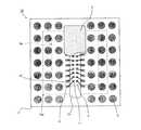
Next, a fourth embodiment will be described. The same reference numerals are used for the same components as those in the first embodiment. FIG. 11 is a plan view showing a schematic configuration of the semiconductor device of the fourth embodiment. 12A is a cross-sectional view corresponding to a corner portion of the semiconductor device of FIG. 11, and FIG. 12B is a cross-sectional view other than the corner portion.
図11及び図12に示される本実施例の半導体装置1Dは、第2の実施例の半導体装置1Bとほぼ同様に構成されているが、格子状に配置された半田ボール群が占める矩形状領域の4コーナに対応する、接着部材10の周端部10aの部位が、配線基板2の外周端部2bの近傍に配されている点で異なる。 The
第4実施例でも、接着部材10の周端部10aが半導体チップ3の周端部から張り出し、半田ボール5と重ならない位置に配置されており、第1及び第2の実施例と同様の効果が得られる。 Also in the fourth embodiment, the
特に本実施例では、半田ボール群が占める矩形状領域の4コーナに対応する、接着部材10の周端部10aの部位が、半田ボール群が占める領域の外側へ配線基板2の外周端部2bの近傍の位置まで拡げられている。これにより、半田ボール群が占める矩形状領域の4コーナにおける温度サイクル性を向上することができる。さらに、該4コーナに対応する部位以外の、接着部材10の周端部10aは、半田ボール群が占める領域の内側に位置し、半田ボール5の間の位置のような、半田ボール5と重ならない位置に配置されている。このため、配線基板2の外周端部2bから接着部材10を通じて湿気が吸収されるのを抑制することもできる。 In particular, in this embodiment, the
本実施例の半導体装置1Dの製造工程は第2の実施例の半導体装置1Bの製造工程と同じであるので、その説明は割愛する。 Since the manufacturing process of the
以上、本発明者によってなされた発明を実施例に基づき説明したが、本発明は上記実施例に限定されるものではなく、その要旨を逸脱しない範囲で種々変更可能であることは言うまでもない。例えば、上記の実施例では一つの配線基板に一つの半導体チップを搭載した半導体装置について説明したが、本発明はこれに限られない。図13に示すように配線基板2に最も近い半導体チップ3を配線基板2に接着する接着部材10の周端部10aを半田ボールと重ならない位置に配置した構成であれば、一つの配線基板2に複数の半導体チップ3が積層された半導体装置1Fも本願発明に含まれる。 As mentioned above, although the invention made | formed by this inventor was demonstrated based on the Example, this invention is not limited to the said Example, It cannot be overemphasized that it can change variously in the range which does not deviate from the summary. For example, in the above embodiment, the semiconductor device in which one semiconductor chip is mounted on one wiring board has been described, but the present invention is not limited to this. As shown in FIG. 13, if the configuration is such that the
尚、以下に付記する半導体装置もまた本願発明に含まれる。 The semiconductor device described below is also included in the present invention.
(付記1)配線基板と、
前記配線基板の一面に接着部材を介して搭載された半導体チップと、前記配線基板の他面に形成され、前記半導体チップと電気的に接続された外部電極とを有し、前記接着部材の周端部は前記外部電極と重ならない位置に配置されていることを特徴とする半導体装置。(Appendix 1) a wiring board;
A semiconductor chip mounted on one surface of the wiring substrate via an adhesive member; and an external electrode formed on the other surface of the wiring substrate and electrically connected to the semiconductor chip. The semiconductor device according to
(付記2)付記1に記載の半導体装置であって、前記接着部材の周端部が、前記半導体チップの周端部より外方に張り出すように配置されている半導体装置。 (Additional remark 2) It is a semiconductor device of
(付記3)付記1または2に記載の半導体装置であって、前記外部電極は導電性のボールであり、かつ前記配線基板の他面に格子状に配設されている半導体装置。 (Supplementary note 3) The semiconductor device according to
(付記4)付記3に記載の半導体装置であって、前記格子状に複数配設された導電性ボールの一群が占める領域のコーナに対応する、前記接着部材の周端部の部位が、前記配線基板の外周端部の近傍の位置に配されており、該コーナに対応する部位以外の、前記接着部材の周端部が前記領域の内側に位置し、前記導電性ボールの間の位置に配置されている半導体装置。 (Supplementary note 4) The semiconductor device according to
(付記5)付記1乃至4のいずれか1項に記載の半導体装置であって、前記半導体チップの、電極パッドを含む回路が形成された一面とは反対側の他面が前記配線基板の一面に接着されている半導体装置。 (Additional remark 5) It is a semiconductor device of any one of
(付記6)付記1乃至4のいずれか1項に記載の半導体装置であって、前記配線基板は前記配線基板の両面を貫通する開口部を有し、電極パッドを含む回路が形成された前記半導体チップの一面における該電極パッドが前記開口部から露出するように、該一面が前記配線基板の一面に接着されている半導体装置。 (Appendix 6) The semiconductor device according to any one of
(付記7)付記5に記載の半導体装置であって、前記配線基板の一面上の前記半導体チップの外方に形成され、前記半導体チップの前記電極パッドと電気的に接続される接続パッドを有し、前記接続パッドと前記外部電極が、前記配線基板の内部に形成された配線を介して導通されている半導体装置。 (Supplementary note 7) The semiconductor device according to
(付記8)付記6に記載の半導体装置であって、前記配線基板の他面における前記開口部の周縁近傍位置に形成され、前記開口部内に露出する前記半導体チップの前記電極パッドと電気的に接続される接続パッドを有し、前記接続パッドと前記外部電極が、前記配線基板の他面上に形成された配線を介して導通されている半導体装置。 (Additional remark 8) It is a semiconductor device of
(付記9)付記1乃至8のいずれか1項に記載の半導体装置であって、複数の前記半導体チップが前記配線基板の一面に対して垂直な方向に積層されている半導体装置。 (Supplementary note 9) The semiconductor device according to any one of
(付記10)付記1乃至8のいずれか1項に記載の半導体装置であって、前記接着部材が導電性ペーストからなる半導体装置。 (Appendix 10) The semiconductor device according to any one of
(付記11)付記1乃至10のいずれか1項に記載の半導体装置であって、前記配線基板の一面上に形成された、前記半導体チップの周囲を封止する封止体をさらに有する半導体装置。 (Appendix 11) The semiconductor device according to any one of
(付記12)付記1乃至11のいずれか1項に記載の半導体装置であって、前記電極パッドと前記接続パッドが導電性ワイヤを介して電気的に接続されている半導体装置。 (Supplementary note 12) The semiconductor device according to any one of
1A,1B,1C,1D,1F 半導体装置
2 配線基板
2a 開口部
2b 配線基板の外周端部
3 半導体チップ
3a 半導体チップの周端部
4 封止体
5 半田ボール
6 絶縁基材
7 絶縁膜
8 接続パッド
9 ランド
10 接着部材
10a 接着部材の周端部
11 電極パッド
12 導電性ワイヤ
13 製品形成部
14 ダイシングライン
15 印刷用マスク
15a 開口部
16 スキージ
17 ダイシングテープ
18 ダイシングブレード1A, 1B, 1C, 1D,
Claims (6)
Translated fromJapanese前記配線基板の一面に接着部材を介して搭載された半導体チップと、
前記配線基板の他面に形成され、前記半導体チップと電気的に接続された外部電極とを有し、
前記接着部材の周端部は前記外部電極と重ならない位置に配置されていることを特徴とする半導体装置。A wiring board;
A semiconductor chip mounted on one surface of the wiring board via an adhesive member;
An external electrode formed on the other surface of the wiring board and electrically connected to the semiconductor chip;
The semiconductor device according to claim 1, wherein a peripheral end portion of the adhesive member is disposed at a position not overlapping with the external electrode.
前記接着部材の周端部が、前記半導体チップの周端部より外方に張り出すように配置されている半導体装置。The semiconductor device according to claim 1,
The semiconductor device arrange | positioned so that the peripheral edge part of the said adhesive member may protrude outward from the peripheral edge part of the said semiconductor chip.
前記外部電極は導電性のボールであり、かつ前記配線基板の他面に格子状に配設されている半導体装置。The semiconductor device according to claim 1, wherein
The semiconductor device, wherein the external electrodes are conductive balls, and are arranged in a lattice pattern on the other surface of the wiring board.
前記格子状に配設された導電性ボールの一群が占める領域のコーナ部に対応する、前記接着部材の周端部の部位が、前記配線基板の外周端部の近傍の位置に配されており、該コーナ部に対応する部位以外の前記接着部材の周端部が前記領域の内側に位置し、前記導電性ボールの間の位置に配置されている半導体装置。The semiconductor device according to claim 3,
A portion of the peripheral end portion of the adhesive member corresponding to a corner portion of a region occupied by a group of conductive balls arranged in a lattice shape is disposed at a position near the outer peripheral end portion of the wiring board. A semiconductor device in which a peripheral end portion of the adhesive member other than a portion corresponding to the corner portion is located inside the region and disposed between the conductive balls.
前記半導体チップの、電極パッドを含む回路が形成された一面とは反対側の他面が前記配線基板の一面に接着されている半導体装置。5. The semiconductor device according to claim 1, wherein:
A semiconductor device in which the other surface of the semiconductor chip opposite to the surface on which a circuit including an electrode pad is formed is bonded to one surface of the wiring board.
前記配線基板は前記配線基板の両面を貫通する開口部を有し、
電極パッドを含む回路が形成された前記半導体チップの一面における該電極パッドが前記開口部から露出するように、該一面が前記配線基板の一面に接着されている半導体装置。5. The semiconductor device according to claim 1, wherein:
The wiring board has openings that penetrate both sides of the wiring board;
A semiconductor device in which the one surface is bonded to one surface of the wiring board so that the electrode pad on one surface of the semiconductor chip on which a circuit including the electrode pad is formed is exposed from the opening.
Priority Applications (3)
| Application Number | Priority Date | Filing Date | Title |
|---|---|---|---|
| JP2010280391AJP2012104790A (en) | 2010-10-12 | 2010-12-16 | Semiconductor device |
| US12/976,220US20120086111A1 (en) | 2010-10-12 | 2010-12-22 | Semiconductor device |
| US14/279,852US20140252613A1 (en) | 2010-10-12 | 2014-05-16 | Semiconductor device |
Applications Claiming Priority (3)
| Application Number | Priority Date | Filing Date | Title |
|---|---|---|---|
| JP2010229615 | 2010-10-12 | ||
| JP2010229615 | 2010-10-12 | ||
| JP2010280391AJP2012104790A (en) | 2010-10-12 | 2010-12-16 | Semiconductor device |
Publications (1)
| Publication Number | Publication Date |
|---|---|
| JP2012104790Atrue JP2012104790A (en) | 2012-05-31 |
Family
ID=45924490
Family Applications (1)
| Application Number | Title | Priority Date | Filing Date |
|---|---|---|---|
| JP2010280391ACeasedJP2012104790A (en) | 2010-10-12 | 2010-12-16 | Semiconductor device |
Country Status (2)
| Country | Link |
|---|---|
| US (2) | US20120086111A1 (en) |
| JP (1) | JP2012104790A (en) |
Families Citing this family (37)
| Publication number | Priority date | Publication date | Assignee | Title |
|---|---|---|---|---|
| KR101313391B1 (en) | 2004-11-03 | 2013-10-01 | 테세라, 인코포레이티드 | Stacked packaging improvements |
| US8058101B2 (en) | 2005-12-23 | 2011-11-15 | Tessera, Inc. | Microelectronic packages and methods therefor |
| US8482111B2 (en) | 2010-07-19 | 2013-07-09 | Tessera, Inc. | Stackable molded microelectronic packages |
| WO2012108469A1 (en)* | 2011-02-08 | 2012-08-16 | ローム株式会社 | Semiconductor device and semiconductor device manufacturing method |
| KR101128063B1 (en) | 2011-05-03 | 2012-04-23 | 테세라, 인코포레이티드 | Package-on-package assembly with wire bonds to encapsulation surface |
| US8836136B2 (en) | 2011-10-17 | 2014-09-16 | Invensas Corporation | Package-on-package assembly with wire bond vias |
| US8946757B2 (en) | 2012-02-17 | 2015-02-03 | Invensas Corporation | Heat spreading substrate with embedded interconnects |
| US8372741B1 (en) | 2012-02-24 | 2013-02-12 | Invensas Corporation | Method for package-on-package assembly with wire bonds to encapsulation surface |
| US8835228B2 (en) | 2012-05-22 | 2014-09-16 | Invensas Corporation | Substrate-less stackable package with wire-bond interconnect |
| US9391008B2 (en) | 2012-07-31 | 2016-07-12 | Invensas Corporation | Reconstituted wafer-level package DRAM |
| US9502390B2 (en) | 2012-08-03 | 2016-11-22 | Invensas Corporation | BVA interposer |
| US8878353B2 (en) | 2012-12-20 | 2014-11-04 | Invensas Corporation | Structure for microelectronic packaging with bond elements to encapsulation surface |
| US9136254B2 (en)* | 2013-02-01 | 2015-09-15 | Invensas Corporation | Microelectronic package having wire bond vias and stiffening layer |
| US8940630B2 (en) | 2013-02-01 | 2015-01-27 | Invensas Corporation | Method of making wire bond vias and microelectronic package having wire bond vias |
| JP2014165210A (en)* | 2013-02-21 | 2014-09-08 | Fujitsu Component Ltd | Module substrate |
| US9167710B2 (en) | 2013-08-07 | 2015-10-20 | Invensas Corporation | Embedded packaging with preformed vias |
| US9685365B2 (en) | 2013-08-08 | 2017-06-20 | Invensas Corporation | Method of forming a wire bond having a free end |
| US20150076714A1 (en) | 2013-09-16 | 2015-03-19 | Invensas Corporation | Microelectronic element with bond elements to encapsulation surface |
| US9583456B2 (en) | 2013-11-22 | 2017-02-28 | Invensas Corporation | Multiple bond via arrays of different wire heights on a same substrate |
| US9263394B2 (en) | 2013-11-22 | 2016-02-16 | Invensas Corporation | Multiple bond via arrays of different wire heights on a same substrate |
| US9583411B2 (en) | 2014-01-17 | 2017-02-28 | Invensas Corporation | Fine pitch BVA using reconstituted wafer with area array accessible for testing |
| US9406660B2 (en) | 2014-04-29 | 2016-08-02 | Micron Technology, Inc. | Stacked semiconductor die assemblies with die support members and associated systems and methods |
| US10381326B2 (en) | 2014-05-28 | 2019-08-13 | Invensas Corporation | Structure and method for integrated circuits packaging with increased density |
| US9735084B2 (en) | 2014-12-11 | 2017-08-15 | Invensas Corporation | Bond via array for thermal conductivity |
| US9888579B2 (en) | 2015-03-05 | 2018-02-06 | Invensas Corporation | Pressing of wire bond wire tips to provide bent-over tips |
| US9502372B1 (en) | 2015-04-30 | 2016-11-22 | Invensas Corporation | Wafer-level packaging using wire bond wires in place of a redistribution layer |
| US9761554B2 (en) | 2015-05-07 | 2017-09-12 | Invensas Corporation | Ball bonding metal wire bond wires to metal pads |
| US10490528B2 (en) | 2015-10-12 | 2019-11-26 | Invensas Corporation | Embedded wire bond wires |
| US9490222B1 (en) | 2015-10-12 | 2016-11-08 | Invensas Corporation | Wire bond wires for interference shielding |
| US10332854B2 (en) | 2015-10-23 | 2019-06-25 | Invensas Corporation | Anchoring structure of fine pitch bva |
| US10181457B2 (en) | 2015-10-26 | 2019-01-15 | Invensas Corporation | Microelectronic package for wafer-level chip scale packaging with fan-out |
| US10043779B2 (en) | 2015-11-17 | 2018-08-07 | Invensas Corporation | Packaged microelectronic device for a package-on-package device |
| US9659848B1 (en) | 2015-11-18 | 2017-05-23 | Invensas Corporation | Stiffened wires for offset BVA |
| US9984992B2 (en) | 2015-12-30 | 2018-05-29 | Invensas Corporation | Embedded wire bond wires for vertical integration with separate surface mount and wire bond mounting surfaces |
| US9935075B2 (en) | 2016-07-29 | 2018-04-03 | Invensas Corporation | Wire bonding method and apparatus for electromagnetic interference shielding |
| US10299368B2 (en) | 2016-12-21 | 2019-05-21 | Invensas Corporation | Surface integrated waveguides and circuit structures therefor |
| US20190206827A1 (en)* | 2017-12-29 | 2019-07-04 | Intel Corporation | Semiconductor package with externally accessible wirebonds |
Citations (2)
| Publication number | Priority date | Publication date | Assignee | Title |
|---|---|---|---|---|
| JP2002198458A (en)* | 2000-12-26 | 2002-07-12 | Nec Corp | Semiconductor device and its manufacturing method |
| JP2009212315A (en)* | 2008-03-04 | 2009-09-17 | Elpida Memory Inc | Semiconductor device and manufacturing method thereof |
Family Cites Families (7)
| Publication number | Priority date | Publication date | Assignee | Title |
|---|---|---|---|---|
| US5216278A (en)* | 1990-12-04 | 1993-06-01 | Motorola, Inc. | Semiconductor device having a pad array carrier package |
| US6157085A (en)* | 1998-04-07 | 2000-12-05 | Citizen Watch Co., Ltd. | Semiconductor device for preventing exfoliation from occurring between a semiconductor chip and a resin substrate |
| JP3437107B2 (en)* | 1999-01-27 | 2003-08-18 | シャープ株式会社 | Resin-sealed semiconductor device |
| US6242815B1 (en)* | 1999-12-07 | 2001-06-05 | Advanced Semiconductor Engineering, Inc. | Flexible substrate based ball grid array (BGA) package |
| EP1680811A2 (en)* | 2003-10-28 | 2006-07-19 | Dow Corning Corporation | Method for making a flat-top pad |
| US7422930B2 (en)* | 2004-03-02 | 2008-09-09 | Infineon Technologies Ag | Integrated circuit with re-route layer and stacked die assembly |
| US8564954B2 (en)* | 2010-06-15 | 2013-10-22 | Chipmos Technologies Inc. | Thermally enhanced electronic package |
- 2010
- 2010-12-16JPJP2010280391Apatent/JP2012104790A/ennot_activeCeased
- 2010-12-22USUS12/976,220patent/US20120086111A1/ennot_activeAbandoned
- 2014
- 2014-05-16USUS14/279,852patent/US20140252613A1/ennot_activeAbandoned
Patent Citations (2)
| Publication number | Priority date | Publication date | Assignee | Title |
|---|---|---|---|---|
| JP2002198458A (en)* | 2000-12-26 | 2002-07-12 | Nec Corp | Semiconductor device and its manufacturing method |
| JP2009212315A (en)* | 2008-03-04 | 2009-09-17 | Elpida Memory Inc | Semiconductor device and manufacturing method thereof |
Also Published As
| Publication number | Publication date |
|---|---|
| US20140252613A1 (en) | 2014-09-11 |
| US20120086111A1 (en) | 2012-04-12 |
Similar Documents
| Publication | Publication Date | Title |
|---|---|---|
| JP2012104790A (en) | Semiconductor device | |
| US8432033B2 (en) | Electronic device and manufacturing method therefor | |
| US8076770B2 (en) | Semiconductor device including a first land on the wiring substrate and a second land on the sealing portion | |
| JP5579402B2 (en) | Semiconductor device, method for manufacturing the same, and electronic device | |
| JP2015195263A (en) | Semiconductor device and manufacturing method or the same | |
| JP5543058B2 (en) | Manufacturing method of semiconductor device | |
| KR20020060558A (en) | Semiconductor device | |
| JP2009212315A (en) | Semiconductor device and manufacturing method thereof | |
| KR20070009428A (en) | Semiconductor device and manufacturing method therefor | |
| WO2014175133A1 (en) | Semiconductor device and method for manufacturing same | |
| KR20100069589A (en) | Semiconductor device | |
| JP2012230981A (en) | Semiconductor device and manufacturing method of the same | |
| US8098496B2 (en) | Wiring board for semiconductor device | |
| JP2010103348A (en) | Semiconductor device and method of manufacturing same | |
| JP2009147053A (en) | Semiconductor device and method of manufacturing the same | |
| US6410977B1 (en) | Semiconductor device, circuit board electronic instrument and method of making a semiconductor device | |
| JP5547703B2 (en) | Manufacturing method of semiconductor device | |
| JP2009283835A (en) | Semiconductor device and method of manufacturing the same | |
| JP2010010269A (en) | Semiconductor device, intermediate for manufacturing semiconductor device, and method of manufacturing them | |
| JP4942452B2 (en) | Circuit equipment | |
| JP2011061055A (en) | Method of manufacturing semiconductor device | |
| JP4038021B2 (en) | Manufacturing method of semiconductor device | |
| JP5666211B2 (en) | Wiring substrate and semiconductor device manufacturing method | |
| JP4737995B2 (en) | Semiconductor device | |
| JPH10154768A (en) | Semiconductor device and manufacturing method thereof |
Legal Events
| Date | Code | Title | Description |
|---|---|---|---|
| A711 | Notification of change in applicant | Free format text:JAPANESE INTERMEDIATE CODE: A711 Effective date:20130730 | |
| A621 | Written request for application examination | Free format text:JAPANESE INTERMEDIATE CODE: A621 Effective date:20131210 | |
| RD04 | Notification of resignation of power of attorney | Free format text:JAPANESE INTERMEDIATE CODE: A7424 Effective date:20140411 | |
| A977 | Report on retrieval | Free format text:JAPANESE INTERMEDIATE CODE: A971007 Effective date:20141023 | |
| A131 | Notification of reasons for refusal | Free format text:JAPANESE INTERMEDIATE CODE: A131 Effective date:20141028 | |
| A521 | Request for written amendment filed | Free format text:JAPANESE INTERMEDIATE CODE: A523 Effective date:20150128 | |
| RD03 | Notification of appointment of power of attorney | Free format text:JAPANESE INTERMEDIATE CODE: A7423 Effective date:20150327 | |
| RD04 | Notification of resignation of power of attorney | Free format text:JAPANESE INTERMEDIATE CODE: A7424 Effective date:20150403 | |
| A131 | Notification of reasons for refusal | Free format text:JAPANESE INTERMEDIATE CODE: A131 Effective date:20150707 | |
| A601 | Written request for extension of time | Free format text:JAPANESE INTERMEDIATE CODE: A601 Effective date:20150928 | |
| A521 | Request for written amendment filed | Free format text:JAPANESE INTERMEDIATE CODE: A523 Effective date:20160107 | |
| A01 | Written decision to grant a patent or to grant a registration (utility model) | Free format text:JAPANESE INTERMEDIATE CODE: A01 Effective date:20160126 | |
| A045 | Written measure of dismissal of application [lapsed due to lack of payment] | Free format text:JAPANESE INTERMEDIATE CODE: A045 Effective date:20160531 |