JP2012099825A - Substrate support having dynamic temperature control - Google Patents
Substrate support having dynamic temperature controlDownload PDFInfo
- Publication number
- JP2012099825A JP2012099825AJP2011259478AJP2011259478AJP2012099825AJP 2012099825 AJP2012099825 AJP 2012099825AJP 2011259478 AJP2011259478 AJP 2011259478AJP 2011259478 AJP2011259478 AJP 2011259478AJP 2012099825 AJP2012099825 AJP 2012099825A
- Authority
- JP
- Japan
- Prior art keywords
- heat transfer
- temperature
- transfer member
- substrate
- substrate support
- Prior art date
- Legal status (The legal status is an assumption and is not a legal conclusion. Google has not performed a legal analysis and makes no representation as to the accuracy of the status listed.)
- Pending
Links
- 239000000758substrateSubstances0.000titleclaimsabstractdescription159
- 238000012546transferMethods0.000claimsabstractdescription146
- 239000007788liquidSubstances0.000claimsabstractdescription83
- 238000012545processingMethods0.000claimsabstractdescription58
- 230000008859changeEffects0.000claimsabstractdescription13
- 239000000919ceramicSubstances0.000claimsdescription44
- 238000006243chemical reactionMethods0.000claimsdescription33
- 238000000034methodMethods0.000claimsdescription28
- 229910052751metalInorganic materials0.000claimsdescription15
- 239000002184metalSubstances0.000claimsdescription15
- 238000001816coolingMethods0.000claimsdescription10
- 238000004891communicationMethods0.000claimsdescription5
- 230000002093peripheral effectEffects0.000claimsdescription5
- 238000010438heat treatmentMethods0.000claimsdescription4
- 239000012530fluidSubstances0.000claimsdescription3
- 229920001971elastomerPolymers0.000claims4
- 239000000806elastomerSubstances0.000claims4
- 239000007789gasSubstances0.000description36
- 239000000463materialSubstances0.000description14
- 230000008569processEffects0.000description13
- 239000000853adhesiveSubstances0.000description7
- 230000001070adhesive effectEffects0.000description7
- 239000003989dielectric materialSubstances0.000description7
- 239000004065semiconductorSubstances0.000description7
- LYCAIKOWRPUZTN-UHFFFAOYSA-NEthylene glycolChemical compoundOCCOLYCAIKOWRPUZTN-UHFFFAOYSA-N0.000description6
- 238000005229chemical vapour depositionMethods0.000description5
- 238000005240physical vapour depositionMethods0.000description5
- 238000005530etchingMethods0.000description4
- 238000001020plasma etchingMethods0.000description4
- 229910052782aluminiumInorganic materials0.000description3
- XAGFODPZIPBFFR-UHFFFAOYSA-NaluminiumChemical compound[Al]XAGFODPZIPBFFR-UHFFFAOYSA-N0.000description3
- PNEYBMLMFCGWSK-UHFFFAOYSA-Naluminium oxideInorganic materials[O-2].[O-2].[O-2].[Al+3].[Al+3]PNEYBMLMFCGWSK-UHFFFAOYSA-N0.000description3
- 230000015572biosynthetic processEffects0.000description3
- 230000004044responseEffects0.000description3
- XLYOFNOQVPJJNP-UHFFFAOYSA-NwaterSubstancesOXLYOFNOQVPJJNP-UHFFFAOYSA-N0.000description3
- 229910000838Al alloyInorganic materials0.000description2
- 238000005266castingMethods0.000description2
- 229910010293ceramic materialInorganic materials0.000description2
- 238000009826distributionMethods0.000description2
- 239000013536elastomeric materialSubstances0.000description2
- 238000009616inductively coupled plasmaMethods0.000description2
- 238000002955isolationMethods0.000description2
- 238000003754machiningMethods0.000description2
- 239000007769metal materialSubstances0.000description2
- 239000000203mixtureSubstances0.000description2
- 229920002120photoresistant polymerPolymers0.000description2
- RYGMFSIKBFXOCR-UHFFFAOYSA-NCopperChemical compound[Cu]RYGMFSIKBFXOCR-UHFFFAOYSA-N0.000description1
- 229910000881Cu alloyInorganic materials0.000description1
- XUIMIQQOPSSXEZ-UHFFFAOYSA-NSiliconChemical compound[Si]XUIMIQQOPSSXEZ-UHFFFAOYSA-N0.000description1
- 230000005540biological transmissionEffects0.000description1
- 238000009529body temperature measurementMethods0.000description1
- 238000005219brazingMethods0.000description1
- 239000004020conductorSubstances0.000description1
- 238000010276constructionMethods0.000description1
- 229910052802copperInorganic materials0.000description1
- 239000010949copperSubstances0.000description1
- 230000008878couplingEffects0.000description1
- 238000010168coupling processMethods0.000description1
- 238000005859coupling reactionMethods0.000description1
- 230000003247decreasing effectEffects0.000description1
- 239000008367deionised waterSubstances0.000description1
- 229910021641deionized waterInorganic materials0.000description1
- 230000001419dependent effectEffects0.000description1
- 238000010891electric arcMethods0.000description1
- 230000005684electric fieldEffects0.000description1
- 238000005516engineering processMethods0.000description1
- 239000000945fillerSubstances0.000description1
- 239000001307heliumSubstances0.000description1
- 229910052734heliumInorganic materials0.000description1
- SWQJXJOGLNCZEY-UHFFFAOYSA-Nhelium atomChemical compound[He]SWQJXJOGLNCZEY-UHFFFAOYSA-N0.000description1
- 238000002513implantationMethods0.000description1
- 238000005468ion implantationMethods0.000description1
- 150000002500ionsChemical class0.000description1
- 238000004519manufacturing processMethods0.000description1
- 230000013011matingEffects0.000description1
- 229910001092metal group alloyInorganic materials0.000description1
- 238000003801millingMethods0.000description1
- 238000012986modificationMethods0.000description1
- 230000004048modificationEffects0.000description1
- 238000000465mouldingMethods0.000description1
- 239000003921oilSubstances0.000description1
- 239000002245particleSubstances0.000description1
- 239000010453quartzSubstances0.000description1
- 229910052710siliconInorganic materials0.000description1
- 239000010703siliconSubstances0.000description1
- VYPSYNLAJGMNEJ-UHFFFAOYSA-Nsilicon dioxideInorganic materialsO=[Si]=OVYPSYNLAJGMNEJ-UHFFFAOYSA-N0.000description1
- 230000008646thermal stressEffects0.000description1
- WFKWXMTUELFFGS-UHFFFAOYSA-NtungstenChemical compound[W]WFKWXMTUELFFGS-UHFFFAOYSA-N0.000description1
- 229910052721tungstenInorganic materials0.000description1
- 239000010937tungstenSubstances0.000description1
Images


Classifications
- F—MECHANICAL ENGINEERING; LIGHTING; HEATING; WEAPONS; BLASTING
- F27—FURNACES; KILNS; OVENS; RETORTS
- F27D—DETAILS OR ACCESSORIES OF FURNACES, KILNS, OVENS OR RETORTS, IN SO FAR AS THEY ARE OF KINDS OCCURRING IN MORE THAN ONE KIND OF FURNACE
- F27D5/00—Supports, screens or the like for the charge within the furnace
- F27D5/0037—Supports specially adapted for semi-conductors
- C—CHEMISTRY; METALLURGY
- C23—COATING METALLIC MATERIAL; COATING MATERIAL WITH METALLIC MATERIAL; CHEMICAL SURFACE TREATMENT; DIFFUSION TREATMENT OF METALLIC MATERIAL; COATING BY VACUUM EVAPORATION, BY SPUTTERING, BY ION IMPLANTATION OR BY CHEMICAL VAPOUR DEPOSITION, IN GENERAL; INHIBITING CORROSION OF METALLIC MATERIAL OR INCRUSTATION IN GENERAL
- C23C—COATING METALLIC MATERIAL; COATING MATERIAL WITH METALLIC MATERIAL; SURFACE TREATMENT OF METALLIC MATERIAL BY DIFFUSION INTO THE SURFACE, BY CHEMICAL CONVERSION OR SUBSTITUTION; COATING BY VACUUM EVAPORATION, BY SPUTTERING, BY ION IMPLANTATION OR BY CHEMICAL VAPOUR DEPOSITION, IN GENERAL
- C23C14/00—Coating by vacuum evaporation, by sputtering or by ion implantation of the coating forming material
- C23C14/22—Coating by vacuum evaporation, by sputtering or by ion implantation of the coating forming material characterised by the process of coating
- C23C14/50—Substrate holders
- C23C14/505—Substrate holders for rotation of the substrates
- C—CHEMISTRY; METALLURGY
- C23—COATING METALLIC MATERIAL; COATING MATERIAL WITH METALLIC MATERIAL; CHEMICAL SURFACE TREATMENT; DIFFUSION TREATMENT OF METALLIC MATERIAL; COATING BY VACUUM EVAPORATION, BY SPUTTERING, BY ION IMPLANTATION OR BY CHEMICAL VAPOUR DEPOSITION, IN GENERAL; INHIBITING CORROSION OF METALLIC MATERIAL OR INCRUSTATION IN GENERAL
- C23C—COATING METALLIC MATERIAL; COATING MATERIAL WITH METALLIC MATERIAL; SURFACE TREATMENT OF METALLIC MATERIAL BY DIFFUSION INTO THE SURFACE, BY CHEMICAL CONVERSION OR SUBSTITUTION; COATING BY VACUUM EVAPORATION, BY SPUTTERING, BY ION IMPLANTATION OR BY CHEMICAL VAPOUR DEPOSITION, IN GENERAL
- C23C16/00—Chemical coating by decomposition of gaseous compounds, without leaving reaction products of surface material in the coating, i.e. chemical vapour deposition [CVD] processes
- C23C16/44—Chemical coating by decomposition of gaseous compounds, without leaving reaction products of surface material in the coating, i.e. chemical vapour deposition [CVD] processes characterised by the method of coating
- C23C16/458—Chemical coating by decomposition of gaseous compounds, without leaving reaction products of surface material in the coating, i.e. chemical vapour deposition [CVD] processes characterised by the method of coating characterised by the method used for supporting substrates in the reaction chamber
- C23C16/4582—Rigid and flat substrates, e.g. plates or discs
- C23C16/4583—Rigid and flat substrates, e.g. plates or discs the substrate being supported substantially horizontally
- C23C16/4586—Elements in the interior of the support, e.g. electrodes, heating or cooling devices
- C—CHEMISTRY; METALLURGY
- C23—COATING METALLIC MATERIAL; COATING MATERIAL WITH METALLIC MATERIAL; CHEMICAL SURFACE TREATMENT; DIFFUSION TREATMENT OF METALLIC MATERIAL; COATING BY VACUUM EVAPORATION, BY SPUTTERING, BY ION IMPLANTATION OR BY CHEMICAL VAPOUR DEPOSITION, IN GENERAL; INHIBITING CORROSION OF METALLIC MATERIAL OR INCRUSTATION IN GENERAL
- C23C—COATING METALLIC MATERIAL; COATING MATERIAL WITH METALLIC MATERIAL; SURFACE TREATMENT OF METALLIC MATERIAL BY DIFFUSION INTO THE SURFACE, BY CHEMICAL CONVERSION OR SUBSTITUTION; COATING BY VACUUM EVAPORATION, BY SPUTTERING, BY ION IMPLANTATION OR BY CHEMICAL VAPOUR DEPOSITION, IN GENERAL
- C23C16/00—Chemical coating by decomposition of gaseous compounds, without leaving reaction products of surface material in the coating, i.e. chemical vapour deposition [CVD] processes
- C23C16/44—Chemical coating by decomposition of gaseous compounds, without leaving reaction products of surface material in the coating, i.e. chemical vapour deposition [CVD] processes characterised by the method of coating
- C23C16/46—Chemical coating by decomposition of gaseous compounds, without leaving reaction products of surface material in the coating, i.e. chemical vapour deposition [CVD] processes characterised by the method of coating characterised by the method used for heating the substrate
- C23C16/463—Cooling of the substrate
- C23C16/466—Cooling of the substrate using thermal contact gas
- H—ELECTRICITY
- H01—ELECTRIC ELEMENTS
- H01J—ELECTRIC DISCHARGE TUBES OR DISCHARGE LAMPS
- H01J37/00—Discharge tubes with provision for introducing objects or material to be exposed to the discharge, e.g. for the purpose of examination or processing thereof
- H01J37/32—Gas-filled discharge tubes
- H01J37/32009—Arrangements for generation of plasma specially adapted for examination or treatment of objects, e.g. plasma sources
- H01J37/32082—Radio frequency generated discharge
- H01J37/321—Radio frequency generated discharge the radio frequency energy being inductively coupled to the plasma
- H—ELECTRICITY
- H01—ELECTRIC ELEMENTS
- H01L—SEMICONDUCTOR DEVICES NOT COVERED BY CLASS H10
- H01L21/00—Processes or apparatus adapted for the manufacture or treatment of semiconductor or solid state devices or of parts thereof
- H01L21/67—Apparatus specially adapted for handling semiconductor or electric solid state devices during manufacture or treatment thereof; Apparatus specially adapted for handling wafers during manufacture or treatment of semiconductor or electric solid state devices or components ; Apparatus not specifically provided for elsewhere
- H01L21/67005—Apparatus not specifically provided for elsewhere
- H01L21/67011—Apparatus for manufacture or treatment
- H01L21/67098—Apparatus for thermal treatment
- H01L21/67109—Apparatus for thermal treatment mainly by convection
- H—ELECTRICITY
- H01—ELECTRIC ELEMENTS
- H01L—SEMICONDUCTOR DEVICES NOT COVERED BY CLASS H10
- H01L21/00—Processes or apparatus adapted for the manufacture or treatment of semiconductor or solid state devices or of parts thereof
- H01L21/67—Apparatus specially adapted for handling semiconductor or electric solid state devices during manufacture or treatment thereof; Apparatus specially adapted for handling wafers during manufacture or treatment of semiconductor or electric solid state devices or components ; Apparatus not specifically provided for elsewhere
- H01L21/683—Apparatus specially adapted for handling semiconductor or electric solid state devices during manufacture or treatment thereof; Apparatus specially adapted for handling wafers during manufacture or treatment of semiconductor or electric solid state devices or components ; Apparatus not specifically provided for elsewhere for supporting or gripping
- H01L21/6831—Apparatus specially adapted for handling semiconductor or electric solid state devices during manufacture or treatment thereof; Apparatus specially adapted for handling wafers during manufacture or treatment of semiconductor or electric solid state devices or components ; Apparatus not specifically provided for elsewhere for supporting or gripping using electrostatic chucks
- H—ELECTRICITY
- H01—ELECTRIC ELEMENTS
- H01J—ELECTRIC DISCHARGE TUBES OR DISCHARGE LAMPS
- H01J2237/00—Discharge tubes exposing object to beam, e.g. for analysis treatment, etching, imaging
- H01J2237/20—Positioning, supporting, modifying or maintaining the physical state of objects being observed or treated
- H01J2237/2001—Maintaining constant desired temperature
Landscapes
- Chemical & Material Sciences (AREA)
- Engineering & Computer Science (AREA)
- Mechanical Engineering (AREA)
- Physics & Mathematics (AREA)
- Organic Chemistry (AREA)
- Chemical Kinetics & Catalysis (AREA)
- Materials Engineering (AREA)
- Metallurgy (AREA)
- General Chemical & Material Sciences (AREA)
- Condensed Matter Physics & Semiconductors (AREA)
- Microelectronics & Electronic Packaging (AREA)
- Power Engineering (AREA)
- Manufacturing & Machinery (AREA)
- Computer Hardware Design (AREA)
- General Physics & Mathematics (AREA)
- General Engineering & Computer Science (AREA)
- Plasma & Fusion (AREA)
- Analytical Chemistry (AREA)
- Drying Of Semiconductors (AREA)
- Container, Conveyance, Adherence, Positioning, Of Wafer (AREA)
- Chemical Vapour Deposition (AREA)
Abstract
Description
Translated fromJapanese発明の背景
プラズマ処理装置は、例えば、半導体材料、誘電体材料及び金属材料のプラズマ・エッチング、物理気相成長、 化学気相成長(“CVD”)、物理気相成長(“PVD”)、イオン注入及びレジスト剥離のために使用される。BACKGROUND OF THE INVENTION Plasma processing equipment includes, for example, plasma etching, physical vapor deposition, chemical vapor deposition (“CVD”), physical vapor deposition (“PVD”), ions of semiconductor materials, dielectric materials and metal materials. Used for implantation and resist stripping.
半導体材料処理で使用されるプラズマ処理装置の1つのタイプは、反応チャンバを含む。処理基板は、基板支持体上で反応チャンバ内に支持される。基板は、典型的には、基板ホルダによって基板支持体上に固定される。処理ガスは、ガス分配システムによって反応チャンバ内に導入される。電界は、基板を処理する処理ガスからプラズマを生成するように形成される。 One type of plasma processing apparatus used in semiconductor material processing includes a reaction chamber. The processing substrate is supported in the reaction chamber on the substrate support. The substrate is typically secured on a substrate support by a substrate holder. Process gas is introduced into the reaction chamber by a gas distribution system. The electric field is formed to generate plasma from a processing gas that processes the substrate.
発明の概要
基板支持体が提供される。基板支持体は、基板を処理している間に基板がその上に支持される支持体の表面で、動的な温度制御を提供することができる。基板支持体は、例えば、プラズマ処理装置の反応室をプラズマエッチングするのに役に立つ。SUMMARY OF THE INVENTION A substrate support is provided. The substrate support can provide dynamic temperature control at the surface of the support on which the substrate is supported while processing the substrate. The substrate support is useful, for example, for plasma etching a reaction chamber of a plasma processing apparatus.
基板支持体の好適な実施形態は、セラミック部材、セラミック部材の上に位置する金属熱伝達部材及び熱伝達部材の上に位置する静電チャックを備える。熱伝達部材は、小さい熱質量(low thermal mass)を有する。熱伝達部材は、少なくとも1つの流路を含み、それを通して熱伝達部材を加熱する及び/又は冷却するために、液体が循環することができる。静電チャックは、静電気的に基板をクランプすることができる支持体の表面を有する。基板支持体は、好適には、1つ以上の流路と温度制御された流れの伝達がある液体源を備える。基板支持体はまた、好適には、支持体の表面と基板との間に熱伝達ガスを供給するために動作可能な熱伝達ガス源を備える。随意的なコントローラは、液体の制御パラメータ及び基板支持体に供給される熱伝達ガスを制御するように、液体源及び熱伝達ガス源の制御動作を制御することができる。 A preferred embodiment of the substrate support comprises a ceramic member, a metal heat transfer member located on the ceramic member, and an electrostatic chuck located on the heat transfer member. The heat transfer member has a low thermal mass. The heat transfer member includes at least one flow path through which the liquid can circulate to heat and / or cool the heat transfer member. An electrostatic chuck has a support surface that can electrostatically clamp a substrate. The substrate support preferably comprises a liquid source with one or more flow paths and temperature controlled flow transmission. The substrate support also preferably comprises a heat transfer gas source operable to supply a heat transfer gas between the surface of the support and the substrate. An optional controller can control the liquid source and heat transfer gas source control operations to control the liquid control parameters and the heat transfer gas supplied to the substrate support.
熱伝達部材は、好適には、1つ以上の流路に供給される液体によって急速に加熱及び/又は冷却されうる。従って、基板支持体は、基板支持体上で基板の動的な熱制御を提供することができる。 The heat transfer member can preferably be rapidly heated and / or cooled by liquid supplied to one or more flow paths. Thus, the substrate support can provide dynamic thermal control of the substrate on the substrate support.
プラズマ処理装置内で基板を処理する方法の好適な実施形態は、プラズマ処理装置の反応チャンバ内の静電チャックの支持表面の上に基板を支持する工程と、基板の温度を制御するために静電チャックの下に位置する金属熱伝達部材内の少なくとも1つの通路を通して液体を循環させる工程と、を含む。熱伝達部材は、小さい熱質量(low thermal mass)を有する。 A preferred embodiment of a method for processing a substrate in a plasma processing apparatus includes supporting a substrate on a support surface of an electrostatic chuck in a reaction chamber of the plasma processing apparatus, and statically controlling the substrate temperature. Circulating a liquid through at least one passage in a metal heat transfer member located under the electric chuck. The heat transfer member has a low thermal mass.
基板(例えば、半導体ウェハ、フラットパネルディスプレイ基板、誘電体材料等)のプラズマ処理の間、処理基板から作製されたデバイスが十分な電気特性を持つように、出来るだけ均一に、材料がエッチングによって基板から取り除かれるか、又は材料が基板上に成膜されることが好ましい。しかしながら、基板上に形成されたフィーチャ(feature)のサイズが減少する一方で、基板サイズが増大するにつれて、この目標を達成するのが益々困難となっている。 During plasma processing of a substrate (eg, semiconductor wafer, flat panel display substrate, dielectric material, etc.), the material is etched by the substrate as uniformly as possible so that devices made from the processed substrate have sufficient electrical properties. Or is preferably deposited on the substrate. However, while the size of features formed on the substrate has decreased, it has become increasingly difficult to achieve this goal as the substrate size increases.
プラズマ処理装置内の基板のプラズマ処理の均一性を向上させるために、エッチングが行われ、その上に(例えば、CVD又はPVD技術によって)材料が成膜され、及び/又はフォトレジストが剥離される、基板の露出した表面における温度を制御することが好ましい。プラズマ・エッチングでは、基板温度の変動及び/又は基板の露出した表面での化学反応の速度における変動によって、エッチング選択性及び異方性における変動に加えて、基板のエッチング速度の変動を引き起こしうる。例えば、ウェハの温度がある温度よりも上昇すると、ウェハダメージ(例えば、フォトレジストダメージ)が生じ、温度に依存する化学反応が変化しうる。材料成膜処理では、基板上に成膜される材料の構成と特性に加えて、成膜中の基板温度の変化によって、成膜速度が大きく変化しうる。 In order to improve the uniformity of the plasma processing of the substrate in the plasma processing apparatus, etching is performed, a material is deposited thereon (for example, by CVD or PVD technology), and / or the photoresist is stripped. It is preferable to control the temperature at the exposed surface of the substrate. In plasma etching, variations in substrate temperature and / or variations in the rate of chemical reactions at the exposed surface of the substrate can cause variations in the etch rate of the substrate in addition to variations in etch selectivity and anisotropy. For example, when the temperature of the wafer rises above a certain temperature, wafer damage (eg, photoresist damage) can occur, and the temperature-dependent chemical reaction can change. In the material film formation process, in addition to the configuration and characteristics of the material to be formed on the substrate, the film formation rate can be greatly changed by the change in the substrate temperature during film formation.
基板支持体と基板支持体上に支持される基板との間の熱伝達を向上させるために、基板支持体は、裏面ガス冷却システムを含むことができる。しかしながら、熱伝達ガスの熱伝達能力は、基板支持体の表面条件に依存する。表面条件が処理の間に変化するにつれて、基板から熱を取り除く熱伝達ガスの能力も変化しうる。 In order to improve heat transfer between the substrate support and the substrate supported on the substrate support, the substrate support can include a backside gas cooling system. However, the heat transfer capability of the heat transfer gas depends on the surface conditions of the substrate support. As surface conditions change during processing, the ability of the heat transfer gas to remove heat from the substrate can also change.
基板支持体は、処理の間に熱を取り除く液体冷却システムを含むことができる。このようなシステムでは、基板支持体の金属本体(「冷却板」)内の1つ以上の流路を通って液体が流れるか又は金属本体を冷却し、それによって基板支持体上の基板の温度を変化させる。本体が加熱又は冷却されうる速度は、本体の熱容量(heat capacity)又は‘‘熱質量(thermal mass)’’Cに関係する。本体の熱質量は、本体の材料の比熱容量(specific heat capacity)c、及び本体の質量mの積に等しい(すなわち、C=c・m)。従って、本体の熱質量は、その質量を変化させることによって変化することができ、これは本体の体積を変化させることによって実現することができる。また、本体の温度をΔTだけ変化させるために、本体を加熱することによって本体に与えられる必要がある熱量q又は本体を冷却することによって本体により放出される必要がある熱量qは、q=c・m・ΔTで与えられる。その結果、本体の熱質量が増加するにつれて、本体の温度をΔTだけ変化させるために、本体に与えられる必要がある熱量又は本体から取り除く必要がある熱量も増大する。 The substrate support can include a liquid cooling system that removes heat during processing. In such a system, liquid flows or cools the metal body through one or more channels in the metal body ("cooling plate") of the substrate support, thereby causing the temperature of the substrate on the substrate support. To change. The rate at which the body can be heated or cooled is related to the heat capacity or 'thermal mass' C of the body. The thermal mass of the body is equal to the product of the specific heat capacity c of the body material and the mass m of the body (ie C = c · m). Thus, the thermal mass of the body can be changed by changing its mass, which can be achieved by changing the volume of the body. Further, in order to change the temperature of the main body by ΔT, the amount of heat q that needs to be given to the main body by heating the main body or the amount of heat q that needs to be released by the main body by cooling the main body is q = c • It is given by m · ΔT. As a result, as the thermal mass of the body increases, so does the amount of heat that needs to be applied to or removed from the body in order to change the temperature of the body by ΔT.
大きい熱質量(例えば、11/4インチ以上の厚さを有する金属冷却板)を持つ冷却板を含む基板支持体、そしてまた大きい液体容量を有する液体供給部は、プラズマ処理の間、固定された温度に基板支持体を維持するために、液体を冷却板内の流路に供給することができる。しかしながら、基板支持体の温度を素早く変化させる液体によって、多量の熱が基板支持体に加えられるか又は基板支持体から取り除かれなければならないので、そのような基板支持体が動的な温度制御能力を有しないことが分かった。その結果、そのような大きな熱質量を有する基板支持体は、基板支持体上に支持される基板の応答性の良い温度制御を提供しない。 A substrate support including a cold plate with a large thermal mass (eg, a metal cold plate having a thickness of 11/4 inches or more), and also a liquid supply with a large liquid capacity, was fixed during plasma processing. In order to maintain the substrate support at temperature, liquid can be supplied to the channels in the cooling plate. However, liquids that rapidly change the temperature of the substrate support require that a large amount of heat be applied to or removed from the substrate support so that such substrate support has a dynamic temperature control capability. Was found to have no As a result, a substrate support having such a large thermal mass does not provide responsive temperature control of a substrate supported on the substrate support.
熱伝達部材を所望の温度に急速に加熱する及び/又は冷却することが可能な、小さな熱質量を持つ熱伝達部材を使用することによって、動的な温度制御能力を有する基板支持体を提供することができることが分かった。 Providing a substrate support with dynamic temperature control capability by using a heat transfer member with a small thermal mass capable of rapidly heating and / or cooling the heat transfer member to a desired temperature I found out that I could do it.
好適な実施形態では、基板支持体は、液体を供給して必要な温度に熱伝達部材を加熱する及び/又は冷却するために動作可能な液体源を備える。熱伝達部材は、少なくとも1つの流路を含み、それを通して熱伝達部材に又は熱伝達部材からの熱伝達の速度を向上させる液体源から液体が循環される。液体源は、好適には、少量の液体を加熱及び/又は冷却することができる。温度制御された液体が熱伝達部材に供給され、素早い応答能力を与えることができる。基板支持体の表面の動的な温度制御は、小さい熱質量を有する熱伝達部材及び素早い応答能力を有する液体源の組み合わせによって、向上させることができる。液体源はまた、好適には、その温度及び/又は流量などの選択された液体のパラメータを制御することができる。 In a preferred embodiment, the substrate support comprises a liquid source operable to supply liquid and heat and / or cool the heat transfer member to the required temperature. The heat transfer member includes at least one flow path through which liquid is circulated from a liquid source that increases the rate of heat transfer to or from the heat transfer member. The liquid source can suitably heat and / or cool a small amount of liquid. A temperature-controlled liquid can be supplied to the heat transfer member to provide a quick response capability. Dynamic temperature control of the surface of the substrate support can be improved by a combination of a heat transfer member having a small thermal mass and a liquid source having a quick response capability. The liquid source can also preferably control selected liquid parameters such as its temperature and / or flow rate.
好適な実施形態では、基板支持体は、熱伝達ガスを基板支持体の上面と基板との間に供給するために動作可能である熱伝達ガス源を含む。 In a preferred embodiment, the substrate support includes a heat transfer gas source that is operable to supply heat transfer gas between the top surface of the substrate support and the substrate.
好適な実施形態に係る基板支持体がその内部で使用可能である例示的なプラズマ反応室は図1に示される。プラズマ反応室は、誘導結合プラズマ反応室である。また、プラズマ処理の間に基板の温度制御が必要な他のタイプのプラズマ反応室内で基板支持体が使用されうる。例えば、基板支持体は、他の誘導結合プラズマ反応室構造、電子サイクロトロン共鳴(“ECR”)、マグネトロン及び容量結合プラズマ反応室内で使用されうる。 An exemplary plasma reaction chamber in which a substrate support according to a preferred embodiment can be used is shown in FIG. The plasma reaction chamber is an inductively coupled plasma reaction chamber. Also, the substrate support can be used in other types of plasma reaction chambers that require temperature control of the substrate during plasma processing. For example, the substrate support can be used in other inductively coupled plasma reaction chamber structures, electron cyclotron resonance (“ECR”), magnetron and capacitively coupled plasma reaction chambers.
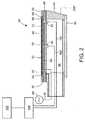
図1に示されるプラズマ反応室は、静電チャック34を有する基板支持体12を含む反応チャンバ10を備える。静電チャック34は、基板13を静電気的にクランプするほかに基板にRFバイアスを与える。例えば、基板13は、半導体ウェハであってもよい。フォーカスリング14は、基板13の上方のプラズマを増加させる。エネルギ源は、反応チャンバ10の上部に配置され、処理ガスにエネルギを与えて、反応チャンバ内にプラズマを生成する。エネルギ源は、例えば、RF源19によってパワーが与えられるアンテナ18であってもよい。反応チャンバ10は、所望の圧力にチャンバの内部を維持するための真空ポンプ装置を含む。 The plasma reaction chamber shown in FIG. 1 includes a
誘電体窓20は、アンテナ18と処理チャンバ10の内部との間に配置される。ガス分配板22は、ウィンドウ20の下にあって、それを通して処理ガスがガス供給部23から反応チャンバ10まで供給される開口部を含む。 The
動作中は、基板13は、基板ホルダ12の露出した上面に配置され、静電チャック34によって静電気的にクランプされる。熱伝達ガスは、好適には、基板13とその上面との間の熱伝達を向上させるために、基板ホルダ12の上面と基板13との間に導入される。処理ガスは、反応チャンバ10に供給される。プラズマは、反応チャンバ10内でRFパワーをアンテナ18に供給することによって生成される。 During operation, the
図2は、基板支持体40の好適な実施形態を示す図である。例えば、反応チャンバ10内で基板支持体40を使用することができる。基板支持体40は、下部カバー42、カバー42上のベース44、ベース44の上に配置され、内部空間56を囲むセラミック部材46、セラミック部材46の上に位置する低熱質量伝達部材(low-mass heat transfer member)48、及び、熱伝達部材48の上に位置する静電チャック50を備える。RF電源49は、RFバイアスを提供するために、導電体51を通して電気的に熱伝達部材48に接続される。エッジリング52は、セラミック部材46の上に配置されて、熱伝達部材48及び静電チャック50を取り囲む。エッジリング52は、石英(quartz)やSiCなどで作られうる。基板70は、静電チャック50の上に支持された状態で示される。 FIG. 2 is a view showing a preferred embodiment of the
基板支持体40は、熱伝達部材48内に提供される1つ以上の流路と流れの伝達がある入口58と出口60を含む。入口58及びと出口60は、供給ライン102と戻りライン104をそれぞれ通って液体源100と流れの伝達がある。液体は、液体源100から供給ライン102を介して、熱伝達部材48の流路内に入口58を介して循環し、この流路を通って液体源100に出口60及び戻りライン104を介して戻る。液体源100の動作は、好適には、液体源100と流れの伝達があるコントローラ200によって制御される。 The
ベース44は、アルミニウム、アルミ合金などの金属で作られる。ベース44は電気的に接地される。 The
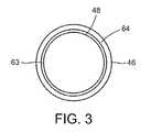
図2に示される実施形態では、セラミック部材46は、ベース44に固定される。例えば、ベース44にセラミック部材46を固定するボルト、ねじなどの接合留め具(mating fastener)を受けるために、金属挿入物などをセラミック部材46に挿入することができる。セラミック部材46は適当な材料で作られ、また、セラミック部材46の下部表面62の上に作用する圧力(典型的には大気圧)を相殺するのに十分な剛性を持つように構成される。セラミック部材46は、好適には、プラズマ処理の間のゆがみ(deflection)に耐えるのに十分に高い係数(例えば、少なくとも15Mpsi)を有する。セラミック部材46のゆがみを最小化することによって、プラズマ処理の間、セラミック部材46並びにその上に位置する熱伝達部材48及び静電チャック50の寸法安定性(dimensional stability)が維持される。例えば、セラミック部材46は、最も薄い部分で約1〜4mmの厚さを持つことができる。処理の間、ベース44は、熱伝達部材48よりも更に高いか又は更に低い温度のいずれかであってもよい。セラミック部材46は、好適には、ベース44から熱的に絶縁するのに十分に低い熱伝導率を有する。さらに、セラミック部材46は、接地(ground)からRF駆動される熱伝達部材48に対しRF絶縁(RFisolation)を提供する。セラミック部材46は、アルミナ(A1203)などの他の適当な材料で作ることができる。 In the embodiment shown in FIG. 2, the
好適な実施形態では、セラミック部材46の上部は、周辺フランジ64によって取り囲まれた、中央が凹んだ表面63を有する。凹んだ表面63は、セラミック部材46が作られた後に、フライス削り(milling)などの機械加工処理によって形成することができる。また、凹んだ表面63は、例えば、モールド(molding)又はキャスティング(casting)によって、セラミック部材46を形成するために使用される処理によって形成することができる。熱伝達部材48は、凹んだ表面63、好適にはフランジ64と同一平面上に配置される。 In the preferred embodiment, the top of the
熱伝達部材48は、好適には、セラミック部材46の凹んだ表面63に接着して結合される。セラミック部材46と熱伝達部材48との間に与えられる接着剤は、好適には、セラミック部材46から熱伝達部材48を熱的に絶縁する低い熱伝導率を有する。接着剤はまた、好適には、半導体基板のプラズマ処理の間に、セラミック部材46と熱伝達部材48との間に生じる熱ストレスを緩和する(accommodate)のに十分な弾性を有する。接着剤は、好適には、ゼネラル・エレクトリック社からRTV 133とRTV 167として入手可能な室温硬化接着剤(room temperature-curing adhesive)などのエラストマー材料である。 The
熱伝達部材48は、熱伝達部材48の周辺エッジがフランジ64から横方向に間隔が空くように、凹んだ表面63の幅よりも小さな幅を持つことが好ましい。例えば、凹んだ表面63は円形であり、また、熱伝達部材48は円形かつ凹んだ表面よりも小さい直径を持つすることができる(図3)。静電チャック50は、フランジ64及び熱伝達部材48の上に搭載される。例えば、300mmウェハを処理する場合には、静電チャック50は、静電チャック50がフランジ64に接触するように、例えば、約298mmなどの凹んだ表面63及びウェハの直径にほぼ等しい直径を持つことができる。熱伝達部材48は、約298mm未満の直径を持つことができるので、フランジ64から間隔が空いている。 The
図4では、熱伝達部材48は、好適には、ベース72及び上に位置するカバー74を含む。熱伝達部材48は、銅、銅の合金、アルミニウム、アルミ合金などの十分な熱伝達特性を持つ金属で作られうる。ベース72及びカバー74は、好適には、ろう付けなどによって接合され、その間に流体シールを提供する。 In FIG. 4, the
ベース72は、好適には、約1/4インチ以下、より好適には約1/8インチ以下の厚さを有する。カバー74は、好適には、約1/16インチ以下の厚さを有する。ベース72及びカバー74は、好適には、約1/4インチ、より好適には約1/8インチの最大結合厚さ(maximum combined thickness)を有する。
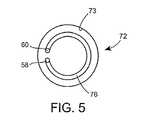
ベース72は、1つ以上の流路が形成される上部表面73を含む。図5は、円形の流路76を含むベース72の好適な実施形態を示す図である。液体は、入口58と供給ライン102を介して流路76に導入され、この液体は出口60と戻りライン104を介して液体源100に戻される。流路は、熱伝達部材48の温度制御を提供するために、ベース72の中に他の構成を持つことができる。例えば、流路は、らせん、ジグザグなどの他のパターンを代わりに持つことができる。
ベース72の流路は、例えば、半円形、円形、長方形、正方形、他の多角形などを含んだ、様々な横断面形状を持つことができる。流路の横断断面積は、流路を通る液体の所望の体積流量(volumetric flow rate)及び液体の熱伝達能力に基づいて、所望の体積の流路を提供するように選択されうる。好適な実施形態では、流路は、約1/32〜約3/32インチの幅、及び約1/32〜約1/16インチの深さを持つ。 The flow path of the base 72 can have various cross-sectional shapes including, for example, semi-circle, circle, rectangle, square, other polygons, and the like. The cross-sectional area of the flow path can be selected to provide a desired volume flow path based on the desired volumetric flow rate of the liquid through the flow path and the heat transfer capability of the liquid. In a preferred embodiment, the flow path has a width of about 1/32 to about 3/32 inches and a depth of about 1/32 to about 1/16 inches.
任意の適当な処理によって、ベース72内の流路が形成されうる。例えば、流路は、ベース72が機械加工処理などによって形成された後に、上部表面73内に形成されうる。また、流路は、例えば、キャスティング、型打ち、スタンピング又は他の処理などによって、本体を製造している間に形成されうる。 The flow path in the base 72 can be formed by any suitable process. For example, the flow path can be formed in the
液体は、水(例えば、脱イオン水)、エチレングリコール、シリコン油(silicon oil)、水/エチレングリコール混合物などであってもよい。液体の冷却性能は、液体流量及び/又は流路に導入される液体の温度を変化させて、異なる液体及び/又は異なる液体混合物を使用することによって、制御することができる。液体の温度は、好適には、液体源100によって調整することができる。 The liquid may be water (eg, deionized water), ethylene glycol, silicon oil, water / ethylene glycol mixtures, and the like. The cooling performance of the liquid can be controlled by using different liquids and / or different liquid mixtures by changing the liquid flow rate and / or the temperature of the liquid introduced into the flow path. The temperature of the liquid can preferably be adjusted by the
図2を参照すると、静電チャック50は、誘電体材料内に挟まれた導電性の電極(又は、二極動作(bipolaroperation)用の1組の電極)を含む。電極は、基板70をクランプするために設けられる。RFバイアスは、静電チャック50を通して基板70に容量結合される。熱伝達部材48は、好適には、カップリングの均一性を向上させる平たんな上面を有する。誘電体材料は、アルミナなどの適当なセラミック材料であってもよい。導電性の電極は、タングステンなどで作られうる。静電チャック50は、例えば、約1mmの厚さを持つことができる。静電チャック50は、その周辺エッジがセラミック材料46のフランジ64に接触するような幅を有する。従って、熱伝達部材48には直接的なRF経路が存在せず、アーク放電を防止している。誘電体材料は、基板70を支持するために静電チャックの露出表面を形成する。露出した表面は、好適には、ウェハの形状で基板70の形状に適合する円形である。 Referring to FIG. 2, the
図6に示される他の好適な実施形態では、セラミック部材146は、熱伝達部材48がその上に配置される平らな表面147(すなわち、凹んでいない表面)を有する。静電チャック50は、熱伝達部材48の上に位置する。ウェハ70は、静電チャック50の上に配置された状態で示されている。内側リング80は、表面147の上に配置され、熱伝達部材48、静電チャック50及びウェハ70を取り囲む。エッジリング52は、内側リング80を取り囲む。内側リング80は、好適には、セラミック部材146(例えば、アルミナ)と同じ材料で作られる。熱伝達部材48は、空間82によって内側リング80と横方向に間隔が空いている。静電チャック50は、内側リング80に接触する。 In another preferred embodiment shown in FIG. 6, the
静電チャック50は、好適には、エラストマー材料などの適当な接着物質で熱伝達部材48に結合される。接着剤は、好適には、その熱伝導率を向上させて、静電チャック50とその下に位置する熱伝達部材48との間に十分な熱伝達を提供するために、金属フィラー(metallic filler)などの材料を含む。例えば、接着剤は、その伝導率を向上させるために、少なくとも1つの金属又は金属合金の粒子(particles)を含むことができる。 The
上述したように、大きな金属冷却板(典型的には、アルミニウムで作られる)は、1 1/4インチ以上の厚さと対応する大きな熱質量を持つことができる。一方、熱伝達部材48は、好適には、その容積をこのような大きな冷却板の体積の約5-10%に等しい体積を持つ。熱伝達部材48の大きく低減された容積によって、所定量だけその温度の変化させるために、熱伝達部材48から除去されるか又は加えられる必要がある熱量は、このような大きな冷却板と比較して大幅に低減される。熱伝達部材48は、好適には、約0.25℃/秒から約2℃/秒の速度で、加熱及び/又は冷却することができる。これと比較して、大きい熱質量を持つ大きな冷却板は、約1℃/分以下と同じ程度の温度変化速度(temperature change rate)を提供する。熱伝達部材48は、好適には、プラズマ処理の間、約-20〜約80℃の範囲で温度を制御することができる。 As noted above, large metal cold plates (typically made of aluminum) can have a large thermal mass corresponding to a thickness of 1 1/4 inches or more. On the other hand, the
さらに、熱伝達部材48の小さい熱質量によって、熱伝達部材48を必要な温度に加熱及び/又は冷却するために、熱伝達部材48に供給される必要がある液体の体積流量は、大きな熱質量を持つ大きな冷却板を加熱及び/又は冷却するのに必要とされる液体流量に比べて大幅に低減される。 Furthermore, the volumetric flow rate of the liquid that needs to be supplied to the
基板支持体40の好適な実施形態は、液体源100、熱伝達ガス源150(図6)及びコントローラ200を含む。上述のように、液体源100(図2)は、液体を熱伝達部材48内の流路に供給する。液体源100は、選択された温度及び/又は流量で液体を流路に供給するために、熱電冷却装置(thermoelectricchiller)(例えば、ペルチェクーラー)、熱交換器などを備えることができる。液体源100は、適当なポンプ装置を備えることができる。冷却装置などは、好適には、液体源100から液体が流れる距離を低減するために、熱伝達部材48の近傍に配置され、それによって液体源の応答時間を低減することに加えて、加熱又は冷却される必要がある液体経路内の液体容積を低減する。 A preferred embodiment of the
熱伝達ガス源は、熱伝達ガスを熱伝達ガス通路に供給する。熱伝達ガスは、熱伝達ガス通路を通して、静電チャック50の露出した表面に流れる。そこでは、熱伝達ガスが、露出した表面に形成された開口部及び/又はチャンネル(不図示)を通して、基板70の露出した表面と裏面との間のインタフェース85に分配される(図6)。基板支持体の露出した表面を冷却させる領域を提供する適当な熱伝達ガス供給システムは、本願と同じ出願人による米国特許第5,609,720号に開示され、その全体は本願に参照により組み込まれる。熱伝達ガスは、プラズマ処理の間、基板から離れた熱を十分に伝達する熱伝達能力を有する任意のガスであってもよい。例えば、熱伝達ガスは、ヘリウムなどであってもよい。 The heat transfer gas source supplies heat transfer gas to the heat transfer gas passage. The heat transfer gas flows to the exposed surface of the
コントローラ200は、好適には、流路に供給される液体のパラメータを選択的に変化させる液体源の動作を制御し、熱伝達ガス通路に供給される熱伝達ガスのパラメータを選択的に変化させるために熱伝達ガス源150の動作を制御する。コントローラ200は、好適には、液体源100の動作を制御して、液体源によって流路に供給される液体の温度及び/又は流量を制御することができ、熱伝達ガス源150の動作を制御して、露出した表面における必要な温度を実現するためにインタフェース部に供給される熱伝達ガスの流量及び/又は圧力を制御することができる。 The
コントローラ200は、好適には、基板支持体40の1つ以上の選択された位置及び/又は基板上で(例えば、裏面で)温度を測定するために基板支持体40内に配置される1つ以上の温度センサ(不図示)から入力信号を受け取る。温度センサは、例えば、静電チャック50の露出した表面に最も近い位置で温度を測定するために配置することができる。温度センサは、好適には、熱伝達ガス源150の動作の制御に加えて、液体源100の動作のフィードバック制御を可能にするために、リアルタイムの温度測定を提供する。コントローラ200は、液体源100及び熱伝達ガス源150の動作をマニュアルで操作可能であるか又は自動的に制御するようにプログラムされうる。 The
基板支持体40は、その中でプラズマ・エッチング、物理気相成長、化学気相成長(CVD)、イオン注入及び/又はレジスト剥離を含む様々なプラズマ処理動作が実行されるプラズマ処理装置内で使用されうる。プラズマ処理動作は、半導体材料、誘電体材料及び金属材料を含む様々な基板材料に対して実行されうる。 The
基板支持体40は、様々な真空半導体処理の役に立つ、動的で近接した温度制御(dynamic、close temperature control)を提供することができる。例えば、これらの特性は、ゲート及びシャロートレンチ素子分離(“STI”)エッチング処理における正確でステップが変わりやすい温度制御に役に立つ。また、例えば、基板支持体40の温度は、エッチングの間、基板内に傾斜した側壁(tapering sidewalls)を形成するために、傾斜して変化され(ramped)てもよい(例えば、線形的に)。急速に基板温度を変化させる能力は、誘電体材料のエッチング処理などの様々な処理で役に立つ。そこでは、熱が基板から素早く取り除かれない場合には、使用される高電力密度によって急激なウェハ過剰温度状態(rapid wafer over-temperature conditions)を生じさせうる。 The
本発明は、その特定の実施形態を参照して詳細に説明したが、当業者であれば、添付した特許請求の範囲を逸脱しない限り、様々な変形及び修正がなされ、均等物が用いられうることが明らかであろう。 Although the invention has been described in detail with reference to specific embodiments thereof, those skilled in the art can make various variations and modifications and equivalents without departing from the scope of the appended claims. It will be clear.
Claims (31)
Translated fromJapaneseセラミック部材と、
前記セラミック部材の上に位置する金属熱伝達部材であって、最大約1/4インチの厚さを有し、かつ、当該熱伝達部材に加熱及び冷却の少なくとも一方を行うためにそれを通して液体が循環可能な少なくとも1つの流路を含む金属熱伝達部材と、
前記熱伝達部材の上に位置する静電チャックであって、プラズマ処理装置の反応室内で基板を支持するための支持表面を有する静電チャックと、
を備えることを特徴とする基板支持体。A substrate support used in a reaction chamber of a plasma processing apparatus,
A ceramic member;
A metal heat transfer member positioned over the ceramic member having a maximum thickness of about ¼ inch and through which liquid can be applied to heat and / or cool the heat transfer member. A metal heat transfer member including at least one flow path capable of circulation;
An electrostatic chuck located on the heat transfer member, the electrostatic chuck having a support surface for supporting a substrate in a reaction chamber of a plasma processing apparatus;
A substrate support comprising:
(i)前記少なくとも1つの流路を通して循環される前記液体の体積流量及び温度の少なくとも一方、並びに、(ii)前記支持表面と前記基板との間に供給される前記熱伝達ガスの流速及び圧力の少なくとも一方、のうち少なくとも一方を制御するように動作可能なコントローラと、
を更に備えることを特徴とする請求項4に記載の基板支持体。A heat transfer gas source operable to supply a heat transfer gas between the support surface and the substrate;
(I) at least one of a volumetric flow rate and temperature of the liquid circulated through the at least one flow path, and (ii) a flow rate and pressure of the heat transfer gas supplied between the support surface and the substrate. A controller operable to control at least one of at least one of
The substrate support according to claim 4, further comprising:
前記セラミック部材は、前記凹んだ表面で約1から4mmの厚さを有し、
前記熱伝達部材は、前記凹んだ表面の上に配置され、かつ、前記フランジから横方向に間隔が空けられ、
前記静電チャックは、前記フランジに接触することを特徴とする請求項1に記載の基板支持体。The ceramic member includes a recessed surface and a peripheral flange;
The ceramic member has a thickness of about 1 to 4 mm on the recessed surface;
The heat transfer member is disposed on the recessed surface and is laterally spaced from the flange;
The substrate support according to claim 1, wherein the electrostatic chuck is in contact with the flange.
前記熱伝達部材は、前記セラミックリングから横方向に間隔が空けられ、
前記静電チャックは、前記セラミックリングと接触することを特徴とする請求項1に記載の基板支持体。A ceramic ring positioned on the ceramic member and surrounding the heat transfer member and the electrostatic chuck;
The heat transfer member is laterally spaced from the ceramic ring;
The substrate support according to claim 1, wherein the electrostatic chuck is in contact with the ceramic ring.
前記熱伝達部材と前記静電チャックとの間のエラストマー接続部と、
を備えることを特徴とする請求項1に記載の基板支持体。An elastomer connection between the ceramic member and the heat transfer member;
An elastomer connection between the heat transfer member and the electrostatic chuck;
The substrate support according to claim 1, comprising:
プラズマ処理装置の反応室内で請求項1に記載の前記基板支持体の前記支持表面の上に基板を配置する工程と、
前記反応室内に処理ガスを導入する工程と、
前記反応室内の前記処理ガスからプラズマを生成する工程と、
前記基板を処理する工程と、
前記基板の処理の間に、前記熱伝達部材の温度を選択された温度に制御するために前記少なくとも1つの流路を通して液体を循環させる工程と、
を含むことを特徴とする方法。A method for thermally controlling a substrate in a plasma processing apparatus,
Disposing a substrate on the support surface of the substrate support according to claim 1 in a reaction chamber of a plasma processing apparatus;
Introducing a processing gas into the reaction chamber;
Generating plasma from the processing gas in the reaction chamber;
Processing the substrate;
Circulating a liquid through the at least one flow path to control the temperature of the heat transfer member to a selected temperature during processing of the substrate;
A method comprising the steps of:
前記基板の処理の間に、前記熱伝達部材の温度を第2の温度に制御するために前記少なくとも1つの流路を通して第2の温度を有する液体を循環させる工程と、
を含み、
前記熱伝達部材の温度は、(i)前記第1の温度から前記第2の温度に傾斜して変化されるか、又は、(ii)前記第1の温度から前記第2の温度に階段状に変化されることを特徴とする請求項13に記載の方法。Circulating a liquid having a first temperature through the at least one flow path to control the temperature of the heat transfer member to a first temperature during processing of the substrate;
Circulating a liquid having a second temperature through the at least one flow path to control the temperature of the heat transfer member to a second temperature during processing of the substrate;
Including
The temperature of the heat transfer member is changed (i) incline from the first temperature to the second temperature, or (ii) stepped from the first temperature to the second temperature. 14. The method of claim 13, wherein the method is changed to:
温度制御された液体源と、
セラミック部材と、
前記セラミック部材の上に位置する金属熱伝達部材であって、前記液体源と流体の伝達があり、かつ、約0.25から2℃/秒の速度で前記熱伝達部材に加熱及び冷却の少なくとも一方を行うためにそれを通して液体が循環可能な少なくとも1つの流路を含む金属熱伝達部材と、
前記熱伝達部材の上に位置する静電チャックであって、プラズマ処理装置の反応室内で基板を支持するための支持表面を有する静電チャックと、
を備えることを特徴とする基板支持体。A substrate support used in a plasma processing apparatus,
A temperature-controlled liquid source;
A ceramic member;
A metal heat transfer member positioned over the ceramic member, wherein the heat transfer member is in fluid communication with the liquid source and at least heating and cooling the heat transfer member at a rate of about 0.25 to 2 ° C / sec. A metal heat transfer member including at least one flow path through which liquid can circulate to perform one;
An electrostatic chuck located on the heat transfer member, the electrostatic chuck having a support surface for supporting a substrate in a reaction chamber of a plasma processing apparatus;
A substrate support comprising:
前記液体源及び前記熱伝達ガス源の動作を制御するように動作可能なコントローラと、
を更に備えることを特徴とする請求項15に記載の基板支持体。A heat transfer gas source operable to supply a heat transfer gas between the support surface and the substrate;
A controller operable to control operation of the liquid source and the heat transfer gas source;
The substrate support according to claim 15, further comprising:
前記熱伝達部材は、前記凹んだ表面の上に配置され、かつ、前記フランジから横方向に間隔が空けられ、
前記静電チャックは、前記フランジに接触することを特徴とする請求項15に記載の基板支持体。The ceramic member includes a recessed surface and a peripheral flange;
The heat transfer member is disposed on the recessed surface and is laterally spaced from the flange;
The substrate support according to claim 15, wherein the electrostatic chuck is in contact with the flange.
前記熱伝達部材は、前記セラミックリングから横方向に間隔が空けられ、
前記静電チャックは、前記セラミックリングと接触することを特徴とする請求項15に記載の基板支持体。A ceramic ring positioned on the ceramic member and surrounding the heat transfer member and the electrostatic chuck;
The heat transfer member is laterally spaced from the ceramic ring;
The substrate support according to claim 15, wherein the electrostatic chuck is in contact with the ceramic ring.
前記熱伝達部材と前記静電チャックとの間のエラストマー接続部と、
を備えることを特徴とする請求項15に記載の基板支持体。An elastomer connection between the ceramic member and the heat transfer member;
An elastomer connection between the heat transfer member and the electrostatic chuck;
The substrate support according to claim 15, comprising:
プラズマ処理装置の反応室内で請求項15に記載の前記基板支持体の前記支持表面の上に基板を配置する工程と、
前記反応室内に処理ガスを導入する工程と、
前記反応室内の前記処理ガスからプラズマを生成する工程と、
前記基板を処理する工程と、
前記基板の処理の間に、前記熱伝達部材の温度を選択された温度に制御するために前記少なくとも1つの流路を通して前記液体源から液体を循環させる工程と、
を含むことを特徴とする方法。A method for thermally controlling a substrate in a plasma processing apparatus,
Disposing a substrate on the support surface of the substrate support according to claim 15 in a reaction chamber of a plasma processing apparatus;
Introducing a processing gas into the reaction chamber;
Generating plasma from the processing gas in the reaction chamber;
Processing the substrate;
Circulating liquid from the liquid source through the at least one flow path to control the temperature of the heat transfer member to a selected temperature during processing of the substrate;
A method comprising the steps of:
前記基板の処理の間に、前記熱伝達部材の温度を第2の温度に制御するために前記少なくとも1つの流路を通して第2の温度を有する液体を循環させる工程と、
を含み、
前記熱伝達部材の温度は、(i)前記第1の温度から前記第2の温度に傾斜して変化されるか、又は、(ii)前記第1の温度から前記第2の温度に階段状に変化されることを特徴とする請求項24に記載の方法。Circulating a liquid having a first temperature through the at least one flow path to control the temperature of the heat transfer member to a first temperature during processing of the substrate;
Circulating a liquid having a second temperature through the at least one flow path to control the temperature of the heat transfer member to a second temperature during processing of the substrate;
Including
The temperature of the heat transfer member is changed (i) incline from the first temperature to the second temperature, or (ii) stepped from the first temperature to the second temperature. 25. The method of claim 24, wherein:
プラズマ処理装置の反応室内の静電チャックの支持表面の上で基板を支持する工程と、
前記基板をプラズマ処理する工程と、
前記基板の温度を制御するように前記静電チャックの下に位置する金属熱伝達部材を通して延びる少なくとも1つの流路を通して液体を循環させる工程と、
を含み、
前記熱伝達部材は、最大約1/4インチの厚さを有することを特徴とする方法。A method of processing a substrate in a plasma processing apparatus,
Supporting the substrate on the support surface of the electrostatic chuck in the reaction chamber of the plasma processing apparatus;
Plasma treating the substrate;
Circulating a liquid through at least one flow path extending through a metal heat transfer member located under the electrostatic chuck to control the temperature of the substrate;
Including
The heat transfer member has a maximum thickness of about 1/4 inch.
前記少なくとも1つの流路は、約1/32から約3/32インチまでの幅と、約1/32から約1/16インチまでの深さとを有することを特徴とする請求項26に記載の方法。The heat transfer member has a maximum thickness of about 1/8 inch;
27. The at least one flow path has a width of about 1/32 to about 3/32 inches and a depth of about 1/32 to about 1/16 inches. Method.
前記基板の処理の間に、前記熱伝達部材の温度を第2の温度に制御するために前記少なくとも1つの流路を通して第2の温度を有する液体を循環させる工程と、
を含み、
前記熱伝達部材の温度は、(i)前記第1の温度から前記第2の温度に傾斜して変化されるか、又は、(ii)前記第1の温度から前記第2の温度に階段状に変化されることを特徴とする請求項26に記載の方法。Circulating a liquid having a first temperature through the at least one flow path to control the temperature of the heat transfer member to a first temperature during processing of the substrate;
Circulating a liquid having a second temperature through the at least one flow path to control the temperature of the heat transfer member to a second temperature during processing of the substrate;
Including
The temperature of the heat transfer member is changed (i) incline from the first temperature to the second temperature, or (ii) stepped from the first temperature to the second temperature. 27. The method of claim 26, wherein the method is changed to:
Applications Claiming Priority (2)
| Application Number | Priority Date | Filing Date | Title |
|---|---|---|---|
| US10/608,091US7993460B2 (en) | 2003-06-30 | 2003-06-30 | Substrate support having dynamic temperature control |
| US10/608,091 | 2003-06-30 |
Related Parent Applications (1)
| Application Number | Title | Priority Date | Filing Date |
|---|---|---|---|
| JP2006517743ADivisionJP5053632B2 (en) | 2003-06-30 | 2004-06-28 | Substrate support, plasma processing apparatus, and method for thermally controlling a substrate in a plasma processing apparatus |
Publications (1)
| Publication Number | Publication Date |
|---|---|
| JP2012099825Atrue JP2012099825A (en) | 2012-05-24 |
Family
ID=33540476
Family Applications (2)
| Application Number | Title | Priority Date | Filing Date |
|---|---|---|---|
| JP2006517743AExpired - Fee RelatedJP5053632B2 (en) | 2003-06-30 | 2004-06-28 | Substrate support, plasma processing apparatus, and method for thermally controlling a substrate in a plasma processing apparatus |
| JP2011259478APendingJP2012099825A (en) | 2003-06-30 | 2011-11-28 | Substrate support having dynamic temperature control |
Family Applications Before (1)
| Application Number | Title | Priority Date | Filing Date |
|---|---|---|---|
| JP2006517743AExpired - Fee RelatedJP5053632B2 (en) | 2003-06-30 | 2004-06-28 | Substrate support, plasma processing apparatus, and method for thermally controlling a substrate in a plasma processing apparatus |
Country Status (8)
| Country | Link |
|---|---|
| US (2) | US7993460B2 (en) |
| EP (1) | EP1644962A4 (en) |
| JP (2) | JP5053632B2 (en) |
| KR (3) | KR101476566B1 (en) |
| CN (1) | CN100440422C (en) |
| MY (1) | MY151676A (en) |
| TW (1) | TWI338931B (en) |
| WO (1) | WO2005006400A2 (en) |
Cited By (2)
| Publication number | Priority date | Publication date | Assignee | Title |
|---|---|---|---|---|
| JP2019515506A (en)* | 2016-05-06 | 2019-06-06 | アプライド マテリアルズ インコーポレイテッドApplied Materials,Incorporated | Substrate support for whole area reverse flow heat exchange |
| KR20230161774A (en)* | 2022-05-19 | 2023-11-28 | 세메스 주식회사 | Substrate supporting apparatus and substrate processing apparatus including the same |
Families Citing this family (76)
| Publication number | Priority date | Publication date | Assignee | Title |
|---|---|---|---|---|
| WO2004095529A2 (en)* | 2003-03-21 | 2004-11-04 | Tokyo Electron Limited | Method and apparatus for reducing substrate backside deposition during processing |
| US7993460B2 (en) | 2003-06-30 | 2011-08-09 | Lam Research Corporation | Substrate support having dynamic temperature control |
| US6976782B1 (en)* | 2003-11-24 | 2005-12-20 | Lam Research Corporation | Methods and apparatus for in situ substrate temperature monitoring |
| US7544251B2 (en)* | 2004-10-07 | 2009-06-09 | Applied Materials, Inc. | Method and apparatus for controlling temperature of a substrate |
| US7648914B2 (en) | 2004-10-07 | 2010-01-19 | Applied Materials, Inc. | Method for etching having a controlled distribution of process results |
| US7436645B2 (en) | 2004-10-07 | 2008-10-14 | Applied Materials, Inc. | Method and apparatus for controlling temperature of a substrate |
| KR100899244B1 (en)* | 2005-03-03 | 2009-05-27 | 어플라이드 머티어리얼스, 인코포레이티드 | Method for etching having a controlled distribution of process results |
| JP4647401B2 (en) | 2005-06-06 | 2011-03-09 | 東京エレクトロン株式会社 | Substrate holder, substrate temperature control apparatus, and substrate temperature control method |
| US8226769B2 (en) | 2006-04-27 | 2012-07-24 | Applied Materials, Inc. | Substrate support with electrostatic chuck having dual temperature zones |
| US9275887B2 (en) | 2006-07-20 | 2016-03-01 | Applied Materials, Inc. | Substrate processing with rapid temperature gradient control |
| US7528392B2 (en) | 2006-11-27 | 2009-05-05 | Varian Semiconductor Equipment Associates, Inc. | Techniques for low-temperature ion implantation |
| JP4450245B2 (en)* | 2007-06-07 | 2010-04-14 | 株式会社デンソー | Manufacturing method of semiconductor device |
| TWI508129B (en)* | 2007-10-31 | 2015-11-11 | Lam Res Corp | Temperature control module using gas pressure to control thermal conductance between liquid coolant and component body |
| CN101903996B (en)* | 2007-12-21 | 2013-04-03 | 应用材料公司 | Method and apparatus for controlling temperature of a substrate |
| US8352015B2 (en)* | 2008-05-27 | 2013-01-08 | Kyma Medical Technologies, Ltd. | Location tracking of a metallic object in a living body using a radar detector and guiding an ultrasound probe to direct ultrasound waves at the location |
| US9265438B2 (en) | 2008-05-27 | 2016-02-23 | Kyma Medical Technologies Ltd. | Locating features in the heart using radio frequency imaging |
| US8989837B2 (en)* | 2009-12-01 | 2015-03-24 | Kyma Medical Technologies Ltd. | Methods and systems for determining fluid content of tissue |
| US20100116788A1 (en)* | 2008-11-12 | 2010-05-13 | Lam Research Corporation | Substrate temperature control by using liquid controlled multizone substrate support |
| US20100144140A1 (en)* | 2008-12-10 | 2010-06-10 | Novellus Systems, Inc. | Methods for depositing tungsten films having low resistivity for gapfill applications |
| US8129270B1 (en) | 2008-12-10 | 2012-03-06 | Novellus Systems, Inc. | Method for depositing tungsten film having low resistivity, low roughness and high reflectivity |
| US9548228B2 (en) | 2009-08-04 | 2017-01-17 | Lam Research Corporation | Void free tungsten fill in different sized features |
| US9034768B2 (en)* | 2010-07-09 | 2015-05-19 | Novellus Systems, Inc. | Depositing tungsten into high aspect ratio features |
| US8124531B2 (en) | 2009-08-04 | 2012-02-28 | Novellus Systems, Inc. | Depositing tungsten into high aspect ratio features |
| US10256142B2 (en) | 2009-08-04 | 2019-04-09 | Novellus Systems, Inc. | Tungsten feature fill with nucleation inhibition |
| US8410393B2 (en)* | 2010-05-24 | 2013-04-02 | Lam Research Corporation | Apparatus and method for temperature control of a semiconductor substrate support |
| US9220420B2 (en) | 2010-07-21 | 2015-12-29 | Kyma Medical Technologies Ltd. | Implantable dielectrometer |
| JP5781803B2 (en)* | 2011-03-30 | 2015-09-24 | 東京エレクトロン株式会社 | Temperature control method and plasma processing system |
| US8520360B2 (en) | 2011-07-19 | 2013-08-27 | Lam Research Corporation | Electrostatic chuck with wafer backside plasma assisted dechuck |
| US20130240144A1 (en)* | 2012-03-13 | 2013-09-19 | Applied Materials, Inc. | Fast response fluid temperature control system |
| TWI602283B (en) | 2012-03-27 | 2017-10-11 | 諾發系統有限公司 | Tungsten feature fill |
| US9132436B2 (en) | 2012-09-21 | 2015-09-15 | Applied Materials, Inc. | Chemical control features in wafer process equipment |
| US8970114B2 (en) | 2013-02-01 | 2015-03-03 | Lam Research Corporation | Temperature controlled window of a plasma processing chamber component |
| US9287147B2 (en) | 2013-03-14 | 2016-03-15 | Applied Materials, Inc. | Substrate support with advanced edge control provisions |
| US9082826B2 (en) | 2013-05-24 | 2015-07-14 | Lam Research Corporation | Methods and apparatuses for void-free tungsten fill in three-dimensional semiconductor features |
| JP6159172B2 (en)* | 2013-06-26 | 2017-07-05 | 東京エレクトロン株式会社 | Temperature control method and plasma processing apparatus |
| US9859145B2 (en) | 2013-07-17 | 2018-01-02 | Lam Research Corporation | Cooled pin lifter paddle for semiconductor substrate processing apparatus |
| US10680324B2 (en) | 2013-10-29 | 2020-06-09 | Zoll Medical Israel Ltd. | Antenna systems and devices and methods of manufacture thereof |
| US11013420B2 (en) | 2014-02-05 | 2021-05-25 | Zoll Medical Israel Ltd. | Systems, apparatuses and methods for determining blood pressure |
| US20150228514A1 (en)* | 2014-02-12 | 2015-08-13 | Axcelis Technologies, Inc. | Multi Fluid Cooling System for Large Temperature Range Chuck |
| US11259715B2 (en) | 2014-09-08 | 2022-03-01 | Zoll Medical Israel Ltd. | Monitoring and diagnostics systems and methods |
| US10548485B2 (en) | 2015-01-12 | 2020-02-04 | Zoll Medical Israel Ltd. | Systems, apparatuses and methods for radio frequency-based attachment sensing |
| US20160225652A1 (en) | 2015-02-03 | 2016-08-04 | Applied Materials, Inc. | Low temperature chuck for plasma processing systems |
| CN104835761A (en)* | 2015-04-27 | 2015-08-12 | 沈阳拓荆科技有限公司 | Temperature-controllable heating disc enabling peripheral outgassing |
| JP6655310B2 (en) | 2015-07-09 | 2020-02-26 | 株式会社日立ハイテクノロジーズ | Plasma processing equipment |
| US9741593B2 (en) | 2015-08-06 | 2017-08-22 | Applied Materials, Inc. | Thermal management systems and methods for wafer processing systems |
| TWI808334B (en)* | 2015-08-06 | 2023-07-11 | 美商應用材料股份有限公司 | Workpiece holder |
| US9972504B2 (en) | 2015-08-07 | 2018-05-15 | Lam Research Corporation | Atomic layer etching of tungsten for enhanced tungsten deposition fill |
| US9978610B2 (en) | 2015-08-21 | 2018-05-22 | Lam Research Corporation | Pulsing RF power in etch process to enhance tungsten gapfill performance |
| US10504700B2 (en) | 2015-08-27 | 2019-12-10 | Applied Materials, Inc. | Plasma etching systems and methods with secondary plasma injection |
| CN106637132B (en)* | 2015-10-29 | 2020-01-10 | 沈阳拓荆科技有限公司 | Wafer reaction table with circulating medium for automatic temperature control and heat conduction gas for temperature conduction |
| JP6697089B2 (en)* | 2016-03-18 | 2020-05-20 | エーシーエム リサーチ (シャンハイ) インコーポレーテッド | Substrate heat treatment equipment |
| US10504754B2 (en) | 2016-05-19 | 2019-12-10 | Applied Materials, Inc. | Systems and methods for improved semiconductor etching and component protection |
| US9865484B1 (en) | 2016-06-29 | 2018-01-09 | Applied Materials, Inc. | Selective etch using material modification and RF pulsing |
| US10566211B2 (en) | 2016-08-30 | 2020-02-18 | Lam Research Corporation | Continuous and pulsed RF plasma for etching metals |
| US10725485B2 (en)* | 2016-12-15 | 2020-07-28 | Lam Research Corporation | System and method for calculating substrate support temperature |
| US11276590B2 (en) | 2017-05-17 | 2022-03-15 | Applied Materials, Inc. | Multi-zone semiconductor substrate supports |
| JP7176860B6 (en) | 2017-05-17 | 2022-12-16 | アプライド マテリアルズ インコーポレイテッド | Semiconductor processing chamber to improve precursor flow |
| US11276559B2 (en) | 2017-05-17 | 2022-03-15 | Applied Materials, Inc. | Semiconductor processing chamber for multiple precursor flow |
| KR102439617B1 (en)* | 2017-06-27 | 2022-09-05 | 주식회사 미코세라믹스 | Bonding head and apparatus for bonding chips having the bonding head |
| US10199252B2 (en)* | 2017-06-30 | 2019-02-05 | Taiwan Semiconductor Manufacturing Company, Ltd. | Thermal pad for etch rate uniformity |
| US10297458B2 (en) | 2017-08-07 | 2019-05-21 | Applied Materials, Inc. | Process window widening using coated parts in plasma etch processes |
| US11020002B2 (en) | 2017-08-10 | 2021-06-01 | Zoll Medical Israel Ltd. | Systems, devices and methods for physiological monitoring of patients |
| US11328909B2 (en) | 2017-12-22 | 2022-05-10 | Applied Materials, Inc. | Chamber conditioning and removal processes |
| US11049755B2 (en) | 2018-09-14 | 2021-06-29 | Applied Materials, Inc. | Semiconductor substrate supports with embedded RF shield |
| US11062887B2 (en) | 2018-09-17 | 2021-07-13 | Applied Materials, Inc. | High temperature RF heater pedestals |
| US11682560B2 (en) | 2018-10-11 | 2023-06-20 | Applied Materials, Inc. | Systems and methods for hafnium-containing film removal |
| US10548239B1 (en)* | 2018-10-23 | 2020-01-28 | Google Llc | Cooling electronic devices in a data center |
| US11121002B2 (en) | 2018-10-24 | 2021-09-14 | Applied Materials, Inc. | Systems and methods for etching metals and metal derivatives |
| US11437242B2 (en) | 2018-11-27 | 2022-09-06 | Applied Materials, Inc. | Selective removal of silicon-containing materials |
| US12420314B2 (en)* | 2019-10-18 | 2025-09-23 | Taiwan Semiconductor Manufacturing Co., Ltd. | Semiconductor cleaning apparatus and method |
| CN112786422B (en)* | 2019-11-08 | 2024-03-12 | 中微半导体设备(上海)股份有限公司 | Focusing ring, plasma processor and method |
| CN111276430B (en)* | 2020-01-20 | 2023-02-14 | 北京北方华创微电子装备有限公司 | Temperature control device in semiconductor equipment and semiconductor equipment |
| CN111979530B (en)* | 2020-08-28 | 2022-10-18 | 湖南红太阳光电科技有限公司 | Heating system and heating control method of PECVD (plasma enhanced chemical vapor deposition) equipment and PECVD equipment |
| KR102572570B1 (en)* | 2021-07-02 | 2023-08-29 | 광운대학교 산학협력단 | Substrate processing apparatus and temperature control method using multi-zone heat transfer structure |
| TWI871537B (en)* | 2022-10-20 | 2025-02-01 | 張寶杰 | Planar external cooling device for wafer chamber, wafer chamber system and cooling method thereof |
| CN119314913A (en)* | 2024-12-17 | 2025-01-14 | 青岛四方思锐智能技术有限公司 | A method, system, device and storage medium for cooling a wafer boat box |
Citations (10)
| Publication number | Priority date | Publication date | Assignee | Title |
|---|---|---|---|---|
| JPH05226292A (en)* | 1992-02-13 | 1993-09-03 | Tokyo Electron Yamanashi Kk | Starting method for plasma-processing |
| JPH09291366A (en)* | 1996-04-26 | 1997-11-11 | Tokyo Electron Ltd | Plasma treatment and plasma treating device |
| JPH1074600A (en)* | 1996-05-02 | 1998-03-17 | Tokyo Electron Ltd | Plasma processing equipment |
| JPH1140654A (en)* | 1997-07-17 | 1999-02-12 | Kokusai Electric Co Ltd | Substrate holding structure |
| JP2000310459A (en)* | 1999-03-05 | 2000-11-07 | Samsung Electronics Co Ltd | Thermoelectric cooling temperature controller for semiconductor manufacturing process equipment |
| JP2001257253A (en)* | 2000-03-13 | 2001-09-21 | Hitachi Ltd | Wafer processing apparatus and wafer manufacturing method |
| JP2001267403A (en)* | 2000-03-21 | 2001-09-28 | Nhk Spring Co Ltd | Semiconductor wafer heating / cooling device |
| JP2001332608A (en)* | 2000-05-25 | 2001-11-30 | Sumitomo Heavy Ind Ltd | Cooling plate for wafer chuck and wafer chuck |
| JP2002353298A (en)* | 2001-05-23 | 2002-12-06 | Tokyo Electron Ltd | Mounting device |
| US6529686B2 (en)* | 2001-06-06 | 2003-03-04 | Fsi International, Inc. | Heating member for combination heating and chilling apparatus, and methods |
Family Cites Families (52)
| Publication number | Priority date | Publication date | Assignee | Title |
|---|---|---|---|---|
| JPS6060060A (en)* | 1983-09-12 | 1985-04-06 | 株式会社日立製作所 | Switchgear for door of railway rolling stock |
| US5225663A (en)* | 1988-06-15 | 1993-07-06 | Tel Kyushu Limited | Heat process device |
| JPH03190125A (en) | 1989-12-19 | 1991-08-20 | Fujitsu Ltd | Dry etching device |
| US5221403A (en)* | 1990-07-20 | 1993-06-22 | Tokyo Electron Limited | Support table for plate-like body and processing apparatus using the table |
| US5192849A (en)* | 1990-08-10 | 1993-03-09 | Texas Instruments Incorporated | Multipurpose low-thermal-mass chuck for semiconductor processing equipment |
| KR0164618B1 (en)* | 1992-02-13 | 1999-02-01 | 이노우에 쥰이치 | Plasma process method using an electrostatic chuck |
| KR100238629B1 (en)* | 1992-12-17 | 2000-01-15 | 히가시 데쓰로 | Stage having eletrostatic chuck and plasma processing apparatus using same |
| US6544379B2 (en)* | 1993-09-16 | 2003-04-08 | Hitachi, Ltd. | Method of holding substrate and substrate holding system |
| TW277139B (en)* | 1993-09-16 | 1996-06-01 | Hitachi Seisakusyo Kk | |
| US5900103A (en)* | 1994-04-20 | 1999-05-04 | Tokyo Electron Limited | Plasma treatment method and apparatus |
| US5548470A (en)* | 1994-07-19 | 1996-08-20 | International Business Machines Corporation | Characterization, modeling, and design of an electrostatic chuck with improved wafer temperature uniformity |
| US5671116A (en)* | 1995-03-10 | 1997-09-23 | Lam Research Corporation | Multilayered electrostatic chuck and method of manufacture thereof |
| US5609720A (en)* | 1995-09-29 | 1997-03-11 | Lam Research Corporation | Thermal control of semiconductor wafer during reactive ion etching |
| US6231776B1 (en)* | 1995-12-04 | 2001-05-15 | Daniel L. Flamm | Multi-temperature processing |
| US6108189A (en)* | 1996-04-26 | 2000-08-22 | Applied Materials, Inc. | Electrostatic chuck having improved gas conduits |
| EP0805475B1 (en) | 1996-05-02 | 2003-02-19 | Tokyo Electron Limited | Plasma processing apparatus |
| US6046439A (en)* | 1996-06-17 | 2000-04-04 | Mattson Technology, Inc. | System and method for thermal processing of a semiconductor substrate |
| US6170428B1 (en)* | 1996-07-15 | 2001-01-09 | Applied Materials, Inc. | Symmetric tunable inductively coupled HDP-CVD reactor |
| US5849076A (en)* | 1996-07-26 | 1998-12-15 | Memc Electronic Materials, Inc. | Cooling system and method for epitaxial barrel reactor |
| TW334609B (en)* | 1996-09-19 | 1998-06-21 | Hitachi Ltd | Electrostatic chuck, method and device for processing sanyle use the same |
| US5835334A (en)* | 1996-09-30 | 1998-11-10 | Lam Research | Variable high temperature chuck for high density plasma chemical vapor deposition |
| KR100430189B1 (en)* | 1996-10-11 | 2004-05-03 | 동경 엘렉트론 주식회사 | Plasma etching method |
| JPH10220909A (en)* | 1996-12-03 | 1998-08-21 | Komatsu Ltd | Fluid temperature control device |
| JPH10284360A (en)* | 1997-04-02 | 1998-10-23 | Hitachi Ltd | Substrate temperature control device and method |
| US6077357A (en)* | 1997-05-29 | 2000-06-20 | Applied Materials, Inc. | Orientless wafer processing on an electrostatic chuck |
| US6189483B1 (en)* | 1997-05-29 | 2001-02-20 | Applied Materials, Inc. | Process kit |
| US6083344A (en)* | 1997-05-29 | 2000-07-04 | Applied Materials, Inc. | Multi-zone RF inductively coupled source configuration |
| US6007635A (en)* | 1997-11-26 | 1999-12-28 | Micro C Technologies, Inc. | Platform for supporting a semiconductor substrate and method of supporting a substrate during rapid high temperature processing |
| US6138745A (en)* | 1997-09-26 | 2000-10-31 | Cvc Products, Inc. | Two-stage sealing system for thermally conductive chuck |
| US5983644A (en)* | 1997-09-29 | 1999-11-16 | Applied Materials, Inc. | Integrated bake and chill plate |
| JP3980187B2 (en)* | 1998-07-24 | 2007-09-26 | 日本碍子株式会社 | Semiconductor holding device, its manufacturing method and its use |
| US6280584B1 (en)* | 1998-07-29 | 2001-08-28 | Applied Materials, Inc. | Compliant bond structure for joining ceramic to metal |
| US6635580B1 (en)* | 1999-04-01 | 2003-10-21 | Taiwan Semiconductor Manufacturing Co. Ltd. | Apparatus and method for controlling wafer temperature in a plasma etcher |
| US6184504B1 (en)* | 1999-04-13 | 2001-02-06 | Silicon Thermal, Inc. | Temperature control system for electronic devices |
| US6179921B1 (en)* | 1999-04-19 | 2001-01-30 | Applied Materials, Inc. | Backside gas delivery system for a semiconductor wafer processing system |
| US6490146B2 (en)* | 1999-05-07 | 2002-12-03 | Applied Materials Inc. | Electrostatic chuck bonded to base with a bond layer and method |
| US6310755B1 (en)* | 1999-05-07 | 2001-10-30 | Applied Materials, Inc. | Electrostatic chuck having gas cavity and method |
| US6461801B1 (en)* | 1999-05-27 | 2002-10-08 | Matrix Integrated Systems, Inc. | Rapid heating and cooling of workpiece chucks |
| JP2001102435A (en)* | 1999-07-28 | 2001-04-13 | Tokyo Electron Ltd | Mounting table structure and treating apparatus |
| US6474986B2 (en)* | 1999-08-11 | 2002-11-05 | Tokyo Electron Limited | Hot plate cooling method and heat processing apparatus |
| US6451157B1 (en)* | 1999-09-23 | 2002-09-17 | Lam Research Corporation | Gas distribution apparatus for semiconductor processing |
| US6377437B1 (en)* | 1999-12-22 | 2002-04-23 | Lam Research Corporation | High temperature electrostatic chuck |
| KR20010111058A (en)* | 2000-06-09 | 2001-12-15 | 조셉 제이. 스위니 | Full area temperature controlled electrostatic chuck and method of fabricating same |
| WO2002017384A1 (en) | 2000-08-23 | 2002-02-28 | Applied Materials, Inc. | Electrostatic chuck temperature control method and system |
| JP3920015B2 (en)* | 2000-09-14 | 2007-05-30 | 東京エレクトロン株式会社 | Si substrate processing method |
| US6800173B2 (en)* | 2000-12-15 | 2004-10-05 | Novellus Systems, Inc. | Variable gas conductance control for a process chamber |
| JP4493863B2 (en)* | 2001-01-25 | 2010-06-30 | 東京エレクトロン株式会社 | Plasma processing apparatus, cleaning method thereof, and electrostatic chuck static elimination method |
| JP3971603B2 (en)* | 2001-12-04 | 2007-09-05 | キヤノンアネルバ株式会社 | Insulating film etching apparatus and insulating film etching method |
| JP4493251B2 (en)* | 2001-12-04 | 2010-06-30 | Toto株式会社 | Electrostatic chuck module and substrate processing apparatus |
| US20070051471A1 (en)* | 2002-10-04 | 2007-03-08 | Applied Materials, Inc. | Methods and apparatus for stripping |
| US20040163601A1 (en)* | 2003-02-26 | 2004-08-26 | Masanori Kadotani | Plasma processing apparatus |
| US7993460B2 (en) | 2003-06-30 | 2011-08-09 | Lam Research Corporation | Substrate support having dynamic temperature control |
- 2003
- 2003-06-30USUS10/608,091patent/US7993460B2/enactiveActive
- 2004
- 2004-06-28JPJP2006517743Apatent/JP5053632B2/ennot_activeExpired - Fee Related
- 2004-06-28KRKR1020137007852Apatent/KR101476566B1/ennot_activeExpired - Fee Related
- 2004-06-28CNCNB2004800216848Apatent/CN100440422C/ennot_activeExpired - Fee Related
- 2004-06-28WOPCT/US2004/020749patent/WO2005006400A2/enactiveApplication Filing
- 2004-06-28EPEP04777208Apatent/EP1644962A4/ennot_activeWithdrawn
- 2004-06-28KRKR1020057025443Apatent/KR20060025586A/ennot_activeCeased
- 2004-06-28KRKR1020127014042Apatent/KR20120066683A/ennot_activeCeased
- 2004-06-29MYMYPI20042581patent/MY151676A/enunknown
- 2004-06-29TWTW093119132Apatent/TWI338931B/ennot_activeIP Right Cessation
- 2011
- 2011-06-24USUS13/168,134patent/US8747559B2/ennot_activeExpired - Fee Related
- 2011-11-28JPJP2011259478Apatent/JP2012099825A/enactivePending
Patent Citations (10)
| Publication number | Priority date | Publication date | Assignee | Title |
|---|---|---|---|---|
| JPH05226292A (en)* | 1992-02-13 | 1993-09-03 | Tokyo Electron Yamanashi Kk | Starting method for plasma-processing |
| JPH09291366A (en)* | 1996-04-26 | 1997-11-11 | Tokyo Electron Ltd | Plasma treatment and plasma treating device |
| JPH1074600A (en)* | 1996-05-02 | 1998-03-17 | Tokyo Electron Ltd | Plasma processing equipment |
| JPH1140654A (en)* | 1997-07-17 | 1999-02-12 | Kokusai Electric Co Ltd | Substrate holding structure |
| JP2000310459A (en)* | 1999-03-05 | 2000-11-07 | Samsung Electronics Co Ltd | Thermoelectric cooling temperature controller for semiconductor manufacturing process equipment |
| JP2001257253A (en)* | 2000-03-13 | 2001-09-21 | Hitachi Ltd | Wafer processing apparatus and wafer manufacturing method |
| JP2001267403A (en)* | 2000-03-21 | 2001-09-28 | Nhk Spring Co Ltd | Semiconductor wafer heating / cooling device |
| JP2001332608A (en)* | 2000-05-25 | 2001-11-30 | Sumitomo Heavy Ind Ltd | Cooling plate for wafer chuck and wafer chuck |
| JP2002353298A (en)* | 2001-05-23 | 2002-12-06 | Tokyo Electron Ltd | Mounting device |
| US6529686B2 (en)* | 2001-06-06 | 2003-03-04 | Fsi International, Inc. | Heating member for combination heating and chilling apparatus, and methods |
Cited By (4)
| Publication number | Priority date | Publication date | Assignee | Title |
|---|---|---|---|---|
| JP2019515506A (en)* | 2016-05-06 | 2019-06-06 | アプライド マテリアルズ インコーポレイテッドApplied Materials,Incorporated | Substrate support for whole area reverse flow heat exchange |
| US10648080B2 (en) | 2016-05-06 | 2020-05-12 | Applied Materials, Inc. | Full-area counter-flow heat exchange substrate support |
| KR20230161774A (en)* | 2022-05-19 | 2023-11-28 | 세메스 주식회사 | Substrate supporting apparatus and substrate processing apparatus including the same |
| KR102721404B1 (en) | 2022-05-19 | 2024-10-25 | 세메스 주식회사 | Substrate supporting apparatus and substrate processing apparatus including the same |
Also Published As
| Publication number | Publication date |
|---|---|
| WO2005006400A2 (en) | 2005-01-20 |
| CN1849697A (en) | 2006-10-18 |
| KR20120066683A (en) | 2012-06-22 |
| KR20060025586A (en) | 2006-03-21 |
| US20040261721A1 (en) | 2004-12-30 |
| US8747559B2 (en) | 2014-06-10 |
| KR20130049819A (en) | 2013-05-14 |
| JP2007529102A (en) | 2007-10-18 |
| JP5053632B2 (en) | 2012-10-17 |
| TW200507158A (en) | 2005-02-16 |
| US7993460B2 (en) | 2011-08-09 |
| WO2005006400A3 (en) | 2006-04-13 |
| CN100440422C (en) | 2008-12-03 |
| US20110262315A1 (en) | 2011-10-27 |
| KR101476566B1 (en) | 2014-12-24 |
| EP1644962A4 (en) | 2010-11-17 |
| MY151676A (en) | 2014-06-30 |
| EP1644962A2 (en) | 2006-04-12 |
| TWI338931B (en) | 2011-03-11 |
Similar Documents
| Publication | Publication Date | Title |
|---|---|---|
| JP5053632B2 (en) | Substrate support, plasma processing apparatus, and method for thermally controlling a substrate in a plasma processing apparatus | |
| US8921740B2 (en) | Method and apparatus for controlling the spatial temperature distribution across the surface of a workpiece support | |
| JP7551765B2 (en) | Sheath and temperature control of a process kit in a substrate processing chamber - Patents.com | |
| JP5006200B2 (en) | Heat transfer system for improving semiconductor processing uniformity. | |
| JP4970679B2 (en) | Plasma reaction chamber component with improved temperature uniformity and processing method using the same | |
| JP4745961B2 (en) | Substrate support having temperature-controlled substrate support surface, control method thereof, semiconductor processing apparatus and method | |
| KR100757545B1 (en) | Upper electrode and plasma processing apparatus | |
| US6302966B1 (en) | Temperature control system for plasma processing apparatus | |
| JP2008522446A (en) | Method and apparatus for controlling spatial temperature distribution | |
| KR20040015208A (en) | Method and apparatus for controlling the spatial temperature distribution across the surface of a workpiece support | |
| JP2014222786A (en) | Temperature controlled hot edge ring assembly | |
| EP1230663A1 (en) | Temperature control system for plasma processing apparatus | |
| US20030089457A1 (en) | Apparatus for controlling a thermal conductivity profile for a pedestal in a semiconductor wafer processing chamber | |
| KR20210004056A (en) | Shower head unit and system for treating substrate with the shower head unit | |
| CN110867363A (en) | Plasma processing apparatus | |
| JPH08181195A (en) | Improved heat transfer between pedestal and base | |
| CN115485807A (en) | Method and apparatus for processing substrate | |
| KR20200139259A (en) | Methods, apparatuses, and systems for substrate processing to lower contact resistance | |
| JP4471514B2 (en) | Plasma processing equipment |
Legal Events
| Date | Code | Title | Description |
|---|---|---|---|
| A977 | Report on retrieval | Free format text:JAPANESE INTERMEDIATE CODE: A971007 Effective date:20130129 | |
| A131 | Notification of reasons for refusal | Free format text:JAPANESE INTERMEDIATE CODE: A131 Effective date:20130204 | |
| A02 | Decision of refusal | Free format text:JAPANESE INTERMEDIATE CODE: A02 Effective date:20130628 |