JP2012098321A - Liquid crystal light control element and imaging apparatus - Google Patents
Liquid crystal light control element and imaging apparatusDownload PDFInfo
- Publication number
- JP2012098321A JP2012098321AJP2010243257AJP2010243257AJP2012098321AJP 2012098321 AJP2012098321 AJP 2012098321AJP 2010243257 AJP2010243257 AJP 2010243257AJP 2010243257 AJP2010243257 AJP 2010243257AJP 2012098321 AJP2012098321 AJP 2012098321A
- Authority
- JP
- Japan
- Prior art keywords
- liquid crystal
- light
- alignment
- light control
- crystal layer
- Prior art date
- Legal status (The legal status is an assumption and is not a legal conclusion. Google has not performed a legal analysis and makes no representation as to the accuracy of the status listed.)
- Granted
Links
- 239000004973liquid crystal related substanceSubstances0.000titleclaimsabstractdescription336
- 238000003384imaging methodMethods0.000titledescription66
- 238000000034methodMethods0.000claimsdescription31
- 230000008569processEffects0.000claimsdescription28
- 238000005192partitionMethods0.000claimsdescription23
- 239000000758substrateSubstances0.000claimsdescription22
- 239000011248coating agentSubstances0.000abstract1
- 238000000576coating methodMethods0.000abstract1
- 239000010410layerSubstances0.000description115
- 239000010408filmSubstances0.000description104
- 238000002834transmittanceMethods0.000description45
- 230000003287optical effectEffects0.000description37
- 230000000052comparative effectEffects0.000description25
- 238000010586diagramMethods0.000description14
- 230000004048modificationEffects0.000description12
- 238000012986modificationMethods0.000description12
- 238000007789sealingMethods0.000description12
- 239000000975dyeSubstances0.000description10
- 210000004027cellAnatomy0.000description7
- 238000012545processingMethods0.000description6
- 238000005452bendingMethods0.000description5
- 230000008859changeEffects0.000description4
- 210000002858crystal cellAnatomy0.000description4
- 230000007423decreaseEffects0.000description4
- 239000000463materialSubstances0.000description4
- 230000004044responseEffects0.000description4
- 125000006850spacer groupChemical group0.000description4
- 239000003795chemical substances by applicationSubstances0.000description3
- 230000002829reductive effectEffects0.000description3
- 239000003522acrylic cementSubstances0.000description2
- 239000000853adhesiveSubstances0.000description2
- 230000001070adhesive effectEffects0.000description2
- 230000005540biological transmissionEffects0.000description2
- 238000012937correctionMethods0.000description2
- 230000003247decreasing effectEffects0.000description2
- 230000000694effectsEffects0.000description2
- 229920006332epoxy adhesivePolymers0.000description2
- 239000011521glassSubstances0.000description2
- 239000012788optical filmSubstances0.000description2
- 230000035699permeabilityEffects0.000description2
- 239000004065semiconductorSubstances0.000description2
- 239000002356single layerSubstances0.000description2
- 239000004642PolyimideSubstances0.000description1
- BQCADISMDOOEFD-UHFFFAOYSA-NSilverChemical compound[Ag]BQCADISMDOOEFD-UHFFFAOYSA-N0.000description1
- 230000009471actionEffects0.000description1
- 239000000654additiveSubstances0.000description1
- 230000000996additive effectEffects0.000description1
- 230000002411adverseEffects0.000description1
- 239000000956alloySubstances0.000description1
- 229910045601alloyInorganic materials0.000description1
- 229910052782aluminiumInorganic materials0.000description1
- XAGFODPZIPBFFR-UHFFFAOYSA-NaluminiumChemical compound[Al]XAGFODPZIPBFFR-UHFFFAOYSA-N0.000description1
- 230000015572biosynthetic processEffects0.000description1
- 230000000295complement effectEffects0.000description1
- 239000000470constituentSubstances0.000description1
- 239000013078crystalSubstances0.000description1
- AMGQUBHHOARCQH-UHFFFAOYSA-Nindium;oxotinChemical compound[In].[Sn]=OAMGQUBHHOARCQH-UHFFFAOYSA-N0.000description1
- 229910010272inorganic materialInorganic materials0.000description1
- 239000011147inorganic materialSubstances0.000description1
- 238000003780insertionMethods0.000description1
- 230000037431insertionEffects0.000description1
- 229910052751metalInorganic materials0.000description1
- 239000002184metalSubstances0.000description1
- 229910044991metal oxideInorganic materials0.000description1
- 150000004706metal oxidesChemical class0.000description1
- 239000000203mixtureSubstances0.000description1
- 230000036961partial effectEffects0.000description1
- 239000000049pigmentSubstances0.000description1
- 230000010287polarizationEffects0.000description1
- 229920001721polyimidePolymers0.000description1
- 239000002861polymer materialSubstances0.000description1
- 238000012827research and developmentMethods0.000description1
- 229920005989resinPolymers0.000description1
- 239000011347resinSubstances0.000description1
- 239000000565sealantSubstances0.000description1
- 239000003566sealing materialSubstances0.000description1
- 229910052709silverInorganic materials0.000description1
- 239000004332silverSubstances0.000description1
- 230000003313weakening effectEffects0.000description1
Images


Classifications
- G—PHYSICS
- G02—OPTICS
- G02F—OPTICAL DEVICES OR ARRANGEMENTS FOR THE CONTROL OF LIGHT BY MODIFICATION OF THE OPTICAL PROPERTIES OF THE MEDIA OF THE ELEMENTS INVOLVED THEREIN; NON-LINEAR OPTICS; FREQUENCY-CHANGING OF LIGHT; OPTICAL LOGIC ELEMENTS; OPTICAL ANALOGUE/DIGITAL CONVERTERS
- G02F1/00—Devices or arrangements for the control of the intensity, colour, phase, polarisation or direction of light arriving from an independent light source, e.g. switching, gating or modulating; Non-linear optics
- G02F1/01—Devices or arrangements for the control of the intensity, colour, phase, polarisation or direction of light arriving from an independent light source, e.g. switching, gating or modulating; Non-linear optics for the control of the intensity, phase, polarisation or colour
- G02F1/13—Devices or arrangements for the control of the intensity, colour, phase, polarisation or direction of light arriving from an independent light source, e.g. switching, gating or modulating; Non-linear optics for the control of the intensity, phase, polarisation or colour based on liquid crystals, e.g. single liquid crystal display cells
- G02F1/133—Constructional arrangements; Operation of liquid crystal cells; Circuit arrangements
- G02F1/1333—Constructional arrangements; Manufacturing methods
- G02F1/1347—Arrangement of liquid crystal layers or cells in which the final condition of one light beam is achieved by the addition of the effects of two or more layers or cells
- G—PHYSICS
- G02—OPTICS
- G02F—OPTICAL DEVICES OR ARRANGEMENTS FOR THE CONTROL OF LIGHT BY MODIFICATION OF THE OPTICAL PROPERTIES OF THE MEDIA OF THE ELEMENTS INVOLVED THEREIN; NON-LINEAR OPTICS; FREQUENCY-CHANGING OF LIGHT; OPTICAL LOGIC ELEMENTS; OPTICAL ANALOGUE/DIGITAL CONVERTERS
- G02F1/00—Devices or arrangements for the control of the intensity, colour, phase, polarisation or direction of light arriving from an independent light source, e.g. switching, gating or modulating; Non-linear optics
- G02F1/01—Devices or arrangements for the control of the intensity, colour, phase, polarisation or direction of light arriving from an independent light source, e.g. switching, gating or modulating; Non-linear optics for the control of the intensity, phase, polarisation or colour
- G02F1/13—Devices or arrangements for the control of the intensity, colour, phase, polarisation or direction of light arriving from an independent light source, e.g. switching, gating or modulating; Non-linear optics for the control of the intensity, phase, polarisation or colour based on liquid crystals, e.g. single liquid crystal display cells
- G02F1/133—Constructional arrangements; Operation of liquid crystal cells; Circuit arrangements
- G02F1/1333—Constructional arrangements; Manufacturing methods
- G02F1/1335—Structural association of cells with optical devices, e.g. polarisers or reflectors
- G02F1/133553—Reflecting elements
- G—PHYSICS
- G02—OPTICS
- G02F—OPTICAL DEVICES OR ARRANGEMENTS FOR THE CONTROL OF LIGHT BY MODIFICATION OF THE OPTICAL PROPERTIES OF THE MEDIA OF THE ELEMENTS INVOLVED THEREIN; NON-LINEAR OPTICS; FREQUENCY-CHANGING OF LIGHT; OPTICAL LOGIC ELEMENTS; OPTICAL ANALOGUE/DIGITAL CONVERTERS
- G02F1/00—Devices or arrangements for the control of the intensity, colour, phase, polarisation or direction of light arriving from an independent light source, e.g. switching, gating or modulating; Non-linear optics
- G02F1/01—Devices or arrangements for the control of the intensity, colour, phase, polarisation or direction of light arriving from an independent light source, e.g. switching, gating or modulating; Non-linear optics for the control of the intensity, phase, polarisation or colour
- G02F1/13—Devices or arrangements for the control of the intensity, colour, phase, polarisation or direction of light arriving from an independent light source, e.g. switching, gating or modulating; Non-linear optics for the control of the intensity, phase, polarisation or colour based on liquid crystals, e.g. single liquid crystal display cells
- G02F1/133—Constructional arrangements; Operation of liquid crystal cells; Circuit arrangements
- G02F1/1333—Constructional arrangements; Manufacturing methods
- G02F1/1347—Arrangement of liquid crystal layers or cells in which the final condition of one light beam is achieved by the addition of the effects of two or more layers or cells
- G02F1/13475—Arrangement of liquid crystal layers or cells in which the final condition of one light beam is achieved by the addition of the effects of two or more layers or cells in which at least one liquid crystal cell or layer is doped with a pleochroic dye, e.g. GH-LC cell
- G—PHYSICS
- G03—PHOTOGRAPHY; CINEMATOGRAPHY; ANALOGOUS TECHNIQUES USING WAVES OTHER THAN OPTICAL WAVES; ELECTROGRAPHY; HOLOGRAPHY
- G03B—APPARATUS OR ARRANGEMENTS FOR TAKING PHOTOGRAPHS OR FOR PROJECTING OR VIEWING THEM; APPARATUS OR ARRANGEMENTS EMPLOYING ANALOGOUS TECHNIQUES USING WAVES OTHER THAN OPTICAL WAVES; ACCESSORIES THEREFOR
- G03B11/00—Filters or other obturators specially adapted for photographic purposes
- G—PHYSICS
- G03—PHOTOGRAPHY; CINEMATOGRAPHY; ANALOGOUS TECHNIQUES USING WAVES OTHER THAN OPTICAL WAVES; ELECTROGRAPHY; HOLOGRAPHY
- G03B—APPARATUS OR ARRANGEMENTS FOR TAKING PHOTOGRAPHS OR FOR PROJECTING OR VIEWING THEM; APPARATUS OR ARRANGEMENTS EMPLOYING ANALOGOUS TECHNIQUES USING WAVES OTHER THAN OPTICAL WAVES; ACCESSORIES THEREFOR
- G03B17/00—Details of cameras or camera bodies; Accessories therefor
- G03B17/02—Bodies
- G03B17/17—Bodies with reflectors arranged in beam forming the photographic image, e.g. for reducing dimensions of camera
- G—PHYSICS
- G02—OPTICS
- G02F—OPTICAL DEVICES OR ARRANGEMENTS FOR THE CONTROL OF LIGHT BY MODIFICATION OF THE OPTICAL PROPERTIES OF THE MEDIA OF THE ELEMENTS INVOLVED THEREIN; NON-LINEAR OPTICS; FREQUENCY-CHANGING OF LIGHT; OPTICAL LOGIC ELEMENTS; OPTICAL ANALOGUE/DIGITAL CONVERTERS
- G02F1/00—Devices or arrangements for the control of the intensity, colour, phase, polarisation or direction of light arriving from an independent light source, e.g. switching, gating or modulating; Non-linear optics
- G02F1/01—Devices or arrangements for the control of the intensity, colour, phase, polarisation or direction of light arriving from an independent light source, e.g. switching, gating or modulating; Non-linear optics for the control of the intensity, phase, polarisation or colour
- G02F1/13—Devices or arrangements for the control of the intensity, colour, phase, polarisation or direction of light arriving from an independent light source, e.g. switching, gating or modulating; Non-linear optics for the control of the intensity, phase, polarisation or colour based on liquid crystals, e.g. single liquid crystal display cells
- G02F1/133—Constructional arrangements; Operation of liquid crystal cells; Circuit arrangements
- G02F1/1333—Constructional arrangements; Manufacturing methods
- G02F1/1337—Surface-induced orientation of the liquid crystal molecules, e.g. by alignment layers
- G02F1/133753—Surface-induced orientation of the liquid crystal molecules, e.g. by alignment layers with different alignment orientations or pretilt angles on a same surface, e.g. for grey scale or improved viewing angle
- G02F1/133757—Surface-induced orientation of the liquid crystal molecules, e.g. by alignment layers with different alignment orientations or pretilt angles on a same surface, e.g. for grey scale or improved viewing angle with different alignment orientations
Landscapes
- Physics & Mathematics (AREA)
- Nonlinear Science (AREA)
- General Physics & Mathematics (AREA)
- Mathematical Physics (AREA)
- Chemical & Material Sciences (AREA)
- Crystallography & Structural Chemistry (AREA)
- Optics & Photonics (AREA)
- Liquid Crystal (AREA)
- Structure And Mechanism Of Cameras (AREA)
- Optical Elements Other Than Lenses (AREA)
- Blocking Light For Cameras (AREA)
- Studio Devices (AREA)
Abstract
Description
Translated fromJapanese本発明は、液晶を用いて調光を行う液晶調光素子およびそのような液晶調光素子を備えた撮像装置に関する。 The present invention relates to a liquid crystal light control element that performs light control using liquid crystal, and an imaging apparatus including such a liquid crystal light control element.
外部から印加される電圧の程度に応じて光を反射する電気調光素子が多数提案されており(例えば、特許文献1)、中でも、液晶調光素子はその構造や制御方法が単純であることから注目されている。 Many electric dimmer elements that reflect light according to the level of voltage applied from the outside have been proposed (for example, Patent Document 1). Among them, the liquid crystal dimmer element has a simple structure and control method. Has been attracting attention.
液晶調光素子は、主に偏光板および液晶分子と二色性染料分子(色素)とを含むゲスト−ホスト(GH)セルから構成される。偏光板を透過した光は、ゲスト−ホストセルへと入射する。このとき液晶分子の長軸方向が光の進行方向となす角度が小さいと、出射側の光透過量が相対的に多く(光透過率が高く)なり、液晶分子の長軸方向がこの光の進行方向となす角度が直角に近いと、出射側の光透過量が相対的に少なく(光透過率が低く)なる。 The liquid crystal light control device is mainly composed of a polarizing plate and a guest-host (GH) cell containing liquid crystal molecules and dichroic dye molecules (pigments). The light transmitted through the polarizing plate enters the guest-host cell. At this time, if the angle between the long axis direction of the liquid crystal molecules and the light traveling direction is small, the light transmission amount on the emission side is relatively large (the light transmittance is high), and the long axis direction of the liquid crystal molecules is When the angle formed with the traveling direction is close to a right angle, the light transmission amount on the emission side is relatively small (light transmittance is low).
なお、液晶分子はネガ型とポジ型の2種に大別される。ネガ型は電圧無印加時に光軸方向と液晶分子の長軸方向とが平行となり、電圧印加時に光軸方向と液晶分子の長軸方向とが垂直となる。二色性染料分子は液晶分子と同方向に配列する。よって、ネガ型の液晶分子をホストとして用いた場合、電圧無印加時に光透過率が相対的に高く(明るく)、電圧印加時に光透過率が相対的に低く(暗く)なる。 Liquid crystal molecules are roughly classified into two types, negative and positive. In the negative type, when no voltage is applied, the optical axis direction and the major axis direction of the liquid crystal molecules are parallel, and when the voltage is applied, the optical axis direction and the major axis direction of the liquid crystal molecules are perpendicular. The dichroic dye molecules are aligned in the same direction as the liquid crystal molecules. Therefore, when negative liquid crystal molecules are used as a host, the light transmittance is relatively high (bright) when no voltage is applied, and the light transmittance is relatively low (dark) when a voltage is applied.
一方、ポジ型の液晶分子は、電圧無印加時および電圧印加時の液晶分子の配列がネガ型と逆となるため、ポジ型の液晶分子をホストとして用いた場合、電圧無印加時に光透過率が相対的に低く(暗く)、電圧印加時に光透過率が相対的に高く(明るく)なる。 On the other hand, in the case of positive type liquid crystal molecules, the alignment of the liquid crystal molecules when no voltage is applied and when the voltage is applied is opposite to the negative type. Therefore, when positive type liquid crystal molecules are used as a host, light transmittance is obtained when no voltage is applied. Is relatively low (dark), and light transmittance is relatively high (bright) when a voltage is applied.
ところで、このような調光素子では、撮像装置等の様々な電子機器へと適用されることから光透過率の差(遮光度合い)を表す調光範囲(調光レンジ,ダイナミックレンジ)が広いものが求められる。 By the way, in such a light control element, since it is applied to various electronic devices such as an imaging device, a light control range (light control range, dynamic range) indicating a difference in light transmittance (light shielding degree) is wide. Is required.
しかしながら、これまでの液晶調光素子の調光範囲は十分なものではなく、また、調光範囲を更に広げるための研究開発も活発になされていなかった。 However, the light control range of the liquid crystal light control device so far is not sufficient, and research and development for further expanding the light control range has not been made actively.
本発明はかかる問題点に鑑みてなされたもので、その目的は、幅広い調光範囲を有する液晶調光素子およびこの液晶調光素子を用いた撮像装置を提供することにある。 The present invention has been made in view of such problems, and an object thereof is to provide a liquid crystal light adjusting device having a wide light control range and an imaging apparatus using the liquid crystal light adjusting device.
本発明による液晶調光素子は、一方の面から光が入射する第1液晶層と、第1液晶層を透過する光を反射する反射膜とを備え、第1液晶層は隣接する配向領域を有し、隣接する配向領域間の液晶分子の配向方向が異なっているものである。 The liquid crystal light control device according to the present invention includes a first liquid crystal layer on which light is incident from one surface and a reflective film that reflects light transmitted through the first liquid crystal layer, and the first liquid crystal layer includes adjacent alignment regions. And having different alignment directions of liquid crystal molecules between adjacent alignment regions.
本発明の液晶調光素子では、液晶層の一方の面から入射した光と、反射膜により反射され、再び液晶層を透過する光とは、通過する配向領域の液晶分子の配向方向が少なくとも一部異なる。 In the liquid crystal light control device of the present invention, the light incident from one surface of the liquid crystal layer and the light reflected by the reflective film and transmitted again through the liquid crystal layer have at least one alignment direction of the liquid crystal molecules in the alignment region passing therethrough. Different parts.
本発明による撮像装置は、上記本発明の液晶調光素子を備えたものであり、当該液晶調光素子によって調光され、撮像が行われる。 An image pickup apparatus according to the present invention includes the liquid crystal light adjusting element of the present invention, and the light is adjusted by the liquid crystal light adjusting element to perform image pickup.
本発明の液晶調光素子および撮像装置によれば、第1液晶層を透過する光を反射する反射膜を設けると共に液晶層が液晶分子の配向方向が異なる配向領域を有するようにしたため、液晶層の一方の面から入射した光の進行方向と液晶分子の長軸方向とのなす角度および反射膜から反射された光の進行方向と液晶分子の長軸方向とのなす角度を共に制御することができる。よって、液晶調光素子の調光範囲を拡大することが可能となる。 According to the liquid crystal light control device and the imaging device of the present invention, the liquid crystal layer is provided with the reflective film that reflects the light transmitted through the first liquid crystal layer and the liquid crystal layer has alignment regions in which the alignment directions of the liquid crystal molecules are different. The angle between the traveling direction of light incident from one surface of the liquid crystal and the major axis direction of the liquid crystal molecules and the angle between the traveling direction of light reflected from the reflective film and the major axis direction of the liquid crystal molecules can be controlled together. it can. Therefore, the light control range of the liquid crystal light control element can be expanded.
以下、本発明の実施の形態について、図面を参照して詳細に説明する。なお、説明は以下の順序で行う。
1.第1の実施の形態(液晶分子の配向方向が異なる配向領域を有する液晶調光素子の例)
2.変形例(ラビング処理の方向についての変形例)
3.第2の実施の形態(複数の液晶層が積層されてなる液晶調光素子の例)Hereinafter, embodiments of the present invention will be described in detail with reference to the drawings. The description will be given in the following order.
1. First embodiment (an example of a liquid crystal light control device having alignment regions in which the alignment directions of liquid crystal molecules are different)
2. Modified example (modified example of rubbing direction)
3. Second embodiment (an example of a liquid crystal light control device in which a plurality of liquid crystal layers are stacked)
〔第1の実施の形態〕
[撮像装置1の全体構成]
図1は、本発明の第1の実施の形態に係る液晶調光素子(後述する液晶調光素子26)が適用された撮像装置(撮像装置1)の全体構成(外観構成)を斜視図で表したものである。この撮像装置1は、被写体からの光学的な画像を撮像素子(後述する撮像素子3)によって電気的な信号に変換するデジタルカメラ(デジタルスチルカメラ)である。なお、このようにして得られた撮像信号(デジタル信号)は、半導体記録メディア(図示せず)に記録したり、液晶ディスプレイ等の表示装置(図示せず)に表示したりすることが可能となっている。[First Embodiment]
[Overall Configuration of Imaging Device 1]
FIG. 1 is a perspective view of the overall configuration (appearance configuration) of an imaging apparatus (imaging apparatus 1) to which a liquid crystal light control element (a liquid crystal
撮像装置1では、本体部10(筐体)上に、レンズ部11、レンズカバー12、フラッシュ13および操作ボタン14が設けられている。具体的には、本体部10の前面(Z−X平面)に、レンズ部11、レンズカバー12およびフラッシュ13がそれぞれ配設され、本体部10の上面(X−Y平面)に操作ボタン14が配設されている。この撮像装置1はまた、本体部10内に、上記したレンズ部11を含む鏡筒装置2(レンズ鏡筒装置)と、撮像素子3と、図示しない制御処理部とを備えている。なお、本体部10内には、これらの他にも、例えばバッテリーやマイクロフォン、スピーカー等(いずれも図示せず)が内蔵されている。 In the
鏡筒装置2は、後述するように入射した撮像光をその光路を屈曲させて出射する、いわゆる屈曲型(折り曲げ型)の鏡筒装置であり、これにより鏡筒装置2の薄型化(Y軸方向の薄型化)を図ることが可能となっている。この鏡筒装置2は、例えば図2に示したような外観構成からなる。すなわち、鏡筒装置2では、鏡筒部材20の上部(Z軸上の正方向の端部)に、上記したレンズ部11が配設されている。このレンズ部11は、後述する対物レンズとしてのレンズ21aと、本体部10の一部を構成するフロントフレーム110とからなる。なお、この鏡筒装置2内に上記した液晶調光素子26が配置されている。鏡筒装置2および液晶調光素子26の詳細構成については後述する(図3〜図5)。 The
撮像素子3は、鏡筒装置2から出射された撮像光を検出して撮像信号を取得する素子である。この撮像素子3は、例えば、CCD(Charge-Coupled Devices)やCMOS(Complementary Metal-Oxide Semiconductor)等のイメージングセンサーを用いて構成されている。 The
レンズカバー12は、レンズ部11を外部から保護するための部材であり、図中の破線の矢印で示したように、Z軸方向に沿って移動することが可能となっている。具体的には、被写体の撮像時には、レンズ部11が外部に露出されるように、レンズカバー12がレンズ部11の下方に配置される。一方、撮像時以外のときには、レンズ部11が外部に露出されないように、レンズ部11の上方に配置されるようになっている。 The
操作ボタン14は、ここでは、撮像装置1の電源をオン・オフさせるための電源ボタン14aと、被写体の撮像を実行するための記録ボタン14b(シャッターボタン)と、撮像信号に対して所定の像ぶれ補正を実行するための手ぶれ設定ボタン14cとからなる。なお、本体部10上に、これらに加えて(これらの代わりに)他の操作を行うためのボタンが設けられているようにしてもよい。 Here, the operation button 14 includes a
[鏡筒装置2の詳細構成]
次に、図3〜図5を参照して、鏡筒装置2の詳細構成について説明する。図3は、鏡筒装置2における光学系の構成例を、撮像素子3等とともに表したものである。図4は、図3に示した鏡筒装置2の一部を拡大して表した断面図(Y−Z断面図)である。[Detailed configuration of lens barrel device 2]
Next, a detailed configuration of the
図3に示したように、鏡筒装置2は、5つのレンズ群(第1レンズ群21、第2レンズ群22、第3レンズ群23、第4レンズ群24および第5レンズ群25)と、液晶調光素子26(調光素子)とを備えている。これら5つのレンズ群(群レンズ)のうち、第1レンズ群21は、Y軸に沿った光軸L1上およびZ軸に沿った光軸L2上に沿って配置され、第2〜第5レンズ群22〜25はそれぞれ、光軸L2上に沿って配置されている。また、第2〜第5レンズ群22〜25は、第1レンズ群21(液晶調光素子26)と撮像素子3との間の光路上において、第1レンズ群21側からこの順に配置されている。なお、ここでは、鏡筒装置2と撮像素子3との間(第5レンズ群25(後述するレンズ25b)と撮像素子3との間)には、所定の光学フィルム15が配置されている。 As shown in FIG. 3, the
第1レンズ群21は、光軸L1上に配置されたレンズ21aと、プリズム21bと、光軸L2上に配置されたレンズ21cとからなる。レンズ21aは、前述したように対物レンズとして機能するレンズであり、被写体の撮像光が入射されるようになっている。プリズム21bは、鏡筒装置2内の屈曲領域(撮像光の光路の屈曲領域)に配置されており、撮像光の入射面(Z−X面)および出射面(X−Y面)と、後述する液晶調光素子26の載置面(形成面,反射面)とを有する三角柱状となっている。すなわち、このプリズム21bは、光軸L1に沿って入射する撮像光を、その光路を屈曲させた後に(折り曲げた後に)光軸L2に沿って出射させる直角プリズムである。これにより、鏡筒装置2が前述した屈曲型(折り曲げ型)の鏡筒装置として機能するようになっている。レンズ21cは、プリズム21bの出射面側に配置されたレンズである。なお、これに対してレンズ21aは、プリズム21bの入射面側に配置されている。 The first lens group 21 includes a
第2レンズ群22は、光軸L2上に配置された2つのレンズ22a,22bからなる。これらのレンズ22a,22bはそれぞれ、例えば、光軸L2上をワイド方向(広角方向)およびテレ方向(望遠方向)に移動することが可能となっている。 The second lens group 22 includes two
第3レンズ群23は、ここでは1つのレンズからなり、鏡筒装置2内で固定配置されている。 Here, the
第4レンズ群24は、ここでは1つのレンズからなり、光軸L2上を移動することが可能となっている。この第4レンズ群24を構成するレンズは、焦点距離を調整するため(合焦のため)に用いられるレンズ(フォーカスレンズ)である。 Here, the fourth lens group 24 includes one lens and can move on the optical axis L2. The lenses constituting the fourth lens group 24 are lenses (focus lenses) used for adjusting the focal length (for focusing).
第5レンズ群25は、光軸L2上に配置された2つのレンズ25a,25bからなる。レンズ25aは鏡筒装置2内で固定配置される一方、レンズ25b(補正レンズ)は、図中の矢印および破線で示したように、Y軸方向に移動可能に構成されている。 The fifth lens group 25 includes two
ここで、第2レンズ群22および第4レンズ群24は、互いに独立して光軸L2に沿ってテレ方向およびワイド方向に移動することが可能となっている。第2レンズ群22および第4レンズ群24がテレ方向またはワイド方向に移動することにより、ズーム調整およびフォーカス調整がなされるようになっている。すなわち、ズーム時には、第2レンズ群22および第4レンズ群24がワイド(広角)からテレ(望遠)まで移動することによって、ズーム調整が行われる。また、フォーカス時には、第4レンズ群24がワイドからテレまで移動することによって、フォーカス調整が行われる。 Here, the second lens group 22 and the fourth lens group 24 can move in the tele and wide directions along the optical axis L2 independently of each other. Zoom adjustment and focus adjustment are performed by moving the second lens group 22 and the fourth lens group 24 in the tele direction or the wide direction. That is, during zooming, zoom adjustment is performed by moving the second lens group 22 and the fourth lens group 24 from wide (wide angle) to tele (telephoto). At the time of focusing, focus adjustment is performed by moving the fourth lens group 24 from wide to telephoto.
(液晶調光素子26)
液晶調光素子26は、撮像光の光量を調整する素子(調光素子)であり、液晶を利用して電気的に光量調整(調光)を行うようになっている。この液晶調光素子26は、図3に示したように、前述した撮像光の光路の屈曲領域に配置されている。(Liquid crystal light control device 26)
The liquid crystal
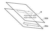
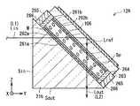
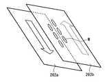
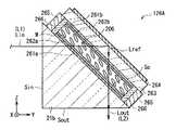
具体的には、図4に示したように、液晶調光素子26は、前述した入射面Sin、出射面Soutおよび載置面Spを有するプリズム21bにおける載置面Sp上に配置(形成)されている。詳細には、液晶調光素子26は、鏡筒部材20とプリズム21b(載置面Sp)との間隙部(間隙領域)20G(隙間,これらの間の空間領域)に配置されている。なお、図中に示したように、鏡筒部材20におけるプリズム21bの背面側(載置面Sp側)には、鏡筒装置2と撮像装置1の本体部10とを取り付ける際に用いられる位置決め孔20H(ボス穴)が、Y軸方向に沿って形成されている。 Specifically, as shown in FIG. 4, the liquid crystal
図5は、液晶調光素子26の詳細な断面構成例(Y−Z断面構成例)を、プリズム21bとともに模式的に表したものである。液晶調光素子26は、プリズム21b側から、透明電極261a、配向膜262a、液晶層260、配向膜262b、透明電極261b、透明基板263(基板)および反射膜264がこの順に配置された積層構造を有している。すなわち、液晶層260の一方の面側にプリズム21bが設けられ、他方の面側に透明基板263および反射膜264がこの順に設けられている。液晶層260(第1液晶層)は仕切り部材267で区切られた液晶層260aおよび液晶層260bにより構成されている。液晶層260a,260bが配置されている領域をそれぞれ配向領域268a,268bとする。液晶調光素子26にはまた、シール剤265、スペーサー266および封止部(図示せず)が設けられている。 FIG. 5 schematically shows a detailed cross-sectional configuration example (YZ cross-sectional configuration example) of the liquid crystal
液晶層260は液晶分子を含有する層であり、ここでは液晶分子に加えて所定の二色性染料分子を含有するようになっている(図5では図示の簡略化のため、液晶分子および二色性染料分子をまとめて「分子Ma,Mb」として示している)。すなわち、液晶調光素子26は、二色性色素を含有するゲスト−ホスト型の液晶を用いて構成されている。 The
本実施の形態では、液晶層260がポジ型およびネガ型のいずれの液晶によって構成されていてもよいが、以下では、液晶層260がネガ型の液晶からなる場合について代表して説明する。一般的に、代表的なネガ型液晶であるVA(Vertical Alignmnt)方式用途の液晶では配向膜にラビング処理を行わないが、本実施の形態では配向膜にラビング処理が施され、液晶分子の配向方向が制御されている。 In the present embodiment, the
液晶層260は、プリズム21bと略同等(好ましくは同一)の光屈折率を有する液晶を用いて構成されているのが望ましい。これにより、プリズム21bと液晶調光素子26(液晶層260)との界面において撮像光が屈折(反射)され、撮像光の光路が光軸L1,L2からずれてしまうのが回避されるからである。なお、液晶調光素子26内の他の部材(透明電極261a,261bや配向膜262a,262b等)の光屈折率による影響については、以下の理由から実質的に考慮しなくてもよい。まず、これらの部材の厚みは、非常に小さい(数十nm〜数百nm程度)ためである。また、配向膜262a,262bの光屈折率は、液晶層260の光屈折率と同程度となるように設定されるのが一般的であり、透明電極261a,261bについては、それらの膜厚の調整によって容易に光屈折率の合わせ込みを行うことができるからである。 The
本実施の形態の液晶層260は前述のように、液晶層260a,260bにより構成されている。この液晶層260a,260bは、それぞれ分子Ma,Mbを含有しており、分子Ma,Mbは同種の液晶分子、二色性染料分子であるが、分子Maと分子Mbとの配向方向(倒れ方向)は互いに異なる。液晶層260a,260bが配置されている領域をそれぞれ配向領域268a,268bとする。 As described above, the
ここで、図6を用いて配向方向の制御方法について説明する。図6(A)に、電圧無印加時の液晶分子Mrと基板263との関係を示し、図6(B)に電圧印加時の液晶分子Mrと基板263との関係を示した。一般的に、液晶分子の長軸方向と基板界面(配向膜)とのなす角度、所謂プレチルト角は、配向膜に対するラビング処理により制御される。このようなラビング処理を行うことにより、図6(A)に示した液晶分子Mrと基板263とが略垂直の状態から、電圧を印加していくと、図6(B)に示したようにラビング処理により決定された方向へと液晶分子Mrが倒れる。 Here, a method of controlling the orientation direction will be described with reference to FIG. FIG. 6A shows the relationship between the liquid crystal molecules Mr and the
上記のように配向膜262a(第1配向膜),262b(第2配向膜)はそれぞれ、液晶層260a,260b内の分子Ma,Mbを所望の方向(配向方向)に配向させるための膜である。これらの配向膜262a,262bはそれぞれ、例えばポリイミド等の高分子材料や無機材料からなる。この配向膜262a,262bに予め所定の方向のラビング処理が施されることによって液晶分子の配向方向が設定されるようになっている。 As described above, the
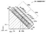
図7は配向膜262a,262bのラビング処理の方向を表した図である。図中の矢印がラビング処理の方向を表す。なお、実線が配向膜262aに対するラビング処理の方向、破線が配向膜262bに対するラビング処理の方向である。後述の図10,図15,図22および図27についても同様とする。図7に示したように、配向膜262a,262bには仕切り部材267を基準として対称となる方向にラビング処理がなされる。すなわち、配向領域268aにおける配向膜262a,262bへのラビング処理の方向と配向領域268bにおける配向膜262a,262bへのラビング処理の方向とが仕切り部材267を基準として対称となっている。プリズム21b側の配向膜262aには、プリズム21bの載置面Spの傾斜方向と平行かつ仕切り部材267に向かう方向へとラビング処理が施され、透明基板263側の配向膜262bには、配向膜262aへのラビング方向から180度回転させた方向、すなわち反平行方向のラビング処理が施される。 FIG. 7 is a diagram showing the direction of rubbing treatment of the
図7に示した方向のラビング処理が行われることにより、分子Ma,Mbは仕切り部材267を基準として互いに対称となるように配向する。つまり、液晶層260a内の分子Maと液晶層260b内の分子Mbとは鏡像の関係となっている。 By performing the rubbing process in the direction shown in FIG. 7, the molecules Ma and Mb are oriented so as to be symmetric with respect to the
仕切り部材267は、配向方向の異なる分子Maと分子Mbとが混在することを防止し、かつ液晶層260a内の各分子Maの動作および液晶層260b内の各分子Mbの動作それぞれを揃える役割を担う。分子Maと分子Mbとが仕切り部材267により隔てられていることにより、電圧を印加した際の液晶調光素子26の応答速度が安定化し、撮像装置1において撮影画内の変化が一様となる。特に動画撮影では、撮影画内の変化が一様となることで撮影画に生じる違和感をなくすことができる。加えて、例えば液晶調光素子26をプロジェクタに適用させた場合には投射される画像の明るさを一様に変化させることができる。 The
仕切り部材267は配向領域268aと配向領域268bとの間に、配向膜262aから配向膜262bに亘り設けられている。具体的には、所定の光軸L1と光軸L1が反射膜264により反射された反射光Lref(後述の図8)とが線対称となるような仮想線を配向膜262a,262bに設け、この仮想線に沿って仕切り部材267が形成される。仕切り部材267はシール剤265と同じ材料、例えばエポキシ接着剤やアクリル接着剤等の接着剤により構成することができる。仕切り部材267は、できるだけ薄いことが好ましく、例えば0.2μm程度である。 The
透明電極261a,261bはそれぞれ、液晶層260に対して電圧(駆動電圧)を印加するための電極であり、例えば酸化インジウムスズ(ITO;Indium Tin Oxide)からなる。なお、これらの透明電極261a,261bと電気的に接続するための配線(図示せず)は、適宜配置すればよい。 Each of the
透明基板263は、透明電極261b、配向膜262bおよび反射膜264を支持すると共に液晶層260を封止するための基板であり、例えばガラス基板からなる。なお、ここでは、透明電極261aおよび配向膜262aを支持すると共に液晶層260を封止するための基板が、プリズム21bにより構成されているが、このプリズム21bの代わりに、プリズム21bと透明電極261aとの間に透明基板を更に設けるようにしてもよい。ただし、プリズム21bがこのように基板の役割を兼ねている場合のほうが、液晶調光素子26の構成部材が少なくて済むため望ましいと言える。 The
反射膜264は、透明基板263の鏡筒部材20側(液晶層260の反対側)に配置されており、詳細は後述するが、撮像光を例えば90度の角度で反射(全反射および一部反射)する機能を有する膜である。このような反射膜264は、例えばアルミニウム(Al)もしくは銀(Ag)、またはそれらの合金等の金属膜等からなる。 The
シール剤265は、液晶層260内の分子Ma,Mbを側面側から封止するための部材であり、例えばエポキシ接着剤やアクリル接着剤等の接着剤からなる。スペーサー266は、液晶層260におけるセルギャップ(厚み)を一定に保持するための部材であり、例えば所定の樹脂材料やガラスからなる。図示しない封止部は、液晶層260内に分子Ma,Mbを封入する際の封入口であると共に、その後液晶層260内の分子Ma,Mbを外部から封止する部分である。 The sealing
[撮像装置1の作用・効果]
(1.撮像動作)
この撮像装置1では、図1に示した操作ボタン14がユーザ(使用者)によって操作されることにより被写体の撮像動作が行われ、撮像画像(撮像データ)が得られる。具体的には、図1〜図3に示したように、撮像光がレンズ部11を介して鏡筒装置2へ入射し、その撮像光の光路が鏡筒装置2内で屈曲された(折り曲げられた)後、撮像素子3へ出射されて検出される。鏡筒装置2内では、詳細には図3に示したように、まず、光軸L1に沿ってレンズ21a(対物レンズ)を介してプリズム21bへ入射した撮像光は、このプリズム21bの反射面(載置面Sp)上の液晶調光素子26内で反射される。この反射光は、レンズ21cを介して光軸L2に沿って出射される。そして、反射光としての撮像光は、第2〜第5レンズ群22〜25をこの順に通過し、鏡筒装置2から出射される。この鏡筒装置2から出射された撮像光は、光学フィルム15を介して撮像素子3へ入射し検出される。このようにして撮像素子3において取得された撮像信号に対して、制御処理部(図示せず)は、所定の信号処理を行う。また、この制御処理部は、取得された撮像信号に基づいて、鏡筒装置2内の液晶調光素子26に対して、前述した所定のフィードバック制御を行う。[Operation and Effect of Imaging Device 1]
(1. Imaging operation)
In this
このとき、液晶調光素子26では、詳細には図8に示したように、プリズム21bの入射面Sinから載置面Sp(液晶層260)に対して斜め、例えば45度の角度で入射した撮像光(入射光Lin)が、このプリズム21bを介して液晶層260a等を通過し、反射膜264において反射(全反射)される。そして、反射された反射光Lrefは、液晶層260b等を通過し、出射光Loutとしてプリズム21bの出射面Soutから出射される。ここでは、反射層264において反射された後、液晶調光素子26を通過し終える前の光を反射光Lrefとする。この際に、液晶層260に対して所定の電圧(駆動電圧)が印加されると、分子Ma,Mbの配向方向(長軸方向)が変化し、それに応じて液晶層260を通過する撮像光の光量も変化する。したがって、このときの駆動電圧を調整することにより、液晶調光素子26全体を通過する撮像光の光量が、(機械的ではなく)電気的に調整可能となる(任意の調光動作が可能となる)。このようにして、鏡筒装置2内で撮像光に対する光量調整(調光)が行われる。 At this time, in the liquid crystal
(2.特徴的部分の作用)
次に、液晶調光素子26の特徴的部分の作用について、比較例(比較例1,2)と比較しつつ詳細に説明する。(2. Action of characteristic parts)
Next, the operation of the characteristic part of the liquid crystal
(比較例1)
図9は、比較例1に係る液晶調光素子126の断面図(Y−Z断面図)を表したものである。液晶層106に仕切り部材267が設けられておらず、液晶層106内の全ての分子Mの配向方向が同一となっている。この点において液晶調光素子126は本実施の形態の液晶調光素子26と異なる。(Comparative Example 1)
FIG. 9 illustrates a cross-sectional view (YZ cross-sectional view) of the liquid crystal
図10に液晶調光素子126における配向膜262a,262bのラビング処理の方向を示す。液晶調光素子26と異なり、比較例1では配向膜262a内,配向膜262内ではそれぞれ同一方向にラビング処理が施されている。配向膜262a,262bにおけるラビング処理はX軸方向に行われている。配向膜262aには、図9の紙面奥から紙面手前方向、配向膜262bには、配向膜262aへのラビング処理の方向から180度回転させた方向(図9の紙面手前から紙面奥方向)にラビング処理がなされている。 FIG. 10 shows the direction of rubbing treatment of the
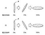
ここで、図11,図12および図13を用いて液晶調光素子126の調光動作について説明する。図11に示したように液晶調光素子126についても、液晶調光素子26と同様に入射光Linが、液晶層106等を通過し、反射層264において反射された反射光Lrefは、再び液晶層106等を通過し、出射光Loutとして出射される。比較例1では、入射光Linと反射光Lrefが通過する液晶層106内の分子Mの配向方向は同じである。 Here, the light control operation of the liquid crystal
図12は入射光Linおよび反射光Lrefの進行方向から見た分子Mの形状を模式的に表したものである。図12(A)は、入射光Linの進行方向から見た分子Mの形状、図12(B)は、反射光Lrefの進行方向から見た分子Mの形状を表す。電圧印加率0%(電圧無印加状態)から電圧無印加率100%(最大電圧印加状態)まで徐々に電圧を印加していくと、分子Mはラビング処理により制御された方向へと倒れていく。このとき、液晶層106内の全ての分子Mの配向方向が同一であるため、分子Mの長軸方向と入射光Linの進行方向とのなす角度,分子Mの長軸方向と反射光Lrefの進行方向とのなす角度が異なるものとなる(例えば、電圧印加率=12%)。 FIG. 12 schematically shows the shape of the molecule M viewed from the traveling direction of the incident light Lin and the reflected light Lref. 12A shows the shape of the molecule M viewed from the traveling direction of the incident light Lin, and FIG. 12B shows the shape of the molecule M viewed from the traveling direction of the reflected light Lref. When a voltage is gradually applied from a voltage application rate of 0% (no voltage applied state) to a voltage no application rate of 100% (maximum voltage applied state), the molecule M falls down in the direction controlled by the rubbing process. . At this time, since the orientation directions of all the molecules M in the
図13は、電圧を印加していった際の比較例1に係る電圧印加率と透過率(光透過率)との関係の一例を示す特性図である。比較例1では、液晶層106にネガ型のゲスト−ホスト型液晶を用い、電圧無印加状態(0V状態)における撮像光の透過光量を基準(100%)として示している。なお、この条件は後述の図18,図20,図25および図29についても同様である。図13より、電圧印加率が大きくなるのに応じて液晶層106での遮光量が急激に大きくなっていき(透過率が急激に低くなっていき)、電圧印加率=50%程度で透過率=50%程度(略一定値)に収束していることが分かる。また、図10に示したラビング処理の方向と逆方向のラビング処理を行っても、図13に示した特性と同様の結果が得られた。 FIG. 13 is a characteristic diagram showing an example of the relationship between the voltage application rate and the transmittance (light transmittance) according to Comparative Example 1 when a voltage is applied. In Comparative Example 1, a negative type guest-host type liquid crystal is used for the
このような液晶調光素子における透過率変化の際の値や傾き、調光範囲はそれぞれ、液晶層の材料や濃度、液晶層のセルギャップ(厚み)、配向膜の種類(材料)等に応じて変化するようになっている。例えば、液晶層106においてポジ型のゲスト−ホスト型液晶を用いた場合には、図13の特性とは逆に、電圧無印加状態(電圧印加率=0%)で透過率が低く、電圧印加率が大きくなるのに応じて透過率が上昇していく傾向となる。 The value, inclination, and dimming range at the time of transmittance change in such a liquid crystal light adjusting device depend on the material and concentration of the liquid crystal layer, the cell gap (thickness) of the liquid crystal layer, the type (material) of the alignment film, etc. Change. For example, when positive type guest-host type liquid crystal is used in the
(比較例2)
図14は、比較例2に係る液晶調光素子126Aの断面図(Y−Z断面図)を表したものである。この比較例2の液晶調光素子126Aでは、比較例1に係る液晶調光素子126と同様に液晶層206に仕切り部材267が設けられておらず、液晶層206内の全ての分子Mの配向方向は同一となっている。比較例2では、比較例1と分子Mの配向方向(配向膜262a,262bのラビング方向)が異なる。(Comparative Example 2)
FIG. 14 illustrates a cross-sectional view (YZ cross-sectional view) of the liquid crystal
図15に液晶調光素子126Aにおける配向膜262a,262bのラビング方向を示した。比較例1と同様に配向膜262a内,配向膜262b内ではそれぞれ同一方向にラビング処理が施される。ラビング処理はプリズム21bの載置面Spの傾斜方向と平行方向になされ、配向膜262aでは、載置面Spの傾斜を下る方向、配向膜262bでは、配向膜262aへのラビング方向から180度回転させた方向(載置面Spの傾斜を上る方向)に行われる。 FIG. 15 shows the rubbing direction of the
ここで、図16,図17および図18を用いて液晶調光素子126Aの調光動作について説明する。図16に示したように液晶調光素子126Aについても、入射光Linが、液晶層206を通過し、反射層264において反射された反射光Lrefは、再び液晶層206等を通過し、出射光Loutとして出射される。比較例2においても、比較例1と同様に入射光Linと反射光Lrefが通過する液晶層206内の分子Mの配向方向は同じである。 Here, the dimming operation of the liquid
図17は入射光Linおよび反射光Lrefの進行方向から見た分子Mの形状を模式的に表したものである。図17(A)は、入射光Linの進行方向から見た分子Mの形状、図17(B)は、反射光Lrefの進行方向から見た分子Mの形状を表す。比較例1と同様に液晶層260内の全ての分子Mの配向方向が同一であるため、分子Mの長軸方向と入射光Linの進行方向とのなす角度,分子Mの長軸方向と反射光Lrefの進行方向とのなす角度が異なるものとなる(例えば、電圧印加率=15%)。 FIG. 17 schematically shows the shape of the molecule M viewed from the traveling direction of the incident light Lin and the reflected light Lref. FIG. 17A shows the shape of the molecule M viewed from the traveling direction of the incident light Lin, and FIG. 17B shows the shape of the molecule M viewed from the traveling direction of the reflected light Lref. Since the orientation directions of all the molecules M in the
図18に電圧を印加していった際の液晶調光素子126Aにおける電圧印加率と透過率との関係を表す。比較例2では電圧印加率=40%程度で透過率=45%程度(略一定値)まで減光した。図18では、比較例1(図13)と異なり、電圧印加率の増加と共に継続的に透過率の減少が進まず、電圧印加率=15%程度で透過率が一旦上昇している(透過率=110%程度)。これは、電圧印加率15%程度のとき、反射光Lrefの進行方向と分子Mの長軸方向とが平行に近い状態となるためである(図17(B))。また、図17に示したラビング処理の方向と逆方向のラビング処理を行っても、図18に示した特性と同様の結果が得られた。 FIG. 18 shows the relationship between the voltage application rate and the transmittance in the liquid crystal
(本実施の形態の作用)
上記のような比較例1,2と異なり、図8に示したように本実施の形態の液晶調光素子26では、入射光Linは配向領域268aを通過し、反射光Lrefは配向領域268aとは液晶分子の配向方向が異なる配向領域268bを通過する。(Operation of this embodiment)
Unlike the comparative examples 1 and 2 as described above, in the liquid crystal
図19は、本実施の形態の液晶調光素子26において入射光Linおよび反射光Lrefの進行方向から見た分子Ma,Mbの形状を模式的に表したものである。図19(A)は、入射光Linの進行方向から見た分子Maの形状、図19(B)は、反射光Lrefの進行方向から見た分子Mbの形状を表す。徐々に電圧を印加していくと、分子Ma,Mb共に電圧印加率15%程度で入射光Lin,反射光Lrefの進行方向に対して、その長軸方向がほぼ垂直となる。本実施の形態に係る液晶調光素子26では、入射光Linと反射光Lrefとが配向領域268a,268bをそれぞれ通過することにより、分子Maの長軸方向と入射光Linの進行方向とのなす角度,分子Mbの長軸方向と反射光Lrefの進行方向とのなす角度の両方が制御される。 FIG. 19 schematically shows the shapes of the molecules Ma and Mb viewed from the traveling direction of the incident light Lin and the reflected light Lref in the liquid crystal
特に、液晶調光素子26では、仕切り部材267を基準として分子Maの配向方向と分子Mbの配向方向とが対称となるようにしたので、分子Maの長軸方向と入射光Linの進行方向とのなす角度と、分子Mbの長軸方向と反射光Lrefの進行方向とのなす角度とがほぼ等しくなる。 In particular, in the liquid crystal
図20は、電圧を印加していった際の液晶調光素子26における電圧印加率と透過率(光透過率)との関係の一例を表したものである。本実施の形態では、電圧印加率=40%程度で透過率=40%程度(略一定値)に収束していることが分かる。すなわち、液晶調光素子26における調光範囲は、約60%(透過率=100%〜40%の範囲)となっている。 FIG. 20 shows an example of the relationship between the voltage application rate and the transmittance (light transmittance) in the liquid crystal
比較例1(透過率50%)および比較例2(透過率55%)と比較して本実施の形態に係る実施例では、透過率が40%程度まで下がり、調光範囲を60%程度にまで拡大していることがわかる。 Compared with Comparative Example 1 (Transmittance 50%) and Comparative Example 2 (Transmittance 55%), in the example according to the present embodiment, the transmittance is reduced to about 40% and the dimming range is set to about 60%. It can be seen that it has expanded to.
以上のように本実施の形態の液晶調光素子26では、液晶層260の他方の面側に反射膜264を設け、液晶層260が分子Ma,Mbの配向方向が異なる配向領域268a,268bを有するようにしたため、入射光Linと反射光Lrefとが、分子Ma,Mbの配向方向が異なる配向領域268a,268bをそれぞれ通過する(図8)。これにより、分子Maの長軸方向と入射光Linの進行方向とのなす角度,分子Mbの長軸方向と反射光Lrefの進行方向とのなす角度を共に制御することができる。よって、液晶調光素子26の調光範囲を拡大することができる。 As described above, in the liquid crystal
また、本実施の形態では、隣接する配向領域268a,268bの分子Ma,Mbの配向方向を配向領域268a,268bの境界(仕切り部材267)を基準として対称とすることにより、入射光Linの進行方向と分子Maの長軸方向とのなす角度,反射光Lrefの進行方向と分子Mbの長軸方向とのなす角度がほぼ等しくなる。よって、より効果的に調光範囲が拡大される。 In the present embodiment, the alignment direction of the molecules Ma and Mb of the
なお、液晶調光素子26は2つの配向領域268a,268bにより構成されているが、液晶調光素子が3つ以上の配向領域により構成されていてもよい。このとき、それぞれの配向領域における液晶分子の配向方向は全て異なっていてもよく、また、同じ配向方向の配向領域が存在していてもよい。 In addition, although the liquid-crystal
<変形例>
続いて、上記第1の実施の形態の変形例について説明する。なお、上記実施の形態における構成要素と同一のものには同一の符号を付し、適宜説明を省略する。<Modification>
Next, a modification of the first embodiment will be described. In addition, the same code | symbol is attached | subjected to the same thing as the component in the said embodiment, and description is abbreviate | omitted suitably.
図21は、変形例に係る液晶調光素子26Aの断面構成例(Y−Z断面構成例)を、プリズム21bとともに模式的に表したものである。この液晶調光素子26Aでは、上記実施の形態の液晶調光素子26と分子Ma,Mbの配向方向(配向膜262a,262bへのラビング処理の方向)が逆となっている。 FIG. 21 schematically illustrates a cross-sectional configuration example (YZ cross-sectional configuration example) of the liquid crystal
図22は配向膜262a,262bにおけるラビング処理の方向を表したものである。配向膜262a,262bには仕切り部材267を基準として対称となる方向のラビング処理がなされる。本変形例では、上記実施の形態の液晶調光素子26と逆方向にラビング処理が行われる。詳細には、透明基板263側の配向膜262bには、プリズム21bの載置面Spの傾斜方向と平行かつ仕切り部材267に向かう方向へとラビング処理が施され、プリズム21b側の配向膜262aには、配向膜262bへのラビング方向から180度回転させた方向、すなわち反平行方向のラビング処理が施される。 FIG. 22 shows the direction of rubbing treatment in the
図22に示した方向のラビング処理が行われることにより、分子Maおよび分子Mbは仕切り部材267を基準として互いに対称となるように配向する。つまり、液晶層260a内の分子Maと液晶層260b内の分子Mbとは鏡像の関係となっている。 By performing the rubbing process in the direction shown in FIG. 22, the molecules Ma and Mb are oriented so as to be symmetrical with respect to the
本変形例の液晶調光素子26Aにおいても、液晶調光素子26と同様の調光動作を行うことが可能である。すなわち、図23に示したように、プリズム21bの入射面Sinから入射した撮像光(入射光Lin)が、このプリズム21bを介して液晶層260a等を通過し、反射層264において反射される。そして、反射された反射光Lrefは、液晶層260b等を通過し、出射光Loutとしてプリズム21bの出射面Soutから出射される。液晶調光素子26Aでは、入射光Linは配向領域268aを通過し、反射光Lrefは配向領域268aとは液晶分子の配向方向が異なる配向領域268bを通過する。 Also in the liquid crystal
図24は入射光Linおよび反射光Lrefの進行方向から見た分子Ma,Mbの形状を模式的に表したものである。図24(a)は、入射光Linの進行方向から見た分子Maの形状、図24(b)は、反射光Lrefの進行方向から見た分子Mbの形状を表す。徐々に電圧を印加していくと、分子Ma,Mb共に電圧印加率15%程度で入射光Lin,反射光Lrefに対して、その長軸方向がほぼ平行となる。すなわち、電圧印加率15%では入射光Lin,出射光Loutを透過しやすい方向に分子Ma,Mbが配向する。 FIG. 24 schematically shows the shapes of the molecules Ma and Mb viewed from the traveling direction of the incident light Lin and the reflected light Lref. 24A shows the shape of the molecule Ma seen from the traveling direction of the incident light Lin, and FIG. 24B shows the shape of the molecule Mb seen from the traveling direction of the reflected light Lref. When a voltage is gradually applied, the major axis direction of the molecules Ma and Mb becomes substantially parallel to the incident light Lin and the reflected light Lref at a voltage application rate of about 15%. That is, when the voltage application rate is 15%, the molecules Ma and Mb are oriented in a direction in which the incident light Lin and the outgoing light Lout are easily transmitted.
図25は、この液晶調光素子26Aでの電圧印加率と透過率との関係の一例を表したものである。本変形例では、図20と異なり、電圧印加率15%程度で透過率が一旦急激に上昇する。これは前述のように分子Ma,Mbが入射光Lin,出射光Loutを透過しやすい方向に配向するためである。一度このような透過率のピークをむかえた後は、電圧印加率の増加に伴い、透過率は減少していき、電圧印加率=50%程度で透過率=50%程度(略一定値)に収束している。 FIG. 25 shows an example of the relationship between the voltage application rate and the transmittance in the liquid crystal
図25より、本変形例では透過率50%程度までしか遮光できないため、上記実施の形態と比較して調光範囲が狭いとも思える。しかし、電圧印加率15%では電圧無印加の状態よりも透過率が上昇し、その透過率は160%程度となっている。よって、このピークを考慮すると調光範囲は110%(透過率=160%〜50%の範囲)となる。 From FIG. 25, it can be considered that the light control range is narrower than that of the above-described embodiment because the present modification can shield light only up to about 50% transmittance. However, when the voltage application rate is 15%, the transmittance is higher than when no voltage is applied, and the transmittance is about 160%. Therefore, in consideration of this peak, the light control range is 110% (transmittance = 160% to 50% range).
このように幅広い調光範囲を実現可能な液晶調光素子26Aは、撮像装置等の分野において有用である。しかし一方で、このように電圧を印加していく際に透過率が一旦上昇するものは、その後の透過率の減少が急峻であるため使用できる電圧範囲が限定される。よって、特性を考慮し、液晶調光素子を適用する状況に応じて液晶調光素子26あるいは液晶調光素子26Aを使い分けることが望ましい。 Thus, the liquid crystal
[第2の実施の形態]
次に、第2の実施の形態について説明する。なお、上記第1の実施の形態における構成要素と同一のものには同一の符号を付し、適宜説明を省略する。[Second Embodiment]
Next, a second embodiment will be described. In addition, the same code | symbol is attached | subjected to the same component as the said 1st Embodiment, and description is abbreviate | omitted suitably.
図26は、第2の実施の形態に係る液晶調光素子27の断面構成例(Y−Z断面構成例)を、プリズム21bとともに模式的に表したものである。この液晶調光素子27では、液晶層が1層(単層)構造(液晶層260)であった上記第1の実施の形態の液晶調光素子26とは異なり、液晶層が2層(複数層)構造となっている。すなわち、液晶調光素子27では、以下詳述するように、2層の液晶層260,260cが積層されてなる。 FIG. 26 schematically illustrates a cross-sectional configuration example (YZ cross-sectional configuration example) of the liquid crystal
具体的には、液晶調光素子27は、プリズム21b側から、透明電極261a、配向膜262a、液晶層260、配向膜262b、透明電極261b、透明基板263、透明電極261a、配向膜262c、液晶層260c(第2液晶層)、配向膜262d、透明電極261b、透明基板263および反射膜264がこの順に積層された積層構造を有している。この液晶調光素子27では、液晶調光素子26と同様に、配向領域268a,268bを有し、液晶層260が仕切り部材267で区切られた液晶層260aおよび液晶層260bにより構成されている。液晶層260,260cの側面側にそれぞれシール剤265、スペーサー266および封止部(図示せず)が設けられている。 Specifically, the liquid crystal
液晶層260,260cはそれぞれ、液晶調光素子26と同様に、二色性色素を含有するゲスト−ホスト型液晶を用いて構成されている。具体的には、液晶層260を構成する液晶層260a,260bは、それぞれ分子Ma,Mbを含有し、液晶層260cは、分子Mc(液晶分子および二色性色素分子)を含有している。また、上記第1の実施の形態と同様に分子Ma,Mbの配向方向は互いに異なる。なお、ここでは液晶層260cは全ての分子Mcの配向方向が同一となっているが、液晶層260と同様に液晶分子の配向方向が異なる複数の配向領域の液晶層により構成されていてもよい。 Each of the liquid crystal layers 260 and 260 c is configured by using a guest-host type liquid crystal containing a dichroic dye, like the liquid crystal
図27は配向膜262a,262b,262c,262dのラビング方向を表したものである。図27に示したように、配向膜262a,262bに対しては、仕切り部材267を基準として対称となる方向のラビング処理がなされる。ラビング方向は上記第1の実施の形態と同じである(図7)。配向膜262c,262dには、配向膜262a,262bになされたラビング処理の方向と直交する方向のラビング処理がなされる。詳細には、配向膜262cに、図26の紙面奥から紙面手前方向、配向膜262dに、配向膜262cのラビング方向から180度回転させた方向(図26の紙面手前から紙面奥方向)のラビング処理が行われる。 FIG. 27 shows the rubbing direction of the
図27に示した方向のラビング処理を行うことにより、分子Ma,Mbは仕切り部材267を基準として互いに対称となるように配向する。つまり、液晶層260a内の分子Maと液晶層260b内の分子Mbとは鏡像の関係となっている。分子Mcは分子Ma,Mbと直交する方向に配向する。 By performing the rubbing process in the direction shown in FIG. 27, the molecules Ma and Mb are oriented so as to be symmetrical with respect to the
本実施の形態の液晶調光素子27においても、液晶調光素子26と同様の調光動作を行うことが可能である。すなわち、図28に示したように、プリズム21bの入射面Sinから入射した撮像光(入射光Lin)が、このプリズム21bを介して液晶層260a,260c等を通過し、反射層264において反射される。そして、反射された反射光Lrefは、液晶層260c,260b等を通過し、出射光Loutとしてプリズム21bの出射面Soutから出射される。なお、液晶層260,260cに対する駆動電圧(印加電圧)が互いに異なるようにした場合には、例えば、撮像光における特定方向の偏光(偏光成分)を意図的に弱めつつ、一定の光量を保持するといったことも可能となる。 Also in the liquid crystal
ただし、この液晶調光素子27は、上記したように、2層の液晶層260,260cが積層されてなることにより、以下の効果も得られる。すなわち、まず、一般にゲスト−ホスト型液晶では、ホストとしての液晶に溶ける色素の種類や溶解量には限界があるため、液晶調光素子における調光範囲もある程度限られたものとなることが知られている。ここで、ある一定濃度のゲスト−ホスト型液晶を用いた場合、液晶層のセルギャップを増加させる(厚みを大きくする)ことによって調光範囲を増加させることが可能であるものの、セルギャップの増大は液晶の応答速度に悪影響を及ぼしてしまう(液晶の応答速度が低下してしまう)。そこで、調光範囲を増加させるために偏光板を併用することが考えられるが、偏光板が固定(偏光軸が固定)されてしまうと、この液晶調光素子を撮像装置に適用させた場合、撮像装置におけるレンズのF値が低下してしまう。そのため、偏光板を光路に対して出し入れ可能(挿脱自体)に構成して用いることが現実的であるが、そのような構成の偏光板を併用した場合、鏡筒装置(ひいては撮像装置)の省スペース化(薄型化)を図ることが困難となってしまう。 However, as described above, the liquid crystal
これに対して本変形例の液晶調光素子27では、上記した2層構造の液晶層260,260cからなることにより、液晶層自体のセルギャップ(厚み)はそのままで(変化させることなく)、液晶の応答速度も保持しつつ(低下させることなく)、調光範囲を増加させることが可能となる。 On the other hand, in the liquid crystal
図29は、上記第1の実施の形態における図20と同様に、液晶調光素子27における電圧印加率と透過率との関係を示す一実施例を表したものである。この図29から、本実施の形態では、電圧印加率=40%程度で透過率=20%以下(略一定値)に収束していることが分かる。すなわち、この実施例では、液晶調光素子27における調光範囲が約80%(透過率=100%〜20%の範囲)となっており、図20に示した液晶調光素子26の実施例と比べ、更に調光範囲が拡大していることが分かる。 FIG. 29 shows an example showing the relationship between the voltage application rate and the transmittance in the liquid crystal
以上のように第2の実施の形態に係る液晶調光素子27では、液晶分子の配向方向が異なる配向領域268a,268bを設けたことに加え、液晶層を液晶層260,260cから構成される2層構造としたことで、液晶調光素子27の調光範囲を更に拡大することが可能となる。 As described above, in the liquid crystal
なお、本実施の形態では液晶層が2層構造となっている場合について説明したが、この場合には限られず、液晶調光素子内において液晶層が3層以上の積層構造となっているようにしてもよい。 Note that although the case where the liquid crystal layer has a two-layer structure has been described in this embodiment mode, the present invention is not limited to this case, and the liquid crystal layer has a laminated structure of three or more layers in the liquid crystal light control device. It may be.
また、配向膜262a,262b,262c,262dへのラビング処理の方向は限定されるものではないが、液晶層260の配向方向を制御する配向膜262a,262bへのラビング処理の方向と液晶層260cの配向方向を制御する配向膜262c,262dへのラビング処理の方向とが直交するとき、特に調光範囲を拡大することができる。ここでは、配向膜262a,262bに対して、上記第1の実施の形態に係る液晶調光素子26と同方向のラビング処理を行ったが、配向膜262a,262bに上記変形例に係る液晶調光素子26Aと同方向のラビング処理を行ってもよい。 The direction of the rubbing process for the
[その他の変形例]
以上、実施の形態および変形例を挙げて本発明を説明したが、本発明はこれらの実施の形態等に限定されず、種々の変形が可能である。[Other variations]
While the present invention has been described with reference to the embodiments and modifications, the present invention is not limited to these embodiments and the like, and various modifications can be made.
例えば上記実施の形態等では、ラビング処理の方向をプリズム21bの載置面Spの傾斜方向と平行または垂直方向としたが、傾斜方向に対して斜めにラビング処理を行ってもよい。また、上記実施の形態等では、対向する配向膜には反平行方向のラビング処理を行ったが、対向する配向膜に同方向のラビング処理を行ってもよく、あるいは図30に示したように一方の配向膜に、他方の配向膜から90度(270度)回転させた方向のラビング処理を行ってもよい。更に、液晶分子の配向方向を制御するため、ホスト液晶に添加物を加え、液晶分子の回転角を調整してもよい。 For example, in the above-described embodiment, the rubbing process is performed in a direction parallel or perpendicular to the inclination direction of the mounting surface Sp of the
上記のように液晶分子の配向方向(ラビング処理の方向)の組み合わせを設計する際には、例えば、まず全ての液晶分子の配向方向が同一の液晶セル(基板,透明電極,配向膜および液晶層)を用いて検討を行う。図31に示したようにこの液晶セル306の基板に対して液晶調光素子への入射角に相当する角度θ、例えば45度の方向から光を液晶セル306へと入射させ、電圧印加率による液晶セル306の透過率変化を測定する。このような検討を重ねることにより所望の調光範囲が得られる液晶分子の配向方向を設計する。 When designing a combination of alignment directions of liquid crystal molecules (rubbing direction) as described above, for example, first, a liquid crystal cell (substrate, transparent electrode, alignment film, and liquid crystal layer) in which the alignment directions of all liquid crystal molecules are the same. ). As shown in FIG. 31, light is incident on the liquid crystal cell 306 from the direction of an angle θ corresponding to the incident angle to the liquid crystal light control device, for example, 45 degrees, with respect to the substrate of the liquid crystal cell 306, and the voltage application rate is determined. A change in transmittance of the liquid crystal cell 306 is measured. By repeating such studies, the orientation direction of liquid crystal molecules that can obtain a desired light control range is designed.
また、例えば、上記実施の形態等では、ゲスト−ホスト型の液晶を用いた液晶調光素子を例に挙げて説明したが、この場合には限られず、ゲスト−ホスト型の液晶以外の液晶を用いた液晶調光素子を用いるようにしてもよい。 Further, for example, in the above-described embodiment and the like, a liquid crystal light control element using a guest-host type liquid crystal has been described as an example. However, the present invention is not limited to this, and a liquid crystal other than the guest-host type liquid crystal is used. You may make it use the used liquid crystal light control element.
更に、上記実施の形態等では、鏡筒装置内の屈曲領域にプリズムが配置されている場合について説明したが、場合によっては、プリズム以外の光学部材(例えば、ミラーなど)が鏡筒装置内の屈曲領域に配設されているようにしてもよい。 Further, in the above-described embodiment, etc., the case where the prism is arranged in the bending region in the lens barrel device has been described. However, in some cases, an optical member other than the prism (for example, a mirror or the like) is provided in the lens barrel device. It may be arranged in the bent region.
加えて、上記実施の形態等では、鏡筒装置や撮像装置等の各構成要素(光学系)を具体的に挙げて説明したが、全ての構成要素を備える必要はなく、また、他の構成要素を更に備えていてもよい。なお、上記実施の形態等においては、撮像装置としてデジタルスチルカメラを例示したが、本発明はビデオカメラやテレビカメラなどの撮像装置やライトバルブ、反射型表示体あるいは光スイッチ素子など調光素子を有する種々の装置に適用可能である。 In addition, in the above-described embodiment and the like, each component (optical system) such as the lens barrel device and the imaging device has been specifically described, but it is not necessary to include all the components, and other configurations An element may be further provided. In the above-described embodiments and the like, a digital still camera is exemplified as the imaging device. However, the present invention includes an imaging device such as a video camera or a television camera, a light valve, a reflective display body, or a light control element such as an optical switch element. The present invention can be applied to various devices.
1…撮像装置、10…本体部、11…レンズ部、2…鏡筒装置、20…鏡筒部材、20G…間隙部、20H…位置決め孔(ボス穴)、21…第1レンズ群、21b…プリズム、22…第2レンズ群、23…第3レンズ群、24…第4レンズ群、25…第5レンズ群、26,26A,27…液晶調光素子、260,260a,260b,260c…液晶層、261a,261b…透明電極、262a,262b,262c,262d…配向膜、263…透明基板、264…反射膜、265…シール材、266…スペーサー、267…仕切り、268a,268b…配向領域、3…撮像素子、L1,L2…光軸、Lin…入射光、Lout…出射光、Lref…反射光、Sin…入射面、Sout…出射面、Sp…載置面(反射面)、M,Ma,Mb,Mc…分子(液晶分子・色素分子)。 DESCRIPTION OF
Claims (12)
Translated fromJapanese前記第1液晶層を透過する光を反射する反射膜とを備え、
前記第1液晶層は隣接する配向領域を有し、前記隣接する配向領域間の液晶分子の配向
方向が異なっている
液晶調光素子。A first liquid crystal layer on which light is incident from one surface;
A reflective film that reflects light transmitted through the first liquid crystal layer;
The first liquid crystal layer has adjacent alignment regions, and the alignment directions of liquid crystal molecules between the adjacent alignment regions are different.
基準として対称となっている
請求項1記載の液晶調光素子。The liquid crystal light control device according to claim 1, wherein in the adjacent alignment region, the alignment direction of the liquid crystal molecules is symmetrical with respect to a boundary between the adjacent alignment regions.
が設けられ、
前記第1配向膜は、前記隣接する配向領域に対応する領域に異なる方向のラビング処理が施されている
請求項1または2記載の液晶調光素子。A first alignment film and a second alignment film are provided on one surface and the other surface of the first liquid crystal layer,
The liquid crystal light control device according to claim 1, wherein the first alignment film is subjected to a rubbing process in a different direction in a region corresponding to the adjacent alignment region.
請求項3記載の液晶調光素子。The liquid crystal light control device according to claim 3, wherein a direction of rubbing treatment applied to the first alignment film is symmetric with respect to a boundary between the adjacent alignment regions and a direction toward the boundary.
請求項4記載の液晶調光素子。The liquid crystal light control device according to claim 4, wherein a direction of rubbing treatment applied to the second alignment film is antiparallel to a direction of rubbing treatment of the first alignment film.
側にプリズムを有する
請求項1または2記載の液晶調光素子。The liquid crystal light control device according to claim 1, further comprising a substrate between the first liquid crystal layer and the reflective film, and a prism on one surface side of the first liquid crystal layer.
請求項1または2記載の液晶調光素子。The liquid crystal light control device according to claim 1, further comprising a second liquid crystal layer between the first liquid crystal layer and the reflective film.
請求項7記載の液晶調光素子。The liquid crystal light control device according to claim 7, wherein in the second liquid crystal layer, alignment directions of liquid crystal molecules are aligned in one direction.
請求項1または2記載の液晶調光素子。The liquid crystal light control device according to claim 1, further comprising a partition member at a boundary between the adjacent alignment regions.
請求項1または2記載の液晶調光素子。The liquid crystal light control device according to claim 1, wherein the first liquid crystal layer is configured using a guest-host (GH) type liquid crystal containing a dichroic dye.
請求項1または2記載の液晶調光素子。The alignment direction of the alignment region passing therethrough is at least partially different between the light incident on the first liquid crystal layer from the one surface and the light reflected by the reflective film and emitted to the one surface. Item 3. A liquid crystal light control device according to item 1 or 2.
前記液晶調光素子は、
一方の面から光が入射する第1液晶層と、
前記第1液晶層を透過する光を反射する反射膜とを備え、
前記第1液晶層は隣接する配向領域を有し、前記隣接する配向領域間の液晶分子の配向
方向が異なっている
撮像装置。A liquid crystal light control device and an image sensor;
The liquid crystal light control device is
A first liquid crystal layer on which light is incident from one surface;
A reflective film that reflects light transmitted through the first liquid crystal layer;
The first liquid crystal layer has adjacent alignment regions, and the alignment directions of liquid crystal molecules between the adjacent alignment regions are different.
Priority Applications (3)
| Application Number | Priority Date | Filing Date | Title |
|---|---|---|---|
| JP2010243257AJP5682232B2 (en) | 2010-10-29 | 2010-10-29 | Liquid crystal light control device and imaging apparatus |
| US13/137,895US8743297B2 (en) | 2010-10-29 | 2011-09-21 | Liquid crystal light adjusting device and imaging apparatus |
| CN2011103225732ACN102466903A (en) | 2010-10-29 | 2011-10-21 | Liquid crystal light adjusting device and imaging apparatus |
Applications Claiming Priority (1)
| Application Number | Priority Date | Filing Date | Title |
|---|---|---|---|
| JP2010243257AJP5682232B2 (en) | 2010-10-29 | 2010-10-29 | Liquid crystal light control device and imaging apparatus |
Publications (2)
| Publication Number | Publication Date |
|---|---|
| JP2012098321Atrue JP2012098321A (en) | 2012-05-24 |
| JP5682232B2 JP5682232B2 (en) | 2015-03-11 |
Family
ID=45996338
Family Applications (1)
| Application Number | Title | Priority Date | Filing Date |
|---|---|---|---|
| JP2010243257AExpired - Fee RelatedJP5682232B2 (en) | 2010-10-29 | 2010-10-29 | Liquid crystal light control device and imaging apparatus |
Country Status (3)
| Country | Link |
|---|---|
| US (1) | US8743297B2 (en) |
| JP (1) | JP5682232B2 (en) |
| CN (1) | CN102466903A (en) |
Families Citing this family (5)
| Publication number | Priority date | Publication date | Assignee | Title |
|---|---|---|---|---|
| CN104181640B (en)* | 2014-08-25 | 2017-02-08 | 华中科技大学 | Optical switching module based on liquid crystal variable-focus lens |
| KR102513511B1 (en)* | 2016-04-28 | 2023-03-22 | 엘지디스플레이 주식회사 | Liquid Crystal Display Device And Method Of Fabricating The Same |
| CN106855675B (en)* | 2017-03-14 | 2020-01-07 | 京东方科技集团股份有限公司 | Anti-peep devices and anti-peep display devices |
| CN115775490A (en)* | 2021-09-07 | 2023-03-10 | 张家港莱拓新材料科技有限公司 | LCP peep-proof film layer structure and peep-proof display device with same |
| JP2025138285A (en)* | 2024-03-11 | 2025-09-25 | 株式会社ジャパンディスプレイ | Liquid crystal panel, imaging module and imaging device |
Citations (8)
| Publication number | Priority date | Publication date | Assignee | Title |
|---|---|---|---|---|
| JPS61232420A (en)* | 1985-04-08 | 1986-10-16 | Matsushita Electric Ind Co Ltd | Transmissive liquid crystal display device |
| JPH07333432A (en)* | 1994-06-07 | 1995-12-22 | Matsushita Electric Ind Co Ltd | Optical functional element and liquid crystal display device |
| JPH09305092A (en)* | 1996-05-10 | 1997-11-28 | Fuji Xerox Co Ltd | Light control element and its manufacture |
| JPH1068943A (en)* | 1996-05-17 | 1998-03-10 | Motorola Inc | Nematic liquid crystal phase spatial light modulator with high display resolution |
| JP2000314888A (en)* | 1999-04-30 | 2000-11-14 | Seiko Epson Corp | Liquid crystal panel, method of manufacturing the same, and projection display device |
| JP2003029302A (en)* | 2001-07-18 | 2003-01-29 | Sony Corp | Dimmer and image pickup device |
| JP2006292990A (en)* | 2005-04-11 | 2006-10-26 | Konica Minolta Photo Imaging Inc | Shutter unit and optical unit and imaging apparatus using the shutter unit |
| JP2007505338A (en)* | 2003-09-09 | 2007-03-08 | コニンクリユケ フィリップス エレクトロニクス エヌ.ブイ. | Mirror with built-in display |
Family Cites Families (11)
| Publication number | Priority date | Publication date | Assignee | Title |
|---|---|---|---|---|
| JP2001186401A (en)* | 1999-12-24 | 2001-07-06 | Minolta Co Ltd | Digital camera |
| WO2001061383A1 (en)* | 2000-02-16 | 2001-08-23 | Matsushita Electric Industrial Co., Ltd. | Irregular-shape body, reflection sheet and reflection-type liquid crystal display element , and production method and production device therefor |
| JP3791377B2 (en)* | 2001-09-28 | 2006-06-28 | 株式会社日立製作所 | Liquid crystal display element and display device using the same |
| JP3917417B2 (en)* | 2001-12-11 | 2007-05-23 | シャープ株式会社 | Reflective liquid crystal display |
| KR100845410B1 (en)* | 2003-05-14 | 2008-07-10 | 엘지디스플레이 주식회사 | Multi Domain Alignment Film Formation Method |
| KR101035844B1 (en)* | 2004-01-06 | 2011-05-19 | 삼성전자주식회사 | Upper substrate and liquid crystal display device having the same |
| CN100576035C (en)* | 2004-05-21 | 2009-12-30 | 三洋电机株式会社 | Semi-transmissive liquid crystal display device and color liquid crystal display device |
| US7573551B2 (en)* | 2004-05-21 | 2009-08-11 | Sanyo Electric Co., Ltd. | Transflective liquid crystal display device and color liquid crystal display device |
| GB2427033A (en)* | 2005-06-07 | 2006-12-13 | Sharp Kk | A display switchable between public and private modes |
| JP2008177070A (en)* | 2007-01-19 | 2008-07-31 | Sony Corp | Optical control element, planar light source device, and liquid crystal display device |
| KR101632925B1 (en)* | 2009-09-21 | 2016-07-04 | 삼성디스플레이 주식회사 | Display apparatus and method of manufacturing the same |
- 2010
- 2010-10-29JPJP2010243257Apatent/JP5682232B2/ennot_activeExpired - Fee Related
- 2011
- 2011-09-21USUS13/137,895patent/US8743297B2/ennot_activeExpired - Fee Related
- 2011-10-21CNCN2011103225732Apatent/CN102466903A/enactivePending
Patent Citations (8)
| Publication number | Priority date | Publication date | Assignee | Title |
|---|---|---|---|---|
| JPS61232420A (en)* | 1985-04-08 | 1986-10-16 | Matsushita Electric Ind Co Ltd | Transmissive liquid crystal display device |
| JPH07333432A (en)* | 1994-06-07 | 1995-12-22 | Matsushita Electric Ind Co Ltd | Optical functional element and liquid crystal display device |
| JPH09305092A (en)* | 1996-05-10 | 1997-11-28 | Fuji Xerox Co Ltd | Light control element and its manufacture |
| JPH1068943A (en)* | 1996-05-17 | 1998-03-10 | Motorola Inc | Nematic liquid crystal phase spatial light modulator with high display resolution |
| JP2000314888A (en)* | 1999-04-30 | 2000-11-14 | Seiko Epson Corp | Liquid crystal panel, method of manufacturing the same, and projection display device |
| JP2003029302A (en)* | 2001-07-18 | 2003-01-29 | Sony Corp | Dimmer and image pickup device |
| JP2007505338A (en)* | 2003-09-09 | 2007-03-08 | コニンクリユケ フィリップス エレクトロニクス エヌ.ブイ. | Mirror with built-in display |
| JP2006292990A (en)* | 2005-04-11 | 2006-10-26 | Konica Minolta Photo Imaging Inc | Shutter unit and optical unit and imaging apparatus using the shutter unit |
Also Published As
| Publication number | Publication date |
|---|---|
| JP5682232B2 (en) | 2015-03-11 |
| US8743297B2 (en) | 2014-06-03 |
| US20120105743A1 (en) | 2012-05-03 |
| CN102466903A (en) | 2012-05-23 |
Similar Documents
| Publication | Publication Date | Title |
|---|---|---|
| JP5732974B2 (en) | Optical apparatus and imaging apparatus | |
| KR101506587B1 (en) | Method and apparatus for auto-focus using liquid crystal adaptive optics | |
| WO2020125304A1 (en) | Imaging method, imaging device, electronic device, and medium | |
| WO2020114067A1 (en) | Imaging method, imaging device, electronic device, and medium | |
| JP5533780B2 (en) | Liquid crystal lens structure and driving method thereof | |
| US11215809B2 (en) | Periscope-type zooming camera module | |
| WO2012056978A1 (en) | Image pickup device | |
| US20070115211A1 (en) | Liquid crystal shutter device for a camera | |
| JP5682232B2 (en) | Liquid crystal light control device and imaging apparatus | |
| WO2020134779A1 (en) | Imaging method, imaging device, electronic apparatus, and medium | |
| KR20100098724A (en) | Device and method for reducing optical blurring | |
| CN110266851A (en) | Camera module, electronic device, and camera module control method | |
| JP2008090259A (en) | Imaging lens device | |
| JP4033148B2 (en) | Lens barrel and imaging device | |
| US11714333B2 (en) | Optical imaging apparatus capable of focusing | |
| JPH06148730A (en) | Camera shaking correction device | |
| JP4947946B2 (en) | Imaging device | |
| CN118042259B (en) | Camera module, electronic device, shooting method and computer readable storage medium | |
| JP2006317695A (en) | Optical device | |
| JP2016029424A (en) | Image pickup apparatus having polarizing filter | |
| CN218183377U (en) | Anti-shock system for handheld devices | |
| CN111176049A (en) | Liquid crystal optical device, imaging apparatus and imaging method | |
| JP2005257839A (en) | Electrical dimmer element, lens barrel, and imaging device | |
| JP2008541157A (en) | Electro-optic filter | |
| TWM634197U (en) | Image stabilization system for handheld device |
Legal Events
| Date | Code | Title | Description |
|---|---|---|---|
| A621 | Written request for application examination | Free format text:JAPANESE INTERMEDIATE CODE: A621 Effective date:20130905 | |
| A977 | Report on retrieval | Free format text:JAPANESE INTERMEDIATE CODE: A971007 Effective date:20140522 | |
| A131 | Notification of reasons for refusal | Free format text:JAPANESE INTERMEDIATE CODE: A131 Effective date:20140819 | |
| A521 | Written amendment | Free format text:JAPANESE INTERMEDIATE CODE: A523 Effective date:20140916 | |
| TRDD | Decision of grant or rejection written | ||
| A01 | Written decision to grant a patent or to grant a registration (utility model) | Free format text:JAPANESE INTERMEDIATE CODE: A01 Effective date:20141216 | |
| A61 | First payment of annual fees (during grant procedure) | Free format text:JAPANESE INTERMEDIATE CODE: A61 Effective date:20141229 | |
| LAPS | Cancellation because of no payment of annual fees |