Movatterモバイル変換


[0]ホーム

URL:


JP2012088684A - Display front panel, production method for display front panel, display device, and production method for display device - Google Patents

Display front panel, production method for display front panel, display device, and production method for display device
Download PDF

Info

Publication number
JP2012088684A
JP2012088684AJP2011087196AJP2011087196AJP2012088684AJP 2012088684 AJP2012088684 AJP 2012088684AJP 2011087196 AJP2011087196 AJP 2011087196AJP 2011087196 AJP2011087196 AJP 2011087196AJP 2012088684 AJP2012088684 AJP 2012088684A
Authority
JP
Japan
Prior art keywords
display
antireflection film
front plate
transparent substrate
refractive index
Prior art date
Legal status (The legal status is an assumption and is not a legal conclusion. Google has not performed a legal analysis and makes no representation as to the accuracy of the status listed.)
Granted
Application number
JP2011087196A
Other languages
Japanese (ja)
Other versions
JP5978561B2 (en
Inventor
Tomohiro Takeyasu
安 智 宏 竹
Takayoshi Nireki
隆 佳 二連木
Tomonobu Sumino
野 友 信 角
Koji Arai
井 浩 次 新
Current Assignee (The listed assignees may be inaccurate. Google has not performed a legal analysis and makes no representation or warranty as to the accuracy of the list.)
Dai Nippon Printing Co Ltd
Original Assignee
Dai Nippon Printing Co Ltd
Priority date (The priority date is an assumption and is not a legal conclusion. Google has not performed a legal analysis and makes no representation as to the accuracy of the date listed.)
Filing date
Publication date
Application filed by Dai Nippon Printing Co LtdfiledCriticalDai Nippon Printing Co Ltd
Priority to JP2011087196ApriorityCriticalpatent/JP5978561B2/en
Publication of JP2012088684ApublicationCriticalpatent/JP2012088684A/en
Application grantedgrantedCritical
Publication of JP5978561B2publicationCriticalpatent/JP5978561B2/en
Activelegal-statusCriticalCurrent
Anticipated expirationlegal-statusCritical

Links

Images

Landscapes

Abstract

Translated fromJapanese

【課題】膜厚が不均一になることを防止し、ひいては、反射率分布を均一にして反射ムラを防止すること。
【解決手段】表示用前面板40は、表示部50に対して観察者側に配置され、表示領域と非表示領域とを有している。表示用前面板40は、透明基板20と、透明基板20の観察者側に反射防止材料を含む塗布液が塗布されることで設けられた反射防止膜30と、透明基板20の表示部側または観察者側に設けられ、透明基板20の周縁部に位置して非表示領域を形成する意匠層10と、を備えている。反射防止膜30は、非表示領域に位置した周縁部の少なくとも一部で除去されている。
【選択図】図1
An object of the present invention is to prevent the film thickness from becoming non-uniform, and thereby to make the reflectance distribution uniform to prevent reflection unevenness.
A display front plate is disposed on the viewer side with respect to a display unit and has a display area and a non-display area. The display front plate 40 includes a transparent substrate 20, an antireflection film 30 provided by applying a coating liquid containing an antireflection material on the observer side of the transparent substrate 20, and the display unit side of the transparent substrate 20 or And a design layer 10 that is provided on the viewer side and is located at the peripheral edge of the transparent substrate 20 to form a non-display area. The antireflection film 30 is removed at at least a part of the peripheral edge located in the non-display area.
[Selection] Figure 1

Description

Translated fromJapanese

本発明は、表示部に対して観察者側に配置され、表示領域と非表示領域とを有する表示用前面板とその製造方法と、このような表示用前面板を含む表示装置とその製造方法に関する。  The present invention relates to a display front plate that is arranged on the viewer side with respect to the display unit and has a display region and a non-display region, a manufacturing method thereof, a display device including such a display front plate, and a manufacturing method thereof. About.

従来から、液晶ディスプレイ(以下、LCDとも言う。)やプラズマディスプレイ(以下、PDPとも言う)などの表示部の観察者側に、表示部を保護するための表示用前面板を設けることが知られている。この表示用前面板の観察者側の最外面をガラス基板などの透明基板とする場合、透明基板/空気界面の屈折率差により反射が起こる。  Conventionally, it has been known to provide a display front plate for protecting a display unit on the viewer side of a display unit such as a liquid crystal display (hereinafter also referred to as LCD) or a plasma display (hereinafter also referred to as PDP). ing. When the outermost surface on the viewer side of the display front plate is a transparent substrate such as a glass substrate, reflection occurs due to a difference in refractive index between the transparent substrate and the air interface.

また、表示用前面板は、透明基板の表示部側に設けられ、周縁部に位置して非表示領域を形成する意匠層を備えている。この点、表示用前面板の周縁部が枠体によって支えられている場合には、この意匠層は観察者側から見えないのであるが、このような枠体がない場合や表示用前面板が枠体によって挟持されているだけで表示用前面板の観察者側の表面が枠体によって覆われていない場合には、意匠層が観察者側から見えてしまう。このため、このような場合には、透明基板での外光の反射が、意匠層のある非表示領域で目立ってしまい、外光の映り込みを発生させてしまう。  Further, the display front plate is provided on the display portion side of the transparent substrate, and includes a design layer that is located at the peripheral portion and forms a non-display region. In this respect, when the peripheral portion of the display front plate is supported by the frame, the design layer cannot be seen from the observer side. When the surface on the observer side of the display front plate is not covered with the frame body only by being sandwiched by the frame body, the design layer is visible from the observer side. For this reason, in such a case, the reflection of the external light on the transparent substrate becomes noticeable in the non-display area having the design layer, and the external light is reflected.

このため、通常、表示用前面板には反射防止フィルムが設置されている(例えば、特許文献1の図6(B)(C)参照)。この反射防止フィルムは、Tac(セルローストリアセテートフレークスを主原料とし、溶剤にメチレンクロライド、可塑剤にトリフェニールフォスフェートなどを用いるもの)フィルムやPET(ポリエチレンテレフタレート)フィルムなどの基材フィルムに反射防止材料を塗布したものからなっている。  For this reason, an antireflection film is usually installed on the display front plate (see, for example, FIGS. 6B and 6C of Patent Document 1). This anti-reflective film is an anti-reflective material for base films such as Tac (cellulose triacetate flakes as the main raw material, methylene chloride as solvent, triphenyl phosphate as plasticizer) film and PET (polyethylene terephthalate) film. It consists of the thing which applied.

しかしながら、このように反射防止フィルムを用いた場合には、反射防止フィルムを貼る際に異物や気泡の混入などのリスクが生じる。また、基材フィルムによって、透過率が低下してしまう。また、このように反射防止フィルムを用いた場合には、透明基板から面方向にはみ出た部分をカットする必要が生じ、無駄が生じてしまう。さらに、基材フィルムにはうねりがあるため、このうねりによって見た目が不均一になってしまう。  However, when an antireflection film is used in this way, there is a risk that foreign matter or bubbles are mixed in when the antireflection film is applied. Moreover, the transmittance | permeability will fall with a base film. Further, when the antireflection film is used in this way, it is necessary to cut a portion protruding from the transparent substrate in the surface direction, resulting in waste. Furthermore, since the substrate film has undulations, the undulations make the appearance non-uniform.

この点、このような不都合を避けるために、反射防止フィルムを用いず、反射防止材料を含む塗布液を透明基板に直接塗布することも考えられる(例えば、特許文献1の図6(A)参照)。しかしながら、表面張力や反射防止膜を形成するための塗布液の出し方などが原因で、周縁部での膜厚が不均一になってしまい、反射防止材料を塗布したにもかかわらず反射率分布が不均一になるため反射ムラが生じてしまう。  In this respect, in order to avoid such inconvenience, it is also conceivable to directly apply a coating liquid containing an antireflection material to a transparent substrate without using an antireflection film (for example, see FIG. 6A of Patent Document 1). ). However, due to the surface tension and how to apply the coating solution for forming the antireflection film, the film thickness at the peripheral part becomes non-uniform, and the reflectance distribution despite the application of the antireflection material Becomes non-uniform, resulting in uneven reflection.

特開2002−215056号公報JP 2002-215056 A

本発明は、このような点を考慮してなされたものであり、膜厚が不均一になることを防止し、ひいては、反射率分布を均一にして反射ムラを防止することができる表示用前面板とその製造方法、および、このような表示用前面板を含む表示装置とその製造方法を提供することを目的とする。  The present invention has been made in consideration of such points, and prevents the film thickness from becoming nonuniform, and thus can make the reflectance distribution uniform and prevent uneven reflection before display. It is an object of the present invention to provide a face plate, a manufacturing method thereof, a display device including such a display front plate, and a manufacturing method thereof.

本発明による表示用前面板は、
表示部に対して観察者側に配置され、表示領域と非表示領域とを有する表示用前面板であって、
透明基板と、
前記透明基板の観察者側に反射防止材料を含む塗布液が塗布されることで設けられた反射防止膜と、
前記透明基板の前記表示部側または観察者側に設けられて前記非表示領域を形成する意匠層と、を備え、
前記反射防止膜が、前記非表示領域に位置した周縁部の少なくとも一部で除去されている。
The display front plate according to the present invention is:
A display front plate that is arranged on the viewer side with respect to the display unit and has a display area and a non-display area,
A transparent substrate;
An antireflection film provided by applying a coating liquid containing an antireflection material on the observer side of the transparent substrate;
A design layer provided on the display unit side or the viewer side of the transparent substrate to form the non-display region, and
The antireflection film is removed at least at a part of the peripheral edge located in the non-display area.

本発明による表示用前面板において、
前記透明基板は略矩形状からなり、
前記透明基板の一辺に対応する位置と該一辺に対向する他辺に対応する位置において、前記反射防止膜は除去されてもよい。
In the display front plate according to the present invention,
The transparent substrate has a substantially rectangular shape,
The antireflection film may be removed at a position corresponding to one side of the transparent substrate and a position corresponding to the other side facing the one side.

本発明による表示用前面板において、
前記反射防止膜は、前記透明基板の一辺に対応する位置と該一辺に対向する他辺に対応する位置において、前記非表示領域に位置する部分の全てが除去されてもよい。
In the display front plate according to the present invention,
The antireflection film may be such that all of the portion located in the non-display area is removed at a position corresponding to one side of the transparent substrate and a position corresponding to the other side opposite to the one side.

本発明による表示用前面板において、
前記反射防止膜は、周縁部の全周にわたって除去されてもよい。
In the display front plate according to the present invention,
The antireflection film may be removed over the entire periphery.

本発明による表示用前面板において、
前記反射防止膜は、前記非表示領域に位置する部分の全てが除去されてもよい。
In the display front plate according to the present invention,
In the antireflection film, all of the portion located in the non-display area may be removed.

本発明による表示用前面板において、
前記非表示領域は、幅が2.0mm以上からなり、
前記反射防止膜は、幅が0.5mm〜2.0mmで除去されてもよい。
In the display front plate according to the present invention,
The non-display area has a width of 2.0 mm or more,
The antireflection film may be removed with a width of 0.5 mm to 2.0 mm.

本発明による表示用前面板において、
前記塗布液は、ダイコート法、スピンコート法またはディップコート法によって塗布されてもよい。
In the display front plate according to the present invention,
The coating solution may be applied by a die coating method, a spin coating method, or a dip coating method.

本発明による表示用前面板は、センサ部を含むタッチパネルセンサをさらに備えていてもよい。  The display front plate according to the present invention may further include a touch panel sensor including a sensor unit.

本発明による表示用前面板において、
前記センサ部が前記透明基板の観察者側の面上または表示部側の面上に形成されていてもよい。
In the display front plate according to the present invention,
The sensor unit may be formed on a surface on the observer side or a surface on the display unit side of the transparent substrate.

本発明による表示用前面板において、
前記センサ部に信号処理部が接続されていてもよい。
In the display front plate according to the present invention,
A signal processing unit may be connected to the sensor unit.

本発明による表示用前面板は、前記透明基板よりも表示部側に位置する偏光板をさらに備えていてもよい。  The display front plate according to the present invention may further include a polarizing plate positioned closer to the display unit than the transparent substrate.

本発明による表示用前面板は、前記透明基板よりも表示部側に位置するカラーフィルタをさらに備えていてもよい。  The display front plate according to the present invention may further include a color filter positioned closer to the display unit than the transparent substrate.

本発明による表示用前面板は、前記反射防止膜の観察者側に設けられた観察者側接着層をさらに備えていてもよい。  The display front plate according to the present invention may further include an observer-side adhesive layer provided on the observer side of the antireflection film.

本発明による表示用前面板は、前記観察者側接着層の観察者側に設けられた保護層をさらに備えていてもよい。  The display front plate according to the present invention may further include a protective layer provided on the viewer side of the viewer-side adhesive layer.

本発明による表示用前面板は、表示部側の最表面に位置する表示部側接着層をさらに備えていてもよい。  The display front plate according to the present invention may further include a display unit side adhesive layer located on the outermost surface on the display unit side.

本発明による表示用前面板の製造方法は、
表示部に対して観察者側に配置され、表示領域と非表示領域とを有する表示用前面板の製造方法であって、
透明基板を準備する工程と、
前記透明基板の前記表示部側または観察者側に意匠層を形成する工程と、
前記透明基板の観察者側に反射防止材料を含む塗布液を塗布して、反射防止膜を形成する工程と、
前記反射防止膜を、前記非表示領域に位置した周縁部の少なくとも一部で除去する工程と、
を備えている。
The manufacturing method of the display front plate according to the present invention includes:
A method for manufacturing a display front plate having a display area and a non-display area, which is disposed on the viewer side with respect to the display unit,
Preparing a transparent substrate;
Forming a design layer on the display unit side or the viewer side of the transparent substrate;
Applying a coating liquid containing an antireflection material on the observer side of the transparent substrate to form an antireflection film;
Removing the antireflection film at least at a part of the peripheral edge located in the non-display area;
It has.

本発明による表示用前面板の製造方法において、
前記透明基板は略矩形状からなり、
前記反射防止膜を、前記透明基板の一辺に対応する位置と該一辺に対向する他辺に対応する位置において除去してもよい。
In the manufacturing method of the display front plate according to the present invention,
The transparent substrate has a substantially rectangular shape,
The antireflection film may be removed at a position corresponding to one side of the transparent substrate and a position corresponding to the other side facing the one side.

本発明による表示用前面板の製造方法において、
前記反射防止膜を、前記透明基板の一辺に対応する位置と該一辺に対向する他辺に対応する位置において、前記非表示領域に位置する部分の全てで除去してもよい。
In the manufacturing method of the display front plate according to the present invention,
The antireflection film may be removed at all of the portions located in the non-display area at a position corresponding to one side of the transparent substrate and a position corresponding to the other side opposite to the one side.

本発明による表示用前面板の製造方法において、
前記反射防止膜を、周縁部の全周にわたって除去してもよい。
In the manufacturing method of the display front plate according to the present invention,
The antireflection film may be removed over the entire periphery.

本発明による表示用前面板の製造方法において、
前記反射防止膜を、前記非表示領域に位置する部分の全てで除去してもよい。
In the manufacturing method of the display front plate according to the present invention,
The antireflection film may be removed at all of the portions located in the non-display area.

本発明による表示用前面板の製造方法において、
前記非表示領域は、幅が2.0mm以上からなり、
前記反射防止膜を、幅が0.5mm〜2.0mmで除去してもよい。
In the manufacturing method of the display front plate according to the present invention,
The non-display area has a width of 2.0 mm or more,
The antireflection film may be removed with a width of 0.5 mm to 2.0 mm.

本発明による表示用前面板の製造方法において、
前記塗布液は、ダイコート法、スピンコート法またはディップコート法によって塗布されてもよい。
In the manufacturing method of the display front plate according to the present invention,
The coating solution may be applied by a die coating method, a spin coating method, or a dip coating method.

本発明による表示用前面板の製造方法において、
前記反射防止膜の周縁部を、多孔性のローラによって除去してもよい。
In the manufacturing method of the display front plate according to the present invention,
The peripheral edge of the antireflection film may be removed by a porous roller.

本発明による表示用前面板の製造方法において、
前記反射防止膜の周縁部を、溶剤とアルカリ性の薬液、溶剤と酸性の薬液、または、水を用いて除去してもよい。
In the manufacturing method of the display front plate according to the present invention,
The peripheral portion of the antireflection film may be removed using a solvent and an alkaline chemical, a solvent and an acidic chemical, or water.

本発明による表示用前面板の製造方法において、
前記反射防止膜の周縁部を、粘着膜を有するテープによって除去してもよい。
In the manufacturing method of the display front plate according to the present invention,
The peripheral portion of the antireflection film may be removed with a tape having an adhesive film.

本発明による表示装置は、
表示部と、
前記表示部に対して観察者側に配置され、表示領域と非表示領域とを有する表示用前面板と、を備え、
表示用前面板が、
透明基板と、
前記透明基板の観察者側に反射防止材料を含む塗布液が塗布されることで設けられた反射防止膜と、
前記透明基板の前記表示部側または観察者側に設けられて前記非表示領域を形成する意匠層と、を有し、
前記反射防止膜が、前記非表示領域に位置した周縁部の少なくとも一部で除去される。
A display device according to the present invention comprises:
A display unit;
A display front plate that is disposed on the viewer side with respect to the display unit and has a display area and a non-display area;
The display front plate
A transparent substrate;
An antireflection film provided by applying a coating liquid containing an antireflection material on the observer side of the transparent substrate;
A design layer provided on the display unit side or the viewer side of the transparent substrate to form the non-display region,
The antireflection film is removed at least at a part of the peripheral edge located in the non-display area.

本発明による表示装置において、
前記表示部が、センサ部を含むタッチパネルセンサを有していてもよい。
In the display device according to the present invention,
The display unit may include a touch panel sensor including a sensor unit.

本発明による表示装置において、
前記表示部が、カラーフィルタをさらに有していてもよい。
In the display device according to the present invention,
The display unit may further include a color filter.

本発明による表示装置において、
前記タッチパネルセンサが、前記カラーフィルタと一体に形成されていてもよい。
In the display device according to the present invention,
The touch panel sensor may be formed integrally with the color filter.

本発明による表示装置において、
前記表示用前面板が、センサ部を含むタッチパネルセンサを有していてもよい。
In the display device according to the present invention,
The display front plate may include a touch panel sensor including a sensor unit.

本発明による表示装置において、
前記センサ部が前記表示用前面板の前記透明基板の観察者側の面上または表示部側の面上に形成されていてもよい。
In the display device according to the present invention,
The sensor unit may be formed on a surface on the viewer side or a surface on the display unit side of the transparent substrate of the display front plate.

本発明による表示装置の製造方法は、
表示部を準備する工程と、
表示領域と非表示領域とを有する表示用前面板を製造する工程と、
前記表示用前面板を前記表示部の観察者側に配置して取り付ける工程と、を備え、
前記表示用前面板を製造する工程は、
透明基板を準備する工程と、
前記透明基板の前記表示部側または観察者側に意匠層を形成する工程と、
前記透明基板の観察者側に反射防止材料を含む塗布液を塗布して、反射防止膜を形成する工程と、
前記反射防止膜を、前記非表示領域に位置した周縁部の少なくとも一部で除去する工程と、
を有している。
A method for manufacturing a display device according to the present invention includes:
Preparing a display unit;
Producing a display front plate having a display area and a non-display area;
Arranging and attaching the display front plate on the viewer side of the display unit,
The step of manufacturing the display front plate includes:
Preparing a transparent substrate;
Forming a design layer on the display unit side or the viewer side of the transparent substrate;
Applying a coating liquid containing an antireflection material on the observer side of the transparent substrate to form an antireflection film;
Removing the antireflection film at least at a part of the peripheral edge located in the non-display area;
have.

本発明によれば、反射防止膜が、非表示領域に位置した周縁部の少なくとも一部で除去されているので、反射防止膜の膜厚を全面にわたって均一にすることができ、ひいては、反射率分布を均一にして反射ムラを防止することができる。  According to the present invention, since the antireflection film is removed at least at a part of the peripheral portion located in the non-display region, the film thickness of the antireflection film can be made uniform over the entire surface, and thus the reflectance The distribution can be made uniform to prevent uneven reflection.

本発明の第1の実施の形態による表示装置において、反射防止膜を、周縁部の全周にわたって、非表示領域に位置する部分の全てで除去した際の構成を示す側方断面図と、上方平面図。The display apparatus by the 1st Embodiment of this invention WHEREIN: Side sectional drawing which shows the structure at the time of removing an antireflection film in all the parts located in a non-display area | region over the perimeter of a peripheral part, and upper direction Plan view.本発明の第1の実施の形態による表示装置において、反射防止膜を、周縁部の全周にわたって、非表示領域に位置する部分の一部で除去した際の構成を示す側方断面図と、上方平面図。In the display device according to the first embodiment of the present invention, a side cross-sectional view showing a configuration when the antireflection film is removed at a part of the portion located in the non-display area over the entire circumference of the peripheral edge portion; Upper plan view.本発明の第1の実施の形態による表示装置において、反射防止膜を、対向する一対の辺に沿って、非表示領域に位置する部分の全てで除去した際の構成を示す側方断面図と、上方平面図。In the display device according to the first embodiment of the present invention, a side cross-sectional view showing a configuration when the antireflection film is removed along all of the portions located in the non-display area along a pair of opposing sides; FIG.本発明の第1の実施の形態による表示装置において、反射防止膜を、対向する一対の辺に沿って、非表示領域に位置する部分の一部で除去した際の構成を示す側方断面図と、上方平面図。1 is a side cross-sectional view showing a configuration when an antireflection film is removed at a part of a portion located in a non-display area along a pair of opposing sides in a display device according to a first embodiment of the present invention; And an upper plan view.本発明の第1の実施の形態による表示用前面板の製造方法において、反射防止膜を非表示領域に位置する部分の全てで除去した態様を示した側方断面図。The side sectional view showing the mode which removed the antireflection film in all the parts located in a non-display field in the manufacturing method of the display front board by a 1st embodiment of the present invention.本発明の第1の実施の形態による表示用前面板の製造方法において、反射防止膜を非表示領域に位置する部分の一部で除去した態様を示した側方断面図。The side sectional view showing the mode which removed the antireflection film in a part of portion located in a non-display field in the manufacturing method of the display front board by a 1st embodiment of the present invention.本発明の第1の実施の形態による表示用前面板の反射防止膜を除去する方法の一例を示した上方平面図。The upper top view which showed an example of the method of removing the anti-reflective film of the display front board by the 1st Embodiment of this invention.本発明の第1の実施の形態による表示用前面板の反射防止膜を除去する方法の別の例を示した上方平面図。The upper top view which showed another example of the method of removing the antireflection film of the display front board by the 1st Embodiment of this invention.本発明の第2の実施の形態による表示装置において、反射防止膜を非表示領域に位置する部分の全てで除去した際の構成を示す側方断面図。The side sectional view showing the composition at the time of removing the antireflection film in all the portions located in the non-display area in the display device according to the second embodiment of the present invention.本発明の第2の実施の形態による表示装置において、反射防止膜を非表示領域に位置する部分の一部で除去した際の構成を示す側方断面図。FIG. 6 is a side sectional view showing a configuration when an antireflection film is removed at a part of a portion located in a non-display area in a display device according to a second embodiment of the present invention.本発明の第2の実施の形態による表示用前面板の製造方法において、反射防止膜を非表示領域に位置する部分の全てで除去した態様を示した側方断面図。The side sectional view which showed the aspect which removed the antireflection film in all the parts located in a non-display area | region in the manufacturing method of the display front board by the 2nd Embodiment of this invention.本発明の第2の実施の形態による表示用前面板の製造方法において、反射防止膜を非表示領域に位置する部分の一部で除去した態様を示した側方断面図。The sectional side view which showed the aspect which removed the antireflection film in a part of part located in a non-display area | region in the manufacturing method of the display front board by the 2nd Embodiment of this invention.本発明の第3の実施の形態による表示装置において、追加反射防止膜を非表示領域に位置する部分の全てで除去した際の構成を示す側方断面図。In the display apparatus by the 3rd Embodiment of this invention, side sectional drawing which shows a structure at the time of removing an additional antireflection film in all the parts located in a non-display area | region.本発明の第3の実施の形態による表示装置において、追加反射防止膜を非表示領域に位置する部分の一部で除去した際の構成を示す側方断面図。The side sectional view which shows the structure at the time of removing the additional antireflection film in a part of part located in a non-display area | region in the display apparatus by the 3rd Embodiment of this invention.本発明の第3の実施の形態の変形例による表示装置において、追加反射防止膜を非表示領域に位置する部分の全てで除去した際の構成を示す側方断面図。The side sectional view showing the composition at the time of removing the additional antireflection film in all the parts located in a non-display field in the display by the modification of the 3rd embodiment of the present invention.本発明の第4の実施の形態による表示用前面板を示す側方断面図。The sectional side view which shows the display front board by the 4th Embodiment of this invention.図16に示す表示用前面板がさらに保護層を含む例を示す側方断面図。Side surface sectional drawing which shows the example in which the display front board shown in FIG. 16 contains a protective layer further.本発明の第4の実施の形態の変形例による表示用前面板を示す側方断面図。The sectional side view which shows the display front board by the modification of the 4th Embodiment of this invention.本発明の第5の実施の形態による表示用前面板を示す側方断面図。The side sectional view showing the display front board by a 5th embodiment of the present invention.本発明の第6の実施の形態による表示装置を示す側方断面図。Side sectional drawing which shows the display apparatus by the 6th Embodiment of this invention.図20に示す表示装置がさらに接着層を含む例を示す側方断面図。FIG. 21 is a side sectional view showing an example in which the display device shown in FIG. 20 further includes an adhesive layer.タッチパネルセンサの一例を示す平面図。The top view which shows an example of a touch panel sensor.図22AのタッチパネルセンサをXXIIB−XXIIB方向から見た断面図。The sectional view which looked at the touch panel sensor of Drawing 22A from the XXIIB-XXIIB direction.図22AのタッチパネルセンサをXXIIC−XXIIC方向から見た断面図。The sectional view which looked at the touch panel sensor of Drawing 22A from the XXIIC-XXIIC direction.図20に示すタッチパネルセンサが信号処理部を有する例を示す側方断面図。Side surface sectional drawing which shows the example in which the touchscreen sensor shown in FIG. 20 has a signal processing part.図21に示すタッチパネルセンサが信号処理部を有する例を示す側方断面図。FIG. 22 is a side sectional view showing an example in which the touch panel sensor shown in FIG. 21 has a signal processing unit.本発明の第7の実施の形態による表示装置を示す側方断面図。The sectional side view which shows the display apparatus by the 7th Embodiment of this invention.表示部のLCDパネルを示す側方断面図。The side sectional view showing the LCD panel of a display part.図25に示す表示装置がさらに光学補償フィルムを含む例を示す側方断面図。FIG. 26 is a side sectional view showing an example in which the display device shown in FIG. 25 further includes an optical compensation film.表示装置を形成するために用いられる中間製品の一例を示す図。The figure which shows an example of the intermediate product used in order to form a display apparatus.表示装置を形成するために用いられる中間製品の一例を示す図。The figure which shows an example of the intermediate product used in order to form a display apparatus.表示装置を形成するために用いられる中間製品の一例を示す図。The figure which shows an example of the intermediate product used in order to form a display apparatus.図25に示す表示装置の変形例を示す断面図。FIG. 26 is a cross-sectional view illustrating a modified example of the display device illustrated in FIG. 25.図27に示す表示装置の変形例を示す断面図。FIG. 28 is a cross-sectional view illustrating a modification of the display device illustrated in FIG. 27.図28に示す中間製品の変形例を示す断面図。FIG. 29 is a cross-sectional view showing a modified example of the intermediate product shown in FIG. 28.図29に示す中間製品の変形例を示す断面図。Sectional drawing which shows the modification of the intermediate product shown in FIG.図30に示す中間製品の変形例を示す断面図。Sectional drawing which shows the modification of the intermediate product shown in FIG.タッチパネルセンサ一体型カラーフィルタの一例を示す側方断面図。The side sectional view showing an example of a touch panel sensor integrated color filter.図36に示すタッチパネルセンサ一体型カラーフィルタを含む表示装置を示す側方断面図。FIG. 37 is a side sectional view showing a display device including the touch panel sensor integrated color filter shown in FIG. 36.本発明の第8の実施の形態による表示装置を示す側方断面図。The sectional side view which shows the display apparatus by the 8th Embodiment of this invention.表示装置を形成するために用いられる中間製品の一例を示す図。The figure which shows an example of the intermediate product used in order to form a display apparatus.本発明の第9の実施の形態による表示用前面板を示す側方断面図。The sectional side view which shows the display front board by the 9th Embodiment of this invention.タッチパネルセンサを有する表示用前面板を備えた表示装置の一例を示す側方断面図。The side sectional view showing an example of a display provided with a display front board which has a touch panel sensor.本発明の第9の実施の形態の変形例による表示用前面板を示す側方断面図。The sectional side view which shows the display front board by the modification of the 9th Embodiment of this invention.本発明の第9の実施の形態の変形例による表示用前面板を示す側方断面図。The sectional side view which shows the display front board by the modification of the 9th Embodiment of this invention.本発明の第9の実施の形態の変形例による表示用前面板を示す側方断面図。The sectional side view which shows the display front board by the modification of the 9th Embodiment of this invention.図40に示す表示用前面板がさらに偏光板を有する例を示す側方断面図。The side sectional view showing an example in which the display front plate shown in FIG. 40 further has a polarizing plate.図45に示す表示用前面板がさらにカラーフィルタを有する例を示す側方断面図。FIG. 46 is a side sectional view showing an example in which the display front plate shown in FIG. 45 further has a color filter.本発明の第10の実施の形態において、センサ部と一体に形成された表示用前面板を示す側方断面図。In the 10th Embodiment of this invention, the side sectional view which shows the display front board formed integrally with the sensor part.図47に示す表示用前面板がさらに接着層を有する例を示す側方断面図。FIG. 48 is a side sectional view showing an example in which the display front plate shown in FIG. 47 further has an adhesive layer.図47に示す表示用前面板がさらに信号処理部を有する例を示す側方断面図。FIG. 48 is a side sectional view showing an example in which the display front plate shown in FIG. 47 further has a signal processing unit.図48に示す表示用前面板がさらに信号処理部を有する例を示す側方断面図。FIG. 49 is a side sectional view showing an example in which the display front plate shown in FIG. 48 further has a signal processing unit.図49に示す表示用前面板がさらに偏光板を有する例を示す側方断面図。FIG. 50 is a side sectional view showing an example in which the display front plate shown in FIG. 49 further includes a polarizing plate.図51に示す表示用前面板がさらにカラーフィルタを有する例を示す側方断面図。FIG. 52 is a side sectional view showing an example in which the display front plate shown in FIG. 51 further has a color filter.本発明の第10の実施の形態の変形例において、センサ部と一体に形成された表示用前面板を示す側方断面図。In the modification of the 10th Embodiment of this invention, side sectional drawing which shows the display front board formed integrally with the sensor part.

第1の実施の形態
以下、本発明に係る表示用前面板、表示装置、表示用前面板の製造方法および表示装置の製造方法の第1の実施の形態について、図面を参照して説明する。ここで、図1乃至図8は本発明の第1の実施の形態を示す図である。
First Embodiment Hereinafter, a display front plate, a display device, a method for manufacturing a display front plate, and a method for manufacturing a display device according to a first embodiment of the present invention will be described with reference to the drawings. Here, FIG. 1 to FIG. 8 are views showing a first embodiment of the present invention.

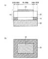
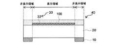
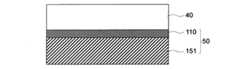
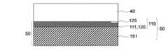
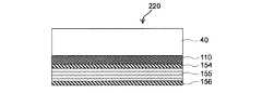
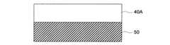
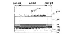
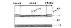
図1(a)および図2(a)に示すように、本実施の形態の表示装置は、LCD、PDP、有機ELなどの表示部50と、表示部50に対して観察者側に配置され、表示領域と非表示領域とを有する表示用前面板40と、を備えている。なお、本実施の形態の表示装置は、表示用前面板40の周縁部を支える枠体がないものや、表示用前面板40が枠体によって挟持されているだけで表示用前面板40の観察者側の表面が枠体によって覆われていないものを想定している。  As shown in FIG. 1A and FIG. 2A, the display device of the present embodiment is arranged on the viewer side with respect to thedisplay unit 50 such as an LCD, PDP, and organic EL, and thedisplay unit 50. And adisplay front plate 40 having a display area and a non-display area. Note that the display device according to the present embodiment does not have a frame that supports the peripheral portion of thedisplay front plate 40, or thedisplay front plate 40 is observed only by thedisplay front plate 40 being held between the frames. It is assumed that the surface on the person side is not covered by the frame.

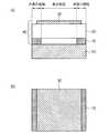
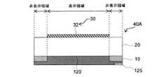
上記の表示用前面板40は、表示部50を保護するためのものであり、0.5mm以上の厚みからなっている。また、表示用前面板40は、面方向に沿って表示領域と非表示領域とを有している。この表示用前面板40は、略矩形状からなりガラス基板などの透明基板20と、透明基板20の観察者側(図1の上方側)に反射防止材料を含む塗布液が塗布されることで設けられた反射防止膜30と、透明基板20の表示部側(図1の下方側)に設けられて透明基板20の周縁部に位置して非表示領域を形成する意匠層10と、を備えている。  Thedisplay front plate 40 is for protecting thedisplay unit 50 and has a thickness of 0.5 mm or more. Thedisplay front plate 40 has a display area and a non-display area along the surface direction. Thedisplay front plate 40 has a substantially rectangular shape, and a coating liquid containing an antireflection material is applied to thetransparent substrate 20 such as a glass substrate and the observer side (upper side in FIG. 1) of thetransparent substrate 20. Anantireflection film 30 provided, and adesign layer 10 provided on the display portion side (lower side in FIG. 1) of thetransparent substrate 20 and positioned on the peripheral portion of thetransparent substrate 20 to form a non-display region. ing.

このうち、反射防止膜30は低屈折率層のみからなる単層構成でもよいが、多層構造からなってもよい。そして、多層構造からなる場合には、一般に、最表面に適切な膜厚の低屈折率層を形成し、さらに高屈折率層などの層を低屈折率層の下層に設けることで作製することができ、より具体的には、透明基板20側から順番に、高/低屈折率層、中/高/低屈折率層、ハードコート層/中/高/低屈折率層などからなる。また、反射防止膜30をドライ法で形成すると、コストが高くなり生産性が低くなることから、本実施の形態の反射防止膜30は、ダイコート法、スピンコート法またはディップコート法などのウエット法で形成される。なお、材料の屈折率を下げるには、フッ素原子を導入したり、密度を下げたり(空隙を導入したり)することで実現することができる。なお、反射防止膜30に用いられる材料などについては、特開2005−43749号に開示されており、当該特開2005−43749号に開示されている材料を用いることができる。  Among these, theantireflection film 30 may have a single-layer structure including only a low refractive index layer, or may have a multilayer structure. In the case of a multilayer structure, generally, a low refractive index layer having an appropriate film thickness is formed on the outermost surface, and a layer such as a high refractive index layer is provided below the low refractive index layer. More specifically, in order from thetransparent substrate 20 side, a high / low refractive index layer, a medium / high / low refractive index layer, a hard coat layer / medium / high / low refractive index layer, and the like. In addition, when theantireflection film 30 is formed by a dry method, the cost is increased and the productivity is lowered. Therefore, theantireflection film 30 of this embodiment is formed by a wet method such as a die coating method, a spin coating method, or a dip coating method. Formed with. Note that the refractive index of the material can be lowered by introducing fluorine atoms or lowering the density (introducing voids). In addition, about the material etc. which are used for theanti-reflective film 30, it is disclosed by Unexamined-Japanese-Patent No. 2005-43749, The material currently disclosed by the said Unexamined-Japanese-Patent No. 2005-43749 can be used.

また、意匠層10は、グラビア印刷、オフセット印刷、スクリーン印刷、転写シートからの転写印刷などの公知の印刷法、または手描きなどによってインキによって形成することができる。また、全面ベタ柄の場合は、グラビアコート、ロールコート、スプレーコートなどの公知の塗工法によって塗料で形成することもできる。使用するインキまたは塗料としては、バインダーとして、塩素化ポリエチレン、塩素化ポリプロピレン等の塩素化ポリオレフィン、ポリエステル樹脂、ウレタン樹脂、アクリル樹脂、酢酸ビニル樹脂、塩化ビニル−酢酸ビニル共重合体、セルロース系樹脂などの樹脂を、一種又は二種以上混合したものに着色剤、適宜その他添加剤を添加した物を用いることができる。なお、より詳細については、特開2005−43749号に開示されており、当該特開2005−43749号に開示されている着色剤などを用いることができる。  Thedesign layer 10 can be formed of ink by a known printing method such as gravure printing, offset printing, screen printing, transfer printing from a transfer sheet, or hand drawing. In the case of a solid pattern, it can be formed with a paint by a known coating method such as gravure coating, roll coating or spray coating. As ink or paint to be used, binder, chlorinated polyolefin such as chlorinated polyethylene, chlorinated polypropylene, polyester resin, urethane resin, acrylic resin, vinyl acetate resin, vinyl chloride-vinyl acetate copolymer, cellulose resin, etc. A resin prepared by adding one or two or more of these resins with a colorant and optionally other additives can be used. Details are disclosed in JP-A-2005-43749, and a colorant disclosed in JP-A-2005-43749 can be used.

また、反射防止膜30は、非表示領域に位置した周縁部の少なくとも一部で除去されており、図1(b)および図2(b)に示すように、本実施の形態の反射防止膜30は周縁部の全周にわたって除去されている。なお、反射防止膜30は、図1(a)(b)に示すように非表示領域に位置する部分の全てが除去される態様もあれば、図2(a)(b)に示すように非表示領域に位置する部分の一部が除去される態様もある。ところで、図1(b)および図2(b)においては、反射防止膜30の位置と意匠層10の位置との関係を明確に示すために、透明基板20を図示していない。このことは、図3(b)、図4(b)、図7(a)−(c)および図8(a)−(c)のいずれにも当てはまる。  Further, theantireflection film 30 is removed at at least a part of the peripheral edge located in the non-display area, and as shown in FIGS. 1B and 2B, the antireflection film of the present embodiment. 30 is removed over the entire periphery. In addition, as shown in FIGS. 2 (a) and 2 (b), theantireflection film 30 has a mode in which all of the portions located in the non-display area are removed as shown in FIGS. 1 (a) and 1 (b). There is also an aspect in which a part of the portion located in the non-display area is removed. Incidentally, in FIGS. 1B and 2B, thetransparent substrate 20 is not shown in order to clearly show the relationship between the position of theantireflection film 30 and the position of thedesign layer 10. This applies to any of FIGS. 3 (b), 4 (b), 7 (a)-(c) and 8 (a)-(c).

図2(a)(b)に示すように非表示領域に位置する部分の一部が除去される態様においては、例えば、非表示領域の幅が2.0mm以上からなる場合において、反射防止膜30は、その幅が0.5mm〜2.0mmで除去される(透明基板20の外縁から0.5mm〜2.0mmの幅で除去される)。このように反射防止膜30を0.5mm〜2.0mmの幅で除去することによって、反射防止膜30の周縁部に形成される盛り上がり部31(図5(c)および図6(c)参照)を除去することができる。  As shown in FIGS. 2A and 2B, in the aspect in which a part of the portion located in the non-display area is removed, for example, when the width of the non-display area is 2.0 mm or more, theantireflection film 30 is removed with a width of 0.5 mm to 2.0 mm (removed from the outer edge of thetransparent substrate 20 with a width of 0.5 mm to 2.0 mm). Thus, by removing theantireflection film 30 with a width of 0.5 mm to 2.0 mm, the raised portion 31 (see FIG. 5C and FIG. 6C) formed on the peripheral edge of the antireflection film 30. ) Can be removed.

なお、反射防止膜30の盛り上がり部31は、表面張力や反射防止膜30を形成するための塗布液の出し方によって異なる大きさで形成される。より具体的には、例えばダイコート法、スピンコート法またはディップコート法などのウエット法を用いた場合には塗布液の表面張力によって周縁部が盛り上がってしまうし、例えばダイコート法を用いた場合には塗布液の塗布を開始する位置と塗布液の塗布が終了する位置で単位面積あたりの塗布量が多くなってしまう。しかしながら、これらの原因は、表示用前面板40の大きさに起因するものではないため、反射防止膜30の周縁位置から2.0mmほど除去すれば、表示用前面板40の大きさに関わりなく盛り上がり部31を除去することができる。  The raisedportion 31 of theantireflection film 30 is formed in different sizes depending on the surface tension and how to apply the coating liquid for forming theantireflection film 30. More specifically, for example, when a wet method such as a die coating method, a spin coating method, or a dip coating method is used, the peripheral portion rises due to the surface tension of the coating solution. For example, when a die coating method is used, The application amount per unit area increases at the position where the application of the application liquid is started and the position where the application of the application liquid ends. However, these causes are not caused by the size of thedisplay front plate 40. Therefore, if the removal is performed by about 2.0 mm from the peripheral position of theantireflection film 30, thedisplay front plate 40 is not affected. The raisedportion 31 can be removed.

ところで、反射防止膜30がダイコート法で形成される際には、図3(b)および図4(b)に示すように、塗布液の塗布を行う方向(図3(b)および図4(b)の左右方向)に直交する透明基板20の一辺に対応する位置と当該一辺に対向する他辺に対応する位置において、反射防止膜30が除去されていれば足りる。すなわち、ダイコート法を用いて反射防止膜30を形成する場合には、塗布液の塗布を開始する位置と塗布液の塗布が終了する位置で単位面積あたりの塗布量が多くなってしまうことが盛り上がり部31の形成に大きく寄与していることから、塗布液の塗布を開始する位置と塗布液の塗布が終了する位置にのみ盛り上がり部31が形成される。このため、塗布を開始する位置である透明基板20の一辺に対応する位置(図3(a)(b)および図4(a)(b)における左側の辺に沿った領域)と、塗布が終了する位置である透明基板20の一辺に対向する他辺に対応する位置(図3(a)(b)および図4(a)(b)における右側の辺に沿った領域)において、反射防止膜30が除去されていれば足りる。  By the way, when theantireflection film 30 is formed by the die coating method, as shown in FIGS. 3B and 4B, the direction in which the coating liquid is applied (FIG. 3B and FIG. 4B). It is sufficient that theantireflection film 30 is removed at a position corresponding to one side of thetransparent substrate 20 orthogonal to the horizontal direction b) and a position corresponding to the other side facing the one side. That is, when theantireflection film 30 is formed by using the die coating method, the amount of application per unit area increases at the position where the application of the application liquid is started and the position where the application of the application liquid ends. Since it greatly contributes to the formation of theportion 31, the raisedportion 31 is formed only at the position where the application of the coating liquid is started and the position where the application of the coating liquid is completed. For this reason, the position corresponding to one side of thetransparent substrate 20 that is the position where the application is started (the region along the left side in FIGS. 3A and 3B and FIGS. 4A and 4B), and the application Antireflection at the position corresponding to the other side opposite to one side of thetransparent substrate 20 that is the end position (the region along the right side in FIGS. 3A and 3B and FIGS. 4A and 4B) It is sufficient if thefilm 30 is removed.

なおこの場合にも、上記と同様、反射防止膜30は、透明基板20の一辺に対応する位置と一辺に対向する他辺に対応する位置において、図3(a)(b)に示すように非表示領域に位置する部分の全てが除去される態様もあれば、図4(a)(b)に示すように非表示領域に位置する部分の一部が除去される態様もある。そして、非表示領域に位置する部分の一部が除去される態様においては、上記と同様、非表示領域の幅が2.0mm以上からなる場合において、反射防止膜30はその幅が0.5mm〜2.0mmで除去されることとなる。  Also in this case, as described above, theantireflection film 30 is located at a position corresponding to one side of thetransparent substrate 20 and a position corresponding to the other side opposite to the one side, as shown in FIGS. There is an aspect in which all of the part located in the non-display area is removed, and there is also an aspect in which a part of the part located in the non-display area is removed as shown in FIGS. And in the aspect from which a part of part located in a non-display area | region is removed, when the width | variety of a non-display area | region consists of 2.0 mm or more like the above, the width | variety of theantireflection film 30 is 0.5 mm. It will be removed at ~ 2.0 mm.

次に、このような構成からなる本実施の形態の作用および効果について説明する。
[反射防止膜30の非表示領域に位置する部分の全てを除去]
Next, the operation and effect of the present embodiment having such a configuration will be described.
[Removes all portions ofantireflection film 30 located in the non-display area]

最初に、反射防止膜30が、非表示領域に位置する部分の全てで除去されている表示用前面板40および表示装置の製造方法について説明する。  First, a method for manufacturing thedisplay front plate 40 and the display device in which theantireflection film 30 is removed in all of the portions located in the non-display area will be described.

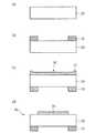
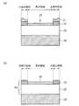
まず、透明基板20が準備される(図5(a)参照)。  First, thetransparent substrate 20 is prepared (see FIG. 5A).

次に、透明基板20の表示部側(図5(b)の上方側)の周縁部に意匠層10が印刷されて形成される(図5(b)参照)。  Next, thedesign layer 10 is printed and formed on the peripheral edge of thetransparent substrate 20 on the display portion side (the upper side in FIG. 5B) (see FIG. 5B).

次に、意匠層10が載置された透明基板20が180°反転され、透明基板20の観察者側(図5(c)の上方側)の全面に反射防止材料を含む塗布液が直接塗布されて反射防止膜30が形成される(図5(c)参照)。このとき、塗布液は、ダイコート法、スピンコート法またはディップコート法などのウエット法で塗布される。  Next, thetransparent substrate 20 on which thedesign layer 10 is placed is inverted 180 °, and a coating liquid containing an antireflection material is directly applied to the entire surface of thetransparent substrate 20 on the observer side (the upper side in FIG. 5C). Thus, theantireflection film 30 is formed (see FIG. 5C). At this time, the coating solution is applied by a wet method such as a die coating method, a spin coating method, or a dip coating method.

次に、反射防止膜30が周縁部の全周にわたって除去される(図1(b)参照)。このとき、本実施の形態の反射防止膜30は、非表示領域に位置する部分の全てで除去されることとなる(図1(a)(b)および図5(d)参照)。  Next, theantireflection film 30 is removed over the entire periphery (see FIG. 1B). At this time, theantireflection film 30 of the present embodiment is removed in all the portions located in the non-display area (see FIGS. 1A and 1B and FIG. 5D).

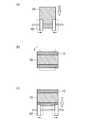
なお、反射防止膜30を除去する方法としては、ローラ、粘着膜を有するテープ、スキージ、ワイプなどによって除去することが考えられる。この点、ローラを用いる場合には、例えば図7(a)(c)に示すように間隔を自在に調整することができる一対のローラ60や、図8(a)(c)に示すように幅の異なり平行に配置された二つの一対のローラ60a,60bなどを用いることができる。なお、ローラとしては、例えば多孔性のスポンジローラなどを用いることができる。  As a method for removing theantireflection film 30, it is conceivable to remove it by a roller, a tape having an adhesive film, a squeegee, a wipe, or the like. In this regard, when rollers are used, for example, as shown in FIGS. 7A and 7C, a pair ofrollers 60 whose intervals can be freely adjusted, or as shown in FIGS. Two pairs ofrollers 60a and 60b arranged in parallel with different widths can be used. For example, a porous sponge roller can be used as the roller.

図7(a)(c)に示すような一対のローラ60を用いて反射防止膜30を除去する場合には、まず、図7(a)に示すように、間隔の調整されたローラ60によって、対向する一対の辺に沿って反射防止膜30を周縁部で除去する。次に、図7(b)に示すように、反射防止膜30の積層された透明基板20を90°回転させる。(なお、このように透明基板20を90°回転させる代わりに、一対のスポンジローラ60を90°回転させてもよい。)次に、図7(c)に示すように、間隔の調整されたローラ60によって、上記で反射防止膜30を既に除去した一対の辺と異なる一対の辺に沿って反射防止膜30を周縁部で除去する。なお、一対のローラ60の間隔は、透明基板20の方向に合わせて調整される(図7(a)(c)参照)。  When theantireflection film 30 is removed by using a pair ofrollers 60 as shown in FIGS. 7A and 7C, first, as shown in FIG. Theantireflection film 30 is removed at the peripheral edge along a pair of opposing sides. Next, as shown in FIG. 7B, thetransparent substrate 20 on which theantireflection film 30 is laminated is rotated by 90 °. (Instead of rotating thetransparent substrate 20 by 90 ° in this way, the pair ofsponge rollers 60 may be rotated by 90 °.) Next, as shown in FIG. Theroller 60 removes theantireflection film 30 at the peripheral edge along a pair of sides different from the pair of sides from which theantireflection film 30 has already been removed. In addition, the space | interval of a pair ofroller 60 is adjusted according to the direction of the transparent substrate 20 (refer Fig.7 (a) (c)).

また、図8(a)(c)に示すような平行に配置された二つの一対のローラ60a,60bを用いて反射防止膜30を除去する場合には、まず、図8(a)に示すように、ローラ60aによって、対向する一対の辺に沿って反射防止膜30を周縁部で除去する。次に、図8(b)に示すように、反射防止膜30の積層された透明基板20を90°回転させる。次に、図8(c)に示すように、ローラ60bによって、上記で反射防止膜30を既に除去した一対の辺と異なる一対の辺に沿って反射防止膜30を周縁部で除去する。  When theantireflection film 30 is removed using two pairs ofrollers 60a and 60b arranged in parallel as shown in FIGS. 8A and 8C, first, as shown in FIG. As described above, theantireflection film 30 is removed at the peripheral edge along the pair of opposite sides by theroller 60a. Next, as shown in FIG. 8B, thetransparent substrate 20 on which theantireflection film 30 is laminated is rotated by 90 °. Next, as shown in FIG. 8C, theantireflection film 30 is removed at the peripheral edge along a pair of sides different from the pair of sides from which theantireflection film 30 has already been removed by theroller 60b.

また、このように反射防止膜30を除去する際には、より容易に反射防止膜30を除去するために、溶剤、アルカリ性の薬液、酸性の薬液、水、アセトンなどを用いることができる。この点、反射防止膜30が樹脂材料からなる場合には、例えば溶剤とアルカリ性の薬液の混合液、溶剤と酸性の薬液の混合液などを用いることができ、反射防止膜30が無機材料からなる場合には、例えば水やアセトンなどを用いることができる。なお、ここで溶剤としては、例えばメチルプロピルアセテート(PGMEA)、メチルイソブチルケトン(MIBK)、メチルエチルケトン(MEK)などを挙げることができる。  Further, when removing theantireflection film 30 in this way, a solvent, an alkaline chemical solution, an acidic chemical solution, water, acetone, or the like can be used in order to remove theantireflection film 30 more easily. In this regard, when theantireflection film 30 is made of a resin material, for example, a mixed solution of a solvent and an alkaline chemical solution, a mixed solution of a solvent and an acidic chemical solution, or the like can be used, and theantireflection film 30 is made of an inorganic material. In some cases, for example, water or acetone can be used. Here, examples of the solvent include methyl propyl acetate (PGMEA), methyl isobutyl ketone (MIBK), and methyl ethyl ketone (MEK).

また、反射防止膜30を除去する方法として、上記のようなローラ60,60a,60bを用いるのではなく、粘着膜を有するテープを用いる場合には、テープの粘着膜を反射防止膜30の周縁部に貼り付け、当該テープを透明基板20から離隔させることで反射防止膜30の周縁部を除去することができる。  In addition, as a method of removing theantireflection film 30, when using a tape having an adhesive film instead of using therollers 60, 60a, 60b as described above, the adhesive film of the tape is used as the peripheral edge of theantireflection film 30. The peripheral portion of theantireflection film 30 can be removed by attaching the tape to the portion and separating the tape from thetransparent substrate 20.

このように反射防止膜30の周縁部を除去することで、膜厚が不均一になっている盛り上がり部31を除去することができ、その結果、反射防止膜30の膜厚を全面にわたって均一にすることができる。  By removing the peripheral portion of theantireflection film 30 in this way, the raisedportion 31 having a non-uniform film thickness can be removed. As a result, the film thickness of theantireflection film 30 is made uniform over the entire surface. can do.

上記のように反射防止膜30が周縁部で除去されると、反射防止膜30が乾燥された後で露光されたり、乾燥された後で加熱されたり、乾燥された後で露光および加熱されたり、乾燥のみされたりすることで、反射防止膜30が硬化される。(なお一般に、反射防止材料に紫外線硬化樹脂が含まれている場合には反射防止膜30を露光することで硬化させ、反射防止材料に熱硬化樹脂が含まれている場合には反射防止膜30を加熱することで硬化させることとなる。)以上の工程によって、表示用前面板40が製造される。  When theantireflection film 30 is removed at the peripheral edge as described above, theantireflection film 30 is exposed after being dried, heated after being dried, or exposed and heated after being dried. By being only dried, theantireflection film 30 is cured. (In general, when the antireflection material contains an ultraviolet curable resin, theantireflection film 30 is cured by exposure, and when the antireflection material contains a thermosetting resin, theantireflection film 30 is cured. Thedisplay front plate 40 is manufactured through the above steps.

そして、このように製造された表示用前面板40を表示部50の観察者側に配置して取り付けることで表示装置が製造される。  And the display apparatus is manufactured by arrange | positioning and attaching thedisplay front board 40 manufactured in this way to the observer side of thedisplay part 50. FIG.

本実施の形態によれば、反射防止膜30が周縁部の全周にわたって除去される。このため、表面張力や塗布液の出し方によって形成される反射防止膜30の盛り上がり部31を除去することができる。この結果、反射防止膜30の膜厚を全面にわたって均一にすることができ、ひいては、反射率分布を均一にして反射ムラを防止することができる。  According to the present embodiment, theantireflection film 30 is removed over the entire periphery. For this reason, the risingpart 31 of theanti-reflective film 30 formed by surface tension or how to apply the coating liquid can be removed. As a result, the film thickness of theantireflection film 30 can be made uniform over the entire surface, and consequently the reflectance distribution can be made uniform to prevent uneven reflection.

また、本実施の形態では、反射防止膜30は、非表示領域に位置する部分の全てで除去される。このため、表示領域と非表示領域との間の界面と、反射防止膜30が存在する領域と反射防止膜30が存在しない領域との間の界面を合わせることができ、観察者側から見たときの反射ムラをより確実に防止することができる。  In the present embodiment, theantireflection film 30 is removed at all of the portions located in the non-display area. Therefore, the interface between the display area and the non-display area can be matched with the interface between the area where theantireflection film 30 is present and the area where theantireflection film 30 is not present, as viewed from the observer side. It is possible to more surely prevent uneven reflection at the time.

なお、上記では、反射防止膜30を周縁部の全周にわたって除去する態様を用いて説明したが、これに限られることはない。例えば反射防止材料を含む塗布液をダイコート法で塗布する場合には、塗布液の塗布を開始する位置と塗布液の塗布が終了する位置で単位面積あたりの塗布量が多くなってしまうことが盛り上がり部31の形成に大きく寄与しているので、塗布液の塗布を開始する側の一辺と塗布液の塗布が終了する側の他辺(前記一辺に対向する他辺)において反射防止膜30を除去すればよい(図3(a)(b)参照)。このため、この場合には、対向する一つの一対の辺(塗布液の塗布を開始する側の一辺と塗布液の塗布が終了する側の他辺)に沿って反射防止膜30を周縁部で除去すれば足りる。  In the above description, theantireflection film 30 has been described as being removed over the entire periphery, but the present invention is not limited to this. For example, when a coating solution containing an antireflection material is applied by the die coating method, the amount of coating per unit area increases at the position where the coating solution application starts and the position where the coating solution application ends. Since it greatly contributes to the formation of theportion 31, theantireflection film 30 is removed on one side where the coating liquid application is started and on the other side where the coating liquid application ends (the other side opposite to the one side). (See FIGS. 3A and 3B). For this reason, in this case, theantireflection film 30 is disposed at the peripheral portion along one pair of opposing sides (one side on the side where the coating liquid application starts and the other side on the side where the coating liquid application ends). It is enough to remove it.

[反射防止膜30の非表示領域に位置する部分の一部を除去]
次に、反射防止膜30が、非表示領域に位置する部分の一部で除去されている表示用前面板40および表示装置の製造方法について説明する。なお、上述した反射防止膜30が非表示領域に位置する部分の全てで除去されている態様と重複する部分については適宜省略しつつ説明する。
[Removal of a portion of theantireflection film 30 located in the non-display area]
Next, a method for manufacturing thedisplay front plate 40 and the display device in which theantireflection film 30 is removed at a part of the portion located in the non-display area will be described. In addition, the part which overlaps with the aspect from which theantireflection film 30 mentioned above is removed in all the parts located in a non-display area | region is demonstrated, abbreviate | omitting suitably.

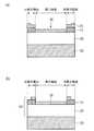
まず、透明基板20が準備される(図6(a)参照)。  First, thetransparent substrate 20 is prepared (see FIG. 6A).

次に、透明基板20の表示部側(図6(b)の上方側)の周縁部に意匠層10が印刷されて形成される(図6(b)参照)。このとき、意匠層10の幅は2.0mm以上からなっており、非表示領域の幅は2.0mm以上からなっている。  Next, thedesign layer 10 is printed and formed on the peripheral edge of thetransparent substrate 20 on the display portion side (the upper side in FIG. 6B) (see FIG. 6B). At this time, the width of thedesign layer 10 is 2.0 mm or more, and the width of the non-display area is 2.0 mm or more.

次に、意匠層10が載置された透明基板20が180°反転され、透明基板20の観察者側(図6(c)の上方側)の全面に反射防止材料を含む塗布液が直接塗布されて反射防止膜30が形成される(図6(c)参照)。このとき、塗布液は、ダイコート法、スピンコート法またはディップコート法などのウエット法で塗布される。  Next, thetransparent substrate 20 on which thedesign layer 10 is placed is inverted 180 °, and a coating liquid containing an antireflection material is directly applied to the entire surface of thetransparent substrate 20 on the observer side (upper side in FIG. 6C). Thus, theantireflection film 30 is formed (see FIG. 6C). At this time, the coating solution is applied by a wet method such as a die coating method, a spin coating method, or a dip coating method.

次に、反射防止膜30が周縁部の全周にわたって除去される(図2(b)参照)。このとき、本実施の形態の反射防止膜30は、非表示領域に位置する部分の一部で除去されることとなる(図2(a)(b)および図6(d)参照)。より具体的には、反射防止膜30の周縁部が0.5mm〜2.0mmの幅で除去される(つまり、透明基板20の外周から0.5mm〜2.0mmの幅で反射防止膜30が除去される)。  Next, theantireflection film 30 is removed over the entire periphery (see FIG. 2B). At this time, theantireflection film 30 of the present embodiment is removed at a part of the portion located in the non-display area (see FIGS. 2A and 2B and FIG. 6D). More specifically, the peripheral portion of theantireflection film 30 is removed with a width of 0.5 mm to 2.0 mm (that is, theantireflection film 30 with a width of 0.5 mm to 2.0 mm from the outer periphery of the transparent substrate 20). Is removed).

この際、反射防止膜30は、ローラ、粘着膜を有するテープ、スキージ、ワイプなどによって除去することができる。また、このように反射防止膜30を除去する際には、より容易に反射防止膜30を除去するために、溶剤、アルカリ性の薬液、酸性の薬液、水、アセトンなどを用いることができる。  At this time, theantireflection film 30 can be removed by a roller, a tape having an adhesive film, a squeegee, a wipe, or the like. Further, when removing theantireflection film 30 in this way, a solvent, an alkaline chemical solution, an acidic chemical solution, water, acetone, or the like can be used in order to remove theantireflection film 30 more easily.

このように反射防止膜30の周縁部を除去することで、膜厚が不均一になっている盛り上がり部31を除去することができ、その結果、反射防止膜30の膜厚を全面にわたって均一にすることができる。  By removing the peripheral portion of theantireflection film 30 in this way, the raisedportion 31 having a non-uniform film thickness can be removed. As a result, the film thickness of theantireflection film 30 is made uniform over the entire surface. can do.

上記のように反射防止膜30が周縁部で除去されると、反射防止膜30が乾燥された後で露光されたり、乾燥された後で加熱されたり、乾燥された後で露光および加熱されたり、乾燥のみされたりすることで、反射防止膜30が硬化される。以上の工程によって、表示用前面板40が製造される。  When theantireflection film 30 is removed at the peripheral edge as described above, theantireflection film 30 is exposed after being dried, heated after being dried, or exposed and heated after being dried. By being only dried, theantireflection film 30 is cured. Thedisplay front plate 40 is manufactured through the above steps.

そして、このように製造された表示用前面板40を表示部50の観察者側に配置して取り付けることで表示装置が製造される。  And the display apparatus is manufactured by arrange | positioning and attaching thedisplay front board 40 manufactured in this way to the observer side of thedisplay part 50. FIG.

本実施の形態によれば、反射防止膜30が周縁部の全周にわたって除去される。このため、表面張力や塗布液の出し方によって形成される反射防止膜30の盛り上がり部31を除去することができる。この結果、反射防止膜30の膜厚を全面にわたって均一にすることができ、ひいては、反射率分布を均一にして反射ムラを防止することができる。  According to the present embodiment, theantireflection film 30 is removed over the entire periphery. For this reason, the risingpart 31 of theanti-reflective film 30 formed by surface tension or how to apply the coating liquid can be removed. As a result, the film thickness of theantireflection film 30 can be made uniform over the entire surface, and consequently the reflectance distribution can be made uniform to prevent uneven reflection.

なお、上記では、反射防止膜30を周縁部の全周にわたって除去する態様を用いて説明したが、これに限られることはない。例えば反射防止材料を含む塗布液をダイコート法で塗布する場合には、塗布液の塗布を開始する側の一辺と塗布液の塗布が終了する側の他辺(前記一辺に対向する他辺)において、0.5mm〜2.0mmの幅で反射防止膜30を除去すればよい(図4(a)(b)参照)。  In the above description, theantireflection film 30 has been described as being removed over the entire periphery, but the present invention is not limited to this. For example, in the case of applying a coating liquid containing an antireflection material by a die coating method, on one side where coating liquid application starts and on the other side where coating liquid coating ends (other side opposite to the one side) Theantireflection film 30 may be removed with a width of 0.5 mm to 2.0 mm (see FIGS. 4A and 4B).

次に、本実施の形態の実施例と比較例について説明する。  Next, examples of the present embodiment and comparative examples will be described.

(実施例)
まず、ガラス基板(透明基板)20を準備した。次に、ガラス基板20の表示部側(裏面)の周縁部に意匠層10を印刷して形成した。次に、ガラス基板20の観察者側(表面)の全面に反射防止材料を含む塗布液を、ダイコート法によって周縁部から直接塗布した。次に、反射防止膜30を周縁部の全周にわたって除去した。このとき、反射防止膜30は、溶剤付きのスポンジローラ60によって、外縁から2.0mmの幅で除去された。このようにして周縁部が除去された反射防止膜30の膜厚・反射率分布を測定したところ、膜厚・反射率分布は平均値±10%の範囲であった。
(Example)
First, a glass substrate (transparent substrate) 20 was prepared. Next, thedesign layer 10 was printed and formed on the peripheral portion on the display unit side (back surface) of theglass substrate 20. Next, a coating solution containing an antireflective material was applied directly from the peripheral edge to the entire surface of the observer side (surface) of theglass substrate 20 by a die coating method. Next, theantireflection film 30 was removed over the entire periphery. At this time, theantireflection film 30 was removed from the outer edge with a width of 2.0 mm by asponge roller 60 with a solvent. When the film thickness / reflectance distribution of theantireflection film 30 from which the peripheral portion was removed in this way was measured, the film thickness / reflectance distribution was in the range of an average value ± 10%.

(比較例)
まず、ガラス基板20を準備した。次に、ガラス基板20の表示部側(裏面)の周縁部に意匠層10を印刷して形成した。次に、ガラス基板20の観察者側(表面)の全面に反射防止材料を含む塗布液を、ダイコート法によって周縁部から直接塗布した。このようにして形成された反射防止膜30の膜厚・反射率分布を測定したところ、外縁から2.0mmの幅までの領域で膜厚・反射率分布が不均一になっており、膜厚・反射率分布は平均値±74%の範囲であった。
(Comparative example)
First, theglass substrate 20 was prepared. Next, thedesign layer 10 was printed and formed on the peripheral portion on the display unit side (back surface) of theglass substrate 20. Next, a coating solution containing an antireflective material was applied directly from the peripheral edge to the entire surface of the observer side (surface) of theglass substrate 20 by a die coating method. When the film thickness / reflectance distribution of theantireflection film 30 formed in this way was measured, the film thickness / reflectance distribution was uneven in the region from the outer edge to the width of 2.0 mm. -The reflectance distribution was in the range of the average value ± 74%.

これらのことから、上記の実施例のように、外縁から2.0mmの幅で反射防止膜30を除去することで、膜厚・反射率分布を平均値±10%とすることができ、比較例での平均値±74%よりも膜厚・反射率分布を格段に均一にできることを確認することができた。  From these facts, the thickness / reflectance distribution can be set to an average value ± 10% by removing theantireflection film 30 with a width of 2.0 mm from the outer edge as in the above embodiment. It was confirmed that the film thickness / reflectance distribution could be remarkably made uniform than the average value ± 74% in the example.

第2の実施の形態
次に、図9乃至図12により、本発明の第2の実施の形態について説明する。
SecondEmbodiment Next, asecond embodiment of the present invention will be described with reference to FIGS.

第1の実施の形態は、透明基板20の表示部側に意匠層10が設けられている態様であったが、第2の実施の形態では、透明基板20の観察者側に意匠層10が設けられている態様になっている。第2の実施の形態において、その他の構成は、第1の実施の形態と略同一の態様となっている。  In the first embodiment, thedesign layer 10 is provided on the display unit side of thetransparent substrate 20. However, in the second embodiment, thedesign layer 10 is provided on the observer side of thetransparent substrate 20. It is the aspect provided. In the second embodiment, other configurations are substantially the same as those in the first embodiment.

図9乃至図12に示す第2の実施の形態において、図1乃至図8に示す第1の実施の形態と同一部分には同一符号を付して詳細な説明は省略する。
[反射防止膜30の非表示領域に位置する部分の全てを除去]
In the second embodiment shown in FIG. 9 to FIG. 12, the same parts as those in the first embodiment shown in FIG. 1 to FIG.
[Removes all portions ofantireflection film 30 located in the non-display area]

以下、本実施の形態の作用および効果について説明する。最初に、反射防止膜30が、非表示領域に位置する部分の全てで除去されている表示用前面板40および表示装置の製造方法について説明する。なお、第1の実施の形態と重複する部分については適宜省略しつつ説明する。  Hereinafter, the operation and effect of the present embodiment will be described. First, a method for manufacturing thedisplay front plate 40 and the display device in which theantireflection film 30 is removed in all of the portions located in the non-display area will be described. Note that portions overlapping with those of the first embodiment will be described as appropriate.

まず、透明基板20が準備される(図11(a)参照)。  First, thetransparent substrate 20 is prepared (see FIG. 11A).

次に、透明基板20の観察者側(図11(b)の上方側)の周縁部に意匠層10が印刷されて形成される(図11(b)参照)。  Next, thedesign layer 10 is printed and formed on the peripheral portion of thetransparent substrate 20 on the viewer side (the upper side in FIG. 11B) (see FIG. 11B).

次に、透明基板20と意匠層10の観察者側(図11(c)の上方側)の全面に反射防止材料を含む塗布液が直接塗布されて反射防止膜30が形成される(図9(a)および図11(c)参照)。このとき、塗布液は、ダイコート法、スピンコート法またはディップコート法などのウエット法で塗布される。  Next, a coating liquid containing an antireflection material is directly applied to the entire surface of thetransparent substrate 20 and thedesign layer 10 on the viewer side (upper side in FIG. 11C) to form an antireflection film 30 (FIG. 9). (See (a) and FIG. 11 (c)). At this time, the coating solution is applied by a wet method such as a die coating method, a spin coating method, or a dip coating method.

次に、反射防止膜30が周縁部の全周にわたって除去される。このとき、本実施の形態の反射防止膜30は、非表示領域に位置する部分の全てで除去されることとなる(図9(b)および図11(d)参照)。  Next, theantireflection film 30 is removed over the entire periphery. At this time, theantireflection film 30 of the present embodiment is removed in all of the portions located in the non-display area (see FIGS. 9B and 11D).

この際、反射防止膜30は、ローラ、粘着膜を有するテープ、スキージ、ワイプなどによって除去することができる。また、このように反射防止膜30を除去する際には、より容易に反射防止膜30を除去するために、溶剤、アルカリ性の薬液、酸性の薬液、水、アセトンなどを用いることができる。  At this time, theantireflection film 30 can be removed by a roller, a tape having an adhesive film, a squeegee, a wipe, or the like. Further, when removing theantireflection film 30 in this way, a solvent, an alkaline chemical solution, an acidic chemical solution, water, acetone, or the like can be used in order to remove theantireflection film 30 more easily.

このように反射防止膜30の周縁部を除去することで、膜厚が不均一になっている盛り上がり部31を除去することができ、その結果、反射防止膜30の膜厚を全面にわたって均一にすることができる。  By removing the peripheral portion of theantireflection film 30 in this way, the raisedportion 31 having a non-uniform film thickness can be removed. As a result, the film thickness of theantireflection film 30 is made uniform over the entire surface. can do.

上記のように反射防止膜30が周縁部で除去されると、反射防止膜30が乾燥された後で露光されたり、乾燥された後で加熱されたり、乾燥された後で露光および加熱されたり、乾燥のみされたりすることで、反射防止膜30が硬化される。以上の工程によって、表示用前面板40が製造される。  When theantireflection film 30 is removed at the peripheral edge as described above, theantireflection film 30 is exposed after being dried, heated after being dried, or exposed and heated after being dried. By being only dried, theantireflection film 30 is cured. Thedisplay front plate 40 is manufactured through the above steps.

そして、このように製造された表示用前面板40を表示部50の観察者側に配置して取り付けることで表示装置が製造される。  And the display apparatus is manufactured by arrange | positioning and attaching thedisplay front board 40 manufactured in this way to the observer side of thedisplay part 50. FIG.

本実施の形態によれば、反射防止膜30が周縁部の全周にわたって除去される。このため、表面張力や塗布液の出し方によって形成される反射防止膜30の盛り上がり部31を除去することができる。この結果、反射防止膜30の膜厚を全面にわたって均一にすることができ、ひいては、反射率分布を均一にして反射ムラを防止することができる。  According to the present embodiment, theantireflection film 30 is removed over the entire periphery. For this reason, the risingpart 31 of theanti-reflective film 30 formed by surface tension or how to apply the coating liquid can be removed. As a result, the film thickness of theantireflection film 30 can be made uniform over the entire surface, and consequently the reflectance distribution can be made uniform to prevent uneven reflection.

また、本実施の形態では、反射防止膜30は、非表示領域に位置する部分の全てで除去される。このため、表示領域と非表示領域との間の界面と、反射防止膜30が存在する領域と反射防止膜30が存在しない領域との間の界面を合わせることができ、観察者側から見たときの反射ムラをより確実に防止することができる。  In the present embodiment, theantireflection film 30 is removed at all of the portions located in the non-display area. Therefore, the interface between the display area and the non-display area can be matched with the interface between the area where theantireflection film 30 is present and the area where theantireflection film 30 is not present, as viewed from the observer side. It is possible to more surely prevent uneven reflection at the time.

また、本実施の形態によれば、透明基板20の観察者側に非表示領域を形成する意匠層10が設けられている。このため、意匠層10のある非表示領域において透明基板20で外光が反射することを防止することができ、外光が映り込むことを防止することができる。このため、表示装置が本来意図している表示特性を維持することができる。  Moreover, according to this Embodiment, thedesign layer 10 which forms a non-display area | region in the observer side of thetransparent substrate 20 is provided. For this reason, it can prevent that external light reflects in thetransparent substrate 20 in the non-display area | region with thedesign layer 10, and can prevent that external light reflects. For this reason, the display characteristics originally intended by the display device can be maintained.

すなわち、反射防止フィルムが透明基板20に貼られている場合には、反射防止フィルムを通過した外光の透明基板20での反射がどうしても発生してしまう。そして、表示領域に入り込んだ外光は表示部50からの発光によって打ち消されるのに対して、意匠層10のある非表示領域での外光の反射が目立ってしまい、表示装置が本来意図している表示特性が損なわれてしまうこととなる。  That is, when the antireflection film is affixed to thetransparent substrate 20, reflection of external light that has passed through the antireflection film on thetransparent substrate 20 inevitably occurs. The external light entering the display area is canceled by the light emission from thedisplay unit 50, whereas the reflection of the external light in the non-display area where thedesign layer 10 is present is conspicuous, and the display device originally intends. Display characteristics will be lost.

これに対して、本実施の形態によれば、意匠層10が最外面に位置しており、意匠層10のある非表示領域において透明基板20に外光が入り込むことを防止することができる。そして、意匠層10は一般にインキによって形成されるため外光の反射は起こりにくく、また例え意匠層10で外光が反射しても表示装置の表示特性に悪影響を及ぼさないので、表示装置が本来意図している表示特性を維持することができる。  On the other hand, according to this Embodiment, thedesign layer 10 is located in the outermost surface, and it can prevent that external light enters into thetransparent substrate 20 in the non-display area | region with thedesign layer 10. FIG. Since thedesign layer 10 is generally formed of ink, reflection of external light is unlikely to occur, and even if external light is reflected by thedesign layer 10, the display characteristics of the display device are not adversely affected. The intended display characteristics can be maintained.

なお、上記では、反射防止膜30を周縁部の全周にわたって除去する態様を用いて説明したが、これに限られることはない。例えば反射防止材料を含む塗布液をダイコート法で塗布する場合には、塗布液の塗布を開始する側の一辺と塗布液の塗布が終了する側の他辺(前記一辺に対向する他辺)において反射防止膜30を除去すればよい。
[反射防止膜30の非表示領域に位置する部分の一部を除去]
In the above description, theantireflection film 30 has been described as being removed over the entire periphery, but the present invention is not limited to this. For example, in the case of applying a coating liquid containing an antireflection material by a die coating method, on one side where coating liquid application starts and on the other side where coating liquid coating ends (other side opposite to the one side) Theantireflection film 30 may be removed.
[Removal of a portion of theantireflection film 30 located in the non-display area]

次に、反射防止膜30が、非表示領域に位置する部分の一部で除去されている表示用前面板40および表示装置の製造方法について説明する。なお、上述した反射防止膜30が非表示領域に位置する部分の全てで除去されている態様と重複する部分については適宜省略しつつ説明する。  Next, a method for manufacturing thedisplay front plate 40 and the display device in which theantireflection film 30 is removed at a part of the portion located in the non-display area will be described. In addition, the part which overlaps with the aspect from which theantireflection film 30 mentioned above is removed in all the parts located in a non-display area | region is demonstrated, abbreviate | omitting suitably.

まず、透明基板20が準備される(図12(a)参照)。  First, thetransparent substrate 20 is prepared (see FIG. 12A).

次に、透明基板20の観察者側(図12(b)の上方側)の周縁部に意匠層10が印刷されて形成される(図12(b)参照)。このとき、意匠層10の幅は2.0mm以上からなっており、非表示領域の幅は2.0mm以上からなっている。  Next, thedesign layer 10 is printed and formed on the peripheral portion of thetransparent substrate 20 on the viewer side (the upper side of FIG. 12B) (see FIG. 12B). At this time, the width of thedesign layer 10 is 2.0 mm or more, and the width of the non-display area is 2.0 mm or more.

次に、透明基板20と意匠層10の観察者側(図12(c)の上方側)の全面に反射防止材料を含む塗布液が直接塗布されて反射防止膜30が形成される(図10(a)および図12(c)参照)。このとき、塗布液は、ダイコート法、スピンコート法またはディップコート法などのウエット法で塗布される。  Next, a coating solution containing an antireflection material is directly applied to the entire surface of thetransparent substrate 20 and thedesign layer 10 on the viewer side (upper side in FIG. 12C), thereby forming the antireflection film 30 (FIG. 10). (See (a) and FIG. 12 (c)). At this time, the coating solution is applied by a wet method such as a die coating method, a spin coating method, or a dip coating method.

次に、反射防止膜30が周縁部の全周にわたって除去される。このとき、本実施の形態の反射防止膜30は、非表示領域に位置する部分の一部で除去されることとなる(図10(b)および図12(d)参照)。より具体的には、反射防止膜30の周縁部が0.5mm〜2.0mmの幅で除去される(つまり、透明基板20の外周から0.5mm〜2.0mmの幅で反射防止膜30が除去される)。  Next, theantireflection film 30 is removed over the entire periphery. At this time, theantireflection film 30 of the present embodiment is removed at a part of the portion located in the non-display area (see FIGS. 10B and 12D). More specifically, the peripheral portion of theantireflection film 30 is removed with a width of 0.5 mm to 2.0 mm (that is, theantireflection film 30 with a width of 0.5 mm to 2.0 mm from the outer periphery of the transparent substrate 20). Is removed).

この際、反射防止膜30は、ローラ、粘着膜を有するテープ、スキージ、ワイプなどによって除去することができる。また、このように反射防止膜30を除去する際には、より容易に反射防止膜30を除去するために、溶剤、アルカリ性の薬液、酸性の薬液、水、アセトンなどを用いることができる。  At this time, theantireflection film 30 can be removed by a roller, a tape having an adhesive film, a squeegee, a wipe, or the like. Further, when removing theantireflection film 30 in this way, a solvent, an alkaline chemical solution, an acidic chemical solution, water, acetone, or the like can be used in order to remove theantireflection film 30 more easily.

このように反射防止膜30の周縁部を除去することで、膜厚が不均一になっている盛り上がり部31を除去することができ、その結果、反射防止膜30の膜厚を全面にわたって均一にすることができる。  By removing the peripheral portion of theantireflection film 30 in this way, the raisedportion 31 having a non-uniform film thickness can be removed. As a result, the film thickness of theantireflection film 30 is made uniform over the entire surface. can do.

上記のように反射防止膜30が周縁部で除去されると、反射防止膜30が乾燥された後で露光されたり、乾燥された後で加熱されたり、乾燥された後で露光および加熱されたり、乾燥のみされたりすることで、反射防止膜30が硬化される。以上の工程によって、表示用前面板40が製造される。  When theantireflection film 30 is removed at the peripheral edge as described above, theantireflection film 30 is exposed after being dried, heated after being dried, or exposed and heated after being dried. By being only dried, theantireflection film 30 is cured. Thedisplay front plate 40 is manufactured through the above steps.

そして、このように製造された表示用前面板40を表示部50の観察者側に配置して取り付けることで表示装置が製造される。  And the display apparatus is manufactured by arrange | positioning and attaching thedisplay front board 40 manufactured in this way to the observer side of thedisplay part 50. FIG.

本実施の形態によれば、反射防止膜30が周縁部の全周にわたって除去される。このため、表面張力や塗布液の出し方によって形成される反射防止膜30の盛り上がり部31を除去することができる。この結果、反射防止膜30の膜厚を全面にわたって均一にすることができ、ひいては、反射率分布を均一にして反射ムラを防止することができる。  According to the present embodiment, theantireflection film 30 is removed over the entire periphery. For this reason, the risingpart 31 of theanti-reflective film 30 formed by surface tension or how to apply the coating liquid can be removed. As a result, the film thickness of theantireflection film 30 can be made uniform over the entire surface, and consequently the reflectance distribution can be made uniform to prevent uneven reflection.

また、本実施の形態によれば、透明基板20の観察者側に非表示領域を形成する意匠層10が設けられている。このため、意匠層10のある非表示領域において透明基板20で外光が反射することを防止することができ、外光が映り込むことを防止することができる。このため、表示装置が本来意図している表示特性を維持することができる。  Moreover, according to this Embodiment, thedesign layer 10 which forms a non-display area | region in the observer side of thetransparent substrate 20 is provided. For this reason, it can prevent that external light reflects in thetransparent substrate 20 in the non-display area | region with thedesign layer 10, and can prevent that external light reflects. For this reason, the display characteristics originally intended by the display device can be maintained.

なお、上記では、反射防止膜30を周縁部の全周にわたって除去する態様を用いて説明したが、これに限られることはない。例えば反射防止材料を含む塗布液をダイコート法で塗布する場合には、塗布液の塗布を開始する側の一辺と塗布液の塗布が終了する側の他辺(前記一辺に対向する他辺)において、0.5mm〜2.0mmの幅で反射防止膜30を除去すればよい。  In the above description, theantireflection film 30 has been described as being removed over the entire periphery, but the present invention is not limited to this. For example, in the case of applying a coating liquid containing an antireflection material by a die coating method, on one side where coating liquid application starts and on the other side where coating liquid coating ends (other side opposite to the one side) Theantireflection film 30 may be removed with a width of 0.5 mm to 2.0 mm.

ところで、上述した各実施の形態では従来のように反射防止フィルムを用いていないので、万が一、透明基板20が破損した場合に透明基板20の破片が飛散する可能性がある。このため、透明基板20として例えば強化ガラスを用いたり、表示用前面版を樹脂によってLCD、PDP、有機ELなどの表示部50に貼り付けたりすることが好ましい。このように強化ガラスを用いたり樹脂を用いたりすることによって、万が一、透明基板20が破損しても透明基板20の破片が飛散することを防止することができるためである。  By the way, in each embodiment mentioned above, since the antireflection film is not used like the past, when thetransparent substrate 20 is damaged, the fragments of thetransparent substrate 20 may be scattered. For this reason, it is preferable to use, for example, tempered glass as thetransparent substrate 20, or attach the display front plate to thedisplay unit 50 such as an LCD, PDP, or organic EL with a resin. This is because, by using tempered glass or a resin in this way, even if thetransparent substrate 20 is damaged, it is possible to prevent the fragments of thetransparent substrate 20 from scattering.

また、上述した各実施の形態では、透明基板に反射防止材料を含む塗布液が直接塗布されるので、反射防止フィルムを用いた際に必要となる反射防止フィルムをカットしたり反射防止フィルムを透明基板に貼り付けたりする作業が不要となるので、工程数を削減することができる。また、反射防止フィルムをカットする作業自体がないため、反射防止フィルムをカットすることで生じる無駄を無くすことができる。また、反射防止フィルムの基材フィルムにはうねりがあるが、本実施の形態では、塗布液を直接塗布して基材フィルムを用いないので、基材フィルムのうねりによって見た目が不均一になることを防止することができる。さらに、反射防止フィルムを透明基板に貼り付ける作業自体がないため、反射防止フィルムを透明基板に貼り付ける際に生じる異物や気泡の混入などのリスクを無くすことができ、歩留まりを向上させることができる。  Moreover, in each embodiment mentioned above, since the coating liquid containing an antireflection material is directly applied to a transparent substrate, the antireflection film required when using the antireflection film is cut or the antireflection film is transparent. Since the work of attaching to the substrate is not necessary, the number of steps can be reduced. Moreover, since there is no operation | work itself which cuts an antireflection film, the waste which arises by cutting an antireflection film can be eliminated. In addition, although the base film of the antireflection film has undulations, in this embodiment, the coating liquid is directly applied and the base film is not used, so the appearance of the base film becomes uneven. Can be prevented. Further, since there is no work itself for attaching the antireflection film to the transparent substrate, it is possible to eliminate the risk of foreign matters or bubbles mixed in when the antireflection film is attached to the transparent substrate, and to improve the yield. .

また、上述した各実施の形態において、反射防止膜30が、低屈折率層のみからなる単層構成となっている例、および、反射防止膜30が、最表面に位置する低屈折率層と、低屈折率層の下層に設けられた高屈折率層などの層とからなる多層構成となっている例を示した。なお、単層構成および多層構成いずれの場合においても、反射防止膜30の表示部側の最表面の層は低屈折率層となっている。この低屈折率層の光屈折率は、反射防止膜30における外光の反射を少なくするため、好ましくは、透明基板20の光屈折率よりも小さくなっている。例えば、透明基板20が、1.50の光屈折率を有するガラスからなっている場合、反射防止膜30の低屈折率層の光屈折率は、1.50よりも小さくなっており、好ましくは1.35よりも小さくなっている。これによって、反射防止膜30における外光の反射を低減することができる。また光の干渉が生じるのを防ぐため、反射防止膜30の低屈折率層の厚みは、可視光の波長の1/4よりもほぼ小さくなっている。例えば、反射防止膜30の低屈折率層の厚みは、80〜150nmの範囲内となっている。これによって、反射防止膜30の低屈折率層において光の干渉が生じるのを防ぐことができる。  In each of the above-described embodiments, theantireflection film 30 has a single-layer configuration including only a low refractive index layer, and the low refractive index layer on the outermost surface is theantireflective film 30. An example of a multilayer structure composed of layers such as a high refractive index layer provided below the low refractive index layer is shown. In either case of the single layer configuration or the multilayer configuration, the outermost surface layer on the display unit side of theantireflection film 30 is a low refractive index layer. The light refractive index of the low refractive index layer is preferably smaller than the light refractive index of thetransparent substrate 20 in order to reduce reflection of external light in theantireflection film 30. For example, when thetransparent substrate 20 is made of glass having a light refractive index of 1.50, the light refractive index of the low refractive index layer of theantireflection film 30 is smaller than 1.50, preferably It is smaller than 1.35. Thereby, reflection of external light in theantireflection film 30 can be reduced. In order to prevent light interference, the thickness of the low refractive index layer of theantireflection film 30 is substantially smaller than 1/4 of the wavelength of visible light. For example, the thickness of the low refractive index layer of theantireflection film 30 is in the range of 80 to 150 nm. Thereby, it is possible to prevent light interference from occurring in the low refractive index layer of theantireflection film 30.

なお本明細書において、光屈折率は、波長550nmの光に対する屈折率となっている。屈折率の測定方法は特に限定されないが、分光反射スペクトルから算出する方法、エリプソメーターを用いて測定する方法及びアッベ法を挙げることができる。
エリプソメーターとしてはジョバンーイーボン社製UVSELが挙げられる。
なお、本件の屈折率はテクノ・シナジー社製DF1030Rにて測定した値である。
In this specification, the light refractive index is the refractive index for light having a wavelength of 550 nm. The method for measuring the refractive index is not particularly limited, and examples thereof include a method of calculating from a spectral reflection spectrum, a method of measuring using an ellipsometer, and an Abbe method.
An example of the ellipsometer is UVSEL manufactured by Joban-Evon.
The refractive index in this case is a value measured with DF1030R manufactured by Techno Synergy.

第3の実施の形態
次に図13を参照して、本発明の第3の実施の形態について説明する。ここで図13は、本発明の第3の実施の形態による表示装置を示す断面図である。
Third Embodiment Next, athird embodiment of the present invention will be described with reference to FIG. FIG. 13 is a sectional view showing a display device according to the third embodiment of the present invention.

図13に示す第3の実施の形態は、表示用前面板が、透明基板の表示部側に設けられた追加反射防止膜をさらに備えた点が異なるのみであり、他の構成は、図1乃至図8に示す第1の実施の形態と略同一である。図13に示す第3の実施の形態において、図1乃至図8に示す第1の実施の形態と同一部分には同一符号を付して詳細な説明は省略する。  The third embodiment shown in FIG. 13 is different only in that the display front plate further includes an additional antireflection film provided on the display portion side of the transparent substrate. Or substantially the same as the first embodiment shown in FIG. In the third embodiment shown in FIG. 13, the same parts as those in the first embodiment shown in FIG. 1 to FIG.

図13に示すように、表示用前面板40は、透明基板20の観察者側に設けられた反射防止膜30と、透明基板20の表示部側に設けられた意匠層10および追加反射防止膜35と、を備えている。追加反射防止膜35は、反射防止膜30と同様に、反射防止材料を含む塗布液が塗布されることで設けられている。このような追加反射防止膜35を透明基板20の表示部側に設けることにより、表示部50からの光が表示用前面板40の表示部側で反射するのを防ぐことができる。  As shown in FIG. 13, thedisplay front plate 40 includes anantireflection film 30 provided on the observer side of thetransparent substrate 20, adesign layer 10 provided on the display unit side of thetransparent substrate 20, and an additional antireflection film. 35. Similar to theantireflection film 30, theadditional antireflection film 35 is provided by applying a coating liquid containing an antireflection material. By providing such anadditional antireflection film 35 on the display unit side of thetransparent substrate 20, it is possible to prevent light from thedisplay unit 50 from being reflected on the display unit side of thedisplay front plate 40.

追加反射防止膜35は、図1乃至図8に示す第1の実施の形態における反射防止膜30と同様にして形成される。すなわち、はじめに、透明基板20が準備され、そして、透明基板20の表示部側の周縁部に意匠層10が印刷されて形成される。次に、透明基板20と意匠層10の表示部側の全面に反射防止材料を含む塗布液が直接塗布されて追加反射防止膜35が形成される。その後、形成された追加反射防止膜35が、周縁部の全周にわたって除去される。これによって、追加反射防止膜35は、非表示領域に位置する部分の全てで除去されることとなる(図13参照)。これによって、反射防止膜30の場合と同様に、膜厚が不均一になっている盛り上がり部(図示せず)を除去することができ、その結果、追加反射防止膜35の膜厚を全面にわたって均一にすることができる。このことにより、反射率分布を均一にして反射ムラを防止することができる。  Theadditional antireflection film 35 is formed in the same manner as theantireflection film 30 in the first embodiment shown in FIGS. That is, first, thetransparent substrate 20 is prepared, and thedesign layer 10 is printed and formed on the peripheral portion of thetransparent substrate 20 on the display unit side. Next, a coating solution containing an antireflection material is directly applied to the entire surface of thetransparent substrate 20 and thedesign layer 10 on the display unit side, so that anadditional antireflection film 35 is formed. Thereafter, the formedadditional antireflection film 35 is removed over the entire periphery. As a result, theadditional antireflection film 35 is removed in all of the portions located in the non-display area (see FIG. 13). As a result, as in the case of theantireflection film 30, a raised portion (not shown) where the film thickness is non-uniform can be removed. As a result, the film thickness of theadditional antireflection film 35 is increased over the entire surface. It can be made uniform. This makes it possible to make the reflectance distribution uniform and prevent uneven reflection.

なお、塗布液を塗布する方法、および追加反射防止膜35を周縁部の全周にわたって除去する方法は、反射防止膜30の場合と略同一である。すなわち、ダイコート法、スピンコート法またはディップコート法などのウエット法によって、透明基板20の表示部側の全面に反射防止材料を含む塗布液を直接塗布することができる。また、ローラ、粘着膜を有するテープ、スキージ、ワイプなどによって、追加反射防止膜35を周縁部の全周にわたって除去することができる。  The method of applying the coating liquid and the method of removing theadditional antireflection film 35 over the entire periphery are the same as those of theantireflection film 30. That is, a coating solution containing an antireflection material can be directly applied to the entire surface of thetransparent substrate 20 on the display unit side by a wet method such as a die coating method, a spin coating method, or a dip coating method. Further, theadditional antireflection film 35 can be removed over the entire periphery by using a roller, a tape having an adhesive film, a squeegee, a wipe, or the like.

なお、追加反射防止膜35は、図13に示すように、追加低屈折率層37のみからなる単層構成となっていてもよく、若しくは図示はしないが、表示部側の最表面に位置する追加低屈折率層37と、追加低屈折率層37と透明基板20との間に設けられた高屈折率層などの層とからなる多層構成となっていてもよい。なお、単層構成および多層構成いずれの場合においても、追加反射防止膜35の表示部側の最表面の層は追加低屈折率層37となっている。追加反射防止膜35の追加低屈折率層37の光屈折率は、追加反射防止膜35における光の反射を少なくするため、好ましくは、透明基板20の光屈折率よりも小さくなっている。例えば、透明基板20が、1.50の光屈折率を有するガラスからなっている場合、追加反射防止膜35の追加低屈折率層37の光屈折率は、1.50よりも小さくなっており、好ましくは1.35よりも小さくなっている。例えば、追加反射防止膜35の追加低屈折率層37における光屈折率は、反射防止膜30の低屈折率層32における光屈折率と略同一になっている。これによって、表示部50からの光が表示用前面板40の表示部側で反射するのをより確実に防ぐことができる。また光の干渉が生じるのを防ぐため、追加反射防止膜35の追加低屈折率層37の厚みは、可視光の波長の1/4よりもほぼ小さくなっている。例えば、追加低屈折率層37の厚みは、80〜150nmの範囲内となっている。これによって、追加低屈折率層37において光の干渉が生じるのを防ぐことができる。  As shown in FIG. 13, theadditional antireflection film 35 may have a single-layer configuration including only the additional lowrefractive index layer 37, or although not shown, it is located on the outermost surface on the display unit side. A multi-layer configuration including an additional lowrefractive index layer 37 and a layer such as a high refractive index layer provided between the additional lowrefractive index layer 37 and thetransparent substrate 20 may be employed. In either case of the single layer configuration or the multilayer configuration, the outermost surface layer on the display unit side of theadditional antireflection film 35 is an additional lowrefractive index layer 37. The light refractive index of the additional lowrefractive index layer 37 of theadditional antireflection film 35 is preferably smaller than the light refractive index of thetransparent substrate 20 in order to reduce light reflection in theadditional antireflection film 35. For example, when thetransparent substrate 20 is made of glass having an optical refractive index of 1.50, the optical refractive index of the additional lowrefractive index layer 37 of theadditional antireflection film 35 is smaller than 1.50. Preferably, it is smaller than 1.35. For example, the light refractive index in the additional lowrefractive index layer 37 of theadditional antireflection film 35 is substantially the same as the light refractive index in the lowrefractive index layer 32 of theantireflection film 30. Thereby, it is possible to more reliably prevent light from thedisplay unit 50 from being reflected on the display unit side of thedisplay front plate 40. In addition, in order to prevent light interference, the thickness of the additional lowrefractive index layer 37 of theadditional antireflection film 35 is substantially smaller than ¼ of the wavelength of visible light. For example, the thickness of the additional lowrefractive index layer 37 is in the range of 80 to 150 nm. This can prevent light interference from occurring in the additional lowrefractive index layer 37.

なお本実施の形態において、追加反射防止膜35が、非表示領域に位置する部分の全てで除去される例を示した。しかしながら、これに限られることはなく、図14に示すように、追加反射防止膜35が、非表示領域に位置する部分の一部で除去されていてもよい。  In the present embodiment, an example is shown in which theadditional antireflection film 35 is removed in all of the portions located in the non-display area. However, the present invention is not limited to this, and as shown in FIG. 14, theadditional antireflection film 35 may be removed at a part of the portion located in the non-display area.

また追加反射防止膜35は、反射防止膜30の場合とは異なり、表示部50からの光が表示用前面板40の表示部側で反射するのを防ぐためのものとなっている。従って、仮に追加反射防止膜35の膜厚が全面にわたって均一になっておらず、この結果、追加反射防止膜35において反射ムラが生じたとしても、そのような反射ムラが観察者によって視認されることはない。従って追加反射防止膜35においては、反射防止膜30の場合とは異なり、膜厚が全面にわたって均一になっている必要はなく、例えば、図示はしないが、周縁部に盛り上がり部が残っていてもよい。このような盛り上がり部を許容することにより、追加反射防止膜35の周縁部を除去する作業が不要となるので、工程数を削減することができる。なお、追加反射防止膜35の周縁部に盛り上がり部が形成されている場合であっても、表示用前面板40を表示部50に取り付ける際に表示用前面板40の追加反射防止膜35と表示部50との間に接着層(図示せず)を介在させることにより、盛り上がり部に起因する膜厚の不均一さを吸収することが可能である。  Further, unlike the case of theantireflection film 30, theadditional antireflection film 35 is for preventing light from thedisplay unit 50 from being reflected on the display unit side of thedisplay front plate 40. Therefore, even if theadditional antireflection film 35 has a uniform film thickness over the entire surface, and as a result, even if reflection unevenness occurs in theadditional antireflection film 35, such reflection unevenness is visually recognized by the observer. There is nothing. Therefore, in theadditional antireflection film 35, unlike the case of theantireflection film 30, the film thickness does not have to be uniform over the entire surface. Good. By allowing such a raised portion, the operation of removing the peripheral portion of theadditional antireflection film 35 becomes unnecessary, and the number of steps can be reduced. Even when a raised portion is formed at the peripheral edge of theadditional antireflection film 35, when thedisplay front plate 40 is attached to thedisplay unit 50, theadditional antireflection film 35 and the display on thedisplay front plate 40 are displayed. By interposing an adhesive layer (not shown) between theportion 50, it is possible to absorb the non-uniformity of the film thickness caused by the raised portion.

変形例
また本実施の形態および変形例において、第1の実施の形態による表示用前面板40にさらに追加反射防止膜35が設けられる例を示した。しかしながら、これに限られることはなく、上述の第2の実施の形態における表示用前面板40のような、透明基板20の観察者側に設けられた反射防止膜30および意匠層10を備えた表示用前面板40に、さらに追加反射防止膜35が設けられていてもよい(図15参照)。この場合、図15に示すように、追加反射防止膜35が、非表示領域に位置する部分の全てで除去されていてもよく、若しくは、図示はしないが、追加反射防止膜35が、非表示領域に位置する部分の一部で除去されていてもよい。または上述のように、追加反射防止膜35の周縁部の盛り上がり部が残っていてもよい。
In the modification and the present embodiment and the modification, the example in which theadditional antireflection film 35 is further provided on thedisplay front plate 40 according to the first embodiment has been described. However, the present invention is not limited to this, and theantireflection film 30 and thedesign layer 10 provided on the observer side of thetransparent substrate 20 such as thedisplay front plate 40 in the second embodiment described above are provided. Anadditional antireflection film 35 may be further provided on the display front plate 40 (see FIG. 15). In this case, as shown in FIG. 15, theadditional antireflection film 35 may be removed in all of the portions located in the non-display area, or although not shown, theadditional antireflection film 35 is not displayed. A part of the portion located in the region may be removed. Alternatively, as described above, the rising portion of the peripheral portion of theadditional antireflection film 35 may remain.

第4の実施の形態
次に図16乃至図18を参照して、本発明の第4の実施の形態について説明する。図16乃至図18に示す本実施の形態は、表示用前面板が接着層をさらに有する点が異なるのみであり、他の構成は、図1乃至図8に示す第1の実施の形態と略同一である。図16乃至図18に示す本実施の形態において、図1乃至図8に示す第1の実施の形態と同一部分には同一符号を付して詳細な説明は省略する。
Fourth Embodiment Next, afourth embodiment of the present invention will be described with reference to FIGS. The present embodiment shown in FIGS. 16 to 18 is different from the first embodiment shown in FIGS. 1 to 8 only in that the display front plate further has an adhesive layer. Are the same. In the present embodiment shown in FIG. 16 to FIG. 18, the same parts as those in the first embodiment shown in FIG. 1 to FIG.

表示用前面板
本実施の形態による表示用前面板40は、一の製造業者または製造場所において製造された表示用前面板40が、その他の製造業者または製造場所において表示部や後述するタッチパネルセンサまたは保護層などと組み合わされるという場合を想定して構成されたものである。
Display Front Plate Thedisplay front plate 40 according to the present embodiment is the same as thedisplay front plate 40 manufactured at one manufacturer or the manufacturing site. It is configured assuming that it is combined with a protective layer or the like.

図16に示すように、表示用前面板40は、透明基板20と、透明基板20の観察者側に設けられた反射防止膜30と、反射防止膜30の観察者側に設けられた接着層(観察者側接着層)100と、透明基板20の表示部側に設けられた意匠層10と、を備えている。このうち接着層100は、表示領域に設けられた反射防止膜30を覆うとともに、透明基板20の非表示領域に対応する部分をも覆うよう設けられている。すなわち接着層100は、表示用前面板40の観察者側の最表面の全域を占めるよう設けられている。  As shown in FIG. 16, thedisplay front plate 40 includes atransparent substrate 20, anantireflection film 30 provided on the observer side of thetransparent substrate 20, and an adhesive layer provided on the observer side of theantireflection film 30. (Observer side adhesive layer) 100 and adesign layer 10 provided on the display unit side of thetransparent substrate 20 are provided. Among them, theadhesive layer 100 is provided so as to cover theantireflection film 30 provided in the display area and also cover a portion corresponding to the non-display area of thetransparent substrate 20. That is, theadhesive layer 100 is provided so as to occupy the entire area of the outermost surface on the viewer side of thedisplay front plate 40.

また反射防止膜30は、観察者側の最表面に位置する低屈折率層32を有している。なお「観察者側の最表面に位置する低屈折率層32」という文言は、反射防止膜30が複数の層から構成される場合に、それら各層のうち観察者側の最表面に位置する層が低屈折率層32からなっていることを意味している。すなわち「観察者側の最表面に位置する低屈折率層32」という文言は、表示用前面板40において、反射防止膜30の観察者側にさらに接着層100などのその他の層が設けられる形態を除外するものではない。  Theantireflection film 30 has a lowrefractive index layer 32 located on the outermost surface on the viewer side. Note that the phrase “lowrefractive index layer 32 positioned on the outermost surface on the viewer side” means that when theantireflection film 30 is composed of a plurality of layers, the layer positioned on the outermost surface on the viewer side among these layers. Means that the lowrefractive index layer 32 is formed. That is, the phrase “lowrefractive index layer 32 positioned on the outermost surface on the viewer side” is a form in which other layers such as theadhesive layer 100 are further provided on the viewer side of theantireflection film 30 on thedisplay front plate 40. Is not excluded.

(接着層)
透明基板20の観察者側に設けられた接着層100は、保護層など表示用前面板40の観察者側に配置され得る部材に表示用前面板40を密着させるために設けられる層である。表示用前面板40がこのような接着層100を予め備えることにより、表示用前面板40と保護層などとを組み合わせる作業を容易化することができる。
(Adhesive layer)
Theadhesive layer 100 provided on the observer side of thetransparent substrate 20 is a layer provided for bringing thedisplay front plate 40 into close contact with a member such as a protective layer that can be disposed on the viewer side of thedisplay front plate 40. When thedisplay front plate 40 includes theadhesive layer 100 in advance, the operation of combining thedisplay front plate 40 and the protective layer can be facilitated.

接着層100を構成する材料は、表示用前面板40と組み合わされる部材や表示用前面板40の使用環境に応じて適宜選択される。例えば、所望の可塑度を有するポリオルガノシロキサン組成物(例えば特開2004−212521号公報に記載のポリオルガノシロキサン組成物)からなる粘着剤(シリコーン系粘着剤)や、アクリル系粘着剤(例えば特開2002−348546号公報に記載のアクリル系粘着剤)からなる透明粘着シートが、接着層100として用いられる。このような透明粘着シートは、例えば、アクリル酸エステル共重合体をエポキシ系、イソシアネート系、メラミン系あるいは金属化合物系の架橋剤で架橋させたものや紫外線硬化型のアクリル系粘着剤などをシート状に加工することにより得られる。  The material constituting theadhesive layer 100 is appropriately selected according to the member combined with thedisplay front plate 40 and the usage environment of thedisplay front plate 40. For example, a pressure-sensitive adhesive (silicone pressure-sensitive adhesive) made of a polyorganosiloxane composition having a desired plasticity (for example, a polyorganosiloxane composition described in JP-A-2004-212521), or an acrylic pressure-sensitive adhesive (for example, special A transparent pressure-sensitive adhesive sheet made of an acrylic pressure-sensitive adhesive described in Japanese Unexamined Patent Publication No. 2002-348546 is used as theadhesive layer 100. Such a transparent pressure-sensitive adhesive sheet is, for example, a sheet obtained by crosslinking an acrylic ester copolymer with an epoxy-based, isocyanate-based, melamine-based or metal compound-based crosslinking agent, or an ultraviolet curable acrylic pressure-sensitive adhesive. It is obtained by processing.

接着層100の厚みは、用いられる材料、表示用前面板40と組み合わされる部材や表示用前面板40の使用環境などに応じて適宜選択されるが、例えば1〜200μmの範囲内となっている。  The thickness of theadhesive layer 100 is appropriately selected according to the material used, the member combined with thedisplay front plate 40, the usage environment of thedisplay front plate 40, and the like, and is within the range of 1 to 200 μm, for example. .

なお図示はしないが、表示用前面板40の接着層100がPETなどからなるフィルムによって覆われていてもよい。これによって、接着層100の粘着力が劣化するのを防ぐことができ、また、表示用前面板40の取り回し性を向上させることができる。  Although not shown, theadhesive layer 100 of thedisplay front plate 40 may be covered with a film made of PET or the like. As a result, the adhesive force of theadhesive layer 100 can be prevented from deteriorating, and the handling of thedisplay front plate 40 can be improved.

(変形例)
なお図17に示すように、反射防止膜30の観察者側に設けられた接着層100の観察者側に、さらに保護層105が予め設けられていてもよい。この保護層105は、仮に表示用前面板40の透明基板20が破損してしまった場合であっても、透明基板20の破片が飛散することを防ぐことなどを意図して設けられる層である。このような保護層105の材料として、例えば光硬化樹脂タイプ、熱硬化樹脂タイプ、2液混合反応液タイプ、両面粘着シールタイプの材料等が挙げられる。このうち光硬化樹脂タイプにおいては、ラジカル系硬化系やカチオン系硬化系の材料が用いられる。ラジカル系硬化系の材料には、アクリル系、エン/チオール系、ビニルエーテル系の材料などが含まれ、カチオン系硬化系の材料には、エポキシ系、オキセタン系、ビニルエーテル系の材料などが含まれる。また、熱硬化樹脂タイプの材料には、エポキシ系、フェノール系、ポリエステル系の材料などが含まれる。
(Modification)
As shown in FIG. 17, aprotective layer 105 may be provided in advance on the observer side of theadhesive layer 100 provided on the observer side of theantireflection film 30. Thisprotective layer 105 is a layer provided with the intention of preventing fragments of thetransparent substrate 20 from scattering even if thetransparent substrate 20 of thedisplay front plate 40 is damaged. . Examples of the material of theprotective layer 105 include a photo-curing resin type, a thermosetting resin type, a two-component mixed reaction liquid type, and a double-sided adhesive seal type material. Among these, in the photo-curing resin type, a radical curing material or a cationic curing material is used. The radical curable materials include acrylic, ene / thiol, and vinyl ether materials, and the cationic curable materials include epoxy, oxetane, and vinyl ether materials. Thermosetting resin type materials include epoxy-based, phenol-based, and polyester-based materials.

なお図16および図17において、接着層100が表示領域および非表示領域の両方に設けられる例を示した。しかしながら、これに限られることはなく、図示はしないが、接着層100が非表示領域にのみ設けられていてもよい。このように接着層100が非表示領域にのみ設けられている場合であっても、飛散防止フィルムなどからなる保護層105を接着層100の観察者側に設けることにより、透明基板20が破損してしまった場合に透明基板20の破片が飛散することを防ぐことができる。  16 and 17 show examples in which theadhesive layer 100 is provided in both the display area and the non-display area. However, the present invention is not limited to this, and although not illustrated, theadhesive layer 100 may be provided only in the non-display area. As described above, even when theadhesive layer 100 is provided only in the non-display region, thetransparent substrate 20 is damaged by providing theprotective layer 105 made of a scattering prevention film or the like on the observer side of theadhesive layer 100. In this case, the fragments of thetransparent substrate 20 can be prevented from scattering.

(接着層が表示部側に設けられる例)
また上述の図16および図17に示す形態において、接着層100が表示用前面板40の観察者側に位置する例を示した。しかしながら、これに限られることはなく、接着層100が表示用前面板40の表示部側に位置していてもよい。例えば図18に示すように、表示用前面板40が、表示部側の最表面に位置する接着層(表示部側接着層)100を有していてもよい。
(Example where the adhesive layer is provided on the display side)
Further, in the embodiment shown in FIG. 16 and FIG. 17 described above, an example in which theadhesive layer 100 is located on the viewer side of thedisplay front plate 40 is shown. However, the present invention is not limited to this, and theadhesive layer 100 may be positioned on the display unit side of thedisplay front plate 40. For example, as shown in FIG. 18, thedisplay front plate 40 may have an adhesive layer (display part side adhesive layer) 100 located on the outermost surface on the display part side.

表示用前面板40において、表示部側の最表面に接着層100を設けることの目的として、主に以下の2つを挙げることができる。
1つは、接着層100が表示用前面板40の観察者側に設けられる場合と同様に、飛散防止フィルムからなる保護層105などと組み合わせることによって、透明基板20が破損してしまった場合に透明基板20の破片が飛散することを防ぐという目的である。この場合、接着層100は、図18に示すように表示領域および非表示領域の両方に設けられていてもよく、若しくは、図示はしないが、非表示領域にのみ設けられていてもよい。
もう1つは、接着層100を設けることにより、表示部や後述するタッチパネルセンサなど表示用前面板40の表示部側に設けられる部材との間にエアギャップが生じるのを防ぐという目的である。この場合、接着層100は、少なくとも表示領域を覆うよう設けられる。また接着層100の光屈折率は、接着層100と透明基板20との界面で光の反射が生じるのを防ぐのに適切な値、例えば透明基板20の光屈折率と略同一の値に設定される。これによって、表示部50からの光が表示用前面板40の表示部側で反射されるのを抑えることができ、このことにより、光の取り出し効率を向上させることができる。
In thedisplay front plate 40, the following two can be mainly cited as the purpose of providing theadhesive layer 100 on the outermost surface on the display unit side.
One is when thetransparent substrate 20 is damaged by combining with theprotective layer 105 made of the anti-scattering film, as in the case where theadhesive layer 100 is provided on the viewer side of thedisplay front plate 40. This is for the purpose of preventing the fragments of thetransparent substrate 20 from scattering. In this case, theadhesive layer 100 may be provided in both the display area and the non-display area as shown in FIG. 18, or may be provided only in the non-display area although not shown.
The other is to prevent the occurrence of an air gap between the display unit and a member provided on the display unit side of thedisplay front plate 40 such as a touch panel sensor described later by providing theadhesive layer 100. In this case, theadhesive layer 100 is provided to cover at least the display area. The optical refractive index of theadhesive layer 100 is set to an appropriate value for preventing light reflection at the interface between theadhesive layer 100 and thetransparent substrate 20, for example, approximately the same as the optical refractive index of thetransparent substrate 20. Is done. Accordingly, it is possible to suppress the light from thedisplay unit 50 from being reflected on the display unit side of thedisplay front plate 40, thereby improving the light extraction efficiency.

(その他の変形例)
また図16乃至図18に示す形態において、第1の実施の形態による表示用前面板40にさらに接着層100が設けられる例を示した。しかしながら、これに限られることはなく、第2の実施の形態による表示用前面板40が、接着層100や保護層105をさらに備えていてもよい。また図16乃至図18に示す形態において、反射防止膜30が非表示領域に位置する部分の全てで除去される例を示した。しかしながら、これに限られることはなく、反射防止膜30が、非表示領域に位置する部分の一部で除去されていてもよい。また図16乃至図18に示す形態において、上述の第3の実施の形態の場合と同様に、表示用前面板40が追加反射防止膜35をさらに備えていてもよい。この場合、追加反射防止膜35の表示部側に接着層100が設けられていてもよい。
(Other variations)
Further, in the embodiments shown in FIGS. 16 to 18, an example in which theadhesive layer 100 is further provided on thedisplay front plate 40 according to the first embodiment has been described. However, the present invention is not limited to this, and thedisplay front plate 40 according to the second embodiment may further include theadhesive layer 100 and theprotective layer 105. Further, in the embodiments shown in FIGS. 16 to 18, the example in which theantireflection film 30 is removed in all the portions located in the non-display area is shown. However, the present invention is not limited to this, and theantireflection film 30 may be removed at a part of the portion located in the non-display area. 16 to 18, thedisplay front plate 40 may further include anadditional antireflection film 35 as in the case of the third embodiment described above. In this case, theadhesive layer 100 may be provided on the display unit side of theadditional antireflection film 35.

第5の実施の形態
次に図19を参照して、本発明の第5の実施の形態について説明する。図19に示す本実施の形態は、追加反射防止膜の追加低屈折率層の高硬度化が図られている点が異なるのみであり、他の構成は、図15に示す第3の実施の形態の変形例と略同一である。図19に示す第5の実施の形態において、図15に示す第3の実施の形態の変形例と同一部分には同一符号を付して詳細な説明は省略する。
Fifth Embodiment Next, afifth embodiment of the present invention will be described with reference to FIG. The present embodiment shown in FIG. 19 is different only in that the additional low refractive index layer of the additional antireflection film is increased in hardness, and other configurations are the same as those in the third embodiment shown in FIG. It is substantially the same as the modification of form. In the fifth embodiment shown in FIG. 19, the same parts as those of the modification of the third embodiment shown in FIG.

表示用前面板
図19に示すように、表示用前面板40は、透明基板20の観察者側に設けられた反射防止膜30および意匠層10と、透明基板20の表示部側に設けられた追加反射防止膜35と、を備えている。このうち反射防止膜30は、反射防止膜30の観察者側の最表面に位置する低屈折率層32を有しており、また追加反射防止膜35は、追加反射防止膜35の表示部側の最表面に位置する追加低屈折率層37Aを有している。本実施の形態は、追加反射防止膜35の追加低屈折率層37Aの耐擦傷性が、反射防止膜30の低屈折率層32の耐擦傷性よりも高くなっていることを特徴としている。このように、低屈折率層32の耐擦傷性と追加低屈折率層37Aの耐擦傷性に差を設けることにより、後述するように、表示用前面板40の製造工程や表示用前面板40が他の部材と組み合わされる工程において低屈折率層32および追加低屈折率層37Aが損傷することを防ぐことが可能となる。
Display Front Plate As shown in FIG. 19, thedisplay front plate 40 is provided on theantireflection film 30 and thedesign layer 10 provided on the observer side of thetransparent substrate 20 and on the display unit side of thetransparent substrate 20. And anadditional antireflection film 35. Of these, theantireflection film 30 has a lowrefractive index layer 32 located on the outermost surface of theantireflection film 30 on the viewer side, and theadditional antireflection film 35 is on the display unit side of theadditional antireflection film 35. An additional low-refractive index layer 37A located on the outermost surface. The present embodiment is characterized in that the scratch resistance of the additional lowrefractive index layer 37A of theadditional antireflection film 35 is higher than the scratch resistance of the lowrefractive index layer 32 of theantireflection film 30. Thus, by providing a difference between the scratch resistance of the lowrefractive index layer 32 and the scratch resistance of the additional lowrefractive index layer 37A, as described later, the manufacturing process of thedisplay front plate 40 and thedisplay front plate 40 are displayed. It is possible to prevent the lowrefractive index layer 32 and the additional lowrefractive index layer 37A from being damaged in the process of combining with other members.

一般に、透明基板20の両側に層が形成される場合、はじめに透明基板20を準備し、次に透明基板20の上側(一側)に第1の層を形成する。その後、第1の層が形成された透明基板20を上下反転させ、次に、透明基板20の上側(他側)に第2の層を形成する。従って、第2の層が形成される際、第1の層は透明基板20の下側に位置していることになる。このため、第2の層が形成される間、第1の層は、搬送台などの製造設備と接触することになり、この間に第1の層が損傷してしまうことが考えられる。  In general, when layers are formed on both sides of thetransparent substrate 20, thetransparent substrate 20 is prepared first, and then the first layer is formed on the upper side (one side) of thetransparent substrate 20. Thereafter, thetransparent substrate 20 on which the first layer is formed is turned upside down, and then the second layer is formed on the upper side (the other side) of thetransparent substrate 20. Therefore, when the second layer is formed, the first layer is located below thetransparent substrate 20. For this reason, while the second layer is formed, the first layer comes into contact with a manufacturing facility such as a transport table, and the first layer may be damaged during this period.

一方、本実施の形態によれば、透明基板20に反射防止膜30、意匠層10および追加反射防止膜35を形成する場合、はじめに透明基板20の上側(表示部側)に追加反射防止膜35を形成し、次に透明基板20を上下反転させ、その後に透明基板20の上側(観察者側)に意匠層10および反射防止膜30を形成する。ここで上述のように、追加反射防止膜35の追加低屈折率層37Aの耐擦傷性は、反射防止膜30の低屈折率層32の耐擦傷性よりも高くなっている。従って、意匠層10および反射防止膜30が形成される間に追加反射防止膜35の追加低屈折率層37Aが搬送台などの製造設備と接触するとしても、追加低屈折率層37が損傷するのを防ぐことができる。  On the other hand, according to the present embodiment, when theantireflection film 30, thedesign layer 10, and theadditional antireflection film 35 are formed on thetransparent substrate 20, first, theadditional antireflection film 35 is formed on the upper side (display side) of thetransparent substrate 20. Next, thetransparent substrate 20 is turned upside down, and then thedesign layer 10 and theantireflection film 30 are formed on the upper side (observer side) of thetransparent substrate 20. Here, as described above, the scratch resistance of the additional lowrefractive index layer 37 </ b> A of theadditional antireflection film 35 is higher than the scratch resistance of the lowrefractive index layer 32 of theantireflection film 30. Therefore, even if the additional lowrefractive index layer 37A of theadditional antireflection film 35 is in contact with manufacturing equipment such as a transport table while thedesign layer 10 and theantireflection film 30 are formed, the additional lowrefractive index layer 37 is damaged. Can be prevented.

(追加低屈折率層)
次にこのような追加低屈折率層37Aを構成するための具体的な方法について説明する。一般に、層を構成する材料の光屈折率を低くすることと、層を構成する材料の耐擦傷性を高くすることはトレードオフの関係にある。従って一般に、追加低屈折率層37Aの光屈折率を低屈折率層32の光屈折率よりも高くすることにより、追加低屈折率層37Aの耐擦傷性を低屈折率層32の耐擦傷性よりも高くすることが可能となる。例えば、低屈折率層32の光屈折率が透明基板20の光屈折率よりも十分に小さい値、例えば1.35となっている場合、追加低屈折率層37Aの光屈折率は、低屈折率層32の光屈折率よりも大きくかつ透明基板20の光屈折率よりも小さい値、例えば1.45に設定される。これによって、追加低屈折率層37Aに、低屈折率層32よりも高い耐擦傷性を付与することができる。このような追加低屈折率層37Aは、好ましくは、600gの荷重をかけたスチールウール(No.0000)を追加低屈折率層37A上で掃引させる(往復10回、ストローク100mm)場合であっても掃引後の追加低屈折率層37Aに擦傷痕が視認されない程度の耐擦傷性を有している。
(Additional low refractive index layer)
Next, a specific method for forming such an additional lowrefractive index layer 37A will be described. In general, there is a trade-off relationship between lowering the optical refractive index of the material constituting the layer and increasing the scratch resistance of the material constituting the layer. Therefore, in general, by making the optical refractive index of the additional lowrefractive index layer 37 </ b> A higher than the optical refractive index of the lowrefractive index layer 32, the scratch resistance of the additional lowrefractive index layer 37 </ b> A is reduced. It becomes possible to make it higher. For example, when the light refractive index of the lowrefractive index layer 32 is sufficiently smaller than the light refractive index of thetransparent substrate 20, for example, 1.35, the light refractive index of the additional lowrefractive index layer 37A is low refractive index. It is set to a value larger than the light refractive index of therefractive index layer 32 and smaller than the light refractive index of thetransparent substrate 20, for example, 1.45. Thereby, the additional lowrefractive index layer 37 </ b> A can be given higher scratch resistance than the lowrefractive index layer 32. Such an additional lowrefractive index layer 37A is preferably a case where steel wool (No. 0000) loaded with a load of 600 g is swept on the additional lowrefractive index layer 37A (10 reciprocations, 100 mm stroke). In addition, the additional lowrefractive index layer 37A after sweeping has scratch resistance to the extent that no scratch marks are visible.

また一般に、光屈折率と反射率との間には、光屈折率が小さいほど反射率が低くなるという対応関係があることが知られている。従って、追加低屈折率層37Aの反射率が低屈折率層32の反射率よりも高くなるよう追加低屈折率層37Aを構成することにより、追加低屈折率層37Aの耐擦傷性を低屈折率層32の耐擦傷性よりも高くすることもできる。例えば、低屈折率層32の反射率が1%以下であり、追加低屈折率層37Aの反射率が1〜2%の範囲内となるよう、低屈折率層32および追加低屈折率層37Aが構成されていてもよい。  In general, it is known that there is a correspondence relationship between the light refractive index and the reflectance that the reflectance decreases as the light refractive index decreases. Therefore, the additional lowrefractive index layer 37A is configured so that the reflectance of the additional lowrefractive index layer 37A is higher than the reflectance of the lowrefractive index layer 32, thereby reducing the scratch resistance of the additional lowrefractive index layer 37A. It can be made higher than the scratch resistance of therate layer 32. For example, the lowrefractive index layer 32 and the additional lowrefractive index layer 37A have a reflectance of 1% or less and the additional lowrefractive index layer 37A has a reflectance of 1 to 2%. May be configured.

なお本実施の形態およびその変形例において、追加反射防止膜35が追加低屈折率層37Aのみからなる形態を示した。しかしながら、これに限られることはなく、追加反射防止膜35が高屈折率層をさらに有していてもよい。同様に、反射防止膜30が高屈折率層をさらに有していてもよい。これによって、反射防止膜30および追加反射防止膜35が外光の反射を防止する効果をより高くすることができる。
また上述の第4の実施の形態の場合と同様に、反射防止膜30の観察者側または追加反射防止膜35の表示部側に接着層100が設けられていてもよい。これによって、表示用前面板40とその他の部材とを組み合わせる作業を容易化することや、その他の部材との間にエアギャップが生じるのを防ぐことができる。また上述の第5の実施の形態の変形例の場合と同様に、接着層100が、飛散防止フィルムからなる保護層105などと組み合わされていてもよい。これによって、透明基板20が破損してしまった場合に透明基板20の破片が飛散することを防ぐことができる。
In the present embodiment and its modifications, an embodiment in which theadditional antireflection film 35 includes only the additional lowrefractive index layer 37A is shown. However, the present invention is not limited to this, and theadditional antireflection film 35 may further include a high refractive index layer. Similarly, theantireflection film 30 may further include a high refractive index layer. Thereby, the effect of preventing reflection of external light by theantireflection film 30 and theadditional antireflection film 35 can be further enhanced.
Similarly to the case of the fourth embodiment described above, theadhesive layer 100 may be provided on the viewer side of theantireflection film 30 or the display unit side of theadditional antireflection film 35. Thereby, the operation | work which combines thefront plate 40 for a display and another member can be facilitated, and it can prevent that an air gap arises between another member. Further, as in the case of the modification of the fifth embodiment described above, theadhesive layer 100 may be combined with aprotective layer 105 made of a scattering prevention film or the like. Thereby, when thetransparent substrate 20 is damaged, it is possible to prevent the fragments of thetransparent substrate 20 from scattering.

また本実施の形態およびその変形例において、図15に示す第3の実施の形態の変形例による表示用前面板40の追加反射防止膜35の追加低屈折率層が高硬度化される例を示した。しかしながら、これに限られることはなく、図13および図14に示す形態における表示用前面板40の追加反射防止膜35の追加低屈折率層が高硬度化されてもよい。  Further, in this embodiment and its modification, an example in which the additional low refractive index layer of theadditional antireflection film 35 of thedisplay front plate 40 according to the modification of the third embodiment shown in FIG. Indicated. However, the present invention is not limited to this, and the additional low refractive index layer of theadditional antireflection film 35 of thedisplay front plate 40 in the form shown in FIGS. 13 and 14 may be increased in hardness.

第6の実施の形態
次に図20乃至図24を参照して、本発明の第6の実施の形態について説明する。図20乃至図24に示す本実施の形態は、表示装置の表示部がタッチパネルセンサを有する点が異なるのみであり、他の構成は、図1乃至図8に示す第1の実施の形態と略同一である。図20乃至図24に示す第6の実施の形態において、図1乃至図8に示す第1の実施の形態と同一部分には同一符号を付して詳細な説明は省略する。
Sixth Embodiment Next, asixth embodiment of the present invention will be described with reference to FIGS. The present embodiment shown in FIGS. 20 to 24 is different from the first embodiment shown in FIGS. 1 to 8 only in that the display unit of the display device has a touch panel sensor. Are the same. In the sixth embodiment shown in FIG. 20 to FIG. 24, the same parts as those in the first embodiment shown in FIG. 1 to FIG.

表示装置
図20に示すように、表示装置は、表示部50と、表示部50に対して観察者側に配置された表示用前面板40と、を備えている。表示用前面板40としては、上述の第1乃至第5の実施の形態において示される表示用前面板40のいずれかが適宜用いられる。また表示部50は、図20に示すように、映像を表示するための光を観察者側に放射する表示ユニット151と、表示ユニット151の観察者側に設けられ、表示装置が観察者側からタッチされる際のタッチ箇所を検出するタッチパネルセンサ110と、を有している。表示ユニット151としては、上述の各実施の形態の場合と同様に、LCD、PDP、有機EL、無機ELまたは電界放射型などの様々なタイプのものが用いられ得る。
Display Device As shown in FIG. 20, the display device includes adisplay unit 50 and adisplay front plate 40 disposed on the viewer side with respect to thedisplay unit 50. As thedisplay front plate 40, any of thedisplay front plates 40 shown in the first to fifth embodiments described above is used as appropriate. As shown in FIG. 20, thedisplay unit 50 is provided on the viewer side of thedisplay unit 151 that emits light for displaying an image to the viewer side, and the display device is provided from the viewer side. And atouch panel sensor 110 that detects a touch location when touched. As thedisplay unit 151, various types such as an LCD, a PDP, an organic EL, an inorganic EL, or a field emission type can be used as in the above-described embodiments.

なお、表示用前面板40と表示部50とを強固に密着させることが望まれる場合、好ましくは、表示部側の最表面に位置する接着層100を有する表示用前面板40が用いられる。これによって、表示用前面板40と表示部50とを強固に密着させ、このことにより、表示用前面板40と表示部50との間にエアギャップが生じるのを防ぐことができる。  When it is desired that thedisplay front plate 40 and thedisplay unit 50 be firmly adhered, thedisplay front plate 40 having theadhesive layer 100 positioned on the outermost surface on the display unit side is preferably used. Accordingly, thedisplay front plate 40 and thedisplay unit 50 are firmly adhered to each other, thereby preventing an air gap from being generated between thedisplay front plate 40 and thedisplay unit 50.

若しくは、図21に示すように、表示部50が、タッチパネルセンサ110の観察者側に設けられた接着層101をさらに有していてもよい。表示部50がこのような接着層101を予め有することにより、表示部50と表示用前面板40とを強固に密着させることができ、かつ、表示部50と表示用前面板40とを組み合わせる作業を容易化することができる。  Alternatively, as shown in FIG. 21, thedisplay unit 50 may further include anadhesive layer 101 provided on the viewer side of thetouch panel sensor 110. Since thedisplay unit 50 has theadhesive layer 101 in advance, thedisplay unit 50 and thedisplay front plate 40 can be firmly adhered to each other, and thedisplay unit 50 and thedisplay front plate 40 are combined. Can be facilitated.

タッチパネルセンサ
次に、表示部50のタッチパネルセンサ110について詳細に説明する。表示部50に包含されるタッチパネルセンサ110のタイプが特に限られることはなく、様々なタイプのタッチパネルセンサ110が適宜用いられ得る。例えば、被検出体からの圧力に基づいてタッチ箇所を検出する抵抗膜方式のタッチパネルセンサや、人体などの被検出体からの静電気に基づいてタッチ箇所を検出する静電容量方式のタッチパネルセンサが用いられ得る。
Touch Panel Sensor Next, thetouch panel sensor 110 of thedisplay unit 50 will be described in detail. The type oftouch panel sensor 110 included indisplay unit 50 is not particularly limited, and various types oftouch panel sensor 110 can be used as appropriate. For example, a resistive touch panel sensor that detects a touch location based on a pressure from a detected object or a capacitive touch panel sensor that detects a touch location based on static electricity from a detected body such as a human body is used. Can be.

その他にも、光センサ方式、マトリクス・スイッチ方式、表面弾性波方式、電磁誘導方式など、様々な方式のタッチパネルセンサが用いられ得る。このうち光センサ方式のタッチパネルセンサは、光を受光して光電変換する光センサと、光センサよりも観察者側に光センサと対向するよう設けられ、特定波長域の光を選択的に透過させる選択透過層と、を有している。この場合、光センサは主として、選択透過層を透過した特定波長域の光を受光する。そして、指などの被検出体からの反射光を光センサが検出することにより、被検出体が表示装置に観察者側からタッチしたことが検知される。なお、このような光センサ方式のタッチパネルセンサにおいては、被検出体からの反射光に基づいてタッチ箇所が検出されるため、被検出体が指などの人体に限られることはなく、様々な物体のタッチ箇所を検出することが可能となる。このような光センサ方式のタッチパネルセンサのさらなる詳細は、例えば特開2009−151039号公報、特開2007−192713号公報などに記載されている。  In addition, various types of touch panel sensors such as an optical sensor method, a matrix switch method, a surface acoustic wave method, and an electromagnetic induction method can be used. Among these, the optical sensor type touch panel sensor is provided with an optical sensor that receives light and performs photoelectric conversion, and is provided on the viewer side so as to face the optical sensor, and selectively transmits light in a specific wavelength range. And a permselective layer. In this case, the optical sensor mainly receives light in a specific wavelength range that has passed through the selective transmission layer. And it detects that the to-be-detected body touched the display apparatus from the observer side, when an optical sensor detects the reflected light from to-be-detected bodies, such as a finger. In such an optical sensor type touch panel sensor, the touch location is detected based on the reflected light from the detected object, so the detected object is not limited to a human body such as a finger, and various objects can be detected. It is possible to detect the touch location. Further details of such an optical sensor type touch panel sensor are described in, for example, Japanese Unexamined Patent Application Publication Nos. 2009-151039 and 2007-192713.

(静電容量方式のタッチパネルセンサ)
次に図22A乃至図22Cを参照して、タッチパネルセンサ110が静電容量方式のものである場合の、タッチパネルセンサ110の構成の一例について説明する。図22Aは、静電容量方式のタッチパネルセンサ110を示す平面図であり、図22Bは,図22Aのタッチパネルセンサ110をXVIB−XVIB方向から見た断面図であり、図22Cは,図22Aのタッチパネルセンサ110をXVIC−XVIC方向から見た断面図である。
(Capacitive touch panel sensor)
Next, an example of the configuration of thetouch panel sensor 110 in the case where thetouch panel sensor 110 is a capacitive type will be described with reference to FIGS. 22A to 22C. 22A is a plan view showing the capacitivetouch panel sensor 110, FIG. 22B is a cross-sectional view of thetouch panel sensor 110 of FIG. 22A viewed from the XVIB-XVIB direction, and FIG. 22C is a touch panel of FIG. 22A. It is sectional drawing which looked at thesensor 110 from the XVIC-XVIC direction.

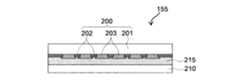
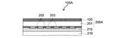
図22A乃至図22Cに示すように、静電容量方式のタッチパネルセンサ110は、タッチパネルセンサ用基板116と、タッチパネルセンサ用基板116の観察者側の面上に所定のパターンで設けられた複数のx透明導電パターン111およびy透明導電パターン112とを有している。図22Aに示すように、x透明導電パターン111はx方向に延びており、またy透明導電パターン112はx方向に直交するy方向に延びている。  22A to 22C, the capacitivetouch panel sensor 110 includes a touchpanel sensor substrate 116 and a plurality of x provided in a predetermined pattern on the viewer side surface of the touchpanel sensor substrate 116. The transparentconductive pattern 111 and the y transparentconductive pattern 112 are provided. As shown in FIG. 22A, the x transparentconductive pattern 111 extends in the x direction, and the y transparentconductive pattern 112 extends in the y direction orthogonal to the x direction.

各x透明導電パターン111は、略正方形の形状を有する複数のx電極単位111aと、隣接するx電極単位111a間をx方向において接続するx接続部111bと、を有している。このようなx透明導電パターン111により、被検出体のタッチ箇所のy方向における位置が検出される。また、各y透明導電パターン112は、略正方形の形状を有する複数のy電極単位112aと、隣接するy電極単位112a間をy方向において接続するy接続部112bと、を有している。このようなy透明導電パターン112により、被検出体のタッチ箇所のx方向における位置が検出される。  Each x transparentconductive pattern 111 has a plurality ofx electrode units 111a having a substantially square shape, and anx connection part 111b that connects adjacentx electrode units 111a in the x direction. By such an x transparentconductive pattern 111, the position in the y direction of the touch location of the detection object is detected. Each of the y transparentconductive patterns 112 includes a plurality ofy electrode units 112a having a substantially square shape, anda y connection portion 112b that connects adjacenty electrode units 112a in the y direction. Such a y transparentconductive pattern 112 detects the position in the x direction of the touch location of the detection object.

またタッチパネルセンサ用基板116上には、所定のパターンで設けられ、x透明導電パターン111およびy透明導電パターン112にそれぞれ電気的に接続された取出配線113および取出配線114と、取出配線113および取出配線114に接続され、x透明導電パターン111およびy透明導電パターン112からの信号を外部へ取り出すための端子部115と、が設けられている。  Further, on the touchpanel sensor substrate 116, theextraction wiring 113 and theextraction wiring 114, which are provided in a predetermined pattern and are electrically connected to the x transparentconductive pattern 111 and the y transparentconductive pattern 112, respectively, and theextraction wiring 113 and the extraction wiring.Terminal portions 115 connected to thewiring 114 and for taking out signals from the x transparentconductive pattern 111 and the y transparentconductive pattern 112 to the outside are provided.

タッチパネルセンサ110においては、上述の各導電パターン111,112、取出配線113,114および端子部115の組合体により、タッチ位置を検出するとともに検出信号を外部へ取り出すというタッチパネル機能を実現するセンサ部120が構成されている。  In thetouch panel sensor 110, asensor unit 120 that realizes a touch panel function of detecting a touch position and extracting a detection signal to the outside by a combination of theconductive patterns 111 and 112, theextraction wirings 113 and 114, and theterminal unit 115 described above. Is configured.

次に、タッチパネルセンサ110の各構成要素の材料について説明する。各x透明導電パターン111およびy透明導電パターン112は、映像を表示させるための表示領域に配置される。このため各x透明導電パターン111およびy透明導電パターン112は、導電性および透明性を有する材料、例えばITOなどから構成される。一方、取出配線113、取出配線114および端子部115は、表示領域の周縁に位置する非表示領域に配置される。このため、取出配線113、取出配線114および端子部115を構成する材料が透明性を有する必要はない。従って取出配線113、取出配線114および端子部115は一般に、x透明導電パターン111およびy透明導電パターン112の材料よりも高い電気伝導率を有する金属材料から構成される。  Next, the material of each component of thetouch panel sensor 110 will be described. Each of the x transparentconductive pattern 111 and the y transparentconductive pattern 112 is disposed in a display area for displaying an image. Therefore, each of the x transparentconductive pattern 111 and the y transparentconductive pattern 112 is made of a material having conductivity and transparency, such as ITO. On the other hand, theextraction wiring 113, theextraction wiring 114, and theterminal portion 115 are arranged in a non-display area located at the periphery of the display area. For this reason, the material which comprises theextraction wiring 113, theextraction wiring 114, and theterminal part 115 does not need to have transparency. Therefore, the lead-outwiring 113, the lead-outwiring 114, and theterminal portion 115 are generally made of a metal material having a higher electrical conductivity than the materials of the x transparentconductive pattern 111 and the y transparentconductive pattern 112.

タッチパネルセンサ用基板116の材料は、各導電パターン111,112、取出配線113,114および端子部115を支持するとともに、透明性を有する限り特に限定されない。例えばタッチパネルセンサ用基板116の材料として、透明性を有するガラスやポリマーなどが用いられる。  The material of the touchpanel sensor substrate 116 is not particularly limited as long as it supports theconductive patterns 111 and 112, theextraction wirings 113 and 114, and theterminal portion 115 and has transparency. For example, glass or polymer having transparency is used as the material for the touchpanel sensor substrate 116.

図22Bおよび図22Cに示すように、各導電パターン111,112、取出配線113,114および端子部115を含むセンサ部120は、タッチパネルセンサ用基板116上にITOや金属材料などを積層させることにより形成される。なお図22Bおよび図22Cに示すように、x接続部111bとy接続部112bとが電気的に接続されることを防ぐため、x接続部111bとy接続部112bとの間に絶縁層117が介在されていてもよい。また、図22Bおよび図22Cにおいて一点鎖線で示されているように、各導電パターン111,112、取出配線113,114および端子部115を保護するための保護層119が設けられていてもよい。保護層119としては、透明性および絶縁性を有する樹脂材料などが適宜用いられる。  As shown in FIGS. 22B and 22C, thesensor unit 120 including theconductive patterns 111 and 112, theextraction wirings 113 and 114 and theterminal unit 115 is formed by laminating ITO or a metal material on the touchpanel sensor substrate 116. It is formed. As shown in FIGS. 22B and 22C, an insulatinglayer 117 is provided between thex connection portion 111b and they connection portion 112b in order to prevent thex connection portion 111b and they connection portion 112b from being electrically connected. It may be interposed. 22B and 22C, aprotective layer 119 for protecting theconductive patterns 111 and 112, theextraction wirings 113 and 114, and theterminal portion 115 may be provided. As theprotective layer 119, a resin material having transparency and insulation is used as appropriate.

本実施の形態によれば、表示装置の表示部50がタッチパネルセンサ110を有している。このため、表示装置にタッチパネル機能を付与することができる。また表示部50のタッチパネルセンサ110の観察者側には、上述の第1乃至第6の形態による表示用前面板40が設けられている。このため、表示用前面板40によってタッチパネルセンサ110を適切に保護することができ、かつ、表示装置の観察者側において外光の反射が生じるのを防ぐことができる。  According to the present embodiment, thedisplay unit 50 of the display device has thetouch panel sensor 110. For this reason, a touch panel function can be provided to the display device. Further, thedisplay front plate 40 according to the first to sixth embodiments described above is provided on the viewer side of thetouch panel sensor 110 of thedisplay unit 50. For this reason, thetouch panel sensor 110 can be appropriately protected by thedisplay front plate 40, and reflection of external light on the viewer side of the display device can be prevented.

なお上述の例においては、センサ部120がタッチパネルセンサ用基板116の観察者側の面上に設けられている例を示した。しかしながら、これに限られることはなく、センサ部120がタッチパネルセンサ用基板116の表示部側の面上に設けられていてもよい。
また、センサ部120の各構成要素の一部分がタッチパネルセンサ用基板116の観察者側の面上に設けられ、センサ部120の各構成要素のその他の部分がタッチパネルセンサ用基板116の表示部側の面上に設けられていてもよい。例えば、x透明導電パターン111がタッチパネルセンサ用基板116の観察者側の面上に設けられ、y透明導電パターン112がタッチパネルセンサ用基板116の表示部側の面上に設けられていてもよい。
In the above-described example, the example in which thesensor unit 120 is provided on the surface on the viewer side of the touchpanel sensor substrate 116 is shown. However, the present invention is not limited to this, and thesensor unit 120 may be provided on the display unit side surface of the touchpanel sensor substrate 116.
In addition, a part of each component of thesensor unit 120 is provided on the surface of the touchpanel sensor substrate 116 on the viewer side, and the other part of each component of thesensor unit 120 is on the display unit side of the touchpanel sensor substrate 116. It may be provided on the surface. For example, the x transparentconductive pattern 111 may be provided on the surface of the touchpanel sensor substrate 116 on the viewer side, and the y transparentconductive pattern 112 may be provided on the surface of the touchpanel sensor substrate 116 on the display unit side.

(変形例)
図23に示すように、タッチパネルセンサ110は、タッチパネルセンサ用基板116およびセンサ部120に加えて、センサ部120により検出された信号を処理するための信号処理部125をさらに有していてもよい。信号処理部125は、例えば、プリント基板と、プリント基板上に設けられ、センサ部120からの信号に基づいてタッチ箇所を解析する処理用ICとを含んでいる。また、電気信号を外部に取り出すため配線が信号処理部125に含まれていてもよい。このような配線は、例えばフレキシブル基板から構成されていてもよい。
信号処理部125は、例えば図22Aにおいて一点鎖線で示されているように、センサ部120の端子部115に接続される。
(Modification)
As shown in FIG. 23, thetouch panel sensor 110 may further include asignal processing unit 125 for processing a signal detected by thesensor unit 120 in addition to the touchpanel sensor substrate 116 and thesensor unit 120. . Thesignal processing unit 125 includes, for example, a printed circuit board and a processing IC that is provided on the printed circuit board and analyzes a touch location based on a signal from thesensor unit 120. In addition, a wiring may be included in thesignal processing unit 125 to extract an electrical signal to the outside. Such wiring may be composed of, for example, a flexible substrate.
Thesignal processing unit 125 is connected to theterminal unit 115 of thesensor unit 120, for example, as indicated by a one-dot chain line in FIG. 22A.

また図24に示すように、タッチパネルセンサ110が信号処理部125をさらに有し、かつ、タッチパネルセンサ110と表示用前面板40との間に接着層101が設けられていてもよい。  As shown in FIG. 24, thetouch panel sensor 110 may further include asignal processing unit 125, and theadhesive layer 101 may be provided between thetouch panel sensor 110 and thedisplay front plate 40.

第7の実施の形態
次に図25乃至図37を参照して、本発明の第7の実施の形態について説明する。本実施の形態においては、上述の各実施の形態における表示装置の表示部がLCDタイプのものである場合の具体的な構成例について説明する。図25乃至図37に示す第7の実施の形態において、上述の各実施の形態と同一部分には同一符号を付して詳細な説明は省略する。
Seventh Embodiment Next, aseventh embodiment of the present invention will be described with reference to FIGS. In the present embodiment, a specific configuration example in the case where the display unit of the display device in each of the above embodiments is an LCD type will be described. In the seventh embodiment shown in FIGS. 25 to 37, the same parts as those in the above-described embodiments are denoted by the same reference numerals, and detailed description thereof is omitted.

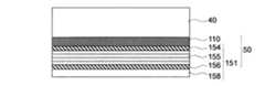
図25は、LCDタイプの表示部50を備えた表示装置の一例を示す図である。図25に示すように、表示部50は、LCDタイプの表示ユニット151と、表示ユニット151の観察者側に設けられたタッチパネルセンサ110とを有している。  FIG. 25 is a diagram illustrating an example of a display device including an LCDtype display unit 50. As shown in FIG. 25, thedisplay unit 50 includes an LCDtype display unit 151 and atouch panel sensor 110 provided on the viewer side of thedisplay unit 151.

(表示ユニット)
表示ユニット151は、バックライトユニット158と、バックライトユニット158の観察者側に設けられた光源側偏光板156と、光源側偏光板156の観察者側に設けられたLCDパネル155と、LCDパネル155の観察者側に設けられた観察者側偏光板154と、を有している。バックライトユニット158としては、蛍光管やLEDなど様々なタイプの光源が用いられ得る。また、蛍光管やLEDなどの外側(観察者側と反対の側)に、蛍光管やLEDなどからの光を反射する反射板がさらに包含されていてもよい。観察者側偏光板154および光源側偏光板156としては、LCDタイプの表示部において周知の偏光板が適宜用いられ得る。なお図示はしないが、表示装置の各構成要素間には接着層が介在されていてもよい。
(Display unit)
Thedisplay unit 151 includes abacklight unit 158, a light sourceside polarizing plate 156 provided on the viewer side of thebacklight unit 158, anLCD panel 155 provided on the viewer side of the light sourceside polarizing plate 156, and an LCD panel And 155 an observerside polarizing plate 154 provided on the observer side. As thebacklight unit 158, various types of light sources such as fluorescent tubes and LEDs can be used. In addition, a reflection plate that reflects light from the fluorescent tube or the LED may be further included outside the fluorescent tube or the LED (on the side opposite to the observer side). As the observer-sidepolarizing plate 154 and the light source-sidepolarizing plate 156, well-known polarizing plates can be appropriately used in the LCD type display unit. Although not shown, an adhesive layer may be interposed between the constituent elements of the display device.

(LCDパネル)
LCDパネル155は、図26に示すように、TFT基板210と、TFT基板210の観察者側に設けられたカラーフィルタ200と、TFT基板210とカラーフィルタ200との間に充填された液晶層215と、を含んでいる。TFT基板210は、図示はしないが、各々が表示装置の単位画素に対応し、液晶215に所定の電圧を印加して液晶層215の状態を制御する複数の液晶駆動部を含んでいる。またカラーフィルタ200は、カラーフィルタ用基板201と、カラーフィルタ用基板201上に所定パターンで設けられたブラックマトリクス層202と、ブラックマトリクス層202間に設けられた複数色の着色層203と、を含んでいる。
(LCD panel)
As shown in FIG. 26, theLCD panel 155 includes aTFT substrate 210, acolor filter 200 provided on the viewer side of theTFT substrate 210, and aliquid crystal layer 215 filled between theTFT substrate 210 and thecolor filter 200. And. Although not shown, each of theTFT substrates 210 corresponds to a unit pixel of the display device, and includes a plurality of liquid crystal driving units that apply a predetermined voltage to theliquid crystal 215 to control the state of theliquid crystal layer 215. Thecolor filter 200 includes acolor filter substrate 201, ablack matrix layer 202 provided in a predetermined pattern on thecolor filter substrate 201, and a plurality ofcolored layers 203 provided between the black matrix layers 202. Contains.

カラーフィルタ用基板201の材料は、ブラックマトリクス層202および着色層203を適切に支持するとともに、透明性を有する限り特に限定されない。例えばカラーフィルタ用基板201の材料として、透明性を有するガラスやポリマーなどが用いられる。  The material of thecolor filter substrate 201 is not particularly limited as long as it appropriately supports theblack matrix layer 202 and thecolored layer 203 and has transparency. For example, as a material for thecolor filter substrate 201, transparent glass, polymer, or the like is used.

本実施の形態によれば、LCDタイプの表示装置は、表示部50と、表示部50の観察者側に設けられた表示用前面板40とを備えている。このため、LCDタイプの表示装置の観察者側において外光の反射が生じるのを防ぐことができる。  According to the present embodiment, the LCD type display device includes thedisplay unit 50 and thedisplay front plate 40 provided on the viewer side of thedisplay unit 50. For this reason, it is possible to prevent external light from being reflected on the viewer side of the LCD type display device.

また本実施の形態によれば、表示部50はタッチパネルセンサ110を有している。このため、LCDタイプの表示装置にタッチパネル機能を付与することができる。  Further, according to the present embodiment, thedisplay unit 50 includes thetouch panel sensor 110. Therefore, a touch panel function can be given to the LCD type display device.

(変形例)
なお本実施の形態において、図27に示すように、表示ユニット151が、光源側偏光板156とバックライトユニット158との間に設けられた光学補償フィルム157をさらに含んでいてもよい。光学補償フィルム157は、例えば、位相差フィルム、輝度向上フィルムまたは導光板などからなっている。このような光学補償フィルム157をさらに設けることにより、バックライトユニット158から光源側偏光板156に入射される光の品質をより高くすることができる。なお光学補償フィルム157は、バックライトユニット158とは別途の構成要素となっていてもよく、または、バックライトユニット158に含まれる構成要素となっていてもよい。
(Modification)
In the present embodiment, as shown in FIG. 27, thedisplay unit 151 may further include anoptical compensation film 157 provided between the light sourceside polarizing plate 156 and thebacklight unit 158. Theoptical compensation film 157 is made of, for example, a retardation film, a brightness enhancement film, a light guide plate, or the like. By further providing such anoptical compensation film 157, the quality of light incident on the light sourceside polarizing plate 156 from thebacklight unit 158 can be further increased. Theoptical compensation film 157 may be a component separate from thebacklight unit 158 or may be a component included in thebacklight unit 158.

(中間製品)
なお上述の本実施の形態およびその変形例において、バックライトユニット158を含む表示ユニット151がタッチパネルセンサ110や表示用前面板40と組み合わされる例を示した。しかしながら、これに限られることはなく、表示ユニット151が形成されるよりも前の段階で、表示ユニット151の各構成要素、例えば観察者側偏光板154やLCDパネル155がタッチパネルセンサ110や表示用前面板40と組み合わされてもよい。
(Intermediate product)
In the above-described embodiment and its modifications, an example in which thedisplay unit 151 including thebacklight unit 158 is combined with thetouch panel sensor 110 and thedisplay front plate 40 has been described. However, the present invention is not limited to this, and before thedisplay unit 151 is formed, each component of thedisplay unit 151, such as the observer-sidepolarizing plate 154 and theLCD panel 155, is thetouch panel sensor 110 and the display unit. It may be combined with thefront plate 40.

例えば図28に示すように、観察者側偏光板154およびLCDパネル155がタッチパネルセンサ110および表示用前面板40と組み合わされ、これによって、表示装置のための中間製品220が構成されてもよい。
また図29に示すように、観察者側偏光板154,LCDパネル155および光源側偏光板156がタッチパネルセンサ110および表示用前面板40と組み合わされ、これによって、表示装置のための中間製品220が構成されてもよい。
また図30に示すように、観察者側偏光板154,LCDパネル155,光源側偏光板156および光学補償フィルム157がタッチパネルセンサ110および表示用前面板40と組み合わされ、これによって、表示装置のための中間製品220が構成されてもよい。
For example, as shown in FIG. 28, the observer-sidepolarizing plate 154 and theLCD panel 155 may be combined with thetouch panel sensor 110 and thedisplay front plate 40, thereby forming anintermediate product 220 for the display device.
Further, as shown in FIG. 29, an observerside polarizing plate 154, anLCD panel 155, and a light sourceside polarizing plate 156 are combined with thetouch panel sensor 110 and thedisplay front plate 40, whereby anintermediate product 220 for a display device is formed. It may be configured.
Further, as shown in FIG. 30, an observer-sidepolarizing plate 154, anLCD panel 155, a light source-sidepolarizing plate 156, and anoptical compensation film 157 are combined with thetouch panel sensor 110 and thedisplay front plate 40, thereby providing a display device.Intermediate product 220 may be configured.

(タッチパネルセンサの配置の変形例)
また上述の本実施の形態およびその変形例において、タッチパネルセンサ110が表示ユニット151とは別個の構成要素となっており、かつ、タッチパネルセンサ110が表示ユニット151のLCDパネル155の観察者側に設けられている例を示した。しかしながら、これに限られることはなく、タッチパネルセンサ110が表示ユニット151に包含され、かつ、タッチパネルセンサ110が観察者側偏光板154とLCDパネル155との間に設けられていてもよい。
(Modification of touch panel sensor arrangement)
In the above-described embodiment and its modifications, thetouch panel sensor 110 is a separate component from thedisplay unit 151, and thetouch panel sensor 110 is provided on the viewer side of theLCD panel 155 of thedisplay unit 151. An example is given. However, the present invention is not limited to this, and thetouch panel sensor 110 may be included in thedisplay unit 151, and thetouch panel sensor 110 may be provided between the observer-sidepolarizing plate 154 and theLCD panel 155.

図31乃至図35は、タッチパネルセンサ110が観察者側偏光板154とLCDパネル155との間に設けられる形態の例を示す図である。図31乃至図35に示す形態はそれぞれ、タッチパネルセンサ110が観察者側偏光板154とLCDパネル155との間に設けられている点が異なるのみであり、他の構成は、図25,図27乃至図30に示す形態と略同一である。  FIG. 31 to FIG. 35 are diagrams showing examples of forms in which thetouch panel sensor 110 is provided between the observer-sidepolarizing plate 154 and theLCD panel 155. The configurations shown in FIGS. 31 to 35 are different from each other only in that thetouch panel sensor 110 is provided between the observer-sidepolarizing plate 154 and theLCD panel 155. Other configurations are the same as those in FIGS. Thru | or substantially the same as the form shown in FIG.

なお「タッチパネルセンサ110が表示ユニット151とは別個の構成要素となっている」とは、タッチパネルセンサ110が表示ユニット151とは別個に取引、搬送などされることを意味している。また、「タッチパネルセンサ110が表示ユニット151に包含されている」とは、タッチパネルセンサ110が表示ユニット151と同時に取引、搬送などされることを意味している。  Note that “thetouch panel sensor 110 is a separate component from thedisplay unit 151” means that thetouch panel sensor 110 is traded, transported, or the like separately from thedisplay unit 151. Further, “thetouch panel sensor 110 is included in thedisplay unit 151” means that thetouch panel sensor 110 is transacted or transported at the same time as thedisplay unit 151.

(タッチパネルセンサ一体型カラーフィルタの例)
また上述の本実施の形態およびその変形例において、タッチパネルセンサ110がLCDパネル155のカラーフィルタ200とは別個の構成要素となっている例を示した。しかしながら、これに限られることはなく、タッチパネルセンサがカラーフィルタ200と一体に形成されていてもよい。なお「タッチパネルセンサがカラーフィルタと一体に形成される」とは、以下に図36を参照して説明するように、タッチパネルセンサ用の基板とカラーフィルタ用の基板とが共通になっていることを意味している。
(Example of touch panel sensor integrated color filter)
Further, in the above-described embodiment and its modification examples, thetouch panel sensor 110 is an example in which thetouch panel sensor 110 is a separate component from thecolor filter 200 of theLCD panel 155. However, the present invention is not limited to this, and the touch panel sensor may be formed integrally with thecolor filter 200. Note that “the touch panel sensor is formed integrally with the color filter” means that the touch panel sensor substrate and the color filter substrate are common, as will be described below with reference to FIG. I mean.

図36は、タッチパネル機能を有するタッチパネルセンサ一体型のカラーフィルタ200Aを示す図である。図36に示すように、カラーフィルタ200Aは、カラーフィルタ用基板201と、カラーフィルタ用基板201の観察側に設けられたセンサ部120と、カラーフィルタ用基板201の表示部側に設けられたブラックマトリクス層202および着色層203と、を有している。ここでセンサ部120は、図20乃至図24に示す第6の実施の形態におけるセンサ部120と略同一であるので、詳細な説明を省略する。  FIG. 36 is a diagram showing acolor filter 200A integrated with a touch panel sensor having a touch panel function. As shown in FIG. 36, thecolor filter 200A includes acolor filter substrate 201, asensor unit 120 provided on the observation side of thecolor filter substrate 201, and a black provided on the display unit side of thecolor filter substrate 201. Amatrix layer 202 and acolored layer 203. Here, thesensor unit 120 is substantially the same as thesensor unit 120 in the sixth embodiment shown in FIGS.

本変形例においては、LCDパネル155Aがタッチパネルセンサ一体型のカラーフィルタ200Aを有することにより、LCDパネル155Aにタッチパネル機能が付与されている。図37は、タッチパネル機能を有するLCDパネル155Aを備えた表示装置を示す図である。  In the present modification, theLCD panel 155A includes the touch panel sensor-integratedcolor filter 200A, so that theLCD panel 155A has a touch panel function. FIG. 37 is a diagram showing a display device including anLCD panel 155A having a touch panel function.

本変形例によれば、上述のように、タッチパネルセンサがカラーフィルタと一体に形成される。これによって、表示装置により簡易にタッチパネル機能を付与することができる。また、カラーフィルタ200とタッチパネルセンサ110とが別体で構成される場合に比べて、タッチパネルセンサ用の基板を不要にすることができる。従って、タッチパネルセンサ一体型のカラーフィルタ200Aを用いてタッチパネル機能付きの表示装置を構成する場合、タッチパネルセンサ用の基板の分だけ表示装置の厚みおよび重量を低減することができる。
なお、カラーフィルタ200とタッチパネルセンサ110とが別体で構成される場合、カラーフィルタ200とタッチパネルセンサ110とが接着層などにより貼り合わされることが考えられる。このため、接着層の分だけタッチパネルセンサ110における光の透過率が低下することが考えらえる。一方、本変形例によれば、タッチパネルセンサとカラーフィルタとを一体に形成することにより、貼り合わせのための接着層が不要となっている。これによって、光の透過率を向上させることができる。また、接着層を用いてカラーフィルタ200とタッチパネルセンサ110とを貼り合わせる工程が不要となる。これによって、製造の工数を削減するとともに、貼り合わせの際に生じうる不具合を回避することができる。例えば、貼り合わせの際に気泡などが混入し、これによって歩留りが低下するというような懸念をなくすことができる。
According to this modification, as described above, the touch panel sensor is formed integrally with the color filter. Thereby, the touch panel function can be easily provided by the display device. Further, a substrate for the touch panel sensor can be made unnecessary as compared with the case where thecolor filter 200 and thetouch panel sensor 110 are configured separately. Therefore, when a display device with a touch panel function is configured using thecolor filter 200A integrated with the touch panel sensor, the thickness and weight of the display device can be reduced by the amount of the substrate for the touch panel sensor.
In addition, when thecolor filter 200 and thetouch panel sensor 110 are comprised separately, it is possible that thecolor filter 200 and thetouch panel sensor 110 are bonded together by an adhesive layer. For this reason, it can be considered that the light transmittance in thetouch panel sensor 110 is reduced by the amount of the adhesive layer. On the other hand, according to this modification, the touch panel sensor and the color filter are integrally formed, thereby eliminating the need for an adhesive layer for bonding. Thereby, the light transmittance can be improved. Moreover, the process of bonding thecolor filter 200 and thetouch panel sensor 110 using an adhesive layer is not necessary. As a result, the number of manufacturing steps can be reduced, and problems that may occur during bonding can be avoided. For example, it is possible to eliminate the concern that bubbles or the like are mixed at the time of bonding, thereby reducing the yield.

なお本明細書において、「表示装置/表示部50/表示ユニット151がタッチパネルセンサ110を備えた/有する/含む」とは、表示装置/表示部50/表示ユニット151が、独立して取引、搬送などされ得るタッチパネルセンサ110を備えた/有する/含む場合だけでなく、カラーフィルタなどの表示装置/表示部50/表示ユニット151の所定の構成要素にセンサ部120が包含されている場合も含む概念となっている。  In this specification, “the display device /display unit 50 /display unit 151 includes / includes / includes thetouch panel sensor 110” means that the display device /display unit 50 /display unit 151 performs transaction and transport independently. Not only including / including / including atouch panel sensor 110 that can be used, but also including a case where thesensor unit 120 is included in a predetermined component of the display device /display unit 50 /display unit 151 such as a color filter. It has become.

第8の実施の形態
次に図38および図39を参照して、本発明の第8の実施の形態について説明する。本実施の形態においては、上述の第1乃至第6の実施の形態における表示装置の表示部が有機ELまたは無機ELタイプのものである場合の具体的な構成例について説明する。図38および図39に示す第8の実施の形態において、上述の各実施の形態と同一部分には同一符号を付して詳細な説明は省略する。
Eighth Embodiment Next, with reference to FIGS. 38 and 39, an eighth embodiment of the present invention will be described. In the present embodiment, a specific configuration example in the case where the display portion of the display device in the first to sixth embodiments is an organic EL or inorganic EL type will be described. In the eighth embodiment shown in FIGS. 38 and 39, the same parts as those in the above-described embodiments are denoted by the same reference numerals, and detailed description thereof is omitted.

図38は、有機ELまたは無機ELタイプの表示部50を備えた表示装置の一例を示す図である。図38に示すように、表示部50は、有機ELまたは無機ELタイプの表示ユニット151と、表示ユニット151の観察者側に設けられたタッチパネルセンサ110とを有している。  FIG. 38 is a diagram illustrating an example of a display device including an organic EL or inorganic ELtype display unit 50. As shown in FIG. 38, thedisplay unit 50 includes an organic EL or inorganic ELtype display unit 151 and atouch panel sensor 110 provided on the viewer side of thedisplay unit 151.

(表示ユニット)
表示ユニット151は、反射電極層164と、反射電極層164の観察者側に設けられ、有機発光材料または無機発光材料からなる発光層163と、発光層163の観察者側に設けられたカラーフィルタ200と、カラーフィルタ200の観察者側に設けられた観察者側偏光板154と、を有している。なお図示はしないが、表示装置の各構成要素間には接着層が介在されていてもよい。
(Display unit)
Thedisplay unit 151 is provided on the viewer side of thereflective electrode layer 164 and thereflective electrode layer 164, alight emitting layer 163 made of an organic light emitting material or an inorganic light emitting material, and a color filter provided on the viewer side of thelight emitting layer 163. 200 and an observer-sidepolarizing plate 154 provided on the observer side of thecolor filter 200. Although not shown, an adhesive layer may be interposed between the constituent elements of the display device.

本実施の形態によれば、有機ELまたは無機ELタイプの表示装置は、表示部50と、表示部50の観察者側に設けられた表示用前面板40とを備えている。このため、有機ELまたは無機ELタイプの表示装置の観察者側において外光の反射が生じるのを防ぐことができる。  According to the present embodiment, the organic EL or inorganic EL type display device includes thedisplay unit 50 and thedisplay front plate 40 provided on the viewer side of thedisplay unit 50. For this reason, it is possible to prevent external light from being reflected on the observer side of the organic EL or inorganic EL type display device.

また本実施の形態によれば、表示部50はタッチパネルセンサ110を有している。このため、有機ELまたは無機ELタイプの表示装置にタッチパネル機能を付与することができる。  Further, according to the present embodiment, thedisplay unit 50 includes thetouch panel sensor 110. For this reason, a touch panel function can be provided to an organic EL or inorganic EL type display device.

(中間製品)
なお上述の本実施の形態において、反射電極層164を含む表示ユニット151がタッチパネルセンサ110や表示用前面板40と組み合わされる例を示した。しかしながら、これに限られることはなく、表示ユニット151が形成されるよりも前の段階で、表示ユニット151の各構成要素、例えば観察者側偏光板154やカラーフィルタ200がタッチパネルセンサ110や表示用前面板40と組み合わされてもよい。
(Intermediate product)
In the above-described embodiment, the example in which thedisplay unit 151 including thereflective electrode layer 164 is combined with thetouch panel sensor 110 and thedisplay front plate 40 has been described. However, the present invention is not limited to this, and before thedisplay unit 151 is formed, each component of thedisplay unit 151, such as the observer-sidepolarizing plate 154 and thecolor filter 200, is thetouch panel sensor 110 and the display unit. It may be combined with thefront plate 40.

例えば図39に示すように、観察者側偏光板154,カラーフィルタ200および発光層163がタッチパネルセンサ110および表示用前面板40と組み合わされ、これによって、表示装置のための中間製品220が構成されてもよい。  For example, as shown in FIG. 39, the observer-sidepolarizing plate 154, thecolor filter 200, and thelight emitting layer 163 are combined with thetouch panel sensor 110 and thedisplay front plate 40, thereby forming anintermediate product 220 for the display device. May be.

また本実施の形態においても、図36および図37に示す形態の場合と同様に、タッチパネル機能を有するタッチパネルセンサ一体型のカラーフィルタ200Aが用いられてもよい。これによって、表示装置により簡易にタッチパネル機能を付与することができる。  Also in the present embodiment, a touch panel sensor integratedcolor filter 200A having a touch panel function may be used as in the case of the embodiments shown in FIGS. Thereby, the touch panel function can be easily provided by the display device.

また本実施の形態においても、図31乃至図35に示す形態の場合と同様に、タッチパネルセンサ110が観察者側偏光板154の表示部側に設けられていてもよい。  Also in the present embodiment, thetouch panel sensor 110 may be provided on the display unit side of the observerside polarizing plate 154 as in the case of the embodiments shown in FIGS.

第9の実施の形態
次に図40乃至図46を参照して、本発明の第9の実施の形態について説明する。図40乃至図46に示す本実施の形態は、表示用前面板がタッチパネルセンサを有する点が異なるのみであり、他の構成は、図1乃至図8に示す第1の実施の形態と略同一である。図40乃至図46に示す第9の実施の形態において、図1乃至図8に示す第1の実施の形態と同一部分には同一符号を付して詳細な説明は省略する。
Ninth Embodiment Next, aninth embodiment of the present invention will be described with reference to FIGS. The present embodiment shown in FIGS. 40 to 46 is different from the first embodiment shown in FIGS. 1 to 8 only in that the display front plate has a touch panel sensor. It is. In the ninth embodiment shown in FIG. 40 to FIG. 46, the same parts as those in the first embodiment shown in FIG. 1 to FIG.

表示用前面板
図40に示すように、表示用前面板40Aは、透明基板20と、透明基板20の観察者側に設けられた反射防止膜30と、透明基板20の表示部側に設けられた意匠層10と、透明基板20および意匠層10の表示部側に設けられたタッチパネルセンサ110と、を有している。このように本実施の形態においては、表示用前面板40Aがタッチパネルセンサ110を有することにより、表示用前面板40Aにタッチパネル機能が付与されている。
Display Front Plate As shown in FIG. 40, thedisplay front plate 40 </ b> A is provided on thetransparent substrate 20, theantireflection film 30 provided on the observer side of thetransparent substrate 20, and the display unit side of thetransparent substrate 20. And thetouch panel sensor 110 provided on the display portion side of thetransparent substrate 20 and thedesign layer 10. As described above, in the present embodiment, thedisplay front plate 40A includes thetouch panel sensor 110, whereby the touch panel function is provided to thedisplay front plate 40A.

なお図40に示す例においては、意匠層10の厚みに起因して、表示領域において、タッチパネルセンサ110が透明基板20に接していないように見える。しかしながら、一般に意匠層10の厚みは1〜10μmの範囲内となっており、一方、タッチパネルセンサ110の厚みは、意匠層10の厚みよりも十分に大きくなっており、例えば数十μm以上となっている。従って、図40に示すように透明基板20および意匠層10の表示部側にタッチパネルセンサ110を設ける場合、タッチパネルセンサ110がたわむことによって、表示領域においてタッチパネルセンサ110が透明基板20に接することになると考えられる。  In the example shown in FIG. 40, due to the thickness of thedesign layer 10, it seems that thetouch panel sensor 110 is not in contact with thetransparent substrate 20 in the display area. However, generally the thickness of thedesign layer 10 is in the range of 1 to 10 μm, while the thickness of thetouch panel sensor 110 is sufficiently larger than the thickness of thedesign layer 10, for example, several tens of μm or more. ing. Therefore, when thetouch panel sensor 110 is provided on the display portion side of thetransparent substrate 20 and thedesign layer 10 as shown in FIG. 40, thetouch panel sensor 110 bends to contact thetransparent substrate 20 in the display area. Conceivable.

図41は、表示部50と、表示部50の観察者側に設けられ、タッチパネルセンサ110を有する表示用前面板40Aと、を備えた表示装置を示す図である。本実施の形態によれば、タッチパネル機能付きの表示用前面板40Aを用いることにより、表示装置にタッチパネル機能をより簡易に付与することができ、かつ、表示装置の観察者側において外光の反射が生じるのを防ぐことができる。  FIG. 41 is a diagram illustrating a display device including thedisplay unit 50 and adisplay front plate 40A provided on the viewer side of thedisplay unit 50 and including thetouch panel sensor 110. According to the present embodiment, by using thedisplay front plate 40A with a touch panel function, the touch panel function can be more easily given to the display device, and the external light is reflected on the viewer side of the display device. Can be prevented.

ところで、図40に示す表示用前面板40Aにおいては、透明基板20に直接的にタッチパネルセンサ110が接している。この場合、透明基板20とタッチパネルセンサ110との間に部分的にエアギャップが生じることが考えられ、このエアギャップに起因して透明基板20の表示部側で光の反射が生じることが考えられる。以下、このような光の反射を防ぐための変形例について説明する。  Meanwhile, in thedisplay front plate 40A shown in FIG. 40, thetouch panel sensor 110 is in direct contact with thetransparent substrate 20. In this case, it is conceivable that an air gap is partially generated between thetransparent substrate 20 and thetouch panel sensor 110, and light is reflected on the display unit side of thetransparent substrate 20 due to the air gap. . Hereinafter, modified examples for preventing such reflection of light will be described.

(第1の変形例)
図42は、透明基板20とタッチパネルセンサ110との間に接着層100が設けられる例を示す図である。このような接着層100を設けることにより、透明基板20とタッチパネルセンサ110との間にエアギャップが生じるのを防ぐことができ、これによって、透明基板20の表示部側において光の反射が生じるのを防ぐことができる。また、意匠層10の厚みに起因して表示領域において生じる透明基板20とタッチパネルセンサ110との間のギャップを接着層100によって埋めることができる。これによって、タッチパネルセンサ110がたわむのを防ぐことができ、このことにより、タッチパネルセンサ110に余計なストレスがかかるのを回避することができる。
(First modification)
FIG. 42 is a diagram illustrating an example in which theadhesive layer 100 is provided between thetransparent substrate 20 and thetouch panel sensor 110. By providing such anadhesive layer 100, it is possible to prevent an air gap from being generated between thetransparent substrate 20 and thetouch panel sensor 110, whereby light is reflected on the display unit side of thetransparent substrate 20. Can be prevented. Further, the gap between thetransparent substrate 20 and thetouch panel sensor 110 generated in the display area due to the thickness of thedesign layer 10 can be filled with theadhesive layer 100. Thereby, it is possible to prevent thetouch panel sensor 110 from being bent, and thereby it is possible to avoid applying extra stress to thetouch panel sensor 110.

なお図42に示す形態においては、接着層100が表示領域および非表示領域の両方に設けられる例を示したが、これに限られることはなく、接着層100が表示領域にのみ設けられていてもよい。これによって、透明基板20の表示部側の表示領域において光の反射が生じるのを防ぐことができる。  42 shows an example in which theadhesive layer 100 is provided in both the display area and the non-display area. However, the present invention is not limited to this, and theadhesive layer 100 is provided only in the display area. Also good. Thereby, it is possible to prevent light from being reflected in the display area on the display unit side of thetransparent substrate 20.

(第2の変形例)
図43は、透明基板20の表示部側に追加反射防止膜35が設けられる例を示す図である。図43に示す形態においては、追加低屈折率層37からなる追加反射防止膜35を設けることにより、透明基板20の表示部側において光の反射が生じるのを防ぐことができる。なお追加反射防止膜35は、耐擦傷性が高められた追加低屈折率層37Aからなっていてもよい。
(Second modification)
FIG. 43 is a diagram illustrating an example in which theadditional antireflection film 35 is provided on the display unit side of thetransparent substrate 20. In the form shown in FIG. 43, by providing theadditional antireflection film 35 made of the additional lowrefractive index layer 37, it is possible to prevent light from being reflected on the display unit side of thetransparent substrate 20. Theadditional antireflection film 35 may be composed of an additional lowrefractive index layer 37A with improved scratch resistance.

(その他の変形例)
なお本実施の形態およびその変形例において、第1の実施の形態による表示用前面板にさらにタッチパネルセンサ110が設けられ、これによってタッチパネル機能付きの表示用前面板40Aが構成される例を示した。しかしながら、これに限られることはなく、図44に示すように、第2の実施の形態による表示用前面板にさらにタッチパネルセンサ110が設けられ、これによってタッチパネル機能付きの表示用前面板40Aが構成されてもよい。図44に示す形態においても、図42および図43に示す形態の場合と同様に、透明基板20とタッチパネルセンサ110との間に接着層100や追加反射防止膜35が設けられていてもよい。
(Other variations)
In the present embodiment and its modifications, an example in which thetouch panel sensor 110 is further provided on the display front plate according to the first embodiment and thedisplay front plate 40A with a touch panel function is configured by this is shown. . However, the present invention is not limited to this, and as shown in FIG. 44, the display front plate according to the second embodiment is further provided with atouch panel sensor 110, thereby forming adisplay front plate 40A with a touch panel function. May be. Also in the form shown in FIG. 44, theadhesive layer 100 and theadditional antireflection film 35 may be provided between thetransparent substrate 20 and thetouch panel sensor 110, similarly to the case shown in FIGS.

また上述の本実施の形態およびその変形例において、反射防止膜30が、非表示領域に位置する部分の全てで除去されている例を示した。しかしながら、これに限られることはなく、反射防止膜30が、非表示領域に位置する部分の一部で除去されていてもよい。  Further, in the above-described embodiment and its modification example, the example in which theantireflection film 30 is removed in all the portions located in the non-display area is shown. However, the present invention is not limited to this, and theantireflection film 30 may be removed at a part of the portion located in the non-display area.

また本実施の形態およびその変形例において、反射防止膜30または追加反射防止膜35が低屈折率層32または追加低屈折率層37,37Aのみからなる形態を示した。しかしながら、これに限られることはなく、反射防止膜30または追加反射防止膜35が高屈折率層をさらに有していてもよい。これによって、反射防止膜30および追加反射防止膜35が外光の反射を防止する効果をより高くすることができる。
また上述の第4の実施の形態の場合と同様に、反射防止膜30の観察者側に接着層100が設けられていてもよい。また上述の第4の実施の形態の変形例の場合と同様に、反射防止膜30の観察者側に設けられた接着層100の観察者側に、飛散防止フィルムからなる保護層105などが設けられていてもよい。これによって、表示用前面板40とその他の部材とを組み合わせる作業を容易化することや、透明基板20が破損してしまった場合に透明基板20の破片が飛散することを防ぐことができる。
Further, in the present embodiment and the modification thereof, the form in which theantireflection film 30 or theadditional antireflection film 35 is composed of only the lowrefractive index layer 32 or the additional low refractive index layers 37 and 37A is shown. However, the present invention is not limited to this, and theantireflection film 30 or theadditional antireflection film 35 may further include a high refractive index layer. Thereby, the effect of preventing reflection of external light by theantireflection film 30 and theadditional antireflection film 35 can be further enhanced.
Further, as in the case of the above-described fourth embodiment, theadhesive layer 100 may be provided on the viewer side of theantireflection film 30. Similarly to the above-described modification of the fourth embodiment, aprotective layer 105 made of a scattering prevention film is provided on the observer side of theadhesive layer 100 provided on the observer side of theantireflection film 30. It may be done. Thereby, it is possible to facilitate the work of combining thedisplay front plate 40 and other members, and to prevent the fragments of thetransparent substrate 20 from scattering when thetransparent substrate 20 is damaged.

また本実施の形態及び変形例において、表示用前面板40Aが、観察者側偏光板154やカラーフィルタ200などをさらに有していてもよい。例えば図45に示すように、透明基板20とタッチパネルセンサ110との間に観察者側偏光板154が設けられていてもよく、また図46に示すように、タッチパネルセンサ110の表示部側にカラーフィルタ200が設けられていてもよい。また、図示はしないが、これらの観察者側偏光板154およびカラーフィルタ200が、図44に示す表示用前面板40Aに設けられていてもよい。また、図示はしないが、図45および図46に示すタッチパネルセンサ110の配置と観察者側偏光板154の配置とが入れ替えられてもよい。  In the present embodiment and the modification, thedisplay front plate 40A may further include an observer-sidepolarizing plate 154, acolor filter 200, and the like. For example, as shown in FIG. 45, an observer-sidepolarizing plate 154 may be provided between thetransparent substrate 20 and thetouch panel sensor 110. Further, as shown in FIG. Afilter 200 may be provided. Further, although not shown, these observer-sidepolarizing plates 154 andcolor filters 200 may be provided on thedisplay front plate 40A shown in FIG. Although not shown, the arrangement of thetouch panel sensor 110 and the arrangement of the observerside polarizing plate 154 shown in FIGS. 45 and 46 may be interchanged.

第10の実施の形態
次に図47乃至図53を参照して、本発明の第10の実施の形態について説明する。図47乃至図53に示す本実施の形態は、タッチパネルセンサが表示用前面板と一体に形成されている点が異なるのみであり、他の構成は、図40乃至図46に示す第9の実施の形態と略同一である。図47乃至図53に示す第10の実施の形態において、図40乃至図46に示す第9の実施の形態と同一部分には同一符号を付して詳細な説明は省略する。
Tenth Embodiment Next, atenth embodiment of the present invention will be described with reference to FIGS. The present embodiment shown in FIGS. 47 to 53 is different only in that the touch panel sensor is formed integrally with the display front plate, and the other configuration is the ninth embodiment shown in FIGS. 40 to 46. The form is substantially the same. In the tenth embodiment shown in FIG. 47 to FIG. 53, the same parts as those in the ninth embodiment shown in FIG. 40 to FIG.

図47は、タッチパネルセンサと一体に形成された表示用前面板40Aを示す図である。図47に示すように、表示用前面板40Aは、透明基板20と、透明基板20の観察者側に設けられた反射防止膜30と、透明基板20の表示部側に設けられた意匠層10と、透明基板20の表示部側の表示領域の面上および意匠層10上に設けられたセンサ部120と、を有している。ここでセンサ部120は、上述の第6の実施の形態において示したセンサ部120と略同一のものである。センサ部120の各構成要素が透明基板20の表示部側の表示領域の面上および意匠層10上にどのように設けられるかについては、特には限定されないが、例えば、センサ部120の透明導電パターン111,112は透明基板20の表示部側の表示領域の面上に形成され、一方、センサ部120の取出配線113,114および端子部115は意匠層10上に形成される。  FIG. 47 is a diagram showing adisplay front plate 40A formed integrally with the touch panel sensor. As shown in FIG. 47, thedisplay front plate 40A includes atransparent substrate 20, anantireflection film 30 provided on the observer side of thetransparent substrate 20, and adesign layer 10 provided on the display unit side of thetransparent substrate 20. And asensor part 120 provided on the surface of the display area on the display part side of thetransparent substrate 20 and on thedesign layer 10. Here, thesensor unit 120 is substantially the same as thesensor unit 120 shown in the above-described sixth embodiment. Although how each component of thesensor unit 120 is provided on the surface of the display area on the display unit side of thetransparent substrate 20 and thedesign layer 10 is not particularly limited, for example, the transparent conductive of thesensor unit 120 Thepatterns 111 and 112 are formed on the surface of the display area on the display part side of thetransparent substrate 20, while theextraction wirings 113 and 114 and theterminal part 115 of thesensor part 120 are formed on thedesign layer 10.

ここで「タッチパネルセンサが表示用前面板40Aと一体に形成される」とは、図47に示されているように、タッチパネルセンサ用の基板と表示用前面板用の透明基板とが共通になっていることを意味している。  Here, "the touch panel sensor is formed integrally with thedisplay front plate 40A" means that the touch panel sensor substrate and the display front plate transparent substrate are common as shown in FIG. It means that

このように本実施の形態によれば、タッチパネルセンサが表示用前面板40Aに一体化されている。これによって、より簡易に表示用前面板40Aにタッチパネル機能を付与することができる。また、タッチパネルセンサ110と表示用前面板40とが別体で構成される場合に比べて、タッチパネルセンサ用の基板を不要にすることができる。従って、表示用前面板40Aを用いてタッチパネル機能付きの表示装置を構成する場合、タッチパネルセンサ用の基板の分だけ表示装置の厚みおよび重量を低減することができる。  Thus, according to the present embodiment, the touch panel sensor is integrated with displayfront plate 40A. Thereby, a touch panel function can be given to thedisplay front plate 40A more easily. Further, the touch panel sensor substrate and thedisplay front plate 40 can be made unnecessary as compared with the case where thetouch panel sensor 110 and thedisplay front plate 40 are configured separately. Therefore, when a display device with a touch panel function is configured using thedisplay front plate 40A, the thickness and weight of the display device can be reduced by the amount of the substrate for the touch panel sensor.

また本実施の形態によれば、透明基板20の表示部側の面がセンサ部120によって覆われている。従って、透明基板20の表示部側の面にエアギャップが形成されることはない。このため、上述の第9の実施の形態の場合のように透明基板20の表示部側に接着層100などを設けることなく、透明基板20の表示部側において光の反射が生じるのを防ぐことができる。すなわち本実施の形態によれば、表示用前面板40Aにタッチパネル機能を付与するだけでなく、同時に、透明基板20の表示部側において光の反射が生じるのを防ぐこともできる。
また、センサ部120と透明基板20との間に接着層100が介在されないようにすることにより、センサ部120の感度を向上させるとともに、光の透過率を向上させることができる。また、接着層100を介して透明基板20とタッチパネルセンサ110とを貼り合わせる工程が不要となり、これによって、製造の工数を削減するとともに、貼り合わせの際に生じうる不具合を回避することができる。例えば、貼り合わせの際に気泡などが混入し、これによって歩留りが低下するというような懸念をなくすことができる。
Further, according to the present embodiment, the surface of thetransparent substrate 20 on the display unit side is covered with thesensor unit 120. Therefore, no air gap is formed on the surface of thetransparent substrate 20 on the display unit side. Therefore, it is possible to prevent light from being reflected on the display unit side of thetransparent substrate 20 without providing theadhesive layer 100 or the like on the display unit side of thetransparent substrate 20 as in the case of the ninth embodiment. Can do. That is, according to the present embodiment, not only a touch panel function can be given to thedisplay front plate 40A, but also light reflection on the display unit side of thetransparent substrate 20 can be prevented.
Further, by preventing theadhesive layer 100 from being interposed between thesensor unit 120 and thetransparent substrate 20, the sensitivity of thesensor unit 120 can be improved and the light transmittance can be improved. Moreover, the process of bonding thetransparent substrate 20 and thetouch panel sensor 110 via theadhesive layer 100 becomes unnecessary, thereby reducing the number of manufacturing steps and avoiding problems that may occur at the time of bonding. For example, it is possible to eliminate the concern that bubbles or the like are mixed at the time of bonding, thereby reducing the yield.

なお本明細書において、「表示用前面板40Aがタッチパネルセンサ110を備えた/有する/含む」とは、表示用前面板40Aが、独立して取引、搬送などされ得るタッチパネルセンサ110を備えた/有する/含む場合だけでなく、表示用前面板40Aの透明基板20上にセンサ部120が形成されている場合も含む概念となっている。  In this specification, “thedisplay front plate 40A includes / includes / includes thetouch panel sensor 110” means that thedisplay front plate 40A includes thetouch panel sensor 110 that can be independently traded, transported, etc. The concept includes not only the case where thesensor unit 120 is included but also the case where thesensor unit 120 is formed on thetransparent substrate 20 of thedisplay front plate 40A.

(変形例)
なおタッチパネルセンサと一体に形成された表示用前面板40Aの形態が図47に示す形態に限られることはなく、その他の様々な形態が考えられ得る。例えば図48に示すように、センサ部120の表示部側に接着層100が設けられていてもよい。また図49および図50に示すように、センサ部120に信号処理部125が取り付けられていてもよい。また図51に示すように、センサ部120の表示部側に観察者側偏光板154が設けられていてもよい。また図52に示すように、観察者側偏光板154の表示部側にカラーフィルタ200がさらに設けられていてもよい。またセンサ部120が透明基板20の表示部側の面上に形成されている例を示したが、これに限られることはなく、センサ部120が透明基板20の観察者側の面上に形成されていてもよい。
(Modification)
The form of thedisplay front plate 40A formed integrally with the touch panel sensor is not limited to the form shown in FIG. 47, and various other forms can be considered. For example, as shown in FIG. 48, theadhesive layer 100 may be provided on the display unit side of thesensor unit 120. Further, as shown in FIGS. 49 and 50, asignal processing unit 125 may be attached to thesensor unit 120. As shown in FIG. 51, an observer-sidepolarizing plate 154 may be provided on the display unit side of thesensor unit 120. As shown in FIG. 52, acolor filter 200 may be further provided on the display unit side of the observerside polarizing plate 154. Moreover, although thesensor part 120 showed the example formed on the surface by the side of the display part of thetransparent substrate 20, it is not restricted to this, Thesensor part 120 is formed on the surface by the side of the observer of thetransparent substrate 20 May be.

(その他の変形例)
なお本実施の形態およびその変形例において、第1の実施の形態による表示用前面板にタッチパネルセンサが一体に形成され、これによってタッチパネル機能付き表示用前面板40Aが得られる例を示した。しかしながら、これに限られることはなく、図53に示すように、第2の実施の形態による表示用前面板にタッチパネルセンサが一体に形成され、これによってタッチパネル機能付き表示用前面板40Aが得られてもよい。図53に示す形態においても、図48乃至図52に示す形態の場合と同様に、接着層100、信号処理部125、観察者側偏光板154およびカラーフィルタ200などが適宜設けられていてもよい。
(Other variations)
In the present embodiment and its modifications, an example is shown in which a touch panel sensor is integrally formed on the display front plate according to the first embodiment, whereby adisplay front plate 40A with a touch panel function is obtained. However, the present invention is not limited to this, and as shown in FIG. 53, the touch panel sensor is integrally formed on the display front plate according to the second embodiment, thereby obtaining thedisplay front plate 40A with a touch panel function. May be. 53, as in the case of the embodiments shown in FIGS. 48 to 52, theadhesive layer 100, thesignal processing unit 125, the observer-sidepolarizing plate 154, thecolor filter 200, and the like may be provided as appropriate. .

また上述の本実施の形態およびその変形例において、反射防止膜30が、非表示領域に位置する部分の全てで除去されている例を示した。しかしながら、これに限られることはなく、反射防止膜30が、非表示領域に位置する部分の一部で除去されていてもよい。  Further, in the above-described embodiment and its modification example, the example in which theantireflection film 30 is removed in all the portions located in the non-display area is shown. However, the present invention is not limited to this, and theantireflection film 30 may be removed at a part of the portion located in the non-display area.

また本実施の形態およびその変形例において、反射防止膜30が低屈折率層32のみからなる形態を示した。しかしながら、これに限られることはなく、反射防止膜30が高屈折率層をさらに有していてもよい。これによって、反射防止膜30が外光の反射を防止する効果をより高くすることができる。また、上述の第3の実施の形態の場合と同様に、表示用前面板40Aが追加反射防止膜35をさらに備えていてもよい。
また上述の第4の実施の形態の場合と同様に、反射防止膜30の観察者側に接着層100が設けられていてもよい。また上述の第4の実施の形態の変形例の場合と同様に、反射防止膜30の観察者側に設けられた接着層100の観察者側に、飛散防止フィルムからなる保護層105などが設けられていてもよい。これによって、表示用前面板40とその他の部材とを組み合わせる作業を容易化することや、透明基板20が破損してしまった場合に透明基板20の破片が飛散することを防ぐことができる。
Further, in the present embodiment and its modifications, theantireflection film 30 is shown as having only the lowrefractive index layer 32. However, the present invention is not limited to this, and theantireflection film 30 may further include a high refractive index layer. Thereby, the effect of theantireflection film 30 preventing reflection of external light can be further enhanced. Further, as in the case of the third embodiment described above, thedisplay front plate 40A may further include anadditional antireflection film 35.
Further, as in the case of the above-described fourth embodiment, theadhesive layer 100 may be provided on the viewer side of theantireflection film 30. Similarly to the above-described modification of the fourth embodiment, aprotective layer 105 made of a scattering prevention film is provided on the observer side of theadhesive layer 100 provided on the observer side of theantireflection film 30. It may be done. Thereby, it is possible to facilitate the work of combining thedisplay front plate 40 and other members, and to prevent the fragments of thetransparent substrate 20 from scattering when thetransparent substrate 20 is damaged.

また本実施の形態の変形例において、タッチパネル機能付きの表示用前面板40Aが観察者側偏光板154やカラーフィルタ200をさらに有する例を示した。しかしながら、これに限られることはなく、タッチパネル機能を有さない表示用前面板40が観察者側偏光板154やカラーフィルタ200をさらに有していてもよい。  In the modification of the present embodiment, an example in which thedisplay front plate 40A with a touch panel function further includes the observer-sidepolarizing plate 154 and thecolor filter 200 has been described. However, the present invention is not limited to this, and thedisplay front plate 40 that does not have a touch panel function may further include the observer-sidepolarizing plate 154 and thecolor filter 200.

また、上記各実施の形態による表示用前面板40,40Aの非表示領域内に形成される意匠層10が、各種のセンサとしての機能を有していてもよい。例えば、意匠層10が光センサとしての機能を有していてもよい。意匠層10が光センサとしての機能を有している場合、意匠層10が、タッチパネルセンサや近接センサなどとして用いられ得るようになる。
近接センサとは、物体が近づいたことを、物体と接触することなく感知することができるセンサである。このような近接センサがスイッチとして用いられる場合、スイッチがあるということが第3者に認識されることなくスイッチとしてのオンオフ切替機能を発揮することが可能となる。例えばタッチパネルセンサ付き携帯電話機等では、人が通話をしようとして耳を携帯電話機等に近づけると、近接センサは、携帯電話機等に耳が近づいたことを感知する。これによって、自動的にタッチパネルディスプレイのオンオフを切り替えることができ、このような仕組みにより、消費電力を節約することができる。また、仮に耳が近づいているときに顔がタッチパネルセンサに接触したとしても、その接触がタッチパネルセンサを用いた操作を目的とするものではないという判断をすることが可能となり、これによって誤動作を防ぐことができる。
近接センサは、近くに物体が存在するかどうかだけでなく、物体までの距離を確認することもできる。このため、例えばデジタルサイネージ用ディスプレイで近接センサが用いられる場合、人が所定の距離まで近づいた場合にのみ電源をオンすることが可能となる。さらに、年齢や性別などを判断するソフトと組み合わせることで、最適な情報を提供することが可能となる。
Moreover, thedesign layer 10 formed in the non-display area of thedisplay front plates 40 and 40A according to the above embodiments may have a function as various sensors. For example, thedesign layer 10 may have a function as an optical sensor. When thedesign layer 10 has a function as an optical sensor, thedesign layer 10 can be used as a touch panel sensor, a proximity sensor, or the like.
The proximity sensor is a sensor that can sense that an object is approaching without contacting the object. When such a proximity sensor is used as a switch, an on / off switching function as a switch can be exhibited without a third person recognizing that there is a switch. For example, in a mobile phone with a touch panel sensor or the like, when a person tries to make a call and an ear is brought close to the mobile phone or the like, the proximity sensor detects that the ear has approached the mobile phone or the like. Accordingly, the touch panel display can be automatically switched on and off, and power consumption can be saved by such a mechanism. In addition, even if the face is in contact with the touch panel sensor when the ear is approaching, it is possible to determine that the contact is not intended for operation using the touch panel sensor, thereby preventing malfunction. be able to.
The proximity sensor can check not only whether there is an object nearby but also the distance to the object. For this reason, for example, when a proximity sensor is used in a digital signage display, the power can be turned on only when a person approaches a predetermined distance. Furthermore, by combining with software that determines age, sex, etc., it is possible to provide optimal information.

(透明基板の変形例)
また上記各実施の形態において、透明基板20としてガラスが用いられる例を示した。しかしながら、これに限られることはなく、透明基板20として、ポリカーボネート、ポリスチレン、アクリルなどのプラスチック基板を用いてもよい。
また、透明基板20としてガラスが用いられる場合、様々なタイプのガラスが用いられ得る。例えば、ソーダガラスやホウケイ酸ガラスなどのアルカリガラスを用いてもよく、または無アルカリガラスを用いてもよい。また、ガラスの表面に化学強化層が設けられた化学強化ガラスが用いられてもよい。ここで化学強化層とは、ガラス中のナトリウムをカリウムに置換することにより形成される層である。このような化学強化層をガラスの表面に形成することにより、透明基板20に何らかの衝撃が加えられた場合に透明基板20が割れてしまうことを抑制することができる。なお、このような化学強化層の厚みが特に限られることはなく、求められる特性に応じて化学強化層の厚みが適宜設定される。例えば、ガラスにある程度の強度を付与しながら、ガラスの切断性および生産性も確保される必要がある場合、化学強化層の厚みが約5〜10μmの範囲内に設定される。また、ガラスにさらに高い強度を付与することが求められる場合、化学強化層の厚みは、約10〜35μmの範囲内に設定されてもよく、35μm以上に設定されてもよい。なお、化学強化層の厚みが約10〜35μmの範囲内となっている場合は、ガラスはある程度の切断性を有している。一方、化学強化層の厚みが35μm以上となっている場合は、仮にダイヤモンドカッターなどの高性能の切断手段が用いられる場合であっても、ガラスを切断することが困難になる。従って、化学強化層の厚みを35μm以上にすることが求められる場合、好ましくは、所望の形状に切り出された後のガラスにイオン交換処理を施すことにより、ガラスの表面に化学強化層が形成される。
このように表面に化学強化層が形成されたガラスの例としては、例えば、コーニング社のGorilla Glass(ゴリラガラス)や、旭硝子社のDragontrail(ドラゴントレイル)などが挙げられる。
(Modified example of transparent substrate)
Moreover, in each said embodiment, the example in which glass is used as thetransparent substrate 20 was shown. However, the present invention is not limited to this, and thetransparent substrate 20 may be a plastic substrate such as polycarbonate, polystyrene, or acrylic.
When glass is used as thetransparent substrate 20, various types of glass can be used. For example, alkali glass such as soda glass or borosilicate glass may be used, or non-alkali glass may be used. Moreover, the chemically strengthened glass with which the chemically strengthened layer was provided in the surface of glass may be used. Here, the chemical strengthening layer is a layer formed by replacing sodium in the glass with potassium. By forming such a chemically strengthened layer on the glass surface, it is possible to prevent thetransparent substrate 20 from cracking when some impact is applied to thetransparent substrate 20. Note that the thickness of such a chemically strengthened layer is not particularly limited, and the thickness of the chemically strengthened layer is appropriately set according to required characteristics. For example, when it is necessary to ensure the cutting property and productivity of the glass while imparting a certain degree of strength to the glass, the thickness of the chemically strengthened layer is set within a range of about 5 to 10 μm. Moreover, when it is calculated | required to give still higher intensity | strength to glass, the thickness of a chemical strengthening layer may be set in the range of about 10-35 micrometers, and may be set to 35 micrometers or more. In addition, when the thickness of the chemical strengthening layer is in the range of about 10 to 35 μm, the glass has a certain degree of cutting ability. On the other hand, when the thickness of the chemically strengthened layer is 35 μm or more, it is difficult to cut the glass even if a high-performance cutting means such as a diamond cutter is used. Therefore, when the thickness of the chemically strengthened layer is required to be 35 μm or more, preferably, the chemically strengthened layer is formed on the surface of the glass by performing ion exchange treatment on the glass after being cut into a desired shape. The
Examples of the glass having a chemically strengthened layer formed on the surface in this way include Corning's Gorilla Glass (Gorilla Glass), Asahi Glass Company's Dragon Trail, and the like.

(低屈折率層の材料の変形例)
また上記各実施の形態において、表示用前面板40のうち観察者側の最表面に位置する層、例えば低屈折率層32や保護層105が、汚れの付着を防止する防汚層としての機能をさらに有していてもよい。防汚層としての機能とは、例えば、人の手が触れることにより付着する油脂成分である指紋に対する耐指紋性、雨水に対する撥水性、汚れの拭取り性に対する滑り性、さらにはマジックを用いた落書きに対する耐マジック性などである。低屈折率層32や保護層105に防汚層としての機能を付与する方法としては、例えば、低屈折率層32や保護層105に所定の割合でケイ素元素、炭素元素およびフッ素元素を含有させることが挙げられる。
(Modification example of material of low refractive index layer)
In each of the above embodiments, the layer located on the outermost surface on the viewer side of thedisplay front plate 40, for example, the lowrefractive index layer 32 or theprotective layer 105 functions as an antifouling layer that prevents the adhesion of dirt. May further be included. The function as an antifouling layer is, for example, the use of fingerprint resistance against fingerprints, which are oils and fats attached when touched by human hands, water repellency against rainwater, slipperiness against dirt wiping, and magic. Magic resistance against graffiti. As a method for imparting a function as an antifouling layer to the lowrefractive index layer 32 or theprotective layer 105, for example, the lowrefractive index layer 32 or theprotective layer 105 contains silicon element, carbon element and fluorine element at a predetermined ratio. Can be mentioned.

(反射防止膜の形成方法の例)
また上記各実施の形態において、反射防止膜30または追加反射防止膜35が、反射防止材料を含む塗布液をダイコート法、スピンコート法またはディップコート法などのウエット法で塗布することにより形成される例を示した。しかしながら、これに限られることはなく、反射防止材料を含む塗布液をインクジェット法により透明基板20上に点状に塗布することにより、反射防止膜30または追加反射防止膜35を形成してもよい。また塗布方法として、グラビア印刷、オフセット印刷、シルクスクリーン印刷などの公知の印刷法が用いられてもよい。これらの塗布方法のうち、好ましくは、上述のようにコストおよび生産性の観点から、ダイコート法、スピンコート法またはディップコート法などのウエット法が採用される。
なお塗布液とは、上述の反射防止材料からなる固形分と、適切な溶媒とを混合することにより構成されるものである。塗布液全体に対する固形分の比率は、塗布方法に応じて適宜設定されるが、好ましくは0.5〜10重量%の範囲内となっており、より好ましくは1〜5重量%の範囲内となっている。
(Example of formation method of antireflection film)
In each of the above embodiments, theantireflection film 30 or theadditional antireflection film 35 is formed by applying a coating solution containing an antireflection material by a wet method such as a die coating method, a spin coating method, or a dip coating method. An example is shown. However, the present invention is not limited to this, and theantireflection film 30 or theadditional antireflection film 35 may be formed by applying a coating liquid containing an antireflection material onto thetransparent substrate 20 in a dot shape by an inkjet method. . As a coating method, a known printing method such as gravure printing, offset printing, silk screen printing, or the like may be used. Among these coating methods, a wet method such as a die coating method, a spin coating method, or a dip coating method is preferably employed from the viewpoint of cost and productivity as described above.
In addition, a coating liquid is comprised by mixing solid content which consists of the above-mentioned antireflection material, and a suitable solvent. The ratio of the solid content with respect to the entire coating solution is appropriately set according to the coating method, but is preferably in the range of 0.5 to 10% by weight, more preferably in the range of 1 to 5% by weight. It has become.

また上記各実施の形態において、ローラ、粘着膜を有するテープ、スキージ、ワイプなどを用いることによって、反射防止膜30または追加反射防止膜35が、非表示領域に位置する部分の全てまたは一部で除去される例を示した。しかしながら、これに限られることはなく、反射防止材料に光硬化樹脂が含まれている場合には、フォトリソグラフィー法を用いることにより、反射防止膜30または追加反射防止膜35が、非表示領域に位置する部分の全てまたは一部で除去されてもよい。
例えば、フォトリソグラフィー用の反射防止材料として光硬化樹脂を用い、かつ酸基を導入した樹脂を用いることによって、露光されていない部分をアルカリ溶液により現像することが可能となる。光硬化樹脂タイプの材料としては、ラジカル系硬化系やカチオン系硬化系の材料が用いられる。ラジカル系硬化系の材料には、アクリル系、エン/チオール系、ビニルエーテル系の材料などが含まれ、カチオン系硬化系の材料には、エポキシ系、オキセタン系、ビニルエーテル系の材料などが含まれる。
また、フォトリソグラフィー法を用いて反射防止膜30または追加反射防止膜35のうち非表示領域に位置する部分の全てまたは一部を除去する際、同時に、反射防止膜30または追加反射防止膜35のその他の部分に対するパターニングが実施されてもよい。すなわち、露光の際に用いられるマスクが、反射防止膜30または追加反射防止膜35のうち非表示領域に位置する部分の全てまたは一部を除去するのに適したパターンを有するだけでなく、反射防止膜30または追加反射防止膜35のその他の部分に対するパターニング性を実現することができるパターンをさらに有していてもよい。これによって、反射防止膜30または追加反射防止膜35に所定のパターンを付与することが可能となる。
In each of the above embodiments, by using a roller, a tape having an adhesive film, a squeegee, a wipe, or the like, theantireflection film 30 or theadditional antireflection film 35 is formed in all or a part of the portion located in the non-display area. An example to be removed is shown. However, the present invention is not limited to this, and when the antireflection material contains a photocurable resin, theantireflection film 30 or theadditional antireflection film 35 is formed in the non-display region by using a photolithography method. It may be removed in all or part of the located part.
For example, by using a photo-curing resin as an antireflection material for photolithography and using a resin into which an acid group is introduced, an unexposed portion can be developed with an alkaline solution. As the photo-curing resin type material, a radical curing material or a cationic curing material is used. The radical curable materials include acrylic, ene / thiol, and vinyl ether materials, and the cationic curable materials include epoxy, oxetane, and vinyl ether materials.
Further, when all or part of the portion of theantireflection film 30 or theadditional antireflection film 35 located in the non-display area is removed by photolithography, theantireflection film 30 or theadditional antireflection film 35 is simultaneously removed. Patterning for other portions may be performed. That is, the mask used at the time of exposure not only has a pattern suitable for removing all or a part of theantireflection film 30 or theadditional antireflection film 35 located in the non-display area, but also a reflection. You may further have the pattern which can implement | achieve the patternability with respect to the other part of theprevention film 30 or theadditional antireflection film 35. FIG. As a result, a predetermined pattern can be applied to theantireflection film 30 or theadditional antireflection film 35.

10 意匠層
20 透明基板
30 反射防止膜
31 盛り上がり部
32 低屈折率層
35 追加反射防止膜
37 追加低屈折率層
40 表示用前面板
40A タッチパネル機能付き表示用前面板
50 表示部
100 接着層
101 接着層
105 保護層
110 タッチパネルセンサ
111 x透明導電パターン
111a x電極単位
111b x接続部
112 y透明導電パターン
112a x電極単位
112b x接続部
113 取出配線
114 取出配線
115 端子部
116 タッチパネルセンサ用基板
117 絶縁層
119 保護層
120 センサ部
125 信号処理部
151 表示ユニット
152 液晶ユニット
154 観察者側偏光板
155 LCDパネル
155A タッチパネル機能付きLCDパネル
156 光源側偏光板
157 光学補償フィルム
158 バックライトユニット
163 発光層
164 反射電極層
200 カラーフィルタ
200A タッチパネルセンサ一体型カラーフィルタ
201 カラーフィルタ用基板
202 ブラックマトリクス層
203 着色層
210 TFT基板
215 液晶層
220 中間製品
DESCRIPTION OFSYMBOLS 10Design layer 20Transparent substrate 30Antireflection film 31 Swellingpart 32 Lowrefractive index layer 35 Additionalantireflective film 37 Additional lowrefractive index layer 40Display front board 40A Display front board with atouch panel function 50Display part 100Adhesive layer 101Adhesion Layer 105protective layer 110 touch panel sensor 111 x transparentconductive pattern 111ax electrode unit 111b x connecting part 112 y transparentconductive pattern 112ax electrode unit 112b x connectingpart 113lead wire 114lead wire 115terminal part 116 touchpanel sensor substrate 117 insulatinglayer 119Protective layer 120Sensor unit 125Signal processing unit 151 Display unit 152Liquid crystal unit 154 Observerside polarizing plate 155LCD panel155A LCD panel 156 with touch panel function Light sourceside polarizing plate 157Optical compensation film 158Backlight unit DOO 163 emittinglayer 164reflective electrode layer 200color filter 200A touch sensor integratedtype color filter 201 for a color filter substrate 202 a black matrix layer 203 acolored layer 210TFT substrate 215liquid crystal layer 220 intermediate products

Claims (36)

Translated fromJapanese
表示部に対して観察者側に配置され、表示領域と非表示領域とを有する表示用前面板において、
透明基板と、
前記透明基板の観察者側に反射防止材料を含む塗布液が塗布されることで設けられた反射防止膜と、
前記透明基板の前記表示部側または観察者側に設けられて前記非表示領域を形成する意匠層と、を備え、
前記反射防止膜は、前記非表示領域に位置した周縁部の少なくとも一部で除去されていることを特徴とする表示用前面板。
In the display front plate that is arranged on the viewer side with respect to the display unit and has a display area and a non-display area,
A transparent substrate;
An antireflection film provided by applying a coating liquid containing an antireflection material on the observer side of the transparent substrate;
A design layer provided on the display unit side or the viewer side of the transparent substrate to form the non-display region, and
The display front plate, wherein the antireflection film is removed at least at a part of a peripheral edge located in the non-display area.
前記透明基板は略矩形状からなり、
前記透明基板の一辺に対応する位置と該一辺に対向する他辺に対応する位置において、前記反射防止膜は除去されていることを特徴とする請求項1に記載の表示用前面板。
The transparent substrate has a substantially rectangular shape,
The display front plate according to claim 1, wherein the antireflection film is removed at a position corresponding to one side of the transparent substrate and a position corresponding to the other side opposite to the one side.
前記反射防止膜は、前記透明基板の一辺に対応する位置と該一辺に対向する他辺に対応する位置において、前記非表示領域に位置する部分の全てが除去されることを請求項2に記載の特徴とする表示用前面板。  3. The antireflection film according to claim 2, wherein all of the portions located in the non-display area are removed at a position corresponding to one side of the transparent substrate and a position corresponding to the other side opposite to the one side. A display front plate characterized by 前記反射防止膜は、周縁部の全周にわたって除去されていることを特徴とする請求項1に記載の表示用前面板。  The display front plate according to claim 1, wherein the antireflection film is removed over the entire periphery. 前記反射防止膜は、前記非表示領域に位置する部分の全てが除去されることを特徴とする請求項4に記載の表示用前面板。  5. The display front plate according to claim 4, wherein the antireflection film is entirely removed from the portion located in the non-display area. 前記非表示領域は、幅が2.0mm以上からなり、
前記反射防止膜は、幅が0.5mm〜2.0mmで除去されていることを特徴とする請求項1、2または4のいずれか1項に記載の表示用前面板。
The non-display area has a width of 2.0 mm or more,
The display front plate according to claim 1, wherein the antireflection film has a width of 0.5 mm to 2.0 mm and is removed.
前記塗布液は、ダイコート法、スピンコート法またはディップコート法によって塗布されることを特徴とする請求項1乃至6のいずれか1項に記載の表示用前面板。  The display front plate according to claim 1, wherein the coating liquid is applied by a die coating method, a spin coating method, or a dip coating method. 前記反射防止膜は、観察者側の最表面に位置する低屈折率層を有し、
前記低屈折率層の光屈折率は前記透明基板の光屈折率よりも小さく、かつ、前記低屈折率層の厚みは80〜150nmの範囲内となっていることを特徴とする請求項1乃至7のいずれかに記載の表示用前面板。
The antireflection film has a low refractive index layer located on the outermost surface on the viewer side,
The light refractive index of the low refractive index layer is smaller than the light refractive index of the transparent substrate, and the thickness of the low refractive index layer is in the range of 80 to 150 nm. The display front plate according to any one of 7.
前記低屈折率層の光屈折率は、1.35よりも小さくなっていることを特徴とする請求項8に記載の表示用前面板。  The display front plate according to claim 8, wherein the light refractive index of the low refractive index layer is smaller than 1.35. 前記透明基板の表示部側に設けられた追加反射防止膜をさらに備え、
前記追加反射防止膜は、表示部側の最表面に位置する追加低屈折率層を有し、
前記追加低屈折率層の光屈折率は前記透明基板の光屈折率よりも小さく、かつ前記追加低屈折率層の厚みは80〜150nmの範囲内となっていることを特徴とする請求項8または9に記載の表示用前面板。
Further comprising an additional antireflection film provided on the display portion side of the transparent substrate,
The additional antireflection film has an additional low refractive index layer located on the outermost surface on the display unit side,
The optical refractive index of the additional low refractive index layer is smaller than the optical refractive index of the transparent substrate, and the thickness of the additional low refractive index layer is in the range of 80 to 150 nm. Or the display front plate according to 9.
前記追加反射防止膜の前記追加低屈折率層の光屈折率は、前記反射防止膜の前記低屈折率層の光屈折率よりも大きくなっていることを特徴とする請求項10に記載の表示用前面板。  The display according to claim 10, wherein the light refractive index of the additional low refractive index layer of the additional antireflection film is larger than the light refractive index of the low refractive index layer of the antireflection film. Front plate. センサ部を含むタッチパネルセンサをさらに備えたことを特徴とする請求項1乃至11のいずれか1項に記載の表示用前面板。  The display front plate according to claim 1, further comprising a touch panel sensor including a sensor unit. 前記センサ部が前記透明基板の観察者側の面上または表示部側の面上に形成されていることを特徴とする請求項12に記載の表示用前面板。  The display front plate according to claim 12, wherein the sensor unit is formed on a surface of the transparent substrate on an observer side or a surface on the display unit side. 前記センサ部に信号処理部が接続されていることを特徴とする請求項12または13に記載の表示用前面板。  The display front plate according to claim 12 or 13, wherein a signal processing unit is connected to the sensor unit. 前記透明基板よりも表示部側に位置する偏光板をさらに備えたことを特徴とする請求項1乃至14のいずれか1項に記載の表示用前面板。  The display front plate according to claim 1, further comprising a polarizing plate positioned closer to the display unit than the transparent substrate. 前記透明基板よりも表示部側に位置するカラーフィルタをさらに備えたことを特徴とする請求項1乃至15のいずれか1項に記載の表示用前面板。  The display front plate according to claim 1, further comprising a color filter positioned closer to the display unit than the transparent substrate. 前記反射防止膜の観察者側に設けられた観察者側接着層をさらに備えたことを特徴とする請求項1乃至16のいずれか1項に記載の表示用前面板。  The display front plate according to claim 1, further comprising an observer-side adhesive layer provided on the observer side of the antireflection film. 前記観察者側接着層の観察者側に設けられた保護層をさらに備えたことを特徴とする請求項17に記載の表示用前面板。  The display front plate according to claim 17, further comprising a protective layer provided on an observer side of the observer-side adhesive layer. 表示部側の最表面に位置する表示部側接着層をさらに備えたことを特徴とする請求項1乃至18のいずれか1項に記載の表示用前面板。  The display front plate according to any one of claims 1 to 18, further comprising a display unit side adhesive layer positioned on an outermost surface on the display unit side. 表示部に対して観察者側に配置され、表示領域と非表示領域とを有する表示用前面板の製造方法において、
透明基板を準備する工程と、
前記透明基板の前記表示部側または観察者側に意匠層を形成する工程と、
前記透明基板の観察者側に反射防止材料を含む塗布液を塗布して、反射防止膜を形成する工程と、
前記反射防止膜を、前記非表示領域に位置した周縁部の少なくとも一部で除去する工程と、
を備えたことを特徴とする表示用前面板の製造方法。
In the manufacturing method of the display front plate, which is arranged on the viewer side with respect to the display unit and has a display area and a non-display area,
Preparing a transparent substrate;
Forming a design layer on the display unit side or the viewer side of the transparent substrate;
Applying a coating liquid containing an antireflection material on the observer side of the transparent substrate to form an antireflection film;
Removing the antireflection film at least at a part of the peripheral edge located in the non-display area;
A method for manufacturing a display front plate, comprising:
前記透明基板は略矩形状からなり、
前記反射防止膜を、前記透明基板の一辺に対応する位置と該一辺に対向する他辺に対応する位置において除去することを特徴とする請求項20に記載の表示用前面板の製造方法。
The transparent substrate has a substantially rectangular shape,
21. The method for manufacturing a display front plate according to claim 20, wherein the antireflection film is removed at a position corresponding to one side of the transparent substrate and a position corresponding to the other side opposite to the one side.
前記反射防止膜を、前記透明基板の一辺に対応する位置と該一辺に対向する他辺に対応する位置において、前記非表示領域に位置する部分の全てで除去することを特徴とする請求項21に記載の表示用前面板の製造方法。  The antireflection film is removed at all of the portions located in the non-display area at a position corresponding to one side of the transparent substrate and a position corresponding to the other side opposite to the one side. The manufacturing method of the front plate for a display of description. 前記反射防止膜を、周縁部の全周にわたって除去することを特徴とする請求項20に記載の表示用前面板の製造方法。  21. The method for manufacturing a display front plate according to claim 20, wherein the antireflection film is removed over the entire periphery of the peripheral portion. 前記反射防止膜を、前記非表示領域に位置する部分の全てで除去することを特徴とする請求項23に記載の表示用前面板の製造方法。  24. The method of manufacturing a display front plate according to claim 23, wherein the antireflection film is removed at all of the portions located in the non-display area. 前記非表示領域は、幅が2.0mm以上からなり、
前記反射防止膜を、幅が0.5mm〜2.0mmで除去することを特徴とする請求項20、21または23のいずれか1項に記載の表示用前面板の製造方法。
The non-display area has a width of 2.0 mm or more,
24. The method for manufacturing a display front plate according to claim 20, wherein the antireflection film is removed with a width of 0.5 mm to 2.0 mm.
前記塗布液は、ダイコート法、スピンコート法またはディップコート法によって塗布されることを特徴とする請求項20乃至25のいずれか1項に記載の表示用前面板の製造方法。  26. The method for manufacturing a display front plate according to claim 20, wherein the coating liquid is applied by a die coating method, a spin coating method, or a dip coating method. 前記反射防止膜の周縁部を、多孔性のローラによって除去することを特徴とする請求項20乃至26のいずれか1項に記載の表示用前面板の製造方法。  27. The method for manufacturing a display front plate according to claim 20, wherein a peripheral edge portion of the antireflection film is removed by a porous roller. 前記反射防止膜の周縁部を、溶剤とアルカリ性の薬液、溶剤と酸性の薬液、または、水を用いて除去することを特徴とする請求項27に記載の表示用前面板の製造方法。  28. The method for manufacturing a display front plate according to claim 27, wherein a peripheral portion of the antireflection film is removed using a solvent and an alkaline chemical, a solvent and an acidic chemical, or water. 前記反射防止膜の周縁部を、粘着膜を有するテープによって除去することを特徴とする請求項20乃至26のいずれか1項に記載の表示用前面板の製造方法。  27. The method for manufacturing a display front plate according to claim 20, wherein a peripheral portion of the antireflection film is removed with a tape having an adhesive film. 表示部と、
前記表示部に対して観察者側に配置され、表示領域と非表示領域とを有する表示用前面板と、を備え、
表示用前面板は、
透明基板と、
前記透明基板の観察者側に反射防止材料を含む塗布液が塗布されることで設けられた反射防止膜と、
前記透明基板の前記表示部側または観察者側に設けられて前記非表示領域を形成する意匠層と、を有し、
前記反射防止膜は、前記非表示領域に位置した周縁部の少なくとも一部で除去されていることを特徴とする表示装置。
A display unit;
A display front plate that is disposed on the viewer side with respect to the display unit and has a display area and a non-display area;
The display front plate
A transparent substrate;
An antireflection film provided by applying a coating liquid containing an antireflection material on the observer side of the transparent substrate;
A design layer provided on the display unit side or the viewer side of the transparent substrate to form the non-display region,
The display device according to claim 1, wherein the antireflection film is removed at at least a part of a peripheral portion located in the non-display area.
前記表示部が、センサ部を含むタッチパネルセンサを有することを特徴とする請求項30に記載の表示装置。  The display device according to claim 30, wherein the display unit includes a touch panel sensor including a sensor unit. 前記表示部が、カラーフィルタをさらに有することを特徴とする請求項31に記載の表示装置。  32. The display device according to claim 31, wherein the display unit further includes a color filter. 前記タッチパネルセンサが、前記カラーフィルタと一体に形成されていることを特徴とする請求項32に記載の表示装置。  The display device according to claim 32, wherein the touch panel sensor is formed integrally with the color filter. 前記表示用前面板が、センサ部を含むタッチパネルセンサを有することを特徴とする請求項30に記載の表示装置。  The display device according to claim 30, wherein the display front plate includes a touch panel sensor including a sensor unit. 前記センサ部が前記表示用前面板の前記透明基板の観察者側の面上または表示部側の面上に形成されていることを特徴とする請求項34に記載の表示装置。  35. The display device according to claim 34, wherein the sensor unit is formed on an observer side surface or a display unit side surface of the transparent substrate of the display front plate. 表示部を準備する工程と、
表示領域と非表示領域とを有する表示用前面板を製造する工程と、
前記表示用前面板を前記表示部の観察者側に配置して取り付ける工程と、を備え、
前記表示用前面板を製造する工程は、
透明基板を準備する工程と、
前記透明基板の前記表示部側または観察者側に意匠層を形成する工程と、
前記透明基板の観察者側に反射防止材料を含む塗布液を塗布して、反射防止膜を形成する工程と、
前記反射防止膜を、前記非表示領域に位置した周縁部の少なくとも一部で除去する工程と、
を有することを特徴とする表示装置の製造方法。
Preparing a display unit;
Producing a display front plate having a display area and a non-display area;
Arranging and attaching the display front plate on the viewer side of the display unit,
The step of manufacturing the display front plate includes:
Preparing a transparent substrate;
Forming a design layer on the display unit side or the viewer side of the transparent substrate;
Applying a coating liquid containing an antireflection material on the observer side of the transparent substrate to form an antireflection film;
Removing the antireflection film at least at a part of the peripheral edge located in the non-display area;
A method for manufacturing a display device, comprising:
JP2011087196A2010-09-212011-04-11 Display front plate, display front plate manufacturing method, display device, and display device manufacturing methodActiveJP5978561B2 (en)

Priority Applications (1)

Application NumberPriority DateFiling DateTitle
JP2011087196AJP5978561B2 (en)2010-09-212011-04-11 Display front plate, display front plate manufacturing method, display device, and display device manufacturing method

Applications Claiming Priority (3)

Application NumberPriority DateFiling DateTitle
JP20102111532010-09-21
JP2011087196AJP5978561B2 (en)2010-09-212011-04-11 Display front plate, display front plate manufacturing method, display device, and display device manufacturing method

Publications (2)

Publication NumberPublication Date
JP2012088684Atrue JP2012088684A (en)2012-05-10
JP5978561B2 JP5978561B2 (en)2016-08-24

Family

ID=46260326

Family Applications (1)

Application NumberTitlePriority DateFiling Date
JP2011087196AActiveJP5978561B2 (en)2010-09-212011-04-11 Display front plate, display front plate manufacturing method, display device, and display device manufacturing method

Country Status (1)

CountryLink
JP (1)JP5978561B2 (en)

Cited By (10)

* Cited by examiner, † Cited by third party
Publication numberPriority datePublication dateAssigneeTitle
JP2016161761A (en)*2015-03-022016-09-05日本精機株式会社Display device
JP2016206867A (en)*2015-04-212016-12-08三菱電機株式会社Touch screen, touch panel, display and electronic apparatus
WO2017026318A1 (en)*2015-08-102017-02-16旭硝子株式会社Glass sheet with antifouling layer
JP2017040822A (en)*2015-08-202017-02-23アルプス電気株式会社Display device
CN110095898A (en)*2018-01-292019-08-06立景光电股份有限公司Display panel and the method for manufacturing display panel top substrate
JP2019194664A (en)*2018-05-012019-11-07立景光電股▲ふん▼有限公司Display panel
JP2020512575A (en)*2017-02-232020-04-23東友ファインケム株式会社Dongwoo Fine−Chem Co., Ltd. Polarization layer and touch sensor integrated optical laminate, and image display device including the same
CN111830744A (en)*2019-04-232020-10-27立景光电股份有限公司Display panel
WO2020235695A1 (en)2019-05-212020-11-26日本ペイント・オートモーティブコーティングス株式会社Coating member and production method for coating member
KR20210000521U (en)*2019-08-232021-03-05영 패스트 옵토일렉트로닉스 씨오., 엘티디.Integrated cover lens

Citations (29)

* Cited by examiner, † Cited by third party
Publication numberPriority datePublication dateAssigneeTitle
JPH0815679A (en)*1994-06-301996-01-19Hitachi Ltd Liquid crystal display
JPH1152342A (en)*1997-06-041999-02-26Matsushita Electric Ind Co Ltd Liquid crystal display element and manufacturing method thereof
JP2000347003A (en)*1999-06-022000-12-15Dainippon Printing Co Ltd Optical film
JP2001093805A (en)*1999-09-202001-04-06Hitachi Ltd Method for manufacturing semiconductor integrated circuit device
JP2001269610A (en)*2000-01-172001-10-02Canon Inc Coating method, coating device, and method for producing coating
JP2001290005A (en)*1999-09-062001-10-19Seiko Epson Corp cover glass
JP2002296406A (en)*2001-03-292002-10-09Sumitomo Chem Co LtdAntireflection base material with few reflection interference color
JP2003004916A (en)*2001-06-202003-01-08Dainippon Printing Co Ltd Window material for display device, method for manufacturing the same, and display device
JP2003075857A (en)*2001-08-302003-03-12Kyocera Corp Liquid crystal display
JP2003164789A (en)*2001-11-292003-06-10Canon Inc Method and apparatus for removing excess coating liquid at end of substrate surface
JP2003201443A (en)*2001-10-252003-07-18Matsushita Electric Works LtdCoating material composition and article bearing coating film formed thereof
JP2004062038A (en)*2002-07-312004-02-26Nec Lcd Technologies Ltd Liquid crystal display
JP2004345278A (en)*2003-05-232004-12-09Sony CorpTransparent conductive base, resistive film type touch panel and display element
JP2005099266A (en)*2003-09-242005-04-14Dainippon Printing Co Ltd Phase difference control board and display
JP2005242265A (en)*2004-02-272005-09-08Mitsui Chemicals IncOptical filter and filter for plasma display using the same
JP2007047303A (en)*2005-08-082007-02-22Sharp Corp Liquid crystal display
JP2007279756A (en)*2004-02-202007-10-25Nissha Printing Co LtdElectronic apparatus with protective panel attached to display window
JP2008037667A (en)*2006-08-022008-02-21Asahi Glass Co Ltd Laminated glass for windows
JP2008168282A (en)*2006-12-132008-07-24Seiko Epson Corp Layer forming method and layer forming apparatus
WO2009006436A1 (en)*2007-06-292009-01-08Cummins Filtration Ip IncSensor rationality diagnostic
JP2009032475A (en)*2007-07-262009-02-12Tokai Rubber Ind LtdTransparent laminated film
JP2009036880A (en)*2007-07-312009-02-19Casio Comput Co Ltd Antifouling film and display device having the same
JP2009086073A (en)*2007-09-282009-04-23Hitachi Displays LtdLiquid crystal display device
WO2009090789A1 (en)*2008-01-152009-07-23Sharp Kabushiki KaishaInput pen for touch panel and touch panel input system
JP2010060589A (en)*2008-09-012010-03-18Hitachi Displays LtdLiquid crystal display device
JP2010097160A (en)*2007-12-072010-04-30Sony CorpDisplay device and electronic apparatus
JP2010122563A (en)*2008-11-212010-06-03Hitachi Displays LtdDisplay and method for manufacturing the same
JP2010160745A (en)*2009-01-092010-07-22Dainippon Printing Co LtdColor filter and display
JP2011054122A (en)*2009-09-042011-03-17Dainippon Printing Co LtdSubstrate and method for manufacturing the same

Patent Citations (29)

* Cited by examiner, † Cited by third party
Publication numberPriority datePublication dateAssigneeTitle
JPH0815679A (en)*1994-06-301996-01-19Hitachi Ltd Liquid crystal display
JPH1152342A (en)*1997-06-041999-02-26Matsushita Electric Ind Co Ltd Liquid crystal display element and manufacturing method thereof
JP2000347003A (en)*1999-06-022000-12-15Dainippon Printing Co Ltd Optical film
JP2001290005A (en)*1999-09-062001-10-19Seiko Epson Corp cover glass
JP2001093805A (en)*1999-09-202001-04-06Hitachi Ltd Method for manufacturing semiconductor integrated circuit device
JP2001269610A (en)*2000-01-172001-10-02Canon Inc Coating method, coating device, and method for producing coating
JP2002296406A (en)*2001-03-292002-10-09Sumitomo Chem Co LtdAntireflection base material with few reflection interference color
JP2003004916A (en)*2001-06-202003-01-08Dainippon Printing Co Ltd Window material for display device, method for manufacturing the same, and display device
JP2003075857A (en)*2001-08-302003-03-12Kyocera Corp Liquid crystal display
JP2003201443A (en)*2001-10-252003-07-18Matsushita Electric Works LtdCoating material composition and article bearing coating film formed thereof
JP2003164789A (en)*2001-11-292003-06-10Canon Inc Method and apparatus for removing excess coating liquid at end of substrate surface
JP2004062038A (en)*2002-07-312004-02-26Nec Lcd Technologies Ltd Liquid crystal display
JP2004345278A (en)*2003-05-232004-12-09Sony CorpTransparent conductive base, resistive film type touch panel and display element
JP2005099266A (en)*2003-09-242005-04-14Dainippon Printing Co Ltd Phase difference control board and display
JP2007279756A (en)*2004-02-202007-10-25Nissha Printing Co LtdElectronic apparatus with protective panel attached to display window
JP2005242265A (en)*2004-02-272005-09-08Mitsui Chemicals IncOptical filter and filter for plasma display using the same
JP2007047303A (en)*2005-08-082007-02-22Sharp Corp Liquid crystal display
JP2008037667A (en)*2006-08-022008-02-21Asahi Glass Co Ltd Laminated glass for windows
JP2008168282A (en)*2006-12-132008-07-24Seiko Epson Corp Layer forming method and layer forming apparatus
WO2009006436A1 (en)*2007-06-292009-01-08Cummins Filtration Ip IncSensor rationality diagnostic
JP2009032475A (en)*2007-07-262009-02-12Tokai Rubber Ind LtdTransparent laminated film
JP2009036880A (en)*2007-07-312009-02-19Casio Comput Co Ltd Antifouling film and display device having the same
JP2009086073A (en)*2007-09-282009-04-23Hitachi Displays LtdLiquid crystal display device
JP2010097160A (en)*2007-12-072010-04-30Sony CorpDisplay device and electronic apparatus
WO2009090789A1 (en)*2008-01-152009-07-23Sharp Kabushiki KaishaInput pen for touch panel and touch panel input system
JP2010060589A (en)*2008-09-012010-03-18Hitachi Displays LtdLiquid crystal display device
JP2010122563A (en)*2008-11-212010-06-03Hitachi Displays LtdDisplay and method for manufacturing the same
JP2010160745A (en)*2009-01-092010-07-22Dainippon Printing Co LtdColor filter and display
JP2011054122A (en)*2009-09-042011-03-17Dainippon Printing Co LtdSubstrate and method for manufacturing the same

Cited By (18)

* Cited by examiner, † Cited by third party
Publication numberPriority datePublication dateAssigneeTitle
JP2016161761A (en)*2015-03-022016-09-05日本精機株式会社Display device
JP2016206867A (en)*2015-04-212016-12-08三菱電機株式会社Touch screen, touch panel, display and electronic apparatus
WO2017026318A1 (en)*2015-08-102017-02-16旭硝子株式会社Glass sheet with antifouling layer
JPWO2017026318A1 (en)*2015-08-102018-07-05旭硝子株式会社 Glass plate with antifouling layer
US11274063B2 (en)2015-08-102022-03-15AGC Inc.Glass plate with antifouling layer
JP2017040822A (en)*2015-08-202017-02-23アルプス電気株式会社Display device
JP2020512575A (en)*2017-02-232020-04-23東友ファインケム株式会社Dongwoo Fine−Chem Co., Ltd. Polarization layer and touch sensor integrated optical laminate, and image display device including the same
US11119370B2 (en)2018-01-292021-09-14Himax Display, Inc.Display panel
CN110095898A (en)*2018-01-292019-08-06立景光电股份有限公司Display panel and the method for manufacturing display panel top substrate
JP2019133118A (en)*2018-01-292019-08-08立景光電股▲ふん▼有限公司Display panel and method for manufacturing top surface of display panel
CN110426881A (en)*2018-05-012019-11-08立景光电股份有限公司Display panel
US10718969B2 (en)2018-05-012020-07-21Himax Display, Inc.Display panel
JP2019194664A (en)*2018-05-012019-11-07立景光電股▲ふん▼有限公司Display panel
CN111830744A (en)*2019-04-232020-10-27立景光电股份有限公司Display panel
WO2020235695A1 (en)2019-05-212020-11-26日本ペイント・オートモーティブコーティングス株式会社Coating member and production method for coating member
KR20220008889A (en)2019-05-212022-01-21니폰 페인트 오토모티브 코팅스 가부시키가이샤 Coated member and method for manufacturing coated member
KR20210000521U (en)*2019-08-232021-03-05영 패스트 옵토일렉트로닉스 씨오., 엘티디.Integrated cover lens
KR200493742Y1 (en)2019-08-232021-05-31영 패스트 옵토일렉트로닉스 씨오., 엘티디.Integrated cover lens

Also Published As

Publication numberPublication date
JP5978561B2 (en)2016-08-24

Similar Documents

PublicationPublication DateTitle
JP5978561B2 (en) Display front plate, display front plate manufacturing method, display device, and display device manufacturing method
JP5846473B2 (en) Display front plate, display front plate manufacturing method, display device, and display device manufacturing method
JP2012150418A (en)Display front face plate, method for manufacturing display front face plate, display device, and method for manufacturing display device
CN202838829U (en)Displayer and electronic device
JP6106204B2 (en) Window panel integrated electrostatic capacitance type touch sensor and manufacturing method
CN104321693B (en)Display with broadband anti-reflective film
KR101704536B1 (en)Touch Panel type of Slim and Portable Device including the same
US7924362B2 (en)Bezelless display system having a display assembly with an overlay including a transparent section optically bonded to a display region with an optical layer that includes a pre-cured adhesive preform
US10031631B2 (en)Transfer film, method for producing transfer film, transparent laminate, method for producing transparent laminate, capacitance-type input device, and image display device
JP5857013B2 (en) SUBSTRATE WITH DECORATION MATERIAL AND ITS MANUFACTURING METHOD, TOUCH PANEL AND INFORMATION DISPLAY DEVICE
US20090086113A1 (en)Touch panel and touch liquid crystal display using the same
JP6234658B2 (en) Display front plate and display device
KR20160129102A (en)Transfer film, transparent laminate, method for producing transfer film, method for producing transparent laminate, capacitive input device, and image display device
CN102736779A (en)Input device and method for manufacturing the same
JP2010108038A (en)Touch panel, manufacturing method thereof, and touch panel display device
KR101932164B1 (en)touch screen panel and display device with the same
JP2012242928A (en)Touch panel integrating decorated transparent protective substrate
CN103676271A (en)Display device and cover member
JP2013131099A (en)Capacitive touch panel
EP2886331B1 (en)Laminate comprising adhesive layer and method for manufacturing same
CN102236480A (en)Projection type capacitive touch screen
CN105426007A (en)On-cell touch display screen and portable electronic product
TW201539279A (en)Laminate, method for producing laminate, capacitive touch panel and image display device
WO2015056690A1 (en)Touch panel, and display-device-fitted touch panel
CN102236485A (en) A projected capacitive touch screen

Legal Events

DateCodeTitleDescription
A621Written request for application examination

Free format text:JAPANESE INTERMEDIATE CODE: A621

Effective date:20140221

A977Report on retrieval

Free format text:JAPANESE INTERMEDIATE CODE: A971007

Effective date:20141226

A131Notification of reasons for refusal

Free format text:JAPANESE INTERMEDIATE CODE: A131

Effective date:20150120

A521Written amendment

Free format text:JAPANESE INTERMEDIATE CODE: A523

Effective date:20150320

A131Notification of reasons for refusal

Free format text:JAPANESE INTERMEDIATE CODE: A131

Effective date:20150821

A02Decision of refusal

Free format text:JAPANESE INTERMEDIATE CODE: A02

Effective date:20160304

A521Written amendment

Free format text:JAPANESE INTERMEDIATE CODE: A523

Effective date:20160426

A911Transfer of reconsideration by examiner before appeal (zenchi)

Free format text:JAPANESE INTERMEDIATE CODE: A911

Effective date:20160506

TRDDDecision of grant or rejection written
A01Written decision to grant a patent or to grant a registration (utility model)

Free format text:JAPANESE INTERMEDIATE CODE: A01

Effective date:20160628

A61First payment of annual fees (during grant procedure)

Free format text:JAPANESE INTERMEDIATE CODE: A61

Effective date:20160711

R150Certificate of patent or registration of utility model

Ref document number:5978561

Country of ref document:JP

Free format text:JAPANESE INTERMEDIATE CODE: R150


[8]ページ先頭

©2009-2025 Movatter.jp