JP2012084649A - Laminated imaging device - Google Patents
Laminated imaging deviceDownload PDFInfo
- Publication number
- JP2012084649A JP2012084649AJP2010228542AJP2010228542AJP2012084649AJP 2012084649 AJP2012084649 AJP 2012084649AJP 2010228542 AJP2010228542 AJP 2010228542AJP 2010228542 AJP2010228542 AJP 2010228542AJP 2012084649 AJP2012084649 AJP 2012084649A
- Authority
- JP
- Japan
- Prior art keywords
- image sensor
- color
- luminance
- pixel
- pixels
- Prior art date
- Legal status (The legal status is an assumption and is not a legal conclusion. Google has not performed a legal analysis and makes no representation as to the accuracy of the status listed.)
- Pending
Links
Images


Classifications
- Y—GENERAL TAGGING OF NEW TECHNOLOGICAL DEVELOPMENTS; GENERAL TAGGING OF CROSS-SECTIONAL TECHNOLOGIES SPANNING OVER SEVERAL SECTIONS OF THE IPC; TECHNICAL SUBJECTS COVERED BY FORMER USPC CROSS-REFERENCE ART COLLECTIONS [XRACs] AND DIGESTS
- Y02—TECHNOLOGIES OR APPLICATIONS FOR MITIGATION OR ADAPTATION AGAINST CLIMATE CHANGE
- Y02E—REDUCTION OF GREENHOUSE GAS [GHG] EMISSIONS, RELATED TO ENERGY GENERATION, TRANSMISSION OR DISTRIBUTION
- Y02E10/00—Energy generation through renewable energy sources
- Y02E10/50—Photovoltaic [PV] energy
- Y02E10/549—Organic PV cells
Landscapes
- Solid State Image Pick-Up Elements (AREA)
- Light Receiving Elements (AREA)
Abstract
Translated fromJapaneseDescription
Translated fromJapanese本発明は、積層型撮像素子に関し、特に、光学像の輝度成分を取得する第1の撮像素子と、光学像の色成分を取得する第2の撮像素子とを有する積層型撮像素子に関する。 The present invention relates to a multilayer image sensor, and more particularly, to a multilayer image sensor having a first image sensor that acquires a luminance component of an optical image and a second image sensor that acquires a color component of an optical image.
従来から、ビデオカメラやデジタルスチルカメラに用いられ、小型軽量で信頼性に優れる電荷結合素子(Charge Coupled Device:CCD)や、相補型金属−酸化物半導体(Complementary Metal-Oxide Semiconductor:CMOS)等の固体撮像素子が知られている。かかる固体撮像素子からカラー画像を取得する場合には、予め色成分に分離された光を、固体撮像素子に入射する必要がある。カラー撮像の色分離方式については種々の方法が知られているが、1枚の固体撮像素子を用い、その受光面に設けられた画素毎に、複数種類の色フィルタを離散的に設けた構造の単板カラー撮像方式が主流となっている。 Conventionally used in video cameras and digital still cameras, such as small and light charge-coupled devices (CCD), complementary metal-oxide semiconductors (CMOS), etc. Solid-state imaging devices are known. When acquiring a color image from such a solid-state image sensor, it is necessary to make light previously separated into color components incident on the solid-state image sensor. Various methods are known for the color separation method of color imaging, but a structure using a single solid-state imaging device and a plurality of types of color filters discretely provided for each pixel provided on the light receiving surface The single-plate color imaging method is the mainstream.
図1は、そのような、従来から利用されている単板カラー撮像方式の一例を示した図である。図1に示す単板カラー撮像方式は、光の3原色である赤(R)、緑(G)、青(B)を透過するフィルタをストライプ状に配置し、RGBの各サブピクセル1個ずつで1画素を形成した構成のRGBストライプ方式となっている。 FIG. 1 is a diagram showing an example of such a single-plate color imaging method that has been conventionally used. In the single-plate color imaging method shown in FIG. 1, filters that transmit red (R), green (G), and blue (B), which are the three primary colors of light, are arranged in stripes, and each RGB subpixel is one by one. The RGB stripe method has a configuration in which one pixel is formed.
しかしながら、かかるRGBストライプ方式では、1画素に入射する光量のうち、各サブピクセルで利用できる割合は、面積で全体の1/3である。また、各サブピクセルには、R、G、Bのいずれか1色しか入射しないため、各色に対応する波長以外の光はカットされ、波長でも全体の1/3となる。結局、各サブピクセルでは、1画素に入射する光量の1/3×1/3=1/9しか利用できないことになる。ここで、利用できる光量の減少は、特に低照度下での感度低下の原因となる。加えて、特に近年、撮像素子の画素ピッチの微細化が進んでおり、画素サイズが小さくなると、1画素に入る光の強度自体が減少することから、感度低下は大きな問題となっている。 However, in such an RGB stripe method, the proportion of the amount of light incident on one pixel that can be used by each sub-pixel is 1/3 of the entire area. In addition, since only one of R, G, and B is incident on each sub-pixel, light other than the wavelength corresponding to each color is cut, and the wavelength becomes 1/3 of the whole. After all, in each sub-pixel, only 1/3 × 1/3 = 1/9 of the amount of light incident on one pixel can be used. Here, a decrease in the amount of light that can be used causes a decrease in sensitivity, particularly under low illuminance. In addition, particularly, in recent years, the pixel pitch of the image sensor has been miniaturized, and when the pixel size is reduced, the intensity of light entering one pixel itself is reduced, so that a reduction in sensitivity is a serious problem.
この問題を解決するため、撮像素子を2層構造とし、上部素子で色成分を取得し、下部素子で輝度成分を取得する方法を用いたカラー撮像装置が提案されている(例えば、特許文献1参照)。このカラー撮像装置では、上部素子にR、G、Bの色成分のみに感度を有するとともに、光吸収率が10〜50%程度である有機光電変換膜を離散的に配置し、下部素子には一般的な撮像素子として用いられているCMOSイメージセンサ等を配置している。そして、上部素子で色成分を取得し、下部素子で、上部素子の有機光電変換膜を透過した50〜90%の光成分を、輝度成分として取得する構成としている。 In order to solve this problem, there has been proposed a color imaging apparatus using a method in which an imaging element has a two-layer structure, a color component is acquired by an upper element, and a luminance component is acquired by a lower element (for example, Patent Document 1). reference). In this color imaging device, organic photoelectric conversion films having sensitivity to only the R, G, and B color components in the upper element and having an optical absorptance of about 10 to 50% are discretely arranged, and the lower element is arranged in the lower element. A CMOS image sensor or the like used as a general image sensor is arranged. And it is set as the structure which acquires 50 to 90% of light components which permeate | transmitted the organic photoelectric conversion film | membrane of the upper element as a luminance component by acquiring a color component with an upper element.
しかしながら、上述の特許文献1に記載の構成では、上部素子でR、G、B成分の一部が吸収されるため、下部素子では、R、G、B成分の一部が欠落した情報が輝度成分として取得されることになり、入射光像本来の輝度成分を再現することが難しいという問題があった。 However, in the configuration described in Patent Document 1, a part of the R, G, and B components are absorbed by the upper element, and therefore, information that lacks part of the R, G, and B components is lost in the lower element. There is a problem that it is difficult to reproduce the original luminance component of the incident light image.
また、特許文献1に記載の構成において、1画素に入射する光量のうち、各サブピクセルで利用できる割合を、上部素子の透過率が50%、上部素子の色分離配列がRGBストライプ方式の場合で考えると、上部素子と下部素子の画素数が一致した構造であることから、下部輝度素子では1/2の利用率である一方、上部色素子では1/6(光量で1/2、面積で1/1、波長で1/3)に留まる。このため、色素子での光利用率が必ずしも十分でなく、特に低照度時における色再現性等が十分でない等の問題があった。 In the configuration described in Patent Document 1, the ratio of the amount of light incident on one pixel that can be used by each sub-pixel is determined when the upper element transmittance is 50% and the upper element color separation array is the RGB stripe method. Considering that the number of pixels of the upper element and the lower element is the same, the lower luminance element has a utilization factor of 1/2, while the upper color element has 1/6 (1/2 the light amount, the area) At 1/1 and 1/3 wavelength. For this reason, the light utilization rate in the color element is not necessarily sufficient, and there is a problem that color reproducibility and the like at low illuminance are not sufficient.
そこで、本発明は、輝度情報及びカラー情報を十分に取得することができ、高感度と良好な色再現性を両立できる積層型撮像素子を提供することを目的とする。 SUMMARY OF THE INVENTION An object of the present invention is to provide a multilayer image sensor that can sufficiently acquire luminance information and color information, and can achieve both high sensitivity and good color reproducibility.
上記目的を達成するため、第1の発明に係る積層型撮像素子は、入射光を受光し、光学像の輝度成分を取得する第1の撮像素子と、
該第1の撮像素子の背面側に配置され、該第1の撮像素子を透過した透過光を受光し、前記光学像の色成分を取得する第2の撮像素子とを有し、
前記第2の撮像素子のサブピクセルの面積は、前記第1の撮像素子のピクセルの面積の2倍、3倍又は4倍であることを特徴とする
これにより、入射光の色成分に変化が生じない段階で輝度成分を取得することができるため、十分に輝度成分を取得することができるとともに、面積の大きなサブピクセルを有する第2の撮像素子を用いて色成分の1サブピクセル当たりの光量を高めることができ、高感度と良好な色再現性を両立させることができる。In order to achieve the above object, a multilayer imaging device according to a first aspect of the present invention includes a first imaging device that receives incident light and acquires a luminance component of an optical image;
A second imaging element that is disposed on the back side of the first imaging element, receives transmitted light that has passed through the first imaging element, and acquires a color component of the optical image;
The area of the sub-pixel of the second image sensor is 2 times, 3 times, or 4 times the area of the pixel of the first image sensor, thereby changing the color component of the incident light. Since the luminance component can be acquired at a stage where it does not occur, the luminance component can be sufficiently acquired, and the amount of light per one sub-pixel of the color component can be obtained using the second imaging element having a large-area sub-pixel. Therefore, both high sensitivity and good color reproducibility can be achieved.
第2の発明は、第1の発明に係る積層型撮像素子において、
前記第2の撮像素子の前記サブピクセル間の境界線が、前記第1の撮像素子の前記ピクセル間の境界線に重なるように前記第2の撮像素子の前記サブピクセルが配置されたことを特徴とする。According to a second aspect of the present invention, there is provided a multilayer imaging device according to the first aspect,
The sub-pixels of the second image sensor are arranged so that a boundary line between the sub-pixels of the second image sensor overlaps a boundary line between the pixels of the first image sensor. And
これにより、第1の撮像素子と第2の撮像素子のバランス調整を容易に行うことができ、撮像時の色成分の演算処理を容易に行うことができる。 Thereby, the balance adjustment of the 1st image sensor and the 2nd image sensor can be performed easily, and the calculation processing of the color component at the time of imaging can be performed easily.
第3の発明は、第1又は第2の発明に係る積層型撮像素子において、
前記第2の撮像素子の前記サブピクセルは、垂直方向のサイズが水平方向のサイズの2倍、3倍又は4倍であることを特徴とする。According to a third aspect of the present invention, there is provided a multilayer imaging device according to the first or second aspect of the invention.
The sub-pixel of the second image sensor has a vertical size that is twice, three times, or four times the horizontal size.
これにより、色成分取得用のサブピクセルを、縦長の形状とし、各色間の成分調整を行い易い画素形状とすることができる。 As a result, the color component acquisition sub-pixel can have a vertically long shape, and can have a pixel shape that facilitates component adjustment between colors.
第4の発明は、第1〜3のいずれかの発明に係る積層型撮像素子において、
前記第2の撮像素子の前記サブピクセルは、同一色用の前記サブピクセルが同一列に配置されたストライプ配列であることを特徴とする。4th invention is the multilayer image pick-up element which concerns on any one of 1st-3rd invention,
The sub-pixels of the second image sensor have a stripe arrangement in which the sub-pixels for the same color are arranged in the same column.
これにより、各色成分間の調整を行い易いストライプ型のサブピクセル配列とすることができ、色成分の調整を容易に行うことができる。 Thereby, it is possible to obtain a stripe-type sub-pixel arrangement that facilitates adjustment between the color components, and the color components can be easily adjusted.
第5の発明は、第1〜4のいずれかの発明に係る積層型撮像素子において、
前記第1の撮像素子の光透過率は、30〜60%であることを特徴とする。According to a fifth aspect of the present invention, in the multilayer image sensor according to any one of the first to fourth aspects,
The first image sensor has a light transmittance of 30 to 60%.
これにより、輝度用素子で利用する入射光の光量と、色用素子で利用する光量をバランス良く調整することができ、高感度と良好な色再現性を両立させて実現することができる。 As a result, the amount of incident light used by the luminance element and the amount of light used by the color element can be adjusted with good balance, and both high sensitivity and good color reproducibility can be realized.
第6の発明は、第1〜5のいずれかの発明に係る積層型撮像素子において、
前記第1の撮像素子は、可視領域の総ての波長領域において感度を有することを特徴とする。A sixth aspect of the invention relates to the multilayer image sensor according to any one of the first to fifth aspects of the invention,
The first image sensor has sensitivity in all wavelength regions of the visible region.
これにより、可視領域の総ての波長領域について輝度情報を取得することができ、実物に対して再現性の高い画像を取得することができる。 Thereby, luminance information can be acquired about all the wavelength regions of a visible region, and an image with high reproducibility can be acquired with respect to the real thing.
第7の発明は、第1〜6のいずれかの発明に係る積層型撮像素子において、
前記第1の撮像素子は、光電変換膜を含むことを特徴とする。A seventh aspect of the invention relates to the multilayer image sensor according to any one of the first to sixth aspects of the invention.
The first image sensor includes a photoelectric conversion film.
第8の発明は、第1〜7のいずれかの発明に係る積層型撮像素子において、
前記第1の撮像素子よりも前記入力光の入射側寄りに撮影レンズを更に有し、
該撮影レンズの焦点は、前記第1の撮像素子に合わせたことを特徴とする。An eighth invention is a multilayer imaging device according to any one of the first to seventh inventions,
A photographing lens further closer to the incident side of the input light than the first image sensor;
The focus of the photographic lens is characterized by being adjusted to the first image sensor.
これにより、適切な焦点深度を設定することができ、第1の撮像素子と第2の撮像素子の間隔を適切に定めることができる。 Thereby, an appropriate depth of focus can be set, and the interval between the first image sensor and the second image sensor can be determined appropriately.
本発明によれば、光学像の輝度成分と色成分をバランスよく取得することができ、高感度と良好な色再現性を両立させて撮像を行うことができる。 According to the present invention, it is possible to acquire a luminance component and a color component of an optical image with a good balance, and it is possible to perform imaging while achieving both high sensitivity and good color reproducibility.
以下、図面を参照して、本発明を実施するための形態の説明を行う。 DESCRIPTION OF EMBODIMENTS Hereinafter, embodiments for carrying out the present invention will be described with reference to the drawings.
〔実施形態1〕
図2は、本発明の実施形態1に係る積層型撮像素子の一例の全体構成を示した図である。図2(A)は、実施形態1に係る積層型撮像素子の一例の側面構成を示した図である。Embodiment 1
FIG. 2 is a diagram illustrating an overall configuration of an example of a multilayer imaging element according to Embodiment 1 of the present invention. FIG. 2A is a diagram illustrating a side configuration of an example of the multilayer imaging element according to the first embodiment.
図2(A)において、実施形態1に係る積層型撮像素子は、輝度用素子10と、色用素子70とを備える。輝度用素子10は、光の入射側に配置されており、入射光を受光する。色用素子70は、輝度用素子10の背面側に配置されており、輝度用素子10を透過した透過光を受光するように構成されている。 In FIG. 2A, the multilayer imaging element according to the first embodiment includes a luminance element 10 and a color element 70. The luminance element 10 is disposed on the light incident side and receives incident light. The color element 70 is disposed on the back side of the luminance element 10 and is configured to receive the transmitted light transmitted through the luminance element 10.
実施形態1に係る積層形撮像素子は、輝度用素子10を入射光側に配置し、その背面に色用素子70を配置したことで、まず輝度成分を輝度用素子10で優先的に取得することができる。これにより、十分な輝度信号を取得することができる。また、輝度用素子10では、入射光の総ての波長領域からほぼ一様に輝度成分を取得するため、入射光の波長成分の比率は維持したまま、透過光を出力することができる。よって、輝度用素子10の透過光を受光する色用素子70は、利用できる光量は減少するものの、各色の波長領域における光量分布は一定であるので、入射光の波長分布に基づいて色成分を取得することができ、各色間におけるバランスを適切に保った状態で色成分を取得することができる。 In the multilayer imaging element according to the first embodiment, the luminance element 10 is arranged on the incident light side, and the color element 70 is arranged on the back surface thereof. be able to. Thereby, a sufficient luminance signal can be acquired. Further, since the luminance element 10 obtains luminance components almost uniformly from all wavelength regions of incident light, transmitted light can be output while maintaining the ratio of the wavelength components of incident light. Therefore, the color element 70 that receives the transmitted light of the luminance element 10 reduces the amount of light that can be used, but the light amount distribution in the wavelength region of each color is constant, so that the color component is determined based on the wavelength distribution of the incident light. The color components can be acquired in a state where the balance between the colors is appropriately maintained.
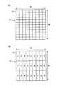
図2(B)は、実施形態1に係る積層型撮像素子の輝度用素子10のピクセル11の平面構成の一例を示した図であり、図2(C)は、実施形態1に係る積層型撮像素子の色用素子70のサブピクセル71の平面構成の一例を示した図である。 FIG. 2B is a diagram illustrating an example of a planar configuration of the
図2(B)に示すように、輝度用素子10は、3N×3M画素(N、Mは自然数)のピクセル(画素)11で構成される。一方、図2(C)に示すように、色用素子70は、3N×M画素のサブピクセル(副画素)71で構成され、1つのサブピクセル71の面積は、輝度用素子のピクセル11の3倍の大きさとなっている。 As shown in FIG. 2B, the luminance element 10 is composed of pixels (pixels) 11 of 3N × 3M pixels (N and M are natural numbers). On the other hand, as shown in FIG. 2C, the color element 70 is composed of 3N × M pixel sub-pixels (sub-pixels) 71, and the area of one
色用素子70の各サブピクセル71の前面には、同色のR、G又はBのカラーフィルタをストライプ状に形成している。よって、各色のサブピクセル71の数は、N×M画素となる。かかる構成とすると、色用素子70の各色の解像度は、輝度用素子10の解像度と比較して、(1/3)×(1/3)=1/9と低くなるが、人間の眼の視覚特性により、色は輝度の(1/4)×(1/4)=1/16程度であっても、実用上問題無いことが知られている。よって、色用素子70の解像度は、輝度用素子10とのバランスにおいて、実用上問題の無いレベルに設定されている。 R, G, or B color filters of the same color are formed in stripes on the front surface of each
輝度用素子10は、入射光のうち、可視光成分領域(波長380nm付近〜780nm付近の波長範囲)において、一様に40〜70%の範囲の強度の光を吸収して輝度信号を出力するとともに、残りの可視光を一様に透過させる。輝度用素子10を透過した光は色用素子70に入射し、カラーフィルタでR、G、Bの各色成分に分光された後、それぞれのサブピクセル71の色信号として出力される。 The luminance element 10 uniformly absorbs light having an intensity in the range of 40 to 70% in the visible light component region (wavelength range near wavelength 380 nm to 780 nm) of incident light and outputs a luminance signal. At the same time, the remaining visible light is uniformly transmitted. The light transmitted through the luminance element 10 enters the color element 70, is split into R, G, and B color components by the color filter, and is then output as a color signal of each
なお、輝度用素子10の透過率は、30〜60%であることが好ましいが、30〜55%であることがより好ましく、40〜50%程度であることが更に好ましく、50%程度であることが特に好ましい。基本的に、輝度用素子10と色用素子70の光の利用率は、両者で1:1となることが好ましいので、輝度用素子10の光透過率は50%程度であることが好ましいが、色用素子70で色成分が十分に取得できる場合には、輝度成分の利用率(=100−透過率)を50%よりも若干高くするようにしてもよい。輝度用素子10の透過率は、このような観点から、用途、色用素子70とのバランス等を考慮して、適宜好ましい透過率に設定することができる。 Note that the transmittance of the luminance element 10 is preferably 30 to 60%, more preferably 30 to 55%, still more preferably about 40 to 50%, and about 50%. It is particularly preferred. Basically, the light utilization factor of the luminance element 10 and the color element 70 is preferably 1: 1 for both, so that the light transmittance of the luminance element 10 is preferably about 50%. When the color component 70 can sufficiently acquire the color component, the luminance component utilization factor (= 100−transmittance) may be slightly higher than 50%. From such a viewpoint, the transmittance of the luminance element 10 can be appropriately set to a preferable transmittance in consideration of the use, balance with the color element 70, and the like.
本実施形態に係る積層型撮像素子と、従来のRGBストライプ方式での撮像素子とについて、図2(A)に示した3N×3M画素のうち、1画素に入射する光量を1として、光の利用率を比較する。従来のRGBストライプ方式で3N×3M画素のカラー撮像画像を得るためには、3N×3M×3サブピクセルが必要となる。その際、1画素に入射する光量のうち、各色のサブピクセルで利用できる光は、既に説明した通り、面積で1/3、各色の波長で1/3となり、全体では1/3×1/3=1/9となる。 For the stacked image sensor according to the present embodiment and the image sensor of the conventional RGB stripe method, the amount of light incident on one pixel of the 3N × 3M pixels shown in FIG. Compare usage rates. In order to obtain a color captured image of 3N × 3M pixels by the conventional RGB stripe method, 3N × 3M × 3 subpixels are required. At that time, out of the amount of light incident on one pixel, the light that can be used in the subpixels of each color is 1/3 in area and 1/3 in the wavelength of each color, as described above. 3 = 1/9.
一方、本実施形態に係る積層型撮像素子では、3N×3M画素のカラー撮像画像を得るために必要なサブピクセル数は、3N×3M(輝度用素子)+3N×M(色用素子)=3N×4Mである。輝度用素子10では、総ての可視波長領域の光を40〜70%吸収するため、利用できる光は、60〜30%となる。ここで、例えば、輝度用素子10の光吸収率を50%とすると、色用素子70で利用できる光量は1/2となる。一方、色用素子70については、入射する光量自体が1/2、各色の波長で1/3となるが、面積が輝度用素子10の3倍であるため、結局、色用素子70でも1/2の光量を利用することができる。よって、従来のRGBストライプ方式と比較しても、特許文献1に記載した方式の輝度用素子で1/2、色用素子で1/6の光利用率と比較しても、感度や色再現性の向上が期待できる。 On the other hand, in the stacked image sensor according to the present embodiment, the number of subpixels necessary to obtain a color captured image of 3N × 3M pixels is 3N × 3M (luminance element) + 3N × M (color element) = 3N. × 4M. Since the luminance element 10 absorbs 40 to 70% of light in the entire visible wavelength region, the available light is 60 to 30%. Here, for example, if the light absorptance of the luminance element 10 is 50%, the amount of light that can be used by the color element 70 is ½. On the other hand, with respect to the color element 70, the incident light quantity itself is ½, and the wavelength of each color is 、. However, since the area is three times that of the luminance element 10, the color element 70 is eventually 1 A light quantity of / 2 can be used. Therefore, even if compared with the conventional RGB stripe method, and compared with the light utilization factor of 1/2 in the luminance element of the method described in Patent Document 1 and 1/6 in the color element, the sensitivity and color reproduction. The improvement of sex can be expected.
図3は、本実施形態に係る積層型撮像素子の入力像の焦点について説明するための図である。図3において、撮影レンズ100と、撮影レンズ100による焦点Pと、撮影レンズ100の焦点深度Dが示されている。焦点深度Dは、撮像画像のピントが合って見える許容範囲を意味する。撮影レンズ100は、本実施形態に係る積層型撮像素子の前方、つまり入射光側に配置される。 FIG. 3 is a diagram for explaining the focus of the input image of the multilayer image sensor according to the present embodiment. In FIG. 3, the photographing
図3に示す入力像の焦点Pは、入射光側に配置された輝度用素子10に焦点を合わせることが好ましい。つまり、入力像の焦点Pが、色用素子70ではなく、輝度用素子10の位置に合うように撮影レンズ100を設定することが好ましい。具体的には、例えば、輝度用素子10が光電変換膜等の受光素子を備える場合には、かかる受光素子の厚さ方向の中心付近が、焦点深度Dの範囲内に位置するように設定すればよい。 The focus P of the input image shown in FIG. 3 is preferably focused on the luminance element 10 arranged on the incident light side. That is, it is preferable to set the
焦点Pを色用素子70ではなく輝度用素子10側に合わせるのは、色用素子70については、多少、受光面がレンズの結像面から光軸方向にずれている状態であり、デフォーカスしている方が偽色の発生を抑制することができるからである。色用素子70上でデフォーカスしている場合、他色の周辺画素領域の色成分も混入するため、画素近傍の平均の色成分を撮像するという目的に合致する。つまり、色用素子70に焦点Pが合っていると、カラーフィルタで各色の波長成分にほぼ完全に分光され、他の色はほぼ完全に遮蔽されてしまうが、デフォーカスして若干ボケていれば、周辺の他色のカラーフィルタからクロスするように入射する色成分を各色用ピクセル71で受光することができ、より広い領域を平均化させた色成分を有する状態で透過光を受光することができるからである。また、上述のように、色成分は、輝度成分の(1/4)×(1/4)=1/16程度の解像度でも視覚上の問題が無いため、デフォーカスの程度も輝度成分の画素11の4×4=16倍程度までの範囲で、任意に設定することができる。 The focus P is adjusted not to the color element 70 but to the luminance element 10 side because the light receiving surface of the color element 70 is slightly shifted from the lens imaging surface in the optical axis direction. This is because the generation of false colors can be suppressed. When defocusing is performed on the color element 70, the color components of the peripheral pixel regions of other colors are also mixed in, so that the purpose of imaging the average color component in the vicinity of the pixels is met. In other words, when the color element 70 is in focus P, the color filter almost completely separates the wavelength components of each color and the other colors are almost completely shielded, but they are defocused and slightly blurred. For example, each
撮影レンズ100の焦点深度Dは、レンズの絞り値F、許容錯乱円(画素ピッチ)δと(1)式の関係にある。なお、レンズの絞り値Fは、レンズの大きさに対する絞りの大きさを示す調整値であり、許容錯乱円は、撮像画像のピントが合っているように見える領域の広さを示す値である。 The depth of focus D of the

次に、本実施例に係る積層型撮像素子の信号処理について詳細に説明する。色用素子70のR、G、Bそれぞれの振動出力を内挿して、輝度用素子10の画素11の位置と対応させたものをRc(i,j)、Gc(i,j)、Bc(i,j)とする。ここで、(i,j)は画素位置を表す。画素(i,j)に対応する輝度用素子10の出力をL(i,j)、求めたい各画素位置のRGBの値をR(i,j)、G(i,j)、B(i,j)とする。輝度用素子10の波長に対する感度が理想的に一様な場合、(2)式が成立する。 Next, signal processing of the multilayer image sensor according to the present embodiment will be described in detail. Rc (i, j), Gc (i, j), Bc (Rc (i, j), Bc () corresponding to the position of the
但し、輝度用素子10のピクセル11と色用素子70のピクセル71とが、境界線が一致して重なっていない配置の場合には、(1)〜(9)式を用いて説明した演算はより複雑なものとなる。よって、図2(B)、(C)に示したように、輝度用素子10のピクセル11の3画素分と色用素子70のサブピクセル71の1画素分が1対1に対応し、上下に重なるような配置とすることが、演算処理上好ましい。 However, when the
〔実施形態2〕
図4は、本発明の実施形態2に係る積層型撮像素子の一例の平面構成を示した図である。図4(A)は、実施形態2に係る積層型撮像素子の輝度用素子12のピクセル13の平面構成を示した図であり、図4(B)は、実施形態2に係る積層型撮像素子の色用素子72のサブピクセル73の平面構成を示した図である。[Embodiment 2]
FIG. 4 is a diagram illustrating a planar configuration of an example of a multilayer imaging element according to Embodiment 2 of the present invention. 4A is a diagram illustrating a planar configuration of the
実施形態2に係る積層型撮像素子の側面構成は、図2(A)で示した構成と同様であり、入射光側に輝度用素子12が配置され、輝度用素子12の背面に色用素子72が配置された構成となっているので、図示を省略している。また、かかる輝度用素子12を入射光側、色用素子72を輝度用素子12の背面に配置した構成の利点は、実施形態1における説明と同様であるので、その説明を省略する。 The side surface configuration of the multilayer imaging element according to the second embodiment is the same as the configuration shown in FIG. 2A, the
図4(A)において、輝度用素子12の平面構成が示されており、ピクセル13が3N×2M画素配列されている。各ピクセル13は、入射光を受光し、輝度成分を取得することができれば、図2(A)に示したピクセル11と同様の構成であってもよいし、異なる構成であってもよい。実施形態2に係る積層型撮像素子の輝度用素子12は、配列されたピクセル数が、3N×2M(N、Mは自然数)で表示されている点だけが実施形態1と異なっており、ピクセル13の配列についても、本質的な相違点は無い。特に、Mが3の倍数である場合には、実施形態1と画素数の表示の仕方が異なっているだけであり、全く同一の画素配列であってもよい。 FIG. 4A shows a planar configuration of the
一方、図4(B)において、色用素子72は、R、G、Bがストライプ状に配置された点は実施形態1の色用素子70と同様であるが、各サブピクセル73の面積が、輝度用素子12のピクセル13の2倍の大きさである点で、3倍の大きさである実施形態1の色用素子70と異なっている。これにより、色用素子72のサブピクセル73の数は、3N×Mとなり、輝度用素子10のピクセル13の1/2となっている。 On the other hand, in FIG. 4B, the
このように、色用素子72のサブピクセル73の面積は、輝度用素子12のピクセル13の2倍に設定されていてもよい。なお、実施形態2に係る色用素子72のサブピクセル73は、輝度用素子12の縦方向に隣接する2画素分のピクセル13を合わせた大きさとなっている。色用素子72のサブピクセル73を、輝度用素子12の縦方向に隣接する2つのピクセル13に対応させた縦長の長方形のピクセルとし、同じ色用のサブピクセル73を同一列に配置することにより、実施形態1に係る積層型撮像素子の色用素子70と同様に、全体としてはRGBストライプ方式と同じ配置とすることができる。 Thus, the area of the sub-pixel 73 of the
なお、輝度用素子12は、実施形態1に係る積層型撮像素子の輝度用素子10と同様に、透過率な30〜60%の範囲で用途に応じて任意に設定することができるが、例えば、透過率を50%に設定した場合について考える。 The
輝度用素子12の光透過率を50%とした場合、入射光の1/2の光量が輝度用素子12を透過し、輝度用素子12で利用できる光量は入射光の光量の1/2となる。色用素子72においては、輝度用素子12を透過した入射光の1/2の光量を受光する。また、各色の波長で利用できる光量は受光した光の1/3となるが、各サブピクセル73の面積は、輝度用素子12の2倍であるため、色用素子72の各色のサブピクセル73で利用できる光量は、輝度用素子12の入射光の光量の(1/2)×(1/3)×2=1/3となる。このように、実施形態2に係る積層型撮像素子においては、輝度用素子12で利用できる光量と色用素子72の各色のサブピクセル73で利用できる光量を適切にバランスさせ、高感度と色再現性を両立させることができる。 When the light transmittance of the
ここで、従来の方式では、3N×2M画素のカラー撮像画像を得るためには、3N×2M×3のサブピクセルが必要となる。一方、本実施形態に係る積層型撮像素子の場合、3N×2M画素のカラー撮像画像を得るために必要なサブピクセル数は、3N×2M(輝度用素子)+3N×M(色用素子)=3N×3Mとなる。 Here, in the conventional method, 3N × 2M × 3 sub-pixels are required to obtain a color captured image of 3N × 2M pixels. On the other hand, in the case of the multilayer imaging device according to the present embodiment, the number of subpixels required to obtain a color captured image of 3N × 2M pixels is 3N × 2M (luminance element) + 3N × M (color element) = 3N × 3M.
なお、図4において、輝度用素子12のピクセル13が縦に隣接した2個分と、色用素子72のサブピクセル73の1個が1対1に対応して重なり、外側の境界線が一致した配置となっている例を挙げて説明したが、これらの1対1の対応は必須ではなく、色用素子72のサブピクセル73が輝度用素子12のピクセル13の2倍の面積を有していれば、色用素子72の光の利用度を高めることができる。 In FIG. 4, two
〔実施形態3〕
図5は、本発明の実施形態3に係る積層型撮像素子の一例の平面構成を示した図である。図5(A)は、実施形態3に係る積層型撮像素子の輝度用素子14のピクセル15の平面構成の一例を示した図であり、図5(B)は、実施形態3に係る積層型撮像素子の色用素子のサブピクセル75の平面構成の一例を示した図である。[Embodiment 3]
FIG. 5 is a diagram illustrating a planar configuration of an example of a multilayer imaging element according to Embodiment 3 of the present invention. FIG. 5A is a diagram illustrating an example of a planar configuration of the
実施形態3に係る積層型撮像素子においても、側面構成は、図2(A)に示した構成と同様である。つまり、光の入射面側に輝度用素子14が配置されて入射光を受光し、輝度用素子14の背面に色用素子74が配置され、輝度用素子14の透過光を受光する。これにより、輝度用素子14で最初に一様に輝度成分を取得し、その後、色用素子74で各色の波長成分のバランスが崩れていない透過光から色成分を取得できる点は、実施形態1における説明と同様であるので、本実施形態においてはその説明を省略する。 Also in the multilayer imaging element according to Embodiment 3, the side surface configuration is the same as the configuration shown in FIG. That is, the
図5(A)に示すように、実施形態3に係る積層型撮像素子の輝度用素子14は、3N×4M(N、Mは自然数)個のピクセル15を備えている。個々のピクセル15は、入射光の輝度成分を取得できれば、実施形態1又は実施形態2に係る構成と同様であってもよいし、異なっていてもよい。また、輝度用素子15は、入射光の40〜70%の光量を吸収し、光透過率は30〜60%となる点も、実施形態1及び実施形態2に係る積層型撮像素子と同様である。 As shown in FIG. 5A, the
図5(B)に示すように、実施形態3に係る積層型撮像素子の色用素子74は、3N×M個のサブピクセル75を備えており、各サブピクセル75は、輝度用素子14のピクセル15の面積の4倍の面積を有している。また、色用素子74のサブピクセル75は、縦方向に隣接する輝度用素子14のピクセル15の4個分をまとめたものに相当し、縦:横=4:1の縦長の長方形となっている。そして、各列は、同じ色用のサブピクセル75が配置され、全体としては、RGBストライプ方式と同様の配置方式となっている。 As shown in FIG. 5B, the
このように、色用素子74のサブピクセル75を、輝度用素子14のピクセル15を縦方向に4個まとめて、4倍の面積として構成してもよい。色用素子74の1つのサブピクセル75で利用する光量を、輝度用素子14と同じ面積のピクセルを用いた場合の4倍とすることができ、光の利用率を高めることができる。 In this way, the
例えば、輝度用素子14の光透過率を50%とすると、光吸収率も50%であるので、輝度用素子14で利用できる入射光の光量は1/2となる。よって、色用素子74は、輝度用素子14を透過した透過光を受光するので、入射する光量は輝度用素子14に入射する入射光の光量の1/2となる。また、各色のフィルタでは、他の2色の波長を遮蔽するので、各色のサブピクセル75は、受光した光量の1/3を利用するが、サブピクセル75の面積が4倍となっているので、結局、各サブピクセル75は、輝度用素子に入射する入射光の(1/2)×(1/3)×4=2/3を利用することができる。 For example, if the light transmittance of the
なお、図5(A)に示すように、本実施形態に係る積層型撮像素子の画素数を3N×4Mとしたときに、従来の方式で3N×4M画素のカラー撮像画像を得るためには、3N×4M×3個のサブピクセルが必要となる。本実施形態に係る積層型撮像素子では、3N×4M画素のカラー撮像画像を得るために必要なサブピクセル数は、3N×4M(輝度用素子14)+3N×M(色用素子74)=3N×5Mとなる。 As shown in FIG. 5A, when the number of pixels of the multilayer imaging device according to the present embodiment is 3N × 4M, in order to obtain a color captured image of 3N × 4M pixels by the conventional method. 3N × 4M × 3 sub-pixels are required. In the multilayer imaging device according to the present embodiment, the number of subpixels required to obtain a color captured image of 3N × 4M pixels is 3N × 4M (luminance element 14) + 3N × M (color element 74) = 3N. × 5M.
また、図5(A)においては、輝度用素子14の縦に隣接するピクセル15の4個分と、色用素子74のサブピクセル75が重なって1対1に対応し、サブピクセル75間の境界線がピクセル15間の対応箇所の境界線に一致している例を挙げて説明したが、このような構成が必須でない点は、実施形態1及び実施形態2と同様である。 In FIG. 5A, four
また、実施形態1乃至3においては、色用素子70、72、74のサブピクセル71、73、75の各色の配列を、同一色が同一列に配置されるRGBストライプ方式となる配置を例に挙げて説明したが、他の配列方法で配置してもよい。例えば、2行2列の4個のサブピクセル71、73、75を1画素とし、2個のGを一方の対角線上、他方の対角線上にRとBを1個ずつ配置したベイヤー配列としてもよい。その他、インターライン配列、斜めストライプ配列、GストライプRB市松配列等の原色配列や、フィールド色差順次配列、フレーム色差順次配列、フレーム色差順次配列、フレームインターリーブ配列、フィールドインターリーブ配列の補色配列方式等、単板用のカラーフィルタ配列で用いられる各種の配列方式を適用することができる。 In the first to third embodiments, the arrangement of the colors of the sub-pixels 71, 73, and 75 of the
〔実施形態4〕
図6は、本発明の実施形態4に係る積層型撮像素子の一例の断面構成を示した図である。実施形態1乃至3においては、輝度用素子10、12、14及び色用素子70、72、74の平面的な画素構成を中心に説明したが、実施形態4以降においては、輝度用素子10、12、14及び色用素子70、72、74の、信号処理を行うための構成も含めた全体構成について説明する。よって、実施形態4以降に説明する積層型撮像素子には、実施形態1乃至3に係る輝度用素子10、12、14及び色用素子70、72、74の画素構成を総て適用することができる。[Embodiment 4]
FIG. 6 is a diagram illustrating a cross-sectional configuration of an example of a multilayer imaging element according to Embodiment 4 of the present invention. In the first to third embodiments, the description has focused on the planar pixel configuration of the
図6において、実施形態4に係る積層型撮像素子は、輝度用素子16と、色用素子76とを有し、色用素子76上に輝度用素子16が配置される。輝度用素子16は、光の入射側から、透明電極20と、光電変換膜30と、画素電極40と、信号読み出し回路50と、透明基板60とを有する。 In FIG. 6, the multilayer imaging device according to the fourth embodiment includes a luminance element 16 and a color element 76, and the luminance element 16 is disposed on the color element 76. The luminance element 16 includes a transparent electrode 20, a photoelectric conversion film 30, a pixel electrode 40, a signal readout circuit 50, and a transparent substrate 60 from the light incident side.
透明電極20は、光電変換膜30に電圧を印加するための電極であり、可視光が透過する透明性の高い材料から構成される。一例としては、インジウム錫酸化膜(ITO、Indium Tin Oxide)等の無機透明電極、又はPolyethylene dioxythiophene polystyrene sulphonate(PED/PSS)等の有機導電膜が用いられてよい。透明電極20に印加する電圧は、光電変換膜30にかかる電界として、103〜107V/cmの範囲がよく、一般的には104〜106V/cmの範囲で用いることが好ましい。The transparent electrode 20 is an electrode for applying a voltage to the photoelectric conversion film 30 and is made of a highly transparent material that transmits visible light. As an example, an inorganic transparent electrode such as indium tin oxide (ITO) or an organic conductive film such as polyethylene dioxythiophene polystyrene sulphonate (PED / PSS) may be used. The voltage applied to the transparent electrode 20 is preferably in the range of 103 to 107 V / cm as the electric field applied to the photoelectric conversion film 30, and is generally preferably used in the range of 104 to 106 V / cm. .
光電変換膜30の材料は、可視光の光(380〜780nm)を、50%程度の吸収率で吸収し、吸収した光量に応じた電荷を発生する一方、吸収しなかった光は透過する材料であり、一例を挙げると、有機系の材料を用いた膜が好ましい。具体的には、ポリフィリン、ペリレン、フタロシアニン、アクリジン、クマリン、キナクリドン、シアニン、スクエアリリウム、オキサジン、キサンテントリフェニルアミン、ベンジジン、ピラゾリン、スチリルアミン、ヒドラゾン、トリフェニルメタン、カルバゾール、ポリシラン、チオフェン、ポリアミン、オキサジアゾール、トリアゾール、トリアジン、キノキサリン、フェナンスロリン、フラーレン、アルミニウムキノリン、ポリパラフェニレンビニレン、ポリフルオレン、ポリビニルカルバゾール、ポリチオール、ポリピロール、ポリチオフェン及びこれらの誘導体等を単独で、若しくは、これらに代表される有機材料を2種類以上混合又は積層することで、光電変換膜30を形成することが可能である。 The material of the photoelectric conversion film 30 is a material that absorbs visible light (380 to 780 nm) with an absorptance of about 50% and generates charges according to the amount of light absorbed, while transmitting light that has not been absorbed. For example, a film using an organic material is preferable. Specifically, polyphylline, perylene, phthalocyanine, acridine, coumarin, quinacridone, cyanine, squarylium, oxazine, xanthenetriphenylamine, benzidine, pyrazoline, styrylamine, hydrazone, triphenylmethane, carbazole, polysilane, thiophene, polyamine, Oxadiazole, triazole, triazine, quinoxaline, phenanthroline, fullerene, aluminum quinoline, polyparaphenylene vinylene, polyfluorene, polyvinyl carbazole, polythiol, polypyrrole, polythiophene, and derivatives thereof are singly or typified by these The photoelectric conversion film 30 can be formed by mixing or laminating two or more organic materials.
一方、アモルファスセレン、アモルファスシリコン、化合物半導体等に代表される無機光電変換膜を用いることもできる。 On the other hand, an inorganic photoelectric conversion film typified by amorphous selenium, amorphous silicon, a compound semiconductor, or the like can also be used.
これら光電変換膜30の膜厚は、10nm〜5μmが好ましく、50nm〜1μmが更に好ましいが、上述の通り、光電変換膜30の透過率を30〜60%、例えば、50%程度に制御する必要がある。 The film thickness of these photoelectric conversion films 30 is preferably 10 nm to 5 μm, more preferably 50 nm to 1 μm, but as described above, the transmittance of the photoelectric conversion film 30 needs to be controlled to 30 to 60%, for example, about 50%. There is.
光電変換膜30の下面には、画素電極40が設けられる。画素電極40も、可視光が透過する透明性の高い材料で構成される。一例としては、インジウム錫酸化膜(ITO)等の無機透明電極、又はPolyethylene dioxythiophene polystyrene sulphonate(PED/PSS)等の有機導電膜が好ましい。 A pixel electrode 40 is provided on the lower surface of the photoelectric conversion film 30. The pixel electrode 40 is also made of a highly transparent material that transmits visible light. As an example, an inorganic transparent electrode such as indium tin oxide film (ITO) or an organic conductive film such as polyethylene dioxythiophene polystyrene sulphonate (PED / PSS) is preferable.
信号読み出し回路50は、各画素に蓄積された信号を読み出す手段である。信号読み出し回路50の一例としては、薄膜トランジスタ(TFT、Thin Film Transistor)を用いた回路が挙げられる。薄膜トランジスタは、ガラス基板上に形成される一般的なものであってよい。電極及び配線には金属材料、半導体層にはアモルファスシリコンや多結晶シリコン等が用いられるが、薄膜トランジスタの開口率(透過率)を高めたい場合には、電極及び配線材料としてITO等の透明電極材料、半導体層としてZnOやInGaZnO4等、結晶系又は非晶質系の透明半導体材料を用いてよい。The signal readout circuit 50 is means for reading out signals accumulated in each pixel. An example of the signal readout circuit 50 is a circuit using a thin film transistor (TFT). The thin film transistor may be a general one formed on a glass substrate. Metal materials are used for the electrodes and wiring, and amorphous silicon, polycrystalline silicon, etc. are used for the semiconductor layer. However, in order to increase the aperture ratio (transmittance) of the thin film transistor, a transparent electrode material such as ITO is used as the electrode and wiring material. As the semiconductor layer, a crystalline or amorphous transparent semiconductor material such as ZnO or InGaZnO4 may be used.
なお、実施形態1乃至3において説明した輝度用素子16のピクセル11、13、15の単位は、信号読み出し回路50の単位で定められる。つまり、1画素に対して、信号読み出し用の薄膜トランジスタ等の素子が1個設けられることになる。 Note that the unit of the
透明基板60は、一般的にはガラス基板が用いられるが、透明基板60上の信号読み出し回路50、光電変換膜30、透明電極20等が150℃乃至200℃以下の温度条件で作製できる場合には、種々のプラスチック基板を用いることも可能である。 A glass substrate is generally used as the transparent substrate 60, but the signal readout circuit 50, the photoelectric conversion film 30, the transparent electrode 20, and the like on the transparent substrate 60 can be manufactured under a temperature condition of 150 ° C. to 200 ° C. or less. It is also possible to use various plastic substrates.
色用素子76は、カラーフィルタ80と、色用素子用撮像素子90とを有して構成される。色用素子用撮像素子90には、通常の撮像素子として一般的に用いられている電荷結合素子(Charge Coupled Device:CCD)や、相補型金属−酸化物半導体(Complementary Metal-Oxide Semiconductor:CMOS)等を用いた固体撮像素子が好適である。また、アモルファスシリコン、アモルファスセレン、化合物半導体材料等の無機材料、可視領域全域に亘って感度を有する有機材料等を光電変換膜として用い、これらの膜を積層し、信号読み出し部としてCCD、CMOS、TFT回路等を用いるようにしてもよい。 The color element 76 includes a color filter 80 and a color
また、色用素子76における実施形態1乃至3で説明したピクセル71、73、75の単位は、輝度用素子16と同様に、固体撮像素子のCCD、CMOS等の素子の単位、光電変換膜の信号読み出し部のCCD、CMOS、TFT回路等の素子の単位により定められる。つまり、1ピクセル71、73、75に対し、1個の素子が設けられる。 The units of the
かかる構成により、輝度用素子16の光電変換膜30で受光した光信号を信号読み出し回路50で読み出し、色用素子76で受光した透過光を色用素子用撮像素子90に設けられた信号読み出し部で読み出すことにより、高感度で色再現性の高い撮像を行うことができる。 With this configuration, the optical signal received by the photoelectric conversion film 30 of the luminance element 16 is read by the signal readout circuit 50, and the transmitted light received by the color element 76 is provided in the color
なお、図6においては、透明基板60とカラーフィルタ80の間に隙間を設けた配置としているが、用途と焦点調整に応じて、透明基板60とカラーフィルタ80を密着させた配置としてもよい。 In FIG. 6, the gap is provided between the transparent substrate 60 and the color filter 80, but the transparent substrate 60 and the color filter 80 may be arranged in close contact according to the application and focus adjustment.
〔実施形態5〕
図7は、本発明の実施形態5に係る積層型撮像素子の一例の断面構成を示した図である。実施形態5に係る積層型撮像素子は、色用素子77の上に輝度用素子17が配置されている点は、実施形態4に係る積層型撮像素子と同様であるが、色用素子77のカラーフィルタ80の上に層間絶縁膜61が付設されており、層間絶縁膜61上に輝度用素子17が設けられている点で、実施形態4に係る積層型撮像素子と異なっている。そして、層間絶縁膜61上に、信号読み出し回路50、画素電極40、光電変換膜30及び透明電極20が順次形成され、輝度用素子17を構成している。[Embodiment 5]
FIG. 7 is a diagram showing a cross-sectional configuration of an example of a multilayer imaging element according to Embodiment 5 of the present invention. The multilayer image sensor according to the fifth embodiment is the same as the multilayer image sensor according to the fourth embodiment in that the luminance element 17 is disposed on the color element 77. An interlayer insulating
輝度用素子17の透明電極20、光電変換膜30、画素電極40及び信号読み出し回路50は、実施形態4に係る積層型撮像素子の輝度用素子16と同様であるので、同一の参照符号を付してその説明を省略する。 The transparent electrode 20, the photoelectric conversion film 30, the pixel electrode 40, and the signal readout circuit 50 of the luminance element 17 are the same as the luminance element 16 of the multilayer imaging element according to the fourth embodiment, and thus are denoted by the same reference numerals. Therefore, the description is omitted.
色用素子77のカラーフィルタ80及び色用素子用撮像素子90も、実施形態4に係る積層型撮像素子の色用素子76と同様であるので、同一の参照符号を付してその説明を省略する。 The color filter 80 of the color element 77 and the color
層間絶縁膜61は、高い透過性が要求され、酸化珪素、窒化珪素、各種樹脂等を用いることができる。 The
このように、実施形態4のように、透明基板60の上に輝度用素子16を独立して形成した後、色用素子76の上に配置するのではなく、実施形態5のように、色用素子77を最初に形成し、その上に層間絶縁膜61を形成し、層間絶縁膜61上に輝度用素子17を一体的に積層形成するようにしてもよい。一体化して構成することにより、積層型撮像素子の全体の体積を小型化することができる。 As described above, the luminance element 16 is independently formed on the transparent substrate 60 as in the fourth embodiment, and is not disposed on the color element 76. It is also possible to first form the device element 77, form the
なお、実施形態5に係る積層型撮像素子は、輝度用素子17の信号読み取りは、信号読み取り回路50で行い、色用素子77の信号読み出しは、色用素子用撮像素子90の信号読み出し部で行い、両者が独立して信号読み出しを行う点は、実施形態4に係る積層型撮像素子と同様である。 In the multilayer image sensor according to the fifth embodiment, the signal reading of the luminance element 17 is performed by the signal reading circuit 50, and the signal reading of the color element 77 is performed by the signal reading unit of the color
〔実施形態6〕
図8は、本発明の実施形態6に係る積層型撮像素子の一例の断面構成を示した図である。
実施形態6に係る積層型撮像素子は、輝度用素子18と色用素子28の信号読み出し回路(図示せず)が同一箇所に配置されている点で、実施形態4及び実施形態5に係る積層型撮像素子と異なっている。[Embodiment 6]
FIG. 8 is a diagram showing a cross-sectional configuration of an example of a multilayer imaging element according to Embodiment 6 of the present invention.
The multilayer imaging device according to the sixth embodiment is a multilayer imaging device according to the fourth and fifth embodiments in that signal readout circuits (not shown) of the luminance element 18 and the color element 28 are arranged at the same place. This is different from the type image sensor.
実施形態6に係る積層型撮像素子は、色用素子28と、色用素子28の上に積層された輝度用素子18とを有する。輝度用素子18は、透明電極20と、光電変換膜30と、画素電極41とを備える。色用素子28は、カラーフィルタ81と、色用素子用撮像素子91とを有し、カラーフィルタ81には、ビアプラグ82が形成されて設けられている。 The multilayer image sensor according to the sixth embodiment includes a color element 28 and a luminance element 18 stacked on the color element 28. The luminance element 18 includes a transparent electrode 20, a photoelectric conversion film 30, and a pixel electrode 41. The color element 28 includes a color filter 81 and a color
色用素子28の色用素子用撮像素子91は、色用素子28の信号読み取り手段のみならず、輝度用素子18の信号読み出し回路も備えており、輝度用素子18の画素電極41とビアプラグ82を介して接続されている。色用素子用撮像素子91は、色用素子28の受光部、信号読み出し部に加えて、輝度用素子18の信号読み出し回路も備える必要があることから、CCDやCMOSイメージセンサを用いることが好ましい。輝度用素子18を構成する透明電極20、光電変換膜30、画素電極41及び輝度用素子18と色用素子28とを隔てる層間絶縁膜材料は、実施形態4で述べた材料と同様の材料を使用することができる。 The color
このように、実施形態6に係る積層型撮像装置によれば、輝度用素子18と色用素子28の信号読み出し回路を共通回路とし、1箇所に設けることにより、積層型撮像素子を薄型化して構成することができる。 As described above, according to the multilayer imaging device according to the sixth embodiment, the signal readout circuit of the luminance element 18 and the color element 28 is a common circuit, and the multilayer imaging element is thinned by providing the signal readout circuit in one place. Can be configured.
〔実施例〕
次に、本実施形態に係る積層型撮像装置について、シミュレーション実験を行った結果の実施例について説明する。〔Example〕
Next, an example of a result of performing a simulation experiment on the multilayer imaging device according to the present embodiment will be described.
条件としては、実施形態4で説明した実施形態と同様に、透明基板60上に輝度用素子16を形成し、輝度用素子16と色用素子76の信号読み出し回路は独立に設けた。輝度用素子16と、色用素子76の撮像面との距離は約0.4mmとし、透明基板60の厚さと同等とした。なお、本実施例においては、理解の容易のため、実施形態4に対応する構成要素については、実施形態4で用いた参照符号と同一の符号を付して説明する。 As a condition, as in the embodiment described in the fourth embodiment, the luminance element 16 is formed on the transparent substrate 60, and the signal readout circuits of the luminance element 16 and the color element 76 are provided independently. The distance between the luminance element 16 and the imaging surface of the color element 76 was about 0.4 mm, which was the same as the thickness of the transparent substrate 60. In the present example, for ease of understanding, the components corresponding to the fourth embodiment will be described with the same reference numerals as those used in the fourth embodiment.
輝度用素子16は、ピクセル数を、水平128×垂直96とし、ピクセルサイズを、100×100μmとした。また、透明電極20には、膜厚30nmのITOを用いた。光電変換膜30は、キナクリドン誘電体にフラーレンを25%添加した膜厚75nmの薄膜を真空蒸着法にて成膜して形成した。波長が530nmの緑色の波長領域では、透過率が56%であった。画素電極40には、膜厚50nmのITO透明電極を用いた。信号読み出し回路50には、アモルファスシリコンTFTを用いた。透明基板60は、厚さ0.4mmの無アルカリガラスを用いた。 The luminance element 16 has a pixel number of horizontal 128 × vertical 96 and a pixel size of 100 × 100 μm. The transparent electrode 20 was made of ITO having a film thickness of 30 nm. The photoelectric conversion film 30 was formed by forming a thin film having a thickness of 75 nm obtained by adding 25% fullerene to a quinacridone dielectric by a vacuum deposition method. In the green wavelength region having a wavelength of 530 nm, the transmittance was 56%. As the pixel electrode 40, an ITO transparent electrode having a film thickness of 50 nm was used. An amorphous silicon TFT was used for the signal readout circuit 50. As the transparent substrate 60, non-alkali glass having a thickness of 0.4 mm was used.
色用素子76は、サブピクセル数を、水平128×垂直32とし、サブピクセルサイズを、100×300μmとした。これは、実施形態1において説明した、色用素子76の画素の面積を、輝度用素子16の3倍の面積とした場合に相当する。よって、画素数は、垂直方向において96の1/3の32となり、面積は、垂直方向において100μmの3倍の300μmとなっている。カラーフィルタ80の配列も、実施形態1と同様に、ストライプ配列とした。また、色用素子用撮像素子90としては、CMOSイメージセンサを用いた。 In the color element 76, the number of sub-pixels was set to horizontal 128 × vertical 32, and the sub-pixel size was set to 100 × 300 μm. This corresponds to the case where the pixel area of the color element 76 described in the first embodiment is three times as large as the luminance element 16. Accordingly, the number of pixels is 32, which is 1/3 of 96 in the vertical direction, and the area is 300 μm, which is three
また、比較例として、従来から一般的に用いられている、本実施例の輝度用素子16と同画素数、同画素サイズのイメージセンサを用いた。よって、画素数は、水平128×垂直96であり、画素サイズは、100×100μmである。また、カラーフィルタの配列は、ストライプ配列とし、同一条件とした。 Further, as a comparative example, an image sensor having the same number of pixels and the same pixel size as the luminance element 16 of the present embodiment, which has been generally used conventionally, was used. Therefore, the number of pixels is 128 horizontal × 96 vertical, and the pixel size is 100 × 100 μm. The color filters were arranged in a stripe arrangement under the same conditions.
本実施例に係る積層型撮像素子及び比較例に係る撮像素子について、10ルクス(lx)の白色光(色温度3300K)を撮像面に照射したときの出力信号電流の総和を求めたところ、本実施例に係る積層型撮像素子は35nA/lx、比較例に係る撮像素子は23nA/lxとなった。かかる結果から、本実施例に係る積層型撮像素子は、同一の入射光から高い信号電流を出力することができ、入射光の利用率が比較例よりも向上したことを示す結果が得られた。 Regarding the image pickup device according to the present embodiment and the image pickup device according to the comparative example, the total sum of output signal currents when the image pickup surface is irradiated with 10 lux (lx) white light (color temperature 3300 K) is calculated. The multilayer image sensor according to the example was 35 nA / lx, and the image sensor according to the comparative example was 23 nA / lx. From these results, the multilayer imaging device according to the present example was able to output a high signal current from the same incident light, and a result indicating that the utilization rate of the incident light was improved as compared with the comparative example was obtained. .
以上、本発明の好ましい実施形態について詳説したが、本発明は、上述した実施形態に制限されることはなく、本発明の範囲を逸脱することなく、上述した実施形態に種々の変形及び置換を加えることができる。 The preferred embodiments of the present invention have been described in detail above, but the present invention is not limited to the above-described embodiments, and various modifications and substitutions can be made to the above-described embodiments without departing from the scope of the present invention. Can be added.
本発明は、デジタルカメラ、ビデオ等の静止画や動画を撮像する撮像装置全般に利用することができる。 The present invention can be used for all imaging devices that capture still images and moving images such as digital cameras and videos.
10、12、14、16、17、18 輝度用素子
11、13、15 ピクセル(画素)
20 透明電極
30 光電変換膜
40、41 画素電極
50 信号読み出し回路
60 透明基板
70、72、72、76、77、78 色用素子
71、73、75 サブピクセル(副画素)
80 カラーフィルタ
90 色用素子用撮像素子
100 撮影レンズ10, 12, 14, 16, 17, 18
20 Transparent electrode 30 Photoelectric conversion film 40, 41 Pixel electrode 50 Signal readout circuit 60
80
Claims (8)
Translated fromJapanese該第1の撮像素子の背面側に配置され、該第1の撮像素子を透過した透過光を受光し、前記光学像の色成分を取得する第2の撮像素子とを有し、
前記第2の撮像素子のサブピクセルの面積は、前記第1の撮像素子のピクセルの面積の2倍、3倍又は4倍であることを特徴とする積層型撮像素子。A first image sensor that receives incident light and acquires a luminance component of an optical image;
A second imaging element that is disposed on the back side of the first imaging element, receives transmitted light that has passed through the first imaging element, and acquires a color component of the optical image;
The area of the sub-pixel of the second image sensor is two times, three times, or four times the area of the pixel of the first image sensor.
該撮影レンズの焦点は、前記第1の撮像素子に合わせたことを特徴とする請求項1乃至3のいずれか一項に記載の積層型撮像素子。A photographing lens further closer to the incident side of the input light than the first image sensor;
4. The multilayer image sensor according to claim 1, wherein the photographing lens is focused on the first image sensor. 5.
Priority Applications (1)
| Application Number | Priority Date | Filing Date | Title |
|---|---|---|---|
| JP2010228542AJP2012084649A (en) | 2010-10-08 | 2010-10-08 | Laminated imaging device |
Applications Claiming Priority (1)
| Application Number | Priority Date | Filing Date | Title |
|---|---|---|---|
| JP2010228542AJP2012084649A (en) | 2010-10-08 | 2010-10-08 | Laminated imaging device |
Publications (1)
| Publication Number | Publication Date |
|---|---|
| JP2012084649Atrue JP2012084649A (en) | 2012-04-26 |
Family
ID=46243236
Family Applications (1)
| Application Number | Title | Priority Date | Filing Date |
|---|---|---|---|
| JP2010228542APendingJP2012084649A (en) | 2010-10-08 | 2010-10-08 | Laminated imaging device |
Country Status (1)
| Country | Link |
|---|---|
| JP (1) | JP2012084649A (en) |
Cited By (6)
| Publication number | Priority date | Publication date | Assignee | Title |
|---|---|---|---|---|
| JP2016029794A (en)* | 2014-07-18 | 2016-03-03 | 株式会社半導体エネルギー研究所 | Display system, imaging device, monitoring device, display device, and electronic device |
| JP2017135220A (en)* | 2016-01-26 | 2017-08-03 | 日本放送協会 | Imaging device and imaging apparatus |
| JP2017208602A (en)* | 2016-05-16 | 2017-11-24 | キヤノン株式会社 | Image reading device, image forming apparatus, and image reading method |
| WO2019124136A1 (en)* | 2017-12-20 | 2019-06-27 | ソニーセミコンダクタソリューションズ株式会社 | Photoelectric conversion element and solid-state imaging device |
| JP2020017756A (en)* | 2014-07-25 | 2020-01-30 | 株式会社半導体エネルギー研究所 | Imaging device |
| JP2020021855A (en)* | 2018-08-01 | 2020-02-06 | 日本放送協会 | Imaging element and method of manufacturing the same |
Citations (5)
| Publication number | Priority date | Publication date | Assignee | Title |
|---|---|---|---|---|
| JP2006120773A (en)* | 2004-10-20 | 2006-05-11 | Fuji Photo Film Co Ltd | Single layer color solid-state imaging device with photoelectric conversion film |
| JP2009130239A (en)* | 2007-11-27 | 2009-06-11 | Nippon Hoso Kyokai <Nhk> | Color imaging device |
| JP2010123779A (en)* | 2008-11-20 | 2010-06-03 | Sony Corp | Solid-state imaging apparatus and imaging apparatus |
| WO2010095374A1 (en)* | 2009-02-23 | 2010-08-26 | パナソニック株式会社 | Image sensor and image capture device provided with same |
| JP2011238773A (en)* | 2010-05-11 | 2011-11-24 | Panasonic Corp | Composite type imaging element and imaging apparatus having the same |
- 2010
- 2010-10-08JPJP2010228542Apatent/JP2012084649A/enactivePending
Patent Citations (5)
| Publication number | Priority date | Publication date | Assignee | Title |
|---|---|---|---|---|
| JP2006120773A (en)* | 2004-10-20 | 2006-05-11 | Fuji Photo Film Co Ltd | Single layer color solid-state imaging device with photoelectric conversion film |
| JP2009130239A (en)* | 2007-11-27 | 2009-06-11 | Nippon Hoso Kyokai <Nhk> | Color imaging device |
| JP2010123779A (en)* | 2008-11-20 | 2010-06-03 | Sony Corp | Solid-state imaging apparatus and imaging apparatus |
| WO2010095374A1 (en)* | 2009-02-23 | 2010-08-26 | パナソニック株式会社 | Image sensor and image capture device provided with same |
| JP2011238773A (en)* | 2010-05-11 | 2011-11-24 | Panasonic Corp | Composite type imaging element and imaging apparatus having the same |
Cited By (10)
| Publication number | Priority date | Publication date | Assignee | Title |
|---|---|---|---|---|
| JP2016029794A (en)* | 2014-07-18 | 2016-03-03 | 株式会社半導体エネルギー研究所 | Display system, imaging device, monitoring device, display device, and electronic device |
| JP2020017756A (en)* | 2014-07-25 | 2020-01-30 | 株式会社半導体エネルギー研究所 | Imaging device |
| JP2017135220A (en)* | 2016-01-26 | 2017-08-03 | 日本放送協会 | Imaging device and imaging apparatus |
| JP2017208602A (en)* | 2016-05-16 | 2017-11-24 | キヤノン株式会社 | Image reading device, image forming apparatus, and image reading method |
| US10582092B2 (en) | 2016-05-16 | 2020-03-03 | Canon Kabushiki Kaisha | Image reading apparatus with correction for sub-scanning color shifts, image forming apparatus, image reading method, and computer readable non-transitory storage medium |
| WO2019124136A1 (en)* | 2017-12-20 | 2019-06-27 | ソニーセミコンダクタソリューションズ株式会社 | Photoelectric conversion element and solid-state imaging device |
| US11469262B2 (en) | 2017-12-20 | 2022-10-11 | Sony Semiconductor Solutions Corporation | Photoelectric converter and solid-state imaging device |
| US12046610B2 (en) | 2017-12-20 | 2024-07-23 | Sony Semiconductor Solutions Corporation | Photoelectric converter and solid-state imaging device |
| JP2020021855A (en)* | 2018-08-01 | 2020-02-06 | 日本放送協会 | Imaging element and method of manufacturing the same |
| JP7240833B2 (en) | 2018-08-01 | 2023-03-16 | 日本放送協会 | image sensor |
Similar Documents
| Publication | Publication Date | Title |
|---|---|---|
| US20220181567A1 (en) | Solid-state imaging element, production method thereof, and electronic device | |
| US20220285418A1 (en) | Image sensor and electronic apparatus including the same | |
| US10032810B2 (en) | Image sensor with dual layer photodiode structure | |
| TWI788994B (en) | Solid-state imaging element, manufacturing method thereof, and electronic device | |
| US10453898B2 (en) | Solid state image sensor pixel electrode below a photoelectronic conversion film | |
| CN101814517B (en) | Solid-state imaging device and electronic apparatus | |
| US20150304582A1 (en) | Image pickup device and camera system | |
| JP5860168B2 (en) | Solid-state imaging device | |
| JP6947036B2 (en) | Imaging equipment, electronic equipment | |
| JP5032954B2 (en) | Color imaging device | |
| US20190088693A1 (en) | Solid-state imaging device and electronic apparatus | |
| JP6017322B2 (en) | Solid-state imaging device | |
| WO2017145815A1 (en) | Imaging device | |
| JP6010465B2 (en) | Solid-state imaging device | |
| TW201523849A (en) | Solid-state image sensing device | |
| KR20150067005A (en) | Solid-state imaging device | |
| JP2012084649A (en) | Laminated imaging device | |
| JP2022018538A (en) | Imaging device and imaging method | |
| JP2011066685A (en) | Solid-state image sensing element, method for driving the same, and image sensing device |
Legal Events
| Date | Code | Title | Description |
|---|---|---|---|
| A621 | Written request for application examination | Free format text:JAPANESE INTERMEDIATE CODE: A621 Effective date:20130607 | |
| A977 | Report on retrieval | Free format text:JAPANESE INTERMEDIATE CODE: A971007 Effective date:20140320 | |
| A131 | Notification of reasons for refusal | Free format text:JAPANESE INTERMEDIATE CODE: A131 Effective date:20140401 | |
| A02 | Decision of refusal | Free format text:JAPANESE INTERMEDIATE CODE: A02 Effective date:20140924 |