JP2012078692A - Display device - Google Patents
Display deviceDownload PDFInfo
- Publication number
- JP2012078692A JP2012078692AJP2010225624AJP2010225624AJP2012078692AJP 2012078692 AJP2012078692 AJP 2012078692AJP 2010225624 AJP2010225624 AJP 2010225624AJP 2010225624 AJP2010225624 AJP 2010225624AJP 2012078692 AJP2012078692 AJP 2012078692A
- Authority
- JP
- Japan
- Prior art keywords
- substrate
- display device
- color filter
- tft
- liquid crystal
- Prior art date
- Legal status (The legal status is an assumption and is not a legal conclusion. Google has not performed a legal analysis and makes no representation as to the accuracy of the status listed.)
- Pending
Links
Images


Classifications
- G—PHYSICS
- G02—OPTICS
- G02F—OPTICAL DEVICES OR ARRANGEMENTS FOR THE CONTROL OF LIGHT BY MODIFICATION OF THE OPTICAL PROPERTIES OF THE MEDIA OF THE ELEMENTS INVOLVED THEREIN; NON-LINEAR OPTICS; FREQUENCY-CHANGING OF LIGHT; OPTICAL LOGIC ELEMENTS; OPTICAL ANALOGUE/DIGITAL CONVERTERS
- G02F1/00—Devices or arrangements for the control of the intensity, colour, phase, polarisation or direction of light arriving from an independent light source, e.g. switching, gating or modulating; Non-linear optics
- G02F1/01—Devices or arrangements for the control of the intensity, colour, phase, polarisation or direction of light arriving from an independent light source, e.g. switching, gating or modulating; Non-linear optics for the control of the intensity, phase, polarisation or colour
- G02F1/13—Devices or arrangements for the control of the intensity, colour, phase, polarisation or direction of light arriving from an independent light source, e.g. switching, gating or modulating; Non-linear optics for the control of the intensity, phase, polarisation or colour based on liquid crystals, e.g. single liquid crystal display cells
- G02F1/133—Constructional arrangements; Operation of liquid crystal cells; Circuit arrangements
- G02F1/1333—Constructional arrangements; Manufacturing methods
- G02F1/133302—Rigid substrates, e.g. inorganic substrates
- G—PHYSICS
- G02—OPTICS
- G02F—OPTICAL DEVICES OR ARRANGEMENTS FOR THE CONTROL OF LIGHT BY MODIFICATION OF THE OPTICAL PROPERTIES OF THE MEDIA OF THE ELEMENTS INVOLVED THEREIN; NON-LINEAR OPTICS; FREQUENCY-CHANGING OF LIGHT; OPTICAL LOGIC ELEMENTS; OPTICAL ANALOGUE/DIGITAL CONVERTERS
- G02F2201/00—Constructional arrangements not provided for in groups G02F1/00 - G02F7/00
- G02F2201/02—Constructional arrangements not provided for in groups G02F1/00 - G02F7/00 fibre
- G—PHYSICS
- G02—OPTICS
- G02F—OPTICAL DEVICES OR ARRANGEMENTS FOR THE CONTROL OF LIGHT BY MODIFICATION OF THE OPTICAL PROPERTIES OF THE MEDIA OF THE ELEMENTS INVOLVED THEREIN; NON-LINEAR OPTICS; FREQUENCY-CHANGING OF LIGHT; OPTICAL LOGIC ELEMENTS; OPTICAL ANALOGUE/DIGITAL CONVERTERS
- G02F2202/00—Materials and properties
- G02F2202/09—Materials and properties inorganic glass
- G—PHYSICS
- G02—OPTICS
- G02F—OPTICAL DEVICES OR ARRANGEMENTS FOR THE CONTROL OF LIGHT BY MODIFICATION OF THE OPTICAL PROPERTIES OF THE MEDIA OF THE ELEMENTS INVOLVED THEREIN; NON-LINEAR OPTICS; FREQUENCY-CHANGING OF LIGHT; OPTICAL LOGIC ELEMENTS; OPTICAL ANALOGUE/DIGITAL CONVERTERS
- G02F2203/00—Function characteristic
- G02F2203/60—Temperature independent
Landscapes
- Physics & Mathematics (AREA)
- Nonlinear Science (AREA)
- Mathematical Physics (AREA)
- Chemical & Material Sciences (AREA)
- Crystallography & Structural Chemistry (AREA)
- General Physics & Mathematics (AREA)
- Optics & Photonics (AREA)
- Liquid Crystal (AREA)
- Devices For Indicating Variable Information By Combining Individual Elements (AREA)
- Electroluminescent Light Sources (AREA)
- Electrochromic Elements, Electrophoresis, Or Variable Reflection Or Absorption Elements (AREA)
- Optical Filters (AREA)
Abstract
Translated fromJapaneseDescription
Translated fromJapanese本発明は表示装置に係り、特にフレキシブル液晶表示装置、あるいは、フレキシブルなカラーフィルタ基板を有する有機EL表示装置および電気泳動方式表示装置、バリア基板を有する3次元ディスプレイに関する。 The present invention relates to a display device, and more particularly to a flexible liquid crystal display device, an organic EL display device having a flexible color filter substrate, an electrophoretic display device, and a three-dimensional display having a barrier substrate.
液晶表示装置は、フラットで軽量であることから種々の分野で用途が広がっている。液晶表示装置は、画素電極やTFT(薄膜トランジスタ)等が形成されたTFT基板と、カラーフィルタ等が形成された対向基板の間に液晶が挟持された構成となっている。TFT基板および対向基板をフレキシブルにすることによってフレキシブルな液晶表示装置を形成する研究が進んでいる。 Since the liquid crystal display device is flat and lightweight, its application is expanding in various fields. The liquid crystal display device has a configuration in which liquid crystal is sandwiched between a TFT substrate on which pixel electrodes, TFTs (thin film transistors) and the like are formed, and a counter substrate on which color filters and the like are formed. Research for forming a flexible liquid crystal display device by making the TFT substrate and the counter substrate flexible is in progress.
このようなフレキシブルな基板を形成する技術として、「特許文献1」には、緯糸と経糸とで構成されるガラス織布の間に熱硬化性の樹脂を充填することによって、機械的に強く、また、光学的に均一な特性の樹脂基板を形成する技術が記載されている。 As a technique for forming such a flexible substrate, in “
「特許文献2」には、緯糸と経糸とで構成されるガラス織布の間に熱硬化性の樹脂を充填することによって形成した基板において、基板の繊維の方向と、偏光板の透過軸の方向とを一致させるか直角方向に配置することによって、光漏れを無くし、コントラストを向上させる技術が記載されている。 In “Patent Document 2”, in a substrate formed by filling a glass woven fabric composed of wefts and warps with a thermosetting resin, the fiber direction of the substrate and the transmission axis of the polarizing plate A technique is described in which light is not leaked and contrast is improved by aligning the directions with each other or arranging them at right angles.
「特許文献3」には、グラスファイバ等の繊維を織布状の織り込むのではなく、1方向に配置し、繊維間を樹脂で充填した基板が記載されている。そして、この基板を互いの繊維を直角方向にして複数重ねあわせることによってTFT基板を形成していることが記載されている。 “Patent Document 3” describes a substrate in which fibers such as glass fibers are arranged in one direction instead of being woven in a woven fabric shape and the fibers are filled with resin. It is described that a TFT substrate is formed by stacking a plurality of the substrates with each other's fibers perpendicular to each other.
フレキシブル液晶表示装置等では、TFTは高温プロセスを使用するために、ガラス基板に形成し、その後、ガラスを研磨して薄くして、フレキシブルな基板としている。一方、カラーフィルタは高温プロセスを必要としないので、樹脂基板を用いることが出来る。TFT基板をガラス基板で形成し、カラーフィルタ等が形成されている対向基板をフレキシブルなプラスチック基板で形成した場合、TFT基板と対向基板との熱膨張の差によって、対向基板に形成したカラーフィルタと、TFT基板に形成した画素電極とがずれてくるという問題が生ずる。 In a flexible liquid crystal display device or the like, a TFT is formed on a glass substrate in order to use a high temperature process, and then the glass is polished and thinned to form a flexible substrate. On the other hand, since the color filter does not require a high temperature process, a resin substrate can be used. When the TFT substrate is formed of a glass substrate and the counter substrate on which a color filter or the like is formed is formed of a flexible plastic substrate, the color filter formed on the counter substrate is different from the difference in thermal expansion between the TFT substrate and the counter substrate. This causes a problem that the pixel electrode formed on the TFT substrate is displaced.
一方、有機EL表示装置において、色純度をより向上させるために、カラーフィルタを配置する場合がある。この場合、カラーフィルタ基板の貼り付けにおける作業性と歩留まりが問題になる。また、黒泳動粒子と白泳動粒子を使用した電気泳動方式表示装置において、カラーフィルタ基板を貼り付けることによってカラー表示が可能になるが、この場合も、ガラスで形成した電気泳動方式表示装置にカラーフィルタ基板を貼り付ける作業における作業性と歩留まりが問題になる。 On the other hand, in an organic EL display device, a color filter may be disposed in order to further improve color purity. In this case, workability and yield in attaching the color filter substrate becomes a problem. In addition, in an electrophoretic display device using black electrophoretic particles and white electrophoretic particles, color display can be performed by attaching a color filter substrate. In this case, however, an electrophoretic display device made of glass is colored. Workability and yield in the work of attaching the filter substrate becomes a problem.
パララックスバリア方式3次元表示では、2次元表示装置に対して、バリアパターンを形成したバリア基板を貼り付けることによって、右眼と左眼との間の視差を利用して3次元表示を可能としている。この場合も、バリア基板と2次元表示装置を貼り付ける際の作業性と歩留まりが問題になる。 In the parallax barrier 3D display, a 3D display can be performed by using a parallax between the right eye and the left eye by attaching a barrier substrate on which a barrier pattern is formed to a 2D display device. Yes. In this case as well, workability and yield when attaching the barrier substrate and the two-dimensional display device are problematic.
作業性と歩留まりを向上させるために、カラーフィルタ基板を樹脂で形成した場合、カラーフィルタ基板と有機EL表示装置、電気泳動方式表示装置のいずれにおいても、表示装置とカラーフィルタ基板との熱膨張の差が問題となる。また、3次元表示装置において、バリア基板を樹脂で形成した場合は、2次元表示装置とバリア基板との熱膨張の差が問題になる。 In order to improve workability and yield, when the color filter substrate is formed of a resin, thermal expansion between the display device and the color filter substrate is caused in any of the color filter substrate, the organic EL display device, and the electrophoretic display device. The difference becomes a problem. In the three-dimensional display device, when the barrier substrate is formed of resin, a difference in thermal expansion between the two-dimensional display device and the barrier substrate becomes a problem.
「特許文献1」、「特許文献2」、「特許文献3」のいずれにもこのような問題は記載されていない。本発明の目的は、フレキシブル液晶表示装置における対向基板を樹脂で形成した場合、有機EL表示装置および電気泳動方式表示装置において、樹脂で形成したカラーフィルタ基板を貼り付ける場合、3次元表示装置において樹脂で形成したバリア基板を貼り付ける場合等に、ガラス基板とカラーフィルタ基板との熱膨張の差の問題を解決することである。 Such a problem is not described in any of “
本発明は以上のような問題点を解決するもので、主な手段はつぎのとおりである。 The present invention solves the above problems, and the main means are as follows.
(1)画素電極とTFTを有する画素が形成されたTFT基板とカラーフィルタが形成された対向基板と、前記TFT基板と前記対向基板との間に液晶が挟持された液晶表示装置であって、前記対向基板は、グラスファイバまたは炭素繊維が第1の方向に延在し、前記第1の方向と直角方向である第2の方向に配列した樹脂基板であって、前記第2の方向にストライプ状にカラーフィルタが延在して形成され、前記TFT基板には、前記カラーフィルタの延在方向に沿って、同一の色の画像データを表示する画素が複数形成されていることを特徴とする液晶表示装置。 (1) A liquid crystal display device in which liquid crystal is sandwiched between a TFT substrate on which a pixel electrode and a pixel having TFTs are formed, a counter substrate on which a color filter is formed, and the TFT substrate and the counter substrate, The counter substrate is a resin substrate in which glass fibers or carbon fibers extend in a first direction and are arranged in a second direction perpendicular to the first direction, and stripes in the second direction A color filter extends in a shape, and a plurality of pixels that display image data of the same color are formed along the extending direction of the color filter on the TFT substrate. Liquid crystal display device.
(2)カラーフィルタ基板を貼り付けた有機EL表示装置であって、カラーフィルタ基板は、グラスファイバまたは炭素繊維が第1の方向に延在し、前記第1の方向と直角方向である第2の方向に配列した樹脂基板であって、前記第2の方向にストライプ状にカラーフィルタが延在して形成され、前記素子基板には、前記カラーフィルタの延在方向に沿って、同一の色を発光する画素が複数形成されていることを特徴とする有機EL表示装置。 (2) An organic EL display device to which a color filter substrate is attached, wherein the color filter substrate has a glass fiber or a carbon fiber extending in a first direction and a second direction perpendicular to the first direction. A color substrate extending in a stripe shape in the second direction, and the element substrate has the same color along the extending direction of the color filter. An organic EL display device comprising a plurality of pixels that emit light.
(3)前面基板と背面基板と隔壁に囲まれた領域内に絶縁性液体と泳動粒子を有する画素がマトリクス状に形成され、前記前面基板にカラーフィルタ基板が貼り付けられた電気泳動方式表示装置であって、前記カラーフィルタ基板は、グラスファイバまたは炭素繊維が第1の方向に延在し、前記第1の方向と直角方向である第2の方向に配列した樹脂基板であって、前記第2の方向にストライプ状にカラーフィルタが延在して形成され、前記画素のうち同一の色を表示する画素が、前記カラーフィルタの延在方向に沿って、複数形成されていることを特徴とする電気泳動方式表示装置。 (3) An electrophoretic display device in which pixels having an insulating liquid and electrophoretic particles are formed in a matrix in a region surrounded by a front substrate, a rear substrate, and a partition, and a color filter substrate is attached to the front substrate. The color filter substrate is a resin substrate in which glass fibers or carbon fibers extend in a first direction and are arranged in a second direction that is perpendicular to the first direction. A color filter is formed to extend in a stripe shape in two directions, and a plurality of pixels displaying the same color among the pixels are formed along the extending direction of the color filter. An electrophoretic display device.
(4)平面画像表示装置にパララックスバリア基板が貼り付けられた3次元表示装置であって、前記パララックスバリア基板は、グラスファイバまたは炭素繊維が第1の方向に延在し、前記第1の方向と直角方向である第2の方向に配列した樹脂基板であって、前記第2の方向にストライプ状にバリアパターンが延在して形成されていることを特徴とする3次元表示装置。 (4) A three-dimensional display device in which a parallax barrier substrate is attached to a flat image display device, wherein the parallax barrier substrate has glass fibers or carbon fibers extending in a first direction, and the first A three-dimensional display device comprising a resin substrate arranged in a second direction which is perpendicular to the first direction, wherein a barrier pattern extends in a stripe shape in the second direction.
本発明によれば、TFTや画素電極を有し、ガラスを含む基板で形成したTFT基板と、フレキシブルな樹脂板によって形成し、カラーフィルタを有する対向基板とで構成されたフレキシブル液晶表示装置において、対向基板とTFT基板との熱膨張差に起因するカラーフィルタと画素電極との位置ずれを小さくすることが出来る。 According to the present invention, in a flexible liquid crystal display device comprising a TFT substrate having a TFT and a pixel electrode and formed of a substrate containing glass, and a counter substrate formed of a flexible resin plate and having a color filter, The positional deviation between the color filter and the pixel electrode due to the difference in thermal expansion between the counter substrate and the TFT substrate can be reduced.
また、本発明によれば、有機EL表示装置や電気泳動方式表示装置において、樹脂で形成したカラーフィルタ基板を配置する場合の、表示装置における基板の熱膨張とカラーフィルタ基板の熱膨張差に起因する画素とカラーフィルタとのずれを防止することが出来る。
また、本発明によれば、パララックスバリア方式の3次元画像表示装置において、熱膨張差に起因する、バリア基板のバリアパターンと平面画像表示装置における画素とのずれを防止することが出来るので、安定した3次元画像を形成することが出来る。Further, according to the present invention, in the organic EL display device or the electrophoretic display device, when a color filter substrate formed of a resin is disposed, the thermal expansion of the substrate in the display device and the thermal expansion difference of the color filter substrate are caused. It is possible to prevent a shift between the pixel to be performed and the color filter.
Further, according to the present invention, in the parallax barrier type three-dimensional image display device, it is possible to prevent a shift between the barrier pattern of the barrier substrate and the pixel in the flat image display device due to the difference in thermal expansion. A stable three-dimensional image can be formed.
以下に本発明の内容を実施例を用いて詳細に説明する。 The contents of the present invention will be described in detail below using examples.
図2は、本発明によるフレキシブル液晶表示装置の断面図である。図2において、TFT基板100と対向基板200およびシール材125で囲まれた領域に液晶110が封入されている。TFT基板100にはTFT、画素電極等が形成されているが、TFTの形成には高温プロセスが必要なので、TFT基板100はガラスで形成されている。 FIG. 2 is a cross-sectional view of a flexible liquid crystal display device according to the present invention. In FIG. 2, a
ガラスで形成されたTFT基板100は当初は0.4mm程度の厚さであるが、TFTを形成した後、研磨によってガラス基板を薄くし。0.05mm程度にする。ガラス基板がこの程度の厚さになるとフレキシブルになる。しかし、このままでは、TFT基板100の強度が十分ではないので、接着材135を介してガラス基板に樹脂板130を貼り付ける。樹脂板130はフレキシブルなので、TFT基板100全体としては、フレキシブルな基板となっている。 The
一方、対向基板200は、TFTのような高温プロセスが存在しないので、フレキシブルな樹脂基板を使用する。TFT基板100も対向基板200もフレキシブルなので、フレキシブルな表示装置が形成される。しかし、このような構成の場合、TFT、画素電極等が形成されているTFT基板100はガラスであり、カラーフィルタ210等が形成されている対向基板200は樹脂で出来ているので、熱膨張係数が異なり、TFT基板100と対向基板200の接着後の熱サイクルによって、TFT基板100に形成された画素120と対向基板200に形成されたカラーフィルタ210とがずれてくるという問題を生ずる。 On the other hand, since the high temperature process like TFT does not exist for the
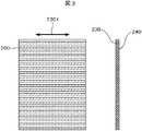
この問題を解決するために、本発明では、図3に示すような対向基板200を使用する。図3の左側は平面図であり、右側は側面図である。図3の対向基板200は、樹脂内にグラスファイバ230を配置するが、このグラスファイバ230は1方向、すなわち黒矢印2301の方向に延在しており、この方向と直角方向に配列している。このような構成の対向基板200では、グラスファイバ230の延在方向とその直角方向では熱膨張に差が生ずる。グラスファイバ230の熱膨張係数は3.8×10⁻⁶/℃であり、使用される樹脂の膨張係数は70〜80×10−6/℃の1/20程度である。 In order to solve this problem, the present invention uses a
なお、繊維としては、グラスファイバ230の他に炭素繊維を使用することが出来る。炭素繊維としては、カーボンナノファイバあるいはカーボンナノチューブを使用することが出来る。グラスファイバ230にしろ炭素繊維にしろ、屈折率は、樹脂材料240の屈折率に近い値であることが望ましい。また、繊維の直径は、可視光透過の妨げとならないように、500nm以下であることが望ましい。樹脂材料240は、アクリル系あるいはエポキシ系の樹脂を使用することが出来る。以上のように、対向基板200の繊維としては、グラスファイバ230でも炭素繊維でもよいが、以後、グラスファイバ230によって代表して説明する。 In addition, as a fiber, carbon fiber other than the
図3において、グラスファイバ230は横方向に整列して延在しているので、横方向の熱膨張係数は小さく、ガラスの熱膨張係数に近い。一方、縦方向、すなわち、グラスファイバ230の延在方向と直角の方向は、樹脂の熱膨張係数に近いので、TFT基板100を構成するガラスの熱膨張係数とは大きく異なることになる。なお、図3では、各グラスファイバ230は完全に横方向に平行に整列しているが、かならずしも、完全平行に配列する必要はなく、一部において、グラスファイバ230が交差してもかまわない。すなわち、概略横方向に整列していればよい。つまり、全体としてグラスファイバ230の延在する方向の熱膨張係数が、その方向と直角な方向の熱膨張係数よりも小さな状態が形成されていれば、本発明の効果を発揮することが出来る。 In FIG. 3, since the
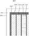
図4と図5は、対向基板200におけるグラスファイバ230の延在方向と、対向基板200に形成されるカラーフィルタ210の延在方向の関係を示す図である。図4において、横方向の黒矢印2301の方向がグラスファイバ230の延在方向である。グラスファイバ230の構成は図4において説明した通りである。図5は、図4に示す対向基板200にカラーフィルタ210およびブラックマトリクス220を形成した状態における平面図である。図5における縦方向の黒矢印2101が、カラーフィルタ210の延在方向である。カラーフィルタ210は縦方向にストライプ状に延在している。図5に示すカラーフィルタ210の延在方向と図4に示すグラスファイバ230の延在方向は直角方向となっている。 4 and 5 are diagrams illustrating the relationship between the extending direction of the
図5において、赤カラーフィルタ210R、緑カラーフィルタ210G、青カラーフィルタ210Bが縦方向に延在し、横方向に配列している。各カラーフィルタ210の間には、ブラックマトリクス220が配置されている。ブラックマトリクスは画面周辺にも形成されている。しかし、図5では、各ストライプ状のカラーフィルタ210内においては、画素120を区別するブラックマトリクスは形成されていない。後で説明するように、本発明の液晶表示装置は、カラーフィルタ210のストライプの方向には、対向基板200とTFT基板100が熱膨張等でずれたとしても、色純度には影響が無い構成となっている。 In FIG. 5, a
図1は、本発明におけるTFT基板100とカラーフィルタ基板600との関係を示す図である。図1において、TFT基板100と対向基板200との間に図示しない液晶が挟持される。図1におけるTFT基板100は、画素120がマトリクス状に形成されている表示領域と端子部140とから形成されている。画素120は画素電極101やTFTを含む概念である。画素120は、図2で説明したように、ガラス基板上に形成され、ガラス基板は、接着材135を介して樹脂基板に接着している。しかし、画素120が形成されている部分のTFT基板100の熱膨張係数はガラスの熱膨張係数に近い。 FIG. 1 is a diagram showing the relationship between the
図1における対向基板200には、カラーフィルタ210がストライプ状に形成されている。赤カラーフィルタ210R、緑カラーフィルタ210G、青カラーフィルタ210Bの間にはブラックマトリクス220が形成されている。図1において、対向基板200はグラスファイバ230が図の黒矢印2301の方向に延在し、これと直角方向に配列している。したがって、対向基板200は横方向、すなわち、黒矢印2301の方向の熱膨張係数は、グラスファイバ230に近い値となっている。一方これと直角の方向、すなわち、縦方向は、樹脂と同程度の熱膨張係数となっている・
この構成においては、液晶表示装置が温度変化した場合、TFT基板100と対向基板200との熱膨張の関係は、横方向と縦方向とで異なることになる。すなわち、黒矢印2301の方向、すなわち、対向基板200においてグラスファイバ230が延在している方向は、TFT基板100と対向基板200との熱膨張の差が小さい。つまり、対向基板200におけるカラーフィルタ210とTFT基板100における画素電極101のずれが小さい。対向基板200の横方向には、異なった色が配置されているが、TFT基板100と対向基板200とのずれが小さいので、色純度が劣化することは無い。In the
In this configuration, when the temperature of the liquid crystal display device changes, the thermal expansion relationship between the
一方、黒矢印2301と直角の方向、すなわち、図1の縦方向では、TFT基板100と対向基板200との熱膨張によるずれが大きい。しかし、図1において、縦方向には、同じ色の画素120が形成されているので、例え、縦方向にずれが生じても色純度が劣化することは無い。また、図1に示すように、各ストライプ状のカラーフィルタ210内には、縦方向に画素を区切るブラックマトリクスは形成されていない。 On the other hand, in the direction perpendicular to the
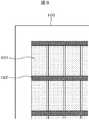
図6は図1に示す本発明の対向基板200の一部拡大図である。図6において、赤カラーフィルタ210R、緑カラーフィルタ210G、青カラーフィルタ210Bがストライプ状に形成されている。各カラーフィルタ210の間にはブラックマトリクス220が縦方向に延在してストライプ状に形成されている。また、カラーフィルタ210R,210G,210Bの周辺には周辺ブラックマトリクス2201が形成されている。しかし、縦方向に画素120を区切るブラックマトリクスは形成されていない。 FIG. 6 is a partially enlarged view of the
図7は従来の対向基板200におけるカラーフィルタ210とブラックマトリクス220の関係を示す平面図である。図7においては、縦方向にも画素を区切るための横方向に延在するブラックマトリクス2202が形成されている。この場合、縦方向にTFT基板100と対向基板200とがずれた場合、横方向に延在するブラックマトリクス2202のために、液晶表示装置の透過率が低下することになる。 FIG. 7 is a plan view showing the relationship between the
なお、図6および図7において、対向基板200の最外周250にはブラックマトリクスは形成されていない。これは、対向基板200とTFT基板100を紫外線硬化樹脂によるシール材によって接着するときに紫外線をシール材に照射できるようにするためである。 6 and 7, the black matrix is not formed on the
図1に戻り、本発明における対向基板200には、ストライプ状の各カラーフィルタ210内には画素120を区切るための横方向へのブラックマトリクス220は形成されていない。したがって、TFT基板100と対向基板200とが熱膨張によってずれるようなことがあっても、それが縦方向のずれである限り、各画素120の透過率が低下することは無い。また、縦方向にずれても、色純度が劣化することも無い。一方、図1において横方向に対向基板200とTFT基板100とがずれを起こすと、色純度も画素120の透過率も劣化するが、この方向は、TFT基板100と対向基板200との熱膨張の差が小さいので、ずれは極めて僅かである。 Returning to FIG. 1, in the
したがって、本発明の構成によれば、対向基板200とTFT基板100との間に熱膨張によるずれが生じても、色純度の劣化を生ずることも、画素120の透過率が低下することも無い。しかし、TFT基板100に形成されたTFT付近には、画素電極101が存在しない。したがって、この部分からバックライトからの光が漏れる可能性があり、この場合は、画像のコントラストを低下させることになる。したがって、TFTが形成された付近はバックライトからの光の遮光を行う必要がある。 Therefore, according to the configuration of the present invention, even if a shift due to thermal expansion occurs between the
図8は、この部分の遮光をするためのTFT基板100の模式平面図である。図8において、画素電極101は図示しない縦方向に延在する映像信号線と横方向に延在する遮光領域102によって囲まれている。なお、映像信号線は図8において、画素電極101を横方向に区画する領域に形成される。TFTは遮光領域102に形成されている。図8のように遮光領域102を形成することによってバックライトからの光漏れを防止することが出来、コントラストを維持することが出来る。 FIG. 8 is a schematic plan view of the
図9は、TN(Twisted Nematic)、VA(Vertical Alignment)等の方式の液晶表示装置において、遮光領域102を形成した状態における具体的画素120の平面図である。TN方式あるいはVA方式は、液晶分子がTFT基板100と対向基板200との間に形成される縦電界によって駆動されるので、縦電界方式の液晶表示装置とも言われる。 FIG. 9 is a plan view of a
図9において、一点鎖線で示した部分は、対向基板200にブラックマトリクス220が形成されている部分なので、この部分からは光は漏れない。また、図9において、横方向には、金属で形成された走査線103が形成されているので、この部分からは光が漏れない。 In FIG. 9, the portion indicated by the alternate long and short dash line is a portion where the
図9において、TFTは省略されているが、TFTのソース電極105と接続するスルーホール104は記載されている。画素電極101には、スルーホール104を介して映像信号が供給される。スルーホール104が形成された部分には、金属で形成されたTFTのソース電極105が形成されているので、この部分からは光は漏れない。 In FIG. 9, although the TFT is omitted, the through
図9において、走査線103、ソース電極105等を覆って、遮光用透明電極1021が形成されている。遮光用透明電極1021には、画素電極101とは異なる電圧が供給される。つまり、遮光用透明電極1021には、対向基板200に形成されている対向電極との関係で、常に光が透過しないような一定電圧が供給される。なお、この一定電圧は、黒表示用の電圧としてすでに存在しているので、遮光用透明電極1021のために特別に電圧を作る必要は無い。 In FIG. 9, a light-shielding
図10は、IPS(In Plane Switching)方式の液晶表示装置において、遮光領域102を形成した状態における具体的画素120の平面図である。IPS方式の液晶表示装置は、液晶分子がTFT基板100と平行な横電界によって駆動されるので、横電界方式液晶表示装置とも呼ばれる。 FIG. 10 is a plan view of a
図10において、一点鎖線で示した部分は、対向基板200にブラックマトリクス220が形成されている部分なので、この部分からは光は漏れない。また、図9において、横方向には、金属で形成された走査線103が形成されているので、この部分からは光が漏れない。 In FIG. 10, the portion indicated by the alternate long and short dash line is a portion where the
IPSも種々の方式が存在するが、図10は、櫛歯状の画素電極101が図示しない平面状に形成された対向電極の上に図示しない絶縁膜を介して形成された構成の方式である。図10において、画素電極101に映像信号が供給されると、櫛歯状電極と、下部に形成された図示しない対向電極との間に形成される電界によって液晶分子が回転することにより液晶層110の透過が制御され、画像が形成される。なお、画素電極101も対向電極も透明電極であるITO(Indium Tin Oxide)によって形成されている。 Although there are various types of IPS, FIG. 10 shows a configuration in which a comb-
このように、IPSでは、画素電極101のエッジ部分において、液晶分子が制御されて液晶層110を透過する光が制御されるが、ITOが存在している部分は、エッジ部を除いて光が遮光される構成となっている。図10においては、画素電極101を遮光領域102にまで形成することによって、液晶によって遮光領域102を形成することが出来る。したがって、IPSにおいては、遮光領域102用の電極を画素電極101と分離して形成する必要は無い。 As described above, in the IPS, the liquid crystal molecules are controlled at the edge portion of the
しかし、図10における画素電極101の下部、すなわち、遮光領域102の上部において、画素電極101と対向電極との間に電界が発生する部分が存在し、この部分では、十分な遮光が出来ない。しがたって、この領域には、スルーホール104部に形成された金属によるソース電極105を拡大して形成することによって遮光膜としている。このように、図10におけるIPSにおいては、画素電極101を縦方向に延在して形成し、かつ、ソース電極105の形状を変化させるだけで、遮光領域102を形成することが出来る。 However, there is a portion where an electric field is generated between the
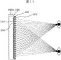
実施例2は、3次元表示装置に本発明を適用した例である。3次元表示装置も種々存在するが、眼鏡を使用しない3次元画像の表示方法として、図11に示すパララックスバリア方式が知られている。図11において、パララックスバリアパネルと呼ばれる複数の縦方向の黒色の細かいバリアが形成された板の後方に平面画像表示装置1000が配置されている。パララックスバリア方式は、平面画像表示装置1000に形成された画像に対し、バリアパターン301によって、右眼用画像320と左眼用画像310を切り取って3次元の画像を形成する方法である。図11において、平面画像表示装置1000は液晶表示装置でもプラズマディスプレイ装置でも有機EL表示装置でもよい。バリアパネルはバリアパターン301の間に透過領域302が形成されている。 Example 2 is an example in which the present invention is applied to a three-dimensional display device. Although various 3D display devices exist, a parallax barrier method shown in FIG. 11 is known as a method for displaying a 3D image without using glasses. In FIG. 11, a flat
図12は、平面画像表示装置1000とバリアパネルを示す分解斜視図である。平面画像表示装置1000には、画素120がマトリクス状に形成されている。バリア基板300には、ストライプ状のバリアパターン301が形成され、バリアパターン301の間が透過領域302となっている。 FIG. 12 is an exploded perspective view showing the flat
平面画像表示装置1000の基板は、一般にはガラスで形成されている。バリア基板300は平面画像表示装置1000に貼り付ける必要がある。図13はガラスで形成されたバリア基板3001を平面画像表示装置1000に貼り付ける状態を示すものである。この場合、平面画像表示装置1000とバリア基板300を接着する際、間に気泡を巻き込みやすい。バリア基板300をフレキシブルな樹脂等で形成することが出来れば、図14で示すような貼り付け方が可能になり、平面画像表示装置1000とバリア基板300との間に気泡を巻き込む危険が小さくなる。 The substrate of the flat
バリア基板300をフレキシブルな樹脂基板で形成する場合、ガラス基板によって形成された平面画像表示装置1000との間の熱膨張の差が問題になる。すなわち、パララックスバリア方式においては、バリア基板300におけるバリアパターン301のピッチと平面画像表示装置1000における画素120のピッチの関係を正確に規定しておく必要がある。熱膨張の差によって、バリアパターン301のピッチと画素120のピッチの関係がずれると、適切な3次元画像を再現することが出来なくなる。 When the
すなわち、パララックスバリア方式においては、バリアパターン301のピッチと画素120ピッチの関係が変わらないようにしておく必要がある。本実施例においては、図3に示すようなグラスファイバ230入りの基板をバリア基板300に使用する。図3に示す基板では、グラスファイバ230の延在方向における熱膨張は、ガラスの熱膨張係数に近く、グラスファイバ230の延在方向と直角の方向は、樹脂の熱膨張係数に近い。したがって、バリア基板300において、バリアパターン301のピッチの方向とグラスファイバ230の延在方向を一致させることによって、熱膨張によるバリアパターン301のピッチと平面画像表示装置1000の画素120のピッチの変動を抑えることが出来る。 That is, in the parallax barrier method, it is necessary to keep the relationship between the pitch of the
図12に戻り、バリア基板300において、バリアパターン301が縦方向に延在し、バリアパターン301の間が透過領域302になっている。バリアパターン301のピッチの方向、すなわち、図12における白矢印2301の方向がバリア基板300におけるグラスファイバ230の延在方向になっている。したがって、バリア基板300における白矢印2301の方向の熱膨張係数はガラスの熱膨張係数に近く、温度が変化しても、平面画像表示装置1000の画素120ピッチとバリアパターン301のピッチとが大きく変動することは無い。一方、バリアパターン301の延在方向は、熱膨張が大きいが、これは、3次元画像形成に影響を与えることは無い。 Returning to FIG. 12, in the
以上のように、バリア基板300に対し、所定の方向にグラスファイバ230を延在させたフレキシブルな樹脂基板を用いることによって、平面画像表示装置1000とバリア基板300の貼り合わせ作業が容易で、かつ、平面画像表示装置1000とバリア基板300の熱膨張の差による3次元画像が劣化することの無い、パララックスバリア方式の3次元画像表示装置を実現することが出来る。 As described above, by using a flexible resin substrate in which the
実施例1は液晶表示装置における対向電極に本発明のフレキシブル基板を適用した例である。本発明のフレキシブル基板は、液晶表示装置に限らず、他の表示装置にも適用することが出来る。図15は有機EL表示装置800に本発明のフレキシブル基板を適用した例である。有機EL表示装置800には、インラインストライプ状に赤、緑、青の画素120が並列して形成されている。有機EL表示装置800は、自発光であり、3色の発光を行うことが可能である。しかし、3色のスペクトルをより純化するために、カラーフィルタ210使用する場合がある。 Example 1 is an example in which the flexible substrate of the present invention is applied to a counter electrode in a liquid crystal display device. The flexible substrate of the present invention can be applied not only to the liquid crystal display device but also to other display devices. FIG. 15 shows an example in which the flexible substrate of the present invention is applied to an organic
図15において、カラーフィルタ210は、カラーフィルタ基板600に形成され、カラーフィルタ基板600を有機EL表示装置800の封止基板500に貼り付ける。この時、カラーフィルタ基板600が樹脂基板のようなフレキシブル基板であれば、貼り付け作業が容易になり、貼り付け作業における歩留まりも向上する。しかし、樹脂基板では、熱膨張係数が大きく、温度が上昇した場合に、カラーフィルタ基板600におけるカラーフィルタ210のピッチと有機EL表示装置800における画素120のピッチが異なることになる。 In FIG. 15, the
そこで、図3に示すような、グラスファイバ230が所定の方向に延在した基板を用いることによって、樹脂基板でありながら、グラスファイバ230の延在した方向の熱膨張係数がガラスに近いカラーフィルタ基板600を得ることが出来る。図15において、白矢印2301が図3に示すグラスファイバ230の延在方向である。したがって、カラーフィルタ基板600におけるカラーフィルタ210のピッチは、図15に白矢印2301の方向での変化は小さい。 Therefore, by using a substrate in which the
なお、図15において、カラーフィルタ基板600におけるカラーフィルタ210は図3等に示すと同様、グラスファイバ230の延在方向とは直角方向にストライプ状に延在している。本発明によって、色純度のよい、かつ、カラーフィルタ210の貼り付け作業の容易な有機EL表示装置を実現することが出来る。 In FIG. 15, the
図15では、光が素子基板400側に出光するいわゆるトップエミッション型の有機EL表示装置であり、カラーフィルタ基板600が素子基板400側に配置されている。しかし、光が素子基板400と反対側に光を出射するいわゆるボトムエミッション型の有機EL表示装置に対しても本発明を適用することが出来る。 15 shows a so-called top emission type organic EL display device in which light is emitted to the
図16は、本発明を電気泳動方式表示装置700に適用した例を示す断面図ある。図16において、電気泳動方式表示装置700にカラーフィルタ基板600が貼り付けられている。電気泳動方式表示装置700では、前面基板と背面基板と隔壁730によって区切られた画素120内に、絶縁性液体740、黒泳動粒子710、および白泳動粒子720が封入されている。黒泳動粒子710と白泳動粒子720には異なった電荷がチャージされている。画素120の上側には例えば、コモン電極750が配置され、画素120の下側には画素電極101が配置されている。画素電極101に印加される電圧によって、画素120の前面基板側に黒泳動粒子710または白泳動粒子720が泳動して付着することによって画像が形成される。 FIG. 16 is a cross-sectional view showing an example in which the present invention is applied to an
このような電気泳動方式表示装置700にカラーフィルタ基板600を配置することによってカラー表示を可能とすることが出来る。この場合も、カラーフィルタ基板600の貼り付けにおける気泡の巻き込み等を防止するためには、カラーフィルタ基板600は樹脂板130のようなフレキシブル基板であることが好ましい。しかし、樹脂基板では、熱膨張係数が電気泳動方式表示装置700のガラス基板の熱膨張係数と異なるので、温度上昇した場合、カラーフィルタ基板600に形成されたカラーフィルタ210のピッチと画素120のピッチがずれる。そうすると画像の再現性を損なったり、輝度が減少したりする。 By disposing the
本実施例では、カラーフィルタ基板600に図3に示すような、グラスファイバ230が所定の方向に延在した基板を使用する。カラーフィルタ基板600において、カラーフィルタ210は所定にピッチでインラインストライプ状に形成されているが、グラスファイバ230の延在方向と、カラーフィルタ210のピッチの方向を一致させることによって、温度が上昇しても、カラーフィルタ210のピッチと電気泳動方式表示装置700における画素120ピッチのずれを小さくすることが出来る。 In the present embodiment, a substrate in which
図16はこの状態を示すものである。図16において、カラーフィルタ基板600が電気泳動方式表示装置700に貼り付けられているが、白矢印2301で示す方向がカラーフィルタ基板600におけるグラスファイバ230の延在方向である。したがって、カラーフィルタ基板600のこの方向への熱膨張は電気泳動方式表示装置700の基板の熱膨張と同程度である。このような構成とすることによって、カラー表示の可能な電気泳動方式表示装置700を歩留まり良く製造することが出来る。 FIG. 16 shows this state. In FIG. 16, the
なお、以上で説明した電気泳動方式表示装置700は白泳動粒子720と黒泳動粒子710を使用するタイプについて説明したが、黒泳動粒子710タイプのみで画像を表示する電気泳動方式表示装置700も存在する。このような電気泳動方式表示装置700の構成は、背面に形成された画素電極101と、隔壁730の表面に形成されたコモン電極との間に電圧を印加することによって、画素電極101に存在する黒泳動粒子710の量によって中間調を表示するものである。この場合、前面基板には、コモン電極は必要無い。このような電気泳動方式表示装置700の場合についても、上記で説明したカラーフィルタ基板600を用いることによって、カラー表示を行うことが出来る。 The
以上の説明では、樹脂基板にはグラスファイバ230が所定の方向に延在しているとして説明したが、グラスファイバ230の代わりに、カーボンナノファイバあるいはカーボンナノチューブ等の炭素繊維が存在していても、以上で説明したような効果を得ることが出来る。 In the above description, the
100…TFT基板、 101…画素電極、 102…遮光領域、 103…走査線、 104…スルーホール、 105…金属電極、 110…液晶層、 120…画素、 125…シール材、 130…樹脂板、 135…接着材、 140…端子部、 200…対向基板、 210…カラーフィルタ、 210R…赤カラーフィルタ、 210G…緑カラーフィルタ、 210B…青カラーフィルタ、 220…ブラックマトリクス、 230…繊維状物質、グラスファイバ、 240…樹脂材料、 250…周辺透過領域、 300…バリア基板、 301…バリアパターン、 302…透過領域、 310…左眼用画像、 320…右眼用画像、 400…素子基板、 500…封止基板、 600…カラーフィルタ基板、 700…電気泳動方式表示装置、 701…背面基板、 701…全面基板、 710…黒泳動粒子、 720…白泳動粒子、 730…隔壁、 740…絶縁性液体、 750…コモン電極、800…有機EL表示装置、 2101…カラーフィルタ延在方向、 2201…周辺ブラックマトリクス、 2202…横方向ブラックマトリクス、 2301…繊維状物質延在方向、 3001…ガラス製バリア基板。 DESCRIPTION OF
Claims (8)
Translated fromJapanese前記対向基板は、グラスファイバまたは炭素繊維が第1の方向に延在し、前記第1の方向と直角方向である第2の方向に配列した樹脂基板であって、前記第2の方向にストライプ状にカラーフィルタが延在して形成され、
前記TFT基板には、前記カラーフィルタの延在方向に沿って、同一の色の画像データを表示する画素が複数形成されていることを特徴とする液晶表示装置。A liquid crystal display device in which liquid crystal is sandwiched between the TFT substrate and the counter substrate, a TFT substrate on which a pixel electrode and a pixel having TFTs are formed, a counter substrate on which a color filter is formed, and the TFT substrate and the counter substrate,
The counter substrate is a resin substrate in which glass fibers or carbon fibers extend in a first direction and are arranged in a second direction perpendicular to the first direction, and stripes in the second direction A color filter is formed to extend in a shape,
A liquid crystal display device, wherein a plurality of pixels for displaying image data of the same color are formed along the extending direction of the color filter on the TFT substrate.
前記対向基板は、グラスファイバまたは炭素繊維が第1の方向に延在し、前記第1の方向と直角方向である第2の方向に配列した樹脂基板であって、前記第2の方向にストライプ状にカラーフィルタが延在して形成され、
前記TFT基板は、樹脂基板に接着材を介してガラス基板が貼り付けられ、前記ガラス基板側に前記TFTおよび前記画素が形成され、
前記ガラス基板には、前記カラーフィルタの延在方向に沿って、同一の色の画像データを表示する画素が複数形成されていることを特徴とする液晶表示装置。A liquid crystal display device in which liquid crystal is sandwiched between the TFT substrate and the counter substrate, a TFT substrate on which a pixel electrode and a pixel having TFTs are formed, a counter substrate on which a color filter is formed, and the TFT substrate and the counter substrate,
The counter substrate is a resin substrate in which glass fibers or carbon fibers extend in a first direction and are arranged in a second direction perpendicular to the first direction, and stripes in the second direction A color filter is formed to extend in a shape,
The TFT substrate has a glass substrate attached to a resin substrate through an adhesive, and the TFT and the pixel are formed on the glass substrate side.
A liquid crystal display device, wherein a plurality of pixels for displaying image data of the same color are formed on the glass substrate along an extending direction of the color filter.
前記カラーフィルタ基板は、グラスファイバまたは炭素繊維が第1の方向に延在し、前記第1の方向と直角方向である第2の方向に配列した樹脂基板であって、前記第2の方向にストライプ状にカラーフィルタが延在して形成され、
前記素子基板には、前記カラーフィルタの延在方向に沿って、同一の色を発光する画素が複数形成されていることを特徴とする有機EL表示装置。An element substrate on which a light emitting element is formed is sealed with a sealing substrate, and the element substrate or the organic EL display device in which a color filter substrate is attached to the sealing substrate,
The color filter substrate is a resin substrate in which glass fibers or carbon fibers extend in a first direction and are arranged in a second direction that is perpendicular to the first direction, in the second direction. A color filter is formed to extend in a stripe shape,
2. The organic EL display device according to claim 1, wherein a plurality of pixels emitting the same color are formed along the extending direction of the color filter on the element substrate.
前記カラーフィルタ基板は、グラスファイバまたは炭素繊維が第1の方向に延在し、前記第1の方向と直角方向である第2の方向に配列した樹脂基板であって、前記第2の方向にストライプ状にカラーフィルタが延在して形成され、
前記画素のうち同一の色を表示する画素が、前記カラーフィルタの延在方向に沿って、複数形成されていることを特徴とする電気泳動方式表示装置。An electrophoretic display device in which pixels having an insulating liquid and electrophoretic particles are formed in a matrix in a region surrounded by a front substrate, a rear substrate, and a partition, and a color filter substrate is attached to the front substrate. ,
The color filter substrate is a resin substrate in which glass fibers or carbon fibers extend in a first direction and are arranged in a second direction that is perpendicular to the first direction, in the second direction. A color filter is formed to extend in a stripe shape,
2. An electrophoretic display device, wherein a plurality of pixels that display the same color among the pixels are formed along an extending direction of the color filter.
前記パララックスバリア基板は、グラスファイバまたは炭素繊維が第1の方向に延在し、前記第1の方向と直角方向である第2の方向に配列した樹脂基板であって、前記第2の方向にストライプ状にバリアパターンが延在して形成されていることを特徴とする3次元表示装置。A three-dimensional display device in which a parallax barrier substrate is attached to a flat image display device,
The parallax barrier substrate is a resin substrate in which glass fibers or carbon fibers extend in a first direction and are arranged in a second direction perpendicular to the first direction, the second direction A three-dimensional display device in which a barrier pattern extends in a stripe shape.
Priority Applications (2)
| Application Number | Priority Date | Filing Date | Title |
|---|---|---|---|
| JP2010225624AJP2012078692A (en) | 2010-10-05 | 2010-10-05 | Display device |
| US13/251,365US20120081643A1 (en) | 2010-10-05 | 2011-10-03 | Display device |
Applications Claiming Priority (1)
| Application Number | Priority Date | Filing Date | Title |
|---|---|---|---|
| JP2010225624AJP2012078692A (en) | 2010-10-05 | 2010-10-05 | Display device |
Publications (1)
| Publication Number | Publication Date |
|---|---|
| JP2012078692Atrue JP2012078692A (en) | 2012-04-19 |
Family
ID=45889531
Family Applications (1)
| Application Number | Title | Priority Date | Filing Date |
|---|---|---|---|
| JP2010225624APendingJP2012078692A (en) | 2010-10-05 | 2010-10-05 | Display device |
Country Status (2)
| Country | Link |
|---|---|
| US (1) | US20120081643A1 (en) |
| JP (1) | JP2012078692A (en) |
Cited By (2)
| Publication number | Priority date | Publication date | Assignee | Title |
|---|---|---|---|---|
| KR20170050732A (en)* | 2015-10-30 | 2017-05-11 | 엘지디스플레이 주식회사 | Flexible display device and fabricating method thereof |
| JP2017207528A (en)* | 2016-05-16 | 2017-11-24 | 株式会社Nsc | Display device manufacturing method |
Families Citing this family (3)
| Publication number | Priority date | Publication date | Assignee | Title |
|---|---|---|---|---|
| JP6425877B2 (en)* | 2013-09-26 | 2018-11-21 | 株式会社ジャパンディスプレイ | Display element and method of manufacturing the same |
| US10423028B2 (en) | 2014-04-22 | 2019-09-24 | E Ink Holdings Inc. | Display apparatus |
| TWI560511B (en) | 2014-04-22 | 2016-12-01 | E Ink Holdings Inc | Electrophoretic display apparatus |
Citations (7)
| Publication number | Priority date | Publication date | Assignee | Title |
|---|---|---|---|---|
| JP2002055334A (en)* | 2000-06-29 | 2002-02-20 | Hynix Semiconductor Inc | Color liquid crystal display device having high aperture ratio |
| JP2003207797A (en)* | 2002-01-17 | 2003-07-25 | Hitachi Ltd | Liquid crystal display device and image display device |
| JP2004205601A (en)* | 2002-12-24 | 2004-07-22 | Seiko Epson Corp | Electro-optical device, manufacturing method of electro-optical device, electronic apparatus |
| JP2004294484A (en)* | 2003-03-25 | 2004-10-21 | Sanyo Electric Co Ltd | Stereoscopic video display device |
| WO2007119409A1 (en)* | 2006-03-31 | 2007-10-25 | Citizen Holdings Co., Ltd. | Large-sized substrate and liquid crystal device employing the large-sized substrate and method for producing the liquid crystal device |
| WO2007144995A1 (en)* | 2006-06-15 | 2007-12-21 | Sharp Kabushiki Kaisha | Display and process for producing the same |
| WO2009130526A2 (en)* | 2008-04-24 | 2009-10-29 | Kodak Graphic Communications Canada Company | Color filter layer alignment |
Family Cites Families (10)
| Publication number | Priority date | Publication date | Assignee | Title |
|---|---|---|---|---|
| TW454101B (en)* | 1995-10-04 | 2001-09-11 | Hitachi Ltd | In-plane field type liquid crystal display device comprising liquid crystal molecules with more than two different kinds of reorientation directions and its manufacturing method |
| KR100405893B1 (en)* | 1995-10-23 | 2004-10-06 | 가부시끼가이샤 히다치 세이사꾸쇼 | Liquid crystal display |
| CN1100279C (en)* | 1996-10-29 | 2003-01-29 | 日本电气株式会社 | Active matrix liquid crystal display screen |
| KR100481593B1 (en)* | 2000-04-21 | 2005-04-08 | 세이코 엡슨 가부시키가이샤 | Electrooptical device |
| JP2004191734A (en)* | 2002-12-12 | 2004-07-08 | Sharp Corp | Plastic substrate and liquid crystal display device having the same |
| JP2004252309A (en)* | 2003-02-21 | 2004-09-09 | Seiko Epson Corp | Electro-optical panel and electronic equipment |
| JP4381782B2 (en)* | 2003-11-18 | 2009-12-09 | 株式会社 日立ディスプレイズ | Liquid crystal display |
| JP4394479B2 (en)* | 2004-02-26 | 2010-01-06 | Nec液晶テクノロジー株式会社 | Liquid crystal display device and manufacturing method thereof |
| US7365815B2 (en)* | 2004-06-16 | 2008-04-29 | Sumitomo Chemical Company, Limited | Phase retardation film and liquid crystal display device including the same |
| EP1843194A1 (en)* | 2006-04-06 | 2007-10-10 | Semiconductor Energy Laboratory Co., Ltd. | Liquid crystal display device, semiconductor device, and electronic appliance |
- 2010
- 2010-10-05JPJP2010225624Apatent/JP2012078692A/enactivePending
- 2011
- 2011-10-03USUS13/251,365patent/US20120081643A1/ennot_activeAbandoned
Patent Citations (8)
| Publication number | Priority date | Publication date | Assignee | Title |
|---|---|---|---|---|
| JP2002055334A (en)* | 2000-06-29 | 2002-02-20 | Hynix Semiconductor Inc | Color liquid crystal display device having high aperture ratio |
| JP2003207797A (en)* | 2002-01-17 | 2003-07-25 | Hitachi Ltd | Liquid crystal display device and image display device |
| JP2004205601A (en)* | 2002-12-24 | 2004-07-22 | Seiko Epson Corp | Electro-optical device, manufacturing method of electro-optical device, electronic apparatus |
| JP2004294484A (en)* | 2003-03-25 | 2004-10-21 | Sanyo Electric Co Ltd | Stereoscopic video display device |
| WO2007119409A1 (en)* | 2006-03-31 | 2007-10-25 | Citizen Holdings Co., Ltd. | Large-sized substrate and liquid crystal device employing the large-sized substrate and method for producing the liquid crystal device |
| WO2007144995A1 (en)* | 2006-06-15 | 2007-12-21 | Sharp Kabushiki Kaisha | Display and process for producing the same |
| WO2009130526A2 (en)* | 2008-04-24 | 2009-10-29 | Kodak Graphic Communications Canada Company | Color filter layer alignment |
| JP2011523081A (en)* | 2008-04-24 | 2011-08-04 | コダック グラフィック コミュニケーションズ カナダ カンパニー | Color filter layer alignment |
Cited By (3)
| Publication number | Priority date | Publication date | Assignee | Title |
|---|---|---|---|---|
| KR20170050732A (en)* | 2015-10-30 | 2017-05-11 | 엘지디스플레이 주식회사 | Flexible display device and fabricating method thereof |
| KR102407529B1 (en) | 2015-10-30 | 2022-06-10 | 엘지디스플레이 주식회사 | Flexible display device and fabricating method thereof |
| JP2017207528A (en)* | 2016-05-16 | 2017-11-24 | 株式会社Nsc | Display device manufacturing method |
Also Published As
| Publication number | Publication date |
|---|---|
| US20120081643A1 (en) | 2012-04-05 |
Similar Documents
| Publication | Publication Date | Title |
|---|---|---|
| JP5550165B2 (en) | Electronic video equipment | |
| JP5156606B2 (en) | Stereoscopic image display device | |
| JP5596625B2 (en) | Display device | |
| US20190089880A1 (en) | Image capturing device | |
| CN107835956B (en) | Parallax barrier with independently controllable areas | |
| US20120120213A1 (en) | Stereoscopic display device | |
| CN102749715B (en) | Display device capable of switching two-dimensional and three-dimensional display modes | |
| CN103424924B (en) | The display device of changeable two dimension and three-dimensional display mode | |
| JP5657508B2 (en) | Liquid crystal display device, electronic device, and optical device | |
| JP2016070949A (en) | Display device | |
| KR20150142891A (en) | 3d display apparatus | |
| KR20130048070A (en) | Display apparatus | |
| CN103154801B (en) | Display device | |
| CN107402473A (en) | Display module and display device | |
| US20120236402A1 (en) | Display device | |
| KR20150032387A (en) | Three-dimension display apparatus | |
| JP2012078692A (en) | Display device | |
| JP2012155307A (en) | Display device | |
| US9105224B2 (en) | Stereoscopic display device | |
| US10056437B2 (en) | Stereoscopic imaging apparatus and user terminal | |
| JP2013235228A (en) | Patterned retarder type image display device having black strips, and manufacturing method therefor | |
| US8570451B2 (en) | Display apparatus and liquid crystal lens | |
| US9606367B2 (en) | Stereoscopic display device | |
| JP2009157301A (en) | Electro-optic device | |
| KR100963872B1 (en) | Flat and three-dimensional display device with a liquid crystal display panel for stereoscopic implementation with wide viewing angle |
Legal Events
| Date | Code | Title | Description |
|---|---|---|---|
| A621 | Written request for application examination | Free format text:JAPANESE INTERMEDIATE CODE: A621 Effective date:20130311 | |
| A977 | Report on retrieval | Free format text:JAPANESE INTERMEDIATE CODE: A971007 Effective date:20130807 | |
| A131 | Notification of reasons for refusal | Free format text:JAPANESE INTERMEDIATE CODE: A131 Effective date:20130820 | |
| A02 | Decision of refusal | Free format text:JAPANESE INTERMEDIATE CODE: A02 Effective date:20131210 |