JP2012078186A - Strain detecting element and blood pressure sensor - Google Patents
Strain detecting element and blood pressure sensorDownload PDFInfo
- Publication number
- JP2012078186A JP2012078186AJP2010223175AJP2010223175AJP2012078186AJP 2012078186 AJP2012078186 AJP 2012078186AJP 2010223175 AJP2010223175 AJP 2010223175AJP 2010223175 AJP2010223175 AJP 2010223175AJP 2012078186 AJP2012078186 AJP 2012078186A
- Authority
- JP
- Japan
- Prior art keywords
- layer
- magnetization
- sensing element
- strain
- magnetization free
- Prior art date
- Legal status (The legal status is an assumption and is not a legal conclusion. Google has not performed a legal analysis and makes no representation as to the accuracy of the status listed.)
- Granted
Links
Images


Classifications
- A—HUMAN NECESSITIES
- A61—MEDICAL OR VETERINARY SCIENCE; HYGIENE
- A61B—DIAGNOSIS; SURGERY; IDENTIFICATION
- A61B5/00—Measuring for diagnostic purposes; Identification of persons
- A61B5/02—Detecting, measuring or recording for evaluating the cardiovascular system, e.g. pulse, heart rate, blood pressure or blood flow
- A61B5/021—Measuring pressure in heart or blood vessels
- A61B5/02108—Measuring pressure in heart or blood vessels from analysis of pulse wave characteristics
- G—PHYSICS
- G01—MEASURING; TESTING
- G01B—MEASURING LENGTH, THICKNESS OR SIMILAR LINEAR DIMENSIONS; MEASURING ANGLES; MEASURING AREAS; MEASURING IRREGULARITIES OF SURFACES OR CONTOURS
- G01B7/00—Measuring arrangements characterised by the use of electric or magnetic techniques
- G01B7/16—Measuring arrangements characterised by the use of electric or magnetic techniques for measuring the deformation in a solid, e.g. by resistance strain gauge
- G01B7/24—Measuring arrangements characterised by the use of electric or magnetic techniques for measuring the deformation in a solid, e.g. by resistance strain gauge using change in magnetic properties
- G—PHYSICS
- G01—MEASURING; TESTING
- G01L—MEASURING FORCE, STRESS, TORQUE, WORK, MECHANICAL POWER, MECHANICAL EFFICIENCY, OR FLUID PRESSURE
- G01L1/00—Measuring force or stress, in general
- G01L1/12—Measuring force or stress, in general by measuring variations in the magnetic properties of materials resulting from the application of stress
- G01L1/125—Measuring force or stress, in general by measuring variations in the magnetic properties of materials resulting from the application of stress by using magnetostrictive means
Landscapes
- Health & Medical Sciences (AREA)
- Life Sciences & Earth Sciences (AREA)
- Physics & Mathematics (AREA)
- Cardiology (AREA)
- General Physics & Mathematics (AREA)
- Heart & Thoracic Surgery (AREA)
- Animal Behavior & Ethology (AREA)
- Pathology (AREA)
- Engineering & Computer Science (AREA)
- Biomedical Technology (AREA)
- Physiology (AREA)
- Medical Informatics (AREA)
- Molecular Biology (AREA)
- Surgery (AREA)
- Biophysics (AREA)
- General Health & Medical Sciences (AREA)
- Public Health (AREA)
- Veterinary Medicine (AREA)
- Vascular Medicine (AREA)
- Hall/Mr Elements (AREA)
- Measuring Fluid Pressure (AREA)
- Measurement Of Length, Angles, Or The Like Using Electric Or Magnetic Means (AREA)
- Transmission And Conversion Of Sensor Element Output (AREA)
Abstract
Description
Translated fromJapanese本発明の実施形態は、歪み検知素子圧力検知素子に関する。Embodiments described herein relate generally to a strain sensing element pressure sensing element.
極薄磁性膜の積層膜で形成されるスピンバルブ膜が知られている。A spin valve film formed of a laminated film of ultrathin magnetic films is known.
スピンバルブ膜は、外部磁界に対して抵抗が変化する。この抵抗変化量は、MR(magnetoresistive)変化率として知られている。MR現象は様々な物理的効果に起因する。巨大磁気抵抗効果(GMR effect: Giant magnetoresistive effect)又はトンネル磁気抵抗効果(TMR: Tunneling magnetoresistive effect)が最も一般的に知られている。The resistance of the spin valve film changes with respect to an external magnetic field. This resistance change amount is known as an MR (magnetoresistive) change rate. MR phenomenon is caused by various physical effects. The giant magnetoresistive effect (GMR effect: Giant magnetoresistive effect) or the tunneling magnetoresistive effect (TMR) is most commonly known.
スピンバルブ膜は、少なくとも2層の強磁性層が、スペーサー層を介して積層された構造から形成される。スピンバルブ膜の磁気抵抗状態は、隣接する強磁性層の磁化方向の相対的な角度によって決まる。一般的な構成では、2つの強磁性層が平行状態のときは、スピンバルブは低い抵抗状態を取り、反平行状態のときには、スピンバルブは高い抵抗状態を取る。隣接する強磁性層の磁化との間の角が中間的な角度の場合には、中間的な抵抗状態になる。The spin valve film is formed of a structure in which at least two ferromagnetic layers are stacked via a spacer layer. The magnetoresistive state of the spin valve film is determined by the relative angle of the magnetization direction of the adjacent ferromagnetic layer. In a general configuration, when two ferromagnetic layers are in a parallel state, the spin valve takes a low resistance state, and when the two ferromagnetic layers are in an antiparallel state, the spin valve takes a high resistance state. When the angle between the magnetizations of adjacent ferromagnetic layers is an intermediate angle, an intermediate resistance state is obtained.
少なくとも二層の磁性層のうち、磁化が容易に回転する磁性層は「磁化自由層」として知られている。磁化が変化しにくい磁性層は「参照層」として知られている。Of the at least two magnetic layers, the magnetic layer whose magnetization easily rotates is known as a “magnetization free layer”. A magnetic layer whose magnetization is difficult to change is known as a “reference layer”.
スピンバルブ膜の抵抗が外部磁界を通じて変化する現象を用いることで、スピンバルブ膜は高感度な磁界検知素子として用いられる。スピンバルブ膜の感度の良い磁界応答の結果として、スピンバルブ膜は広くHDD(Hard Disk Drive)の読み取りヘッドに用いられている。加えて、スピンバルブ膜はMRAM(Magnetic Random Access Memory)のメモリセルとしても用いられている。By using a phenomenon in which the resistance of the spin valve film changes through an external magnetic field, the spin valve film is used as a highly sensitive magnetic field detection element. As a result of the sensitive magnetic field response of spin valve films, spin valve films are widely used in HDD (Hard Disk Drive) read heads. In addition, the spin valve film is used as a memory cell of MRAM (Magnetic Random Access Memory).
外部磁界によって磁化自由層の磁化を変化させるだけでなく、外部歪みによっても磁性層の磁化方向を変化させることができる。係る現象を用いることでスピンバルブ膜は、歪検知素子又は圧力検知素子としてスピンバルブ膜を用いることができる。歪みによる磁化自由層の磁化の変化の物理的な起源は、逆磁歪効果と呼ばれている。係る物理現象の簡単な説明は以下の通りである。Not only can the magnetization of the magnetization free layer be changed by an external magnetic field, but also the magnetization direction of the magnetic layer can be changed by an external strain. By using such a phenomenon, the spin valve film can be used as a strain sensing element or a pressure sensing element. The physical origin of the change in magnetization of the magnetization free layer due to strain is called the inverse magnetostriction effect. A brief explanation of the physical phenomenon is as follows.
磁歪効果は、磁性材料の磁化が変化したときに、磁性材料の歪みが変化する現象である。その歪みの大きさは、磁化の大きさと方向に依存して変化する。従って、歪みの大きさは、これらの磁化の大きさと方向のパラメータを通じて制御できる。また、磁場を印加していったときに歪の量が飽和したときの歪の変化量は磁歪定数λとして知られる。磁歪定数は、磁性材料固有の特性に依存する。The magnetostrictive effect is a phenomenon in which the strain of the magnetic material changes when the magnetization of the magnetic material changes. The magnitude of the distortion varies depending on the magnitude and direction of magnetization. Accordingly, the magnitude of strain can be controlled through these magnitude and direction parameters of magnetization. Further, the amount of change in strain when the amount of strain is saturated when a magnetic field is applied is known as the magnetostriction constant λ. The magnetostriction constant depends on the characteristics unique to the magnetic material.
磁歪効果の逆の現象として、逆磁歪効果も知られている。逆磁歪効果では、外部歪が印加されたときに、磁性材料の磁化が変化する現象である。この変化の大きさは、外部歪みの大きさ及び磁性材料の磁歪定数に依存する。磁歪効果と逆磁歪効果は、物理的に対称な効果なため、逆磁歪効果の磁歪定数は磁歪効果のときの磁歪定数と同じである。An inverse magnetostriction effect is also known as a phenomenon opposite to the magnetostriction effect. The inverse magnetostrictive effect is a phenomenon in which the magnetization of a magnetic material changes when an external strain is applied. The magnitude of this change depends on the magnitude of the external strain and the magnetostriction constant of the magnetic material. Since the magnetostriction effect and the inverse magnetostriction effect are physically symmetric effects, the magnetostriction constant of the inverse magnetostriction effect is the same as the magnetostriction constant of the magnetostriction effect.
磁歪効果と逆磁歪効果には、正の磁歪定数と負の磁歪定数がある。これらの定数は磁性材料に依存する。The magnetostrictive effect and the inverse magnetostrictive effect include a positive magnetostriction constant and a negative magnetostriction constant. These constants depend on the magnetic material.
正の磁歪定数を有する材料の場合、引っ張り歪みが適用された方向に磁化が揃うように変化する。In the case of a material having a positive magnetostriction constant, the magnetization changes in the direction in which the tensile strain is applied.
一方で、負の磁歪定数では逆の場合になる。つまり、圧縮歪みの方向に沿って磁化が変化する。On the other hand, the negative magnetostriction constant is reversed. That is, the magnetization changes along the direction of compressive strain.
逆磁歪効果はスピンバルブ膜の磁化自由層の磁化方向を変化させるために用いることができる。外部歪が印加されると、逆磁歪効果によって磁化自由層の磁化方向が変化するため、参照層と磁化自由層の相対的磁化角度に差が生じる。これによって、スピンバルブ膜の抵抗が変化する。つまり、歪検知素子として用いることが可能となる。The inverse magnetostrictive effect can be used to change the magnetization direction of the magnetization free layer of the spin valve film. When an external strain is applied, the magnetization direction of the magnetization free layer changes due to the inverse magnetostriction effect, so that a difference occurs in the relative magnetization angle between the reference layer and the magnetization free layer. As a result, the resistance of the spin valve film changes. That is, it can be used as a strain sensing element.
前述のように、歪みを感知することができるスピンバルブ膜の抵抗変化量は歪みが適用される方向に依存する。As described above, the resistance change amount of the spin valve film that can sense the strain depends on the direction in which the strain is applied.
正の磁歪定数を有する磁化自由層おいて、引っ張り応力を磁化容易軸に沿って適用すると、磁化の変化は生じない。これは、既に低エネルギー状態にあるからである。つまり、圧縮応力のときのみ、敏感に検知することが可能となる。When a tensile stress is applied along the easy axis in a magnetization free layer having a positive magnetostriction constant, no change in magnetization occurs. This is because it is already in a low energy state. That is, it becomes possible to detect sensitively only in the case of compressive stress.
一方、負の磁歪定数を有する磁化自由層においては、圧縮応力を磁化自由層に適用すると、磁化の変化は生じない。これは、既に低エネルギー状態にあるからである。つまり、引っ張り応力のときのみ、敏感に検知することが可能となる。
しかしながら、一般的に外部から圧力が印加されたとき、各部位によって応力状態は異なる。つまり、ある箇所では圧縮応力となり、ある箇所では引っ張り応力となる。すると、あるスピンバルブ膜を用いたときに、圧縮応力か引っ張り応力かのいずれかひとつのみしか、外部応力を敏感に検知することができない。これは、歪検知素子、圧力検知素子として考えたときに、感度良く検知することの実現を大きく阻むものである。On the other hand, in a magnetization free layer having a negative magnetostriction constant, no change in magnetization occurs when compressive stress is applied to the magnetization free layer. This is because it is already in a low energy state. That is, it becomes possible to detect sensitively only in the case of tensile stress.
However, in general, when pressure is applied from the outside, the stress state differs depending on each part. That is, it becomes a compressive stress at a certain location and a tensile stress at a certain location. Then, when a certain spin valve film is used, only one of the compressive stress and the tensile stress can sensitively detect the external stress. This greatly hinders the realization of sensitive detection when considered as a strain sensing element and a pressure sensing element.
本発明の実施形態は、前述のような課題を克服するために、良好な感度の歪検知素子、圧力検知素子を実現するためのスピンバルブ膜構造の改善に関する。An embodiment of the present invention relates to an improvement in a spin valve film structure for realizing a strain sensing element and a pressure sensing element with good sensitivity in order to overcome the above-described problems.
本発明の一態様に係る歪検知素子、または圧力検知素子は、磁化方向が変化可能で、外部歪が印加されていない状態では膜面垂直の磁化方向を有する磁化自由層と、磁化を有する参照層と、前記磁化自由層と前記参照層との間に設けられたスペーサー層と、を備えた積層体と、前記積層体の積層面に対して垂直方向に通電する一対の電極と、前記一対の電極の何れか一方に設けられた基板と、前記基板が歪むと、前記磁化自由層の磁化の回転角度と前記参照層の磁化の回転角度が異なることを特徴とする。A strain sensing element or a pressure sensing element according to one embodiment of the present invention has a magnetization free layer having a magnetization direction perpendicular to a film surface in a state in which the magnetization direction can be changed and no external strain is applied, and a reference having magnetization A laminated body comprising a layer, a spacer layer provided between the magnetization free layer and the reference layer, a pair of electrodes for energizing in a direction perpendicular to a laminated surface of the laminated body, and the pair When the substrate provided on any one of the electrodes and the substrate are distorted, the magnetization rotation angle of the magnetization free layer and the magnetization rotation angle of the reference layer are different.
以下図面を参照して、本発明の各実施形態を説明する。同じ符号が付されているものは同様のものを示す。なお、図面は模式的または概念的なものであり、各部分の厚みと幅との関係、部分間の大きさの比係数などは、必ずしも現実のものと同一とは限らない。また、同じ部分を表す場合であっても、図面により互いの寸法や比係数が異なって表される場合もある。Embodiments of the present invention will be described below with reference to the drawings. The same reference numerals denote the same items. Note that the drawings are schematic or conceptual, and the relationship between the thickness and width of each part, the ratio coefficient of the size between the parts, and the like are not necessarily the same as actual ones. Further, even when the same part is represented, the dimensions and ratio coefficient may be represented differently depending on the drawing.
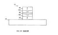
発明の実施形態として、2種類の実施形態がある。一つ目は、歪検知素子、二つ目は圧力検知素子である。歪検知素子は、基板の圧縮応力、引っ張り応力を測定する素子である。典型的には図1のように、基板の上にスピンバルブ膜が形成されていれば、歪検知素子として機能する。二つ目の圧力検知素子は、歪検知素子が「メンブレン」の上に形成された、メンブレンまで含めた素子のことである。メンブレンが圧力から歪への変換を行う鼓膜のような役割を果たす。つまり、圧力検知素子という場合には、必ず歪検知素子をそのなかに含有した構造となる。本発明は、歪検知素子のスピンバルブ膜構造に関する発明なため、歪検知素子、圧力検知素子、いずれの場合においても効果を発揮する発明である。There are two types of embodiments of the invention. The first is a strain sensing element and the second is a pressure sensing element. The strain sensing element is an element that measures the compressive stress and tensile stress of the substrate. Typically, as shown in FIG. 1, if a spin valve film is formed on a substrate, it functions as a strain sensing element. The second pressure sensing element is an element including the membrane in which the strain sensing element is formed on the “membrane”. The membrane acts like an eardrum that converts pressure to strain. That is, in the case of a pressure detection element, the structure always includes a strain detection element. Since the present invention is an invention related to the spin valve film structure of the strain sensing element, the invention is effective in any case of the strain sensing element and the pressure sensing element.
圧力検知素子はさらに二つに分類できる。一つ目は、従来のSi等で形成されたメンブレンを用いた圧力検知素子である。二つ目は、従来のSiとは異なる材料によってメンブレンを構成した圧力検知素子である。本発明は、Siで形成されたメンブレンを用いた素子構造においても効果を発揮するが、Si以外の新たな材料、構造でメンブレンが形成された素子構造においても効果を発揮する。There are two types of pressure sensing elements. The first is a pressure sensing element using a membrane made of conventional Si or the like. The second is a pressure sensing element whose membrane is made of a material different from conventional Si. The present invention is effective even in an element structure using a membrane formed of Si, but is also effective in an element structure in which a membrane is formed of a new material or structure other than Si.
典型的な実施例として、従来のSiで形成されたメンブレンを用いた検知素子について発明の実施形態の要点を説明する。次に、従来のSi以外の材料で形成されたメンブレンを用いた場合の実施形態について説明する。As a typical example, the gist of an embodiment of the present invention will be described with respect to a sensing element using a conventional membrane formed of Si. Next, an embodiment in which a membrane formed of a material other than conventional Si is used will be described.
メンブレンは、圧力から機械的な歪への変換のために用いられる鼓膜のようなものである。外部から圧力を印加したときに、メンブレンの設計、およびメンブレンの位置に依存して、異なる大きさの歪みが生じる。このようなメンブレンの位置に依存した歪は、メンブレン上に各位置に歪検知素子を形成することで圧力を検知することが可能となる。メンブレン上の各位置の歪をすべて歪検知素子で検知できると、圧力検知素子の性能として、非常に良好になる。しかしながら、前述のように、スピンバルブ膜を用いた歪検知素子では、検知可能な歪と、検知不可能な歪が発生してしまう。The membrane is like the eardrum used for the conversion from pressure to mechanical strain. When pressure is applied from the outside, different magnitudes of distortion occur depending on the membrane design and the position of the membrane. The strain depending on the position of the membrane can be detected by forming a strain detecting element at each position on the membrane. If all the strain at each position on the membrane can be detected by the strain sensing element, the performance of the pressure sensing element becomes very good. However, as described above, in a strain sensing element using a spin valve film, a detectable strain and a non-detectable strain are generated.
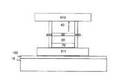
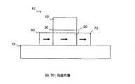
図1Aと図1Bは、歪検知素子10を示す。歪検知素子10は、基板15の上に、参照層20と、スペーサー層30と、磁化自由層40とを備えたスピンバルブ膜構造が形成されている。参照層20、および磁化自由層40は磁性材料で形成される。スペーサー層30は、基本的には非磁性材料からなる。しかし、後述するように、磁性材料もスペーサーとして機能するものに関して用いることができる。スピンバルブ膜に電流を流すために、一対の電極が用いられる。CIP(Current−in−plane)配置では、図1Aのように一対の電極501、502が用いられる。CPP(Current−perpendicular−to−plane)配置では、図1Bのように一対の電極511、512が用いられる。スピンバルブ膜から基板への電流を絶縁する目的や、基板表面の荒れを緩和するために、コーティング層150がCIP配置とCPP配置の両方に用いられる。参照層20/スペーサー層30/磁化自由層40の積層膜の下地として、下地層70を用いる。以下、それぞれの部分について詳細に説明する。積層体は参照層20、スペーサー層30、及び磁化自由層40で定義される。1A and 1B show a
参照層20の目的は磁化自由層40の磁化を「参照」することである。この機能のために、歪みが印加されたときの参照層20の磁化の状態は、磁化自由層40の磁化の状態とは異なる。実施形態の一つは、参照層20の磁化が外部歪みに関わらず固定されていることである。参照層が面内磁化を有する場合、IrMn又はPtMnのようなピニング層(後述)が参照層20の下に用いられる。このような単純なピニング構造の代わりに、参照層/Ru0.9nm/磁性層/ピニング層というシンセティック構造を用いても良い。参照層がハードな磁性膜からなる場合、つまり外部歪が印加されても参照層の磁化方向が変化しない場合には、ピニング層を省略してもよい。The purpose of the
また、参照層20の磁化は必ずしも外部歪が印加されたときに固着されている必要は無い。なぜなら、外部歪が印加されたときの参照層20の磁化変化が磁化自由層と異なりさえすれば、参照層と磁化自由層の相対磁化角度は外部歪に依存するため、外部歪を検知することが可能となるからである。参照層20は磁性材料で形成されるため、少なくともFe、Co、又はNiのいずれか一つの元素を含んでいる。なお、参照層の磁化は基板15が歪んでいない場合に固定されている。Further, the magnetization of the
スペーサー層30は、MR現象の物理的な効果に依存して、数種類のバリエーションを有している。MR現象としてTMR効果を用いる場合、MgOような材料が、典型的な材料として用いられる。Al、Ti、Zn、Si、Hf、Ta、Mo、Wo、Nb、Cr、Mg、又はZrに基づく酸化物、窒化物、または酸窒化物も用いることができる。MR現象としてGMR効果を用いる場合、CIP配置でもCPP配置でもスペーサー層30は、Cu、Au、Ag、Au、又はCrのような金属材料を用いることができる。このような単純金属層だけでなく、CPP配置の場合には、電流狭窄(CCP: Current-Confined-Path)スペーサーを用いることもできる。CCPスペーサーには、絶縁層を上限に貫通する複数のナノオーダーのメタルパスが用いられる。CCPスペーサーを用いることの利点は、MR効果を高めるだけでなく、抵抗の大きさも制御することが可能なことである。CCPスペーサーのメタルパス材料としては、単純金属スペーサーの材料群と同じCu、Au、Ag、Al、又はCrなどであり、絶縁層はAl、Ti、Zn、Si、Hf、Ta、Mo、Wo、Nb、Cr、Mg、又はZrに基づく酸化物、窒化物、又は酸窒化物からなる。The
磁化自由層40の特徴は、外部歪みがない状態においては、磁化自由層40の磁化方向が膜面に対し略垂直方向に向いていることである。ここが本発明において最も重要な特徴的な構造である。その様子を図1A及び図1Bに示す。この図では、磁化の方向は上向き矢印であるが、下向き矢印も同様に用いることができる。The characteristic of the magnetization
膜面に対し垂直な方向に磁化を有する磁性層をスピンバルブ膜に用いることは、MRAM(Magnetic Random Access Memory)又はSTO(Spin Torque Oscillator)でも研究レベルで検討はされている。しかしながら、本発明において膜面垂直方向の磁化を用いる効果は、MRAM、STOなどとは全く異なる。MRAMの場合、膜面垂直磁化の磁性層のタイプが開発されている理由は、高密度化に有利なためである。メモリの場合、微細化に対するスケーリングが成立しなければならないため、微細化したときの磁化方向が安定である必要がある。膜面内に磁化方向が向いている場合、微細化に伴い反磁界が大きくなってしまうため、磁化を保つことがエネルギー的に不利となり、実現が難しくなる。つまり、メモリとしてのスケーリング則が成立しなくなってしまう。そのため、スケーリングが成立する高密度化のために、膜面垂直磁化が研究検討されている。この事情は、最近のHDDで既に実用化されている、磁気記録媒体において垂直磁気記録(PMR: Perpendicular Magnetic Recording)を用いる理由と全く同じである。The use of a magnetic layer having magnetization in a direction perpendicular to the film surface as a spin valve film has been studied at the research level in MRAM (Magnetic Random Access Memory) or STO (Spin Torque Oscillator). However, the effect of using the magnetization in the direction perpendicular to the film surface in the present invention is completely different from that of MRAM, STO, and the like. In the case of MRAM, the reason for the development of the perpendicularly magnetized magnetic layer type is that it is advantageous for high density. In the case of a memory, since scaling for miniaturization must be established, the magnetization direction when miniaturized needs to be stable. When the magnetization direction is in the film plane, the demagnetizing field is increased with the miniaturization, so that maintaining the magnetization is disadvantageous in terms of energy and difficult to realize. That is, the scaling rule as a memory is not established. For this reason, film surface perpendicular magnetization has been studied for the purpose of increasing the density to achieve scaling. This situation is exactly the same as the reason why perpendicular magnetic recording (PMR) is used in a magnetic recording medium that has already been put to practical use in recent HDDs.
STOの応用についても、膜面に対し垂直な磁気異方性を有する磁性層を用いた膜構成が研究されている。この理由は、STOとして動作させるときには素子サイズを微小にしなければ良好な発振特性が得られないため、微細化された素子において磁化が安定な膜面垂直な磁気異方性を用いるほうが安定なためである。つまり、スケーリング則という観点ではないものの、微細化した素子で形成するときには膜面垂直方向の磁化を有することが有利という点で、MRAMと同様の理由である。また、二点目として、膜面垂直な磁気異方性を有する材料のほうが、より大きな磁気異方性を有する材料があるためである。大きな磁気異方性のほうが、STOとしての発振周波数を向上させることが可能となるため、大きな発振周波数を得ようとした場合には、膜面垂直な磁気異方性材料のほうが有利になるためである。Regarding the application of STO, a film configuration using a magnetic layer having a magnetic anisotropy perpendicular to the film surface has been studied. The reason for this is that when operating as an STO, good oscillation characteristics cannot be obtained unless the element size is made small, so it is more stable to use magnetic anisotropy perpendicular to the film surface where the magnetization is stable in a miniaturized element. It is. In other words, although it is not a viewpoint of scaling law, it is the same reason as MRAM in that it is advantageous to have magnetization in the direction perpendicular to the film surface when forming with a miniaturized element. The second point is that a material having a magnetic anisotropy perpendicular to the film surface has a material having a larger magnetic anisotropy. Since large magnetic anisotropy can improve the oscillation frequency as STO, the magnetic anisotropy material perpendicular to the film surface is more advantageous when trying to obtain a large oscillation frequency. It is.
上記2つのMRAM,STOに対し、本発明のように歪みセンサ・圧力検知素子に垂直異方性を用いることの効果は全く異なる。前述したように、メンブレン内の歪検知素子が受ける実際の歪みは、配置位置によっても異なり、非常に複雑である。圧縮応力か引っ張り応力かという、極性の違いさえ、メンブレンの位置に依存して生じるうる。このような状態では、面内磁化を有する磁化自由層では抵抗の変化として検知できない場合もあり、検知に関するSNR(Signal to Noise Ratio)劣化を引き起こす原因になる。一方、膜面垂直磁化を有する磁化自由層40の場合、図1C、図1Dに示すように抵抗変化を検知することができる。つまり、理想的な測定環境のみでしか測定できなかったのに対し、測定環境に対して高感度でロバストな、歪検知素子、圧力検知素子を実現することができる。つまり、引っ張り応力、圧縮応力いずれの場合においても、膜面垂直方向の磁化を有する磁化自由層を用いれば、歪を検知可能となる。これは、膜面内に磁化を有する磁化自由層を用いている場合には実現できない。また、この効果は、MRAM、STOにおいて膜面垂直方向の磁化を有する磁性層を用いる理由とは全く異なる。The effect of using vertical anisotropy for the strain sensor and pressure sensing element as in the present invention is completely different from the above two MRAM and STO. As described above, the actual strain received by the strain sensing element in the membrane varies depending on the arrangement position and is very complicated. Even a difference in polarity, whether compressive or tensile, can occur depending on the position of the membrane. In such a state, the magnetization free layer having in-plane magnetization may not be detected as a change in resistance, which causes a SNR (Signal to Noise Ratio) deterioration related to detection. On the other hand, in the case of the magnetization
それゆえに、外部歪に対して磁化方向が変化する磁性層である、磁化自由層に垂直異方性が必要となる。一方で、MRAMの場合、面内垂直異方性は磁化自由層と参照層の両方に必ず用いなければ意味がない。これは、参照層が膜面内の磁化を有していては、反磁界の問題が結局生じてしまうからである。これは、垂直異方性を用いる理由が異なっているためである。
また、垂直磁気異方性の磁化自由層を用いる理由が従来のMRAMなどと異なることによって、さらに構成の違いが生じる。その詳細を以下に説明する。Therefore, perpendicular anisotropy is required for the magnetization free layer, which is a magnetic layer whose magnetization direction changes with respect to external strain. On the other hand, in the case of MRAM, in-plane perpendicular anisotropy is meaningless unless it is always used for both the magnetization free layer and the reference layer. This is because if the reference layer has in-plane magnetization, the problem of demagnetizing fields will eventually occur. This is because the reason for using vertical anisotropy is different.
Further, the reason for using the perpendicular magnetic anisotropy magnetization free layer is different from that of a conventional MRAM or the like, which further causes a difference in configuration. Details thereof will be described below.
磁界の書き込みによるMRAMの場合、磁化自由層の磁化は外部磁界、もしくはスピン注入電流によって駆動させる。こうした原理によって駆動する場合、他のアーティファクトで磁化方向が変化するのは望ましくないため、磁化自由層の良好な軟磁性の実現が必要となる。より具体的には、磁性層の磁歪定数を小さくすることは必須要件となる。この状況は、STOでも同様であり、スピン注入電流によって発振を駆動する素子なため、素子に加わる応力、歪で磁化自由層の磁化が変化することは根本的な動作に影響を与える。そのため、磁性層の磁歪定数を小さくすることは必須要件となる、特に、小さな素子サイズの場合、製造工程において引き起こされる歪みの大きさが大きくなるため、小さい磁歪定数の磁性層を用いることはより必須要件となる。具体的には、磁歪定数の絶対値は少なくとも10−6よりも小さくする必要がある。このような磁歪定数の絶対値の制約は、HDDの読み取りヘッドでも存在し、磁歪定数の絶対値は10−6よりも小さくする必要がある。In the case of an MRAM by magnetic field writing, the magnetization of the magnetization free layer is driven by an external magnetic field or a spin injection current. When driven by such a principle, it is not desirable for the magnetization direction to change due to other artifacts, so it is necessary to realize good soft magnetism in the magnetization free layer. More specifically, it is an essential requirement to reduce the magnetostriction constant of the magnetic layer. This situation is the same in STO, and since it is an element that drives oscillation by a spin injection current, the change in the magnetization of the magnetization free layer due to stress and strain applied to the element affects the fundamental operation. Therefore, it is an essential requirement to reduce the magnetostriction constant of the magnetic layer. Particularly, in the case of a small element size, since the magnitude of strain caused in the manufacturing process increases, it is more necessary to use a magnetic layer having a small magnetostriction constant. It is an essential requirement. Specifically, the absolute value of the magnetostriction constant needs to be smaller than at least 10−6 . Such restrictions on the absolute value of the magnetostriction constant also exist in the HDD read head, and the absolute value of the magnetostriction constant needs to be smaller than 10−6 .
一方、歪み又は圧力のセンサでは、磁歪定数は外部歪みによって磁化の変化を実現するために、MRAM、STOとは全く逆に、大きい値である必要がある。この必要とされる磁歪定数は下記のように説明される。
磁気弾性エネルギーと静磁エネルギーとのエネルギーバランスで、以下の式のように記載される。On the other hand, in a strain or pressure sensor, the magnetostriction constant needs to be a large value, contrary to MRAM and STO, in order to realize a change in magnetization due to external strain. This required magnetostriction constant is explained as follows.
The energy balance between magnetoelastic energy and magnetostatic energy is described by the following equation.
(1/2)ΔHkBs=(3/2)Δσλ ・・・(1)(1/2) ΔHk Bs = (3/2) Δσλ (1)
ΔHkは外部歪を印加することに伴う磁化自由層の磁化の変化であり、Bsは磁化自由層の飽和磁化、Δσは外部から与えられた歪み、λは磁化自由層の磁歪定数である。この式から、あるΔσが与えられたときに、ΔHkの変化を大きくするためには、磁化自由層の磁歪λを大きくする必要があることがわかる。この必要性は、明らかにHDD、MRAM、STOなどの応用とはまったく逆の必要要件である。前述したように、HDDヘッド、MRAM、及びSTO応用は、磁歪定数の絶対値として10−6よりも小さなλが必要である。しかしながら、そのような小さなλでは歪み検知には応用できない。なぜなら、磁歪定数の絶対値が10−6以下という値は、素子加工などによって生じる外部歪が生じても、スピンバルブ膜の磁化自由層の磁化方向を変化させるほどの逆磁歪効果を発生させないために現状のHDD、MRAM、STOなどの必要スペックとなっている。つまり、本発明のように歪検知素子として考えるときには、充分な逆磁歪効果を発現しないため、歪検知素子としては機能しないことを意味するからである。ΔHk is a change in magnetization of the magnetization free layer accompanying application of external strain, Bs is saturation magnetization of the magnetization free layer, Δσ is strain applied from the outside, and λ is a magnetostriction constant of the magnetization free layer. . From this equation, it can be seen that in order to increase the change in ΔHk when a certain Δσ is given, it is necessary to increase the magnetostriction λ of the magnetization free layer. This need is clearly a requirement that is completely opposite to applications such as HDD, MRAM, and STO. As described above, HDD head, MRAM, and STO applications require λ smaller than 10−6 as the absolute value of magnetostriction constant. However, such a small λ cannot be applied to distortion detection. This is because an absolute value of the magnetostriction constant of 10−6 or less does not generate an inverse magnetostriction effect that changes the magnetization direction of the magnetization free layer of the spin valve film even if an external strain occurs due to element processing or the like. In addition, current specifications such as HDD, MRAM, and STO are required. That is, when it is considered as a strain sensing element as in the present invention, it does not function as a strain sensing element because it does not exhibit a sufficient inverse magnetostriction effect.
また、別の理由として、膜面垂直の磁気異方性を有する材料の場合、面内磁化を有する軟磁性材料とは異なり、磁気異方性の大きさは大きい。その理由は、大きな磁気異方性を有しないと、膜面内に磁化が向くことが有利な、形状異方性に打ち勝つことができないためである。このような大きな磁気異方性をもつ磁性層を用いるということは、(1)式におけるHkが大きい材料を用いるということを意味する。つまり、外部歪が印加されていない状態において大きなHkをもつ磁化自由層のHkを外部歪によって変化させて検知するには、ΔHkの値として、充分大きな変化量を発生させないと、変化量として検知できないことになる。つまり、ΔHkを通常の膜面内に磁化を有する磁化自由層を用いる場合よりもさらに大きなΔHkを発生させる必要がでてくる。すなわち、(1)式からわかるように、より大きなλの磁化自由層を用いることが必須となる。小さな磁歪定数λめられる従来の応用と比較すると、歪検知素子として用いる本発明の場合には、少なくとも磁歪定数の絶対値が10-6よりも大きなλは必須となる。より好ましくは、磁化自由層の磁歪定数の絶対値は10-5よりも大きな値を有することが必要とされる。As another reason, in the case of a material having magnetic anisotropy perpendicular to the film surface, the magnitude of magnetic anisotropy is large, unlike a soft magnetic material having in-plane magnetization. The reason is that without a large magnetic anisotropy, it is not possible to overcome the shape anisotropy, which is advantageous in that the magnetization is oriented in the film plane. Using a magnetic layer having such a large magnetic anisotropy means using a material having a large Hk in the equation (1). In other words, in order to detect the change of the Hk of the magnetization free layer having a large Hk by the external strain when no external strain is applied, the change is detected as a change amount unless a sufficiently large change amount is generated as the value of ΔHk. It will not be possible. That is, it is necessary to generate a larger ΔHk than when a magnetization free layer having magnetization in the normal film plane is used. That is, as can be seen from the equation (1), it is essential to use a larger magnetization free layer of λ. Compared with a conventional application in which a small magnetostriction constant λ is required, in the present invention used as a strain sensing element, at least an absolute value of the magnetostriction constant greater than 10−6 is essential. More preferably, the absolute value of the magnetostriction constant of the magnetization free layer is required to have a value larger than 10−5 .
スピンバルブ膜膜の成膜の順序としては、参照層20/スペーサー層30/磁化自由層40(参照層が下側に存在しているので「ボトムタイプ」と呼ばれる)又は磁化自由層40/スペーサー層30/参照層20(参照層が上側に存在しているので「トップタイプ」と呼ばれる)のどちらでも用いることができる。図1A,図1Bにおいてはボトム型における実施例を示しているが、本発明の本質的な効果としては、ボトム型でもトップ型でも違いは発生せず、同等である。The order of film formation of the spin valve film is as follows:
参照層20/スペーサー層30/磁化自由層40のボトム型又は磁化自由層40/スペーサー層30/参照層20トップ型のいずれの場合でも下地層70が用いられる。本明細書において「下地層」という言葉は、広い概念を含んで用いる。「下地層」はバッファ層、シード層、又はピニング層(図示せず)のような多層からなる。いくつかのこれらの層は特有の膜構造に依存して省略されていてもよい。バッファ層は、フレキシブル基板から生じる荒れのような予期せぬ効果を避けるために用いられる。コーティング層150でバッファ効果が充分な場合は、下地層におけるバッファ層は省略できる。シード層は、参照層20/スペーサー層30/磁化自由層40又は磁化自由層40/スペーサー層30/参照層20の結晶配向性を制御するために用いられる。ピニング層は必要であれば参照層の磁化を固定するために用いられる。The
スピンバルブ膜50は、参照層20、スペーサー層30、及び磁化自由層40から構成される。外部歪み又は圧力による抵抗変化を検知するためにスピンバルブ膜50に対してセンス電流を通電させる必要であるので、電極はスピンバルブ膜50に設けられていなければならない。これは、発明の実施形態として最低限必要な要素となる。The
より詳細には、電極を有するスピンバルブ膜50は図1A及び図1Bに示されている。More specifically, a
図1Aでは、スピンバルブ膜50はCIPスピンバルブ(面内通電)、スピンバルブ膜の側面に設けられた一対の電極501、502から構成される。基板15に対するスピンバルブ膜50からのリーク電流漏避けるために、絶縁コーティング層150はスピンバルブ膜50と基板15との間に用いられる。In FIG. 1A, the
電極501、502において、ハードバイアス(硬磁性材料)が磁化自由層40のシングルドメインを実現するために用いられる(図示せず)。In the
図1Bでは、スピンバルブ膜50はCPP−GMR膜又はTMR膜のようなCPPスピンバルブ(面直通電)から構成される。スピンバルブ膜50に電流を供給するために、下部電極511及び上部電極512が使用される。基板15に対するスピンバルブ膜50からの電流漏れを避けるために、絶縁コーティング層150がスピンバルブ膜50と基板15との間に用いられる。CPPスピンバルブ膜の場合、絶縁膜600がスピンバルブ膜50の側面に使用される必要がある。In FIG. 1B, the
リソグラフィー技術を用いることで、基板上における下部電極511との電気的な接触は、上部電極512との電気的な接触と同様に実現できる。ここは従来技術で形成できるため、詳細は割愛する。By using the lithography technique, electrical contact with the
絶縁膜600の一方の側では、ハードバイアス(硬磁性材料)が磁化自由層のシングルドメインを実現するために用いられる(図示せず)。On one side of the insulating
図1A及び図1Bに示すように、電極はCIPとCPPのスピンバルブ構成との間で異なるが、本発明における特徴である磁化自由層、その他動作原理における説明は基本的に同様である。それゆえに、電極の描写は以後の描写及び図から省略して説明する。
(第1の実施形態)As shown in FIGS. 1A and 1B, the electrodes differ between the CIP and CPP spin valve configurations, but the description of the magnetization free layer, which is a feature of the present invention, and other operating principles is basically the same. Therefore, the description of the electrode will be omitted from the following description and drawings.
(First embodiment)
発明の第1の実施形態は図1Bのスピンバルブ膜を用いることで示されている。基板15は、たとえばSiから構成され、Siを用いた場合はメンブレン構造は基板の一部を薄膜化して形成する。その薄膜化された構造は図11Aの実施例で示したものとほぼ同様であり、基板の一部が薄膜化された構造になっており、その薄膜化された基板の上にスピンバルブ膜が形成されている。しかしながら、外部歪によって曲がる部分が形成され、その上にスピンバルブ膜が形成されるのならば、Si以外の材料でも形成可能である。たとえば、後で説明するようにフレキシブル基板を用いることも可能である。A first embodiment of the invention is shown using the spin valve film of FIG. 1B. The
基板15は、Siで形成されたメンブレン、または曲がりやすい材料を用いたフレキシブル基板である。フレキシブル基板の例として、ポリマー材料などが用いられる。ポリマー材料として以下のような例が挙げられる。たとえば、アクリロニトリルブラジエンスチレン、シクロオレフィンポリマー、弾性を有するエチレンプロピレン、ポリアミド、ポリアミド-イミド、ポリベンジルイミダゾール、ポリブチレンテレフタレート、ポリカーボネート、ポリエチレン、ポリエチレンエーテルケトン、ポリエチルイミド、ポリエチレンイミン、ポリエチレンナフタレン、ポリエステル、ポリサルフォン、ポリエチレンテレフタレート、フェノールホルムアルデヒド、ポリイミド、ポリメチルメタクリレート、ポリメチルペンテン、ポリオキシメチレン、ポリプロピレン、m−フェニルエーテル、ポリp−フェニルサルファイド、p−アミド、ポリスチレン、ポリサルフォン、ポリビニルクロライド、ポリテトラフルオロエテン、パーフルオロアルコキシ、フッ化エチレンプロピレン、ポリテトラフルオロエテン、ポリエチレンテトラフルオロエチレン、ポリエチレンクロロトリフルオエチレン、ポリビニリデンフルオライド、メラミンホルムアルデヒド、液晶性ポリマー、又は尿中ホルムアルデヒドを用いることができる。The
コーティング層150は、ポリメチルメタクリレート又はポリp−フェニレンサルファイドのような有機材料、又はAl2O3又はSiO2のような無機材料から構成されても良い。コーティング層150の膜厚は、無機材料の場合には10nm以上であり、有機材料の場合には数μm以上であり、積層状態に依存する。The
コーティング層150には幾つかの目的がある。それは、基板の表面荒れを減らすことである。このことによりMR比を改善でき、感度を向上させることができる。これは、歪検知素子の信頼性と生産性を改善する効果がある。The
もし、コーティング層150が絶縁性を有してれば、基板15に対する電極511からの電流漏れを避けることができる。絶縁コーティング層150は、基板15から歪検知素子10に対する変換効果に影響を及ぼす。絶縁コーティング層150はより感度が高いことが好ましい。もしコーティング層150が代わりとして導電性を有するなら、電極511の代わりに用いることができる。このようにすることで、歪検知素子10の構造をより簡単にできる。If the
電極511、512は高い導電性を有する金属からなる。Cu、Au、又はAgは典型的な電極材料である。必要であれば、Co、Ni、又はFeのような磁性材料を用いることも可能である。The
絶縁膜600は、歪検知素子10から周りの材料に電流が漏れるのを避けるために絶縁性を有する。絶縁膜600はAl2O3又はSiO2を用いることができる。The insulating
下地層70はバッファ層、シード層、及びピニング層を含む。実施形態として、下地層70はTa(3nm)/Ru(2nm)/IrMn(7nm)/CoFe(3nm)/Ru(0.9nm)が用いられる。Taはバッファ層であり、Ruはシード層であり、IrMn/CoFe/Ruはピニング層である。Ru上に磁性層が積層されると、この層はシンセティックピニング層として働く。コーティング層150で基板からの荒れの影響を充分緩和できている場合は、バッファ層は省略することができる。シード層は結晶配向を向上させる目的で用いられる。ピニング層はその上の磁性層を磁化固着するために用いられる。The
参照層20は、CoFe(2nm)/CoFeB(1nm)からなり、ピニング層によって膜面方向に固定される。The
スペーサー層30は、MgO(2nm)からなる。スペーサー層30の膜厚は、必要とされるRA(Resistance area product)に依存して決定される。The
歪検知素子10として機能するためには、MRは十分大きくなければならない。そして磁歪定数は以前記載したように十分大きくなければならない。この二つの要件を満たすことが必要要件となる。前者の大きなMRの必要性はHDDヘッド、MRAM、及びSTOと同様であるが、後者の大きな磁歪定数の必要性は、HDDヘッド、MRAM,およびSTOとは全く逆の要件である。In order to function as the
磁化自由層40は前述したように、膜面垂直の磁化を有することが本発明の特徴である。膜面垂直に磁化方向を向けるための一例として、CoFeB(1nm)/TbFe(3nm)などを用いることができる。既に知られているように、MgO上の界面にCoFeBを用いることで、MR比を向上させることができる。しかしながら、CoFeBの単層では垂直磁気異方性を作りづらいため、垂直磁気異方性を示す追加の層を用いる。As described above, the magnetization
この機能のため、一例として、TbFe層などが用いられる。Tbが20%atom以上40%atom以下であると、TbFe層は垂直異方性を示す。こうした積層膜構成にすることで、磁化自由層トータルの磁化方向としてはTbFe層による効果で膜面垂直方向に向かせることができ、MR変化率としてはMgO界面のCoFeB層の効果によってMR変化率を低下させることなく、大きなMR変化率を維持することができる。また、TbFe層のメリットとして、膜面垂直な磁気異方性を有することに加え、磁歪定数が正の非常に大きな値を有することである。その値は、約+10−4ある。この大きな磁歪定数により、磁化自由層トータルの磁歪定数としては、少なくとも+10−6よりも大きな値にすることは容易に実現できる。また、より好ましい、+10−5よりも大きな磁歪定数を実現することも実現できる。For this function, a TbFe layer or the like is used as an example. When Tb is 20% atom or more and 40% atom or less, the TbFe layer exhibits perpendicular anisotropy. With such a laminated film structure, the total magnetization direction of the magnetization free layer can be directed in the direction perpendicular to the film surface by the effect of the TbFe layer, and the MR change rate can be set by the effect of the CoFeB layer at the MgO interface. It is possible to maintain a large MR change rate without lowering. Further, as a merit of the TbFe layer, in addition to having magnetic anisotropy perpendicular to the film surface, the magnetostriction constant has a very large positive value. Its value is about +10−4 . With this large magnetostriction constant, it is easy to realize a magnetostriction constant of the total magnetization free layer that is at least larger than +10−6 . It is also possible to realize a more preferable magnetostriction constant larger than +10−5 .
TbFe層の場合は、本発明の磁化自由層に必要な機能である、膜面垂直に磁化方向が向いていることと、大きな磁歪定数を有することの二つの機能を発現させることが可能である。この材料を基本として、必要に応じて添加元素を加えることも可能である。In the case of the TbFe layer, it is possible to express two functions, which are necessary functions of the magnetization free layer of the present invention, that the magnetization direction is perpendicular to the film surface and that the magnetostriction constant is large. . Based on this material, it is possible to add additional elements as necessary.
垂直磁気異方性を実現するために、TbFe以外の材料を用いることも可能である。別の実施例として、磁化自由層40は、CoFeB(1nm)/(Co(1nm)/Ni(1nm))×n(n>=2)を用いることができる。(Co/Ni)多層膜は垂直磁気異方性として機能する。Co、およびNiの膜厚は0.5nmから2nm程度の範囲の膜厚で用いられる。歪検知素子10として機能するためには、磁化自由層トータルの磁歪定数が少なくとも10−6よりも大きくなければならない。磁歪定数を高めるために、大きな磁歪定数を有するFeSiBのような付加層が用いられる。FeSiBは正の大きな磁歪定数約+10−4を示すので、磁化自由層全体として正の大きな磁歪定数を示す。すると、CoFeB(1nm)/(Co(1nm)/Ni(1nm))×n/FeSiB2nmのような膜構成が考えられる。In order to realize perpendicular magnetic anisotropy, a material other than TbFe can be used. As another example, the magnetization
例として記述したように、磁化自由層40の基本的な構造はMp及びMlの積層膜から形成される。Mpは垂直磁気異方性を示す磁性層であり、Mlは大きな磁歪定数を示す磁性層である。Mp/Ml、Ml/Mp、Mp/x/Ml、Ml/x/Mp、x/Ml/Mp、Ml/Mp/x、x/Mp/Ml、またはMp/Ml/xのような多層膜を用いることができる。付加層xは、Ml,Mpだけで機能が充分でない場合に、必要に応じて用いることができる。たとえば、MR変化率を向上させるために、スペーサー層との界面にCoFeB層やCoFe層などをx層として用いることができる。As described as an example, the basic structure of the magnetization
磁性層Mpの材料選択はCoPt−SiO2グラニュラ、FePt、CoPt、CoPt、(Co/Pd)多層膜、(Co/Pt)多層膜、又は(Co/Ir)多層膜を用いることができる。既に述べた、TbFe及び(Co/Ni)多層膜もMpの機能を有する材料郡という位置づけである。多層膜は、2層から10層程度積層したものである。The material of the magnetic layer Mp can be selected from CoPt—SiO2 granular, FePt, CoPt, CoPt, (Co / Pd) multilayer film, (Co / Pt) multilayer film, or (Co / Ir) multilayer film. The TbFe and (Co / Ni) multilayer films described above are also positioned as material groups having the function of Mp. The multilayer film is formed by laminating about 2 to 10 layers.
磁性層Mlの材料選択は、Ni、Ni合金(Ni95Fe5のようなNiを多量に含む合金)、SmFe、DyFe、又はCo、Fe、Niを含む磁性酸化材料を用いることができる。TbFe及び(Co/Ni)多層膜は、Mpとしての機能を有すると同時に、Mlとしての機能も有する層としても用いることができる。また、前述したように、FeSiBをベースとしたアモルファス合金層も用いることが可能である。Ni、Niリッチの合金、及びSmFeは、大きな負の磁歪定数を示す。それゆえに、好ましい磁化方向の符号は正の磁歪定数の材料とは反対になる。この場合、磁化自由層トータルの磁歪の符号は負として機能させる。CoOx,FeOx,またはNiOx(0<x<80)などのFe,Co,Niを含む磁性材料の酸化物は大きな正の磁歪定数を示す。ここで、この場合、磁化自由層トータルの磁歪の符号は正として機能させる。The material of the magnetic layer Ml can be selected from Ni, Ni alloys (alloys containing a large amount of Ni such as Ni95 Fe5 ), SmFe, DyFe, or magnetic oxide materials containing Co, Fe, and Ni. The TbFe and (Co / Ni) multilayer film can be used as a layer having a function as Ml as well as a function as Mp. As described above, an amorphous alloy layer based on FeSiB can also be used. Ni, Ni-rich alloys, and SmFe exhibit large negative magnetostriction constants. Therefore, the sign of the preferred magnetization direction is the opposite of a material with a positive magnetostriction constant. In this case, the sign of magnetostriction of the total magnetization free layer is made to function as negative. An oxide of a magnetic material containing Fe, Co, Ni such as CoOx, FeOx, or NiOx (0 <x <80) exhibits a large positive magnetostriction constant. Here, in this case, the sign of the magnetostriction of the total magnetization free layer is made to function as positive.
膜面垂直な磁気異方性を発現させるために上記のようなMp材料を用いることができるが、上述のスペーサー層との界面に用いられるx層として考えられるCoFeB層でも、Mpとして機能させることも場合によっては可能である。この場合、CoFeB層は1nmよりも薄い膜厚にすることで、膜面垂直な磁気異方性を発現させることも可能となる。The Mp material as described above can be used to develop magnetic anisotropy perpendicular to the film surface, but the CoFeB layer considered as the x layer used at the interface with the spacer layer described above also functions as Mp. Is also possible in some cases. In this case, by making the CoFeB layer thinner than 1 nm, it is possible to develop magnetic anisotropy perpendicular to the film surface.
図1C及び図1Dは歪検知素子10の動作を示す。破線が参照層20の磁化の向きを示す。実線が磁化自由層40の磁化の向きを示す。1C and 1D show the operation of the
図1C及び図1Dは歪みが基板15に適用されている図を示す。この状態では、磁化自由層40の磁化が磁化自由層と参照層との間の角度が外部歪によって変化を受ける。この角度の変化に起因して、抵抗が変化する。この抵抗変化量の大きさによって、歪の大きさを検知することができる。1C and 1D show diagrams in which strain is applied to the
図1Cは歪みが小さい場合を示す。図1Dは歪みが大きい場合を示す。これらの図に示すように、歪みが強くなれば磁化自由層40が受ける磁化の回転の大きさも大きくなる。つまり、歪の大きさによって、参照層と磁化自由層のなす角度が異なる。つまり、歪の大きさによって、抵抗の大きさが異なるため、歪の大きさを検知することができる。外部歪が除去されると、磁化自由層の磁化方向は初期状態に復帰する。つまり、膜面垂直方向に戻る、可逆変化である。
(技術説明)FIG. 1C shows the case where the distortion is small. FIG. 1D shows the case where the distortion is large. As shown in these figures, the magnitude of the rotation of magnetization received by the magnetization
(Technical explanation)
従来技術として、磁化自由層の磁化方向が膜面内にある場合について説明する。図2Aは、磁化自由層の磁化方向が膜面内にある歪検知素子がメンブレン上に配置されたときの比較例を示す。ここで、圧力を歪検知素子に伝える基板、もしくはメンブレンまでを含めたときに、圧力検知素子と呼ぶ。歪検知素子10が基板15上の3つの位置(a)、(b)、(c)に置かれている場合を示す。図2Aは歪検知素子10の一部である磁化自由層40を示す。実線の矢印は歪みの方向を示す。破線の矢印は磁化自由層40の磁化の方向を示す。位置(a)は基板15の中心に設けられている。位置(b)、(c)は基板15の端に設けられている。As a conventional technique, a case where the magnetization direction of the magnetization free layer is in the film plane will be described. FIG. 2A shows a comparative example when a strain sensing element in which the magnetization direction of the magnetization free layer is in the film plane is arranged on the membrane. Here, when the substrate or membrane that transmits pressure to the strain sensing element is included, it is called a pressure sensing element. The case where the
これらの位置(a)、(b)、(c)は歪みが磁化自由層40の磁化の向きに対して平行である場所を示している。磁化自由層40の磁化は歪みの方向に沿って配列できるために、磁化自由層40は正の磁歪定数を有すると想定している。These positions (a), (b), and (c) indicate locations where the strain is parallel to the magnetization direction of the magnetization
位置(a)の場合、基板15に歪みが適用されると、磁化自由層40の磁化は歪みの方向に回転する。それゆえに、磁気抵抗の変化が検知できる。一方で、位置(b)、(c)の場合では、磁化自由層の磁化は回転しない。なぜなら、磁化自由層40の磁化の向きは既に歪みの方向に向いているからである。つまり、外部歪が印加されたことによる抵抗の変化は生じないため、外部歪を全く検知できていないことになる。これはセンサ全体としてみたときに、検知できる箇所が限られているということになり、SNRとして非常に望ましくない。
(発明の効果)In the case of position (a), when strain is applied to the
(The invention's effect)
図2Bは歪検知素子10が基板15上の3つの異なる位置(d)、(e)、(f)に置かれている場合を示す。ここで、圧力を歪検知素子に伝える基板、もしくはメンブレンまでを含めたときに、圧力検知素子と呼ぶ。図2Bは歪検知素子10の一部である磁化自由層40を示す。実線の矢印は歪みの方向を示す。破線の矢印は磁化自由層40の磁化の方向を示す。位置(d)は基板15の中心に設けられている。位置(e)、(f)は基板15の端に設けられている。FIG. 2B shows the case where the
これらの位置(d)、(e)、(f)は歪みが磁化自由層40の磁化の向きに対して垂直である場所を示している。磁化自由層40の磁化は歪みの方向に沿って配列できるために、磁化自由層40は正の磁歪定数を有すると想定している。These positions (d), (e), and (f) indicate locations where the strain is perpendicular to the magnetization direction of the magnetization
位置(d)、(e)、(f)の場合において、歪みは磁化自由層40の磁化の向きを回転させることができる。面内方向が規定される必要はなく、位置(d)の場合でも磁化自由層40の磁化は回転する。このように、メンブレン上に配置されたあらゆる箇所において本発明の歪検知素子は歪を検知することができる。これは、図2Aの場合に一部の歪検知素子が歪を検知できないところがあったものとは対照的である。これはすなわち、センサ全体としてのSNR改善に大きく寄与する。このような改善が実現できる根本は、磁化自由層の磁化方向が膜面垂直方向に向いていることに起因する。これが本発明の基本的考え方である。
(第1の変形例)In the case of the positions (d), (e), and (f), the strain can rotate the magnetization direction of the magnetization
(First modification)
図3は歪検知素子10の第1の変形例を示す。歪検知素子10の第1の変形例は2つの強磁性層60、70の存在が第1の実施形態と異なる。強磁性層60、70は基板15上の参照層20に隣接して設けられている。FIG. 3 shows a first modification of the
強磁性層60、70からの磁界が参照層20の磁化を配列させる。すなわち、磁化が固定される。強磁性層60、70はFe、Co、及びNiのような遷移金属を用いることができる。典型的な材料としては、CoPt、CoPtCr、又はFePtの合金又は、これらに基づく合金を用いることができる。ほかの材料の候補としては他の材料の合金、またはSmCo又はNd−Fe−Boのような希土類元素及びそれらの合金を用いることができる。
(第2の変形例)Magnetic fields from the
(Second modification)
図4は歪検知素子10の第2の変形例を示す。歪検知素子10の第2の変形例は、強磁性層80の存在と、参照層20と基板15との間に非磁性層90が存在している点が第1の実施形態と異なる。強磁性層80は基板15上に設けられている。非磁性層90は強磁性層80に設けられている。FIG. 4 shows a second modification of the
強磁性層80は参照層20の磁化を固定するために用いられる。強磁性層80は参照層20の異方性よりも強い。強磁性層80はCoPt合金からなる。
(第3の変形例)The
(Third Modification)
図5は歪検知素子10の第3の変形例を示す。歪検知素子10の第3の変形例は反強磁性層100、強磁性層110、及び非磁性層120が存在している点が第1の実施形態と異なる。反強磁性層100は基板15に設けられている。強磁性層110は反強磁性層100に設けられている。非磁性層120は強磁性層110に設けられている。この構造はシンセティックアンティフェロ磁性(SAF)を引き起こす。FIG. 5 shows a third modification of the
反強磁性層100はIrMn又はPtMnの材料からなる。反強磁性層100の好ましい膜厚は5nmから20nmである。The
強磁性層110はCoFe合金からなる。The
非磁性層120はRuからなる。非磁性層120の膜厚は0.5nm以上2nm以下である。The
SAFを用いる利点は漏洩磁界が小さくなる点である。これは、磁化自由層の磁化安定に寄与する。
(第4の変形例)The advantage of using SAF is that the leakage magnetic field is reduced. This contributes to the magnetization stability of the magnetization free layer.
(Fourth modification)
図6は、歪検知素子10の第4の変形例を示す。歪検知素子10の第4の変形例は異方形状を有している点が第1の実施形態と異なる。スピンバルブ膜50の形状はある特定の方向に沿って伸びている。この構造は、スピンバルブ膜50の長手方向に参照層20の磁化を向けることができる。FIG. 6 shows a fourth modification of the
より異方性の高い形状になれば、その効果はより大きくなる。高いアスペクト比を用いることで面内又は面直に磁化を固定することができる。この異方性を有する形状の構造は磁化自由エネルギーの調整を助けるために上記の設計に用いることができる。
(第5の変形例)The effect becomes greater if the shape becomes more anisotropic. By using a high aspect ratio, the magnetization can be fixed in-plane or in-plane. This anisotropic shaped structure can be used in the above design to help adjust the magnetization free energy.
(Fifth modification)
図7は歪検知素子10の第5の変形例を示す。歪検知素子10の第5の変形例は2つの強磁性層130、140が存在する点が第1の実施形態と異なる。強磁性層130は参照層20に設けられている。強磁性層140はスペーサー層30に設けられている。係る変形例のスペーサー層30はMgOであり、このようにすることで歪検知素子10はTMRを引き起こす。FIG. 7 shows a fifth modification of the
強磁性層130の磁化の向きは面内である。The direction of magnetization of the ferromagnetic layer 130 is in-plane.
強磁性層130、140はCoFeBからなる。強磁性層130、140の膜厚は3nm以上又は10nm以下である。
(第2の実施形態)The
(Second Embodiment)
図8は歪検知素子10のアレイを用いた歪検知素子装置200を示す。歪検知素子10は基板15上に規則的に配列されている。それぞれの歪検知素子10の間隔は設計によって決められる。例えば、数十nmから数mmで設計される。間隔を狭くする利点は、SNRの出力信号を高めるために用いられる。一方で多くの装置は沢山の配線や大きな消費電力を要する。全装置数が圧力を検知するのに十分である限り、消費者にとって手ごろな費用で用いるには大きな間隔で用いることが好ましい。FIG. 8 shows a strain
しかしながら、このことは、歪検知素子10の大きさの大小、占有面積、及び装置の応用に必要とされる感度の大きさに依存する。However, this depends on the size of the
それぞれの歪検知素子10は、ワード線220及びビット線230として知られる一対の配線を用いて制御部210に電気的に接続されている。歪検知素子10は配線の交点に配列される。特定のワード線220及びビット線230を選択することで、特定の歪検知素子10は制御部210によってアクセスできる。基板15上に局所的に存在する歪みを決定するために同時に多くの点で基板15の歪みを測定できる。歪検知素子装置200はどの方向からも面内歪みを感知できる歪検知素子10の設計を利用することができる。Each
図9は歪検知素子装置200に接続するために用いられる電極と配線の構造を示す。FIG. 9 shows the structure of electrodes and wiring used for connection to the strain
電極は高い導電性を有する。これらの電極はAu、Cu、又はAlの材料からなる。それぞれの歪検知素子10はワード線220とビット線230を形成する配線に接続される上部電極及び下部電極を有する。The electrode has high conductivity. These electrodes are made of Au, Cu, or Al material. Each
ワード線220及びビット線230はそれぞれ交わっており、その交点に歪検知素子10が存在する。ワード線220及びビット線230は隣接する歪検知素子10に対してそれぞれの歪検知素子10を接続している。The
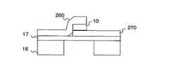
図10は歪検知素子装置200の好ましい位置を示す。歪検知素子装置200は基板15上に設けられた一つの歪検知素子10を用いる。基板15はSiO2/Si基板からMEMS技術を用いて作成されたSiメンブレンである。かかる設計では、基板15は平面図において円形である。しかしながら、製造を考慮して四角形又は長方形を用いることができる。FIG. 10 shows a preferred position of the strain
歪検知素子10は電極260及び電極270の間に設けられている。電極270は基板15に設けられている。電極260は歪検知素子10に設けられている。基板15が、ドープされたポリ3,4−エチレンヂオキシチオフェン、ポリスチレンサルフォネートのようなフレキシブルな導電性メンブレンであれば、電極270は直接歪検知素子10に接続されていなくても良い。配線の数を減らせばよりフレキシブルなメンブレンを作ることができる。The
歪検知素子10は基板15の中心に設けられている。基板15の中心は等方的な歪みが最も大きい。等方的な歪みの応答に対して歪検知素子装置200は歪検知素子10を利用できる。The
図11Aは基板15内の電極の構造を示す。基板15は、硬い基板16とメンブレン17からなる。メンブレン17は硬い基板16に固定されている。導電性メンブレン240はメンブレン17に設けられている。この導電性メンブレン240はコーティング層150に付随して用いられる。又は、導電性コーティング層が用いられても良い。歪検知素子10は導電性メンブレン240に設けられている。歪検知素子10は絶縁層250に囲まれている。歪検知素子10の上部は電極260に接続されている。FIG. 11A shows the structure of the electrodes in the
電極260の膜厚は、良好な電気的接続を保証するために、少なくとも100nmである。しかし、良質の積層がなされればより薄い電極260を用いることも可能である。The film thickness of the
絶縁層250はSiO2又はSi3N4の材料からなる。絶縁層250はポリメチルメタクリレートのような有機材料又は絶縁ドープされたポリ3、4エチレンジオキシチオフェン、ポリスチレンサルフォネートを用いることもできる。The insulating
電極260は導電メンブレンとして用いることができる。このようにすることでメンブレン17をより柔らかくし、歪みを均一にすることができる。しかし、歪検知素子10と電気的に接続することがより複雑になるかもしれない。The
図11B及び図11Cは歪検知素子10の動作を示す。実線の矢印は磁化自由層40の磁化の向きを示す。破線の矢印は参照層20の磁化の向きを示す(ここの層は示されていない)。11B and 11C show the operation of the
図11B及び図11Cは、メンブレン17に設けられた基板に歪みが適用されるときの状態を示す。この状態では、磁化自由層40の磁化は磁化自由層と参照層との間の垂直角の構成の変化を受けるために、歪みは磁化自由層40の磁化の回転を引き起こす。FIG. 11B and FIG. 11C show a state when strain is applied to the substrate provided on the
なぜなら、基板内に歪みが生じていないときに基板16はフレキシブルでないからである。メンブレン17はフレキシブルである。これは、基板が結合されていない自由な状態の領域で歪みが生じているためである。メンブレンの形状が規定されれば、印加される歪みに対して受ける歪みは一定である。歪検知素子10は歪みが起こる最も有利な位置のメンブレンに設けられる。This is because the
図11Bは歪みが小さい場合を示す。図11Cは歪みが大きい場合を示す。これらの図が示すように、歪みがより大きくなれば磁化自由層40の磁化受ける回転の大きさは大きくなる。FIG. 11B shows a case where the distortion is small. FIG. 11C shows a case where the distortion is large. As shown in these figures, when the strain becomes larger, the magnitude of the rotation that the magnetization
歪検知素子10に歪みが適用されれば、磁化自由層40の磁化は歪みの方向に沿って回転する。この回転は参照層20と磁化自由層40の磁化との間の角度を作る。歪検知素子10が歪みを受けていないときには、磁化自由層40の磁化の向きはもとに戻る。When strain is applied to the
図12は基板16内の電極の構造を示す。歪検知素子10は電極270と電極260との間に設けられている。電極260は電極270と交わらないで、メンブレン17に対して歪検知素子10の上部に設けられている。FIG. 12 shows the structure of the electrodes in the
外部からの影響を絶縁するためにさらに誘電層が電極上に設けられても良い。In order to insulate external influences, a dielectric layer may be further provided on the electrode.
図13は基板15上の複数の歪検知素子10を用いた歪検知素子装置200を示す。FIG. 13 shows a strain
歪検知素子10は、正方形のパターンとして基板15に設けられ、電気的にホイートストーンブリッジ配列を形成している。歪検知素子10にかかる電圧は典型的なホイートストーンブリッジの動作として正方形の中央で端末から読み出される。複数の歪検知素子10は基板15に設けられているので、ほかの測定ブリッジ回路を用いても良い。The
図14は、基板15に設けられた複数の歪検知素子10を用いる歪検知素子装置200を示す。FIG. 14 shows a strain
歪検知素子10は連続して接続されている。これは信号の強度と多くのセンサから得られるデータの平均出力を向上させるためである。この構造はい補正の歪みの方向に関係なく基板15の様々な場所で動作する歪検知素子10に利用できる。よって多くの歪検知素子10を用いることができる。個々に接続している歪検知素子10のように、機能に依存して他の代わりとなる回路配列も用いることができる。ゆえに、制御部とは別にアクセスすることができ、制御部の結果を処理することができ、他の接続された出力システムの処理をすることができる。
(第3の実施形態)The
(Third embodiment)
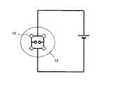
図15は歪検知素子10に応用される機器300を示す。FIG. 15 shows a
機器300は血圧センサを示す。図15の上図は血液が拡張していない動脈の状態を示す。図15の下図は血圧によって動脈が拡張している状態を示す。
機器300は腕又は体に巻きつけられる。腕又は体の表面近傍には動脈があり心拍数を測定するのに用いられる。
心臓が鼓動をうつとき、動脈は血液と一緒に拡張する。これは脈として知られている。動脈からの圧力が基板に適用されると歪みを引き起こす。この歪みは基板15に設けられた歪検知素子10によって検知される。そして磁気抵抗の変化の結果は歪検知素子10を測定する制御部で電気的に記録される。動脈の拡張が示す電気的な信号と周波数の発生はコンピュータで測定されたデータから変換される。これにより心拍数と血圧を決定することができる。As the heart beats, the arteries dilate with the blood. This is known as a pulse. When pressure from the artery is applied to the substrate, it causes distortion. This strain is detected by the
図16は歪検知素子10に応用される機器400を示す。FIG. 16 shows a
機器400は切り替え装置である。図16の上図はボタンが押されていない状態を示す。図16の下図はボタンが押されている状態を示す。The
機器400は、リモートコントロールのような一般的な切替えである。ボタン410はメンブレン17を固定している硬い基板16に設けられている。The
ボタン410が押されるとメンブレン17に対して圧力が加わり、歪みによりメンブレン17が歪む。係る場合、歪検知素子10はメンブレン17の下に設けられている。この位置に設けることでボタンを押すことによる衝撃を減らすことができる。この位置もまた、歪検知素子が圧縮歪みよりも引っ張り歪みを受けていることを保証している。When the
本発明のいくつかの実施形態を説明したが、これらの実施形態は、例として提示したものであり、発明の範囲を限定することは意図していない。これら新規な実施形態は、その他の様々な形態で実施されることが可能であり、発明の要旨を逸脱しない範囲で、種々の省略、置き換え、変更を行うことができる。これら実施形態やその変形は、発明の範囲や要旨に含まれるとともに、特許請求の範囲に記載された発明とその均等の範囲に含まれる。Although several embodiments of the present invention have been described, these embodiments are presented by way of example and are not intended to limit the scope of the invention. These novel embodiments can be implemented in various other forms, and various omissions, replacements, and changes can be made without departing from the scope of the invention. These embodiments and modifications thereof are included in the scope and gist of the invention, and are included in the invention described in the claims and the equivalents thereof.
10 … 歪検知素子、15 … 基板、20 … 参照層、30 … スペーサー層、40 … 磁化自由層、50 … 磁気抵抗素子、70 … 下地層DESCRIPTION OF
本発明の実施形態は、歪検知素子、および血圧センサに関する。Embodiments described herein relate generally to a strain sensing elementand a blood pressure sensor .
本発明の一態様に係る歪検知素子は、磁化方向が変化可能で、外部歪が印加されていない
状態では膜面垂直の磁化方向を有する磁化自由層と、磁化を有する参照層と、前記磁化自
由層と前記参照層との間に設けられたスペーサー層と、を備えた積層膜と、前記積層膜の
積層面に対して垂直方向に通電する一対の電極と、前記一対の電極の何れか一方に設けら
れた基板と、前記基板が歪むと、前記磁化自由層の磁化の回転角度と前記参照層の磁化の
回転角度が異なることを特徴とする。A strain sensing element according to one embodiment of the present invention includes a magnetization free layer having a magnetization direction perpendicular to a film surface in a state in which a magnetization direction can be changed and no external strain is applied, a reference layer having magnetization, and the magnetization A laminatedfilm provided with a spacer layer provided between a free layer and the reference layer, a pair of electrodes that are energized in a direction perpendicular to a laminated surface of the laminatedfilm , and any one of the pair of electrodes When the substrate provided on one side and the substrate are distorted, the magnetization rotation angle of the magnetization free layer and the magnetization rotation angle of the reference layer are different.
図1Aと図1Bは、歪検知素子10を示す。歪検知素子10は、基板15の上に、参照層
20と、スペーサー層30と、磁化自由層40とを備えたスピンバルブ膜構造が形成され
ている。参照層20、および磁化自由層40は磁性材料で形成される。スペーサー層30
は、基本的には非磁性材料からなる。しかし、後述するように、磁性材料もスペーサーと
して機能するものに関して用いることができる。スピンバルブ膜に電流を流すために、一
対の電極が用いられる。CIP(Current−in−plane)配置では、図1A
のように一対の電極501、502が用いられる。CPP(Current−perpe
ndicular−to−plane)配置では、図1Bのように一対の電極511、5
12が用いられる。スピンバルブ膜から基板への電流を絶縁する目的や、基板表面の荒れ
を緩和するために、コーティング層150がCIP配置とCPP配置の両方に用いられる
。参照層20/スペーサー層30/磁化自由層40の積層膜の下地として、下地層70を
用いる。以下、それぞれの部分について詳細に説明する。積層膜は参照層20、スペーサ
ー層30、及び磁化自由層40で定義される。1A and 1B show a
Is basically made of a non-magnetic material. However, as will be described later, magnetic materials can also be used for those that function as spacers. A pair of electrodes is used to pass a current through the spin valve film. In the CIP (Current-in-plane) arrangement, FIG.
Thus, a pair of
In the (ndicular-to-plane) arrangement, a pair of
12 is used. In order to insulate the current from the spin valve film to the substrate and to reduce the roughness of the substrate surface, the
スペーサー層30は、MR現象の物理的な効果に依存して、数種類のバリエーションを有
している。MR現象としてTMR効果を用いる場合、MgOような材料が、典型的な材料
として用いられる。Al、Ti、Zn、Si、Hf、Ta、Mo、Wo、Nb、Cr、M
g、又はZrに基づく酸化物、窒化物、または酸窒化物も用いることができる。MR現象
としてGMR効果を用いる場合、CIP配置でもCPP配置でもスペーサー層30は、C
u、Au、Ag、Au、又はCrのような金属材料を用いることができる。このような単
純金属層だけでなく、CPP配置の場合には、電流狭窄(CCP: Current−C
onfined−Path)スペーサーを用いることもできる。CCPスペーサーには、
絶縁層を上下に貫通する複数のナノオーダーのメタルパスが用いられる。CCPスペーサ
ーを用いることの利点は、MR効果を高めるだけでなく、抵抗の大きさも制御することが
可能なことである。CCPスペーサーのメタルパス材料としては、単純金属スペーサーの
材料群と同じCu、Au、Ag、Al、又はCrなどであり、絶縁層はAl、Ti、Zn
、Si、Hf、Ta、Mo、Wo、Nb、Cr、Mg、又はZrに基づく酸化物、窒化物
、又は酸窒化物からなる。The
Oxides, nitrides, or oxynitrides based on g or Zr can also be used. When the GMR effect is used as the MR phenomenon, the
A metal material such as u, Au, Ag, Au, or Cr can be used. In the case of not only such a simple metal layer but also a CPP arrangement, current confinement (CCP: Current-C
on-path) spacers can also be used. For the CCP spacer,
A plurality of nano-order metal paths thatvertically penetrate the insulating layer are used. The advantage of using a CCP spacer is that not only the MR effect can be enhanced, but also the resistance can be controlled. The metal path material of the CCP spacer is Cu, Au, Ag, Al, or Cr, which is the same as the material group of the simple metal spacer, and the insulating layer is Al, Ti, Zn.
, Si, Hf, Ta, Mo, Wo, Nb, Cr, Mg, or an oxide, nitride, or oxynitride based on Zr.
上記2つのMRAM,STOに対し、本発明のように歪みセンサ・圧力検知素子に垂直異
方性を用いることの効果は全く異なる。前述したように、メンブレン内の歪検知素子が受
ける実際の歪みは、配置位置によっても異なり、非常に複雑である。圧縮応力か引っ張り
応力かという、極性の違いさえ、メンブレンの位置に依存して生じうる。このような状態
では、面内磁化を有する磁化自由層では抵抗の変化として検知できない場合もあり、検知
に関するSNR(Signal to Noise Ratio)劣化を引き起こす原因
になる。一方、膜面垂直磁化を有する磁化自由層40の場合、図1C、図1Dに示すよう
に抵抗変化を検知することができる。つまり、理想的な測定環境のみでしか測定できなか
ったのに対し、測定環境に対して高感度でロバストな、歪検知素子、圧力検知素子を実現
することができる。つまり、引っ張り応力、圧縮応力いずれの場合においても、膜面垂直
方向の磁化を有する磁化自由層を用いれば、歪を検知可能となる。これは、膜面内に磁化
を有する磁化自由層を用いている場合には実現できない。また、この効果は、MRAM、
STOにおいて膜面垂直方向の磁化を有する磁性層を用いる理由とは全く異なる。The effect of using vertical anisotropy for the strain sensor and pressure sensing element as in the present invention is completely different from the above two MRAM and STO. As described above, the actual strain received by the strain sensing element in the membrane varies depending on the arrangement position and is very complicated. Even a polarity difference, whether compressive or tensile, can occur depending on the position of the membrane. In such a state, the magnetization free layer having in-plane magnetization may not be detected as a change in resistance, which causes SNR (Signal to Noise Ratio) degradation related to detection. On the other hand, in the case of the magnetization
This is completely different from the reason for using a magnetic layer having magnetization in the direction perpendicular to the film surface in STO.
また、別の理由として、膜面垂直の磁気異方性を有する材料の場合、面内磁化を有する軟
磁性材料とは異なり、磁気異方性の大きさは大きい。その理由は、大きな磁気異方性を有
しないと、膜面内に磁化が向くことが有利な、形状異方性に打ち勝つことができないため
である。このような大きな磁気異方性をもつ磁性層を用いるということは、(1)式にお
けるHkが大きい材料を用いるということを意味する。つまり、外部歪が印加されていな
い状態において大きなHkをもつ磁化自由層のHkを外部歪によって変化させて検知する
には、ΔHkの値として、充分大きな変化量を発生させないと、変化量として検知できな
いことになる。つまり、ΔHkを通常の膜面内に磁化を有する磁化自由層を用いる場合よ
りもさらに大きなΔHkを発生させる必要がでてくる。すなわち、(1)式からわかるよ
うに、より大きなλの磁化自由層を用いることが必須となる。小さな磁歪定数λが求めら
れる従来の応用と比較すると、歪検知素子として用いる本発明の場合には、少なくとも磁
歪定数の絶対値が10−6よりも大きなλは必須となる。より好ましくは、磁化自由層の
磁歪定数の絶対値は10−5よりも大きな値を有することが必要とされる。As another reason, in the case of a material having magnetic anisotropy perpendicular to the film surface, the magnitude of magnetic anisotropy is large, unlike a soft magnetic material having in-plane magnetization. The reason is that without a large magnetic anisotropy, it is not possible to overcome the shape anisotropy, which is advantageous in that the magnetization is oriented in the film plane. Using a magnetic layer having such a large magnetic anisotropy means using a material having a large Hk in the equation (1). In other words, in order to detect the change of the Hk of the magnetization free layer having a large Hk by the external strain when no external strain is applied, the change is detected as a change amount unless a sufficiently large change amount is generated as the value of ΔHk. It will not be possible. That is, it is necessary to generate a larger ΔHk than when a magnetization free layer having magnetization in the normal film plane is used. That is, as can be seen from the equation (1), it is essential to use a larger magnetization free layer of λ. Compared to small magnetostriction constant λGaMotomu Me is conventional applications, in the case of the present invention for use as strain sensing element is a large λ than the absolute value of 10-6 at least magnetostriction constant required. More preferably, the absolute value of the magnetostriction constant of the magnetization free layer needs to have a value larger than 10−5 .
スピンバルブ膜の成膜の順序としては、参照層20/スペーサー層30/磁化自由層40
(参照層が下側に存在しているので「ボトムタイプ」と呼ばれる)又は磁化自由層40/
スペーサー層30/参照層20(参照層が上側に存在しているので「トップタイプ」と呼
ばれる)のどちらでも用いることができる。図1A,図1Bにおいてはボトム型における
実施例を示しているが、本発明の本質的な効果としては、ボトム型でもトップ型でも違い
は発生せず、同等である。The spin valve film is formed in the order of
(Referred to as “bottom type” because the reference layer is present underneath) or the magnetization
Either the
参照層20/スペーサー層30/磁化自由層40のボトム型又は磁化自由層40/スペー
サー層30/参照層20のトップ型のいずれの場合でも下地層70が用いられる。本明細
書において「下地層」という言葉は、広い概念を含んで用いる。「下地層」はバッファ層
、シード層、又はピニング層(図示せず)のような多層からなる。いくつかのこれらの層
は特有の膜構造に依存して省略されていてもよい。バッファ層は、フレキシブル基板から
生じる荒れのような予期せぬ効果を避けるために用いられる。コーティング層150でバ
ッファ効果が充分な場合は、下地層におけるバッファ層は省略できる。シード層は、参照
層20/スペーサー層30/磁化自由層40又は磁化自由層40/スペーサー層30/参
照層20の結晶配向性を制御するために用いられる。ピニング層は必要であれば参照層の
磁化を固定するために用いられる。In either case of the bottom type of the
磁性層Mpの材料選択はCoPt−SiO2グラニュラ、FePt、CoPt、CoPt
、(Co/Pd)多層膜、(Co/Pt)多層膜、又は(Co/Ir)多層膜を用いるこ
とができる。既に述べた、TbFe及び(Co/Ni)多層膜もMpの機能を有する材料
群という位置づけである。多層膜は、2層から10層程度積層したものである。The material selection of the magnetic layer Mp is CoPt—SiO2 granular, FePt, CoPt, CoPt
, (Co / Pd) multilayer film, (Co / Pt) multilayer film, or (Co / Ir) multilayer film can be used. The TbFe and (Co / Ni) multilayer films that have already been described also have the function of Mp.
It is positioned as agroup . The multilayer film is formed by laminating about 2 to 10 layers.
位置(b)の場合、基板15に歪みが適用されると、磁化自由層40の磁化は歪みの方向
に回転する。それゆえに、磁気抵抗の変化が検知できる。一方で、位置(a)、(c)の
場合では、磁化自由層の磁化は回転しない。なぜなら、磁化自由層40の磁化の向きは既
に歪みの方向に向いているからである。つまり、外部歪が印加されたことによる抵抗の変
化は生じないため、外部歪を全く検知できていないことになる。これはセンサ全体として
みたときに、検知できる箇所が限られているということになり、SNRとして非常に望ま
しくない。In the case of the position (b ), when strain is applied to the
歪検知素子10は連続して接続されている。これは信号の強度と多くのセンサから得られ
るデータの平均出力を向上させるためである。この構造は異方性の歪みの方向に関係なく
基板15の様々な場所で動作する歪検知素子10に利用できる。よって多くの歪検知素子
10を用いることができる。個々に接続している歪検知素子10のように、機能に依存し
て他の代わりとなる回路配列も用いることができる。ゆえに、制御部とは別にアクセスす
ることができ、制御部の結果を処理することができ、他の接続された出力システムの処理
をすることができる。The
Claims (11)
Translated fromJapanese磁化を有する参照層と、
前記磁化自由層と前記参照層との間に設けられたスペーサー層と、
を備えた積層体と、
前記積層体の膜面垂直方向に通電する一対の電極と、
前記一対の電極の何れか一方に設けられた基板と、
前記基板が歪むと、前記磁化自由層の磁化の回転角度と前記参照層の磁化の回転角度が異なることを特徴とする歪検知素子または圧力検知素子。A magnetization free layer in which the magnetization direction can be changed and the magnetization direction is perpendicular to the film surface when no external strain is applied;
A reference layer having magnetization;
A spacer layer provided between the magnetization free layer and the reference layer;
A laminate comprising:
A pair of electrodes energized in a direction perpendicular to the film surface of the laminate;
A substrate provided on any one of the pair of electrodes;
A strain sensing element or a pressure sensing element, wherein when the substrate is distorted, the rotation angle of magnetization of the magnetization free layer is different from the rotation angle of magnetization of the reference layer.
磁化を有する参照層と、
前記磁化自由層と前記参照層との間に設けられたスペーサー層と、
を備えた積層体と、
前記積層体の膜面積層面に対して平行方向に通電する一対の電極と、
前記一対の電極の何れか一方に設けられた基板と、
前記基板が歪むと、前記磁化自由層の磁化の回転角度と前記参照層の磁化の回転角度が異なることを特徴とする歪検知素子または圧力検知素子。A magnetization free layer in which the magnetization direction can be changed and the magnetization direction is perpendicular to the film surface when no external strain is applied;
A reference layer having magnetization;
A spacer layer provided between the magnetization free layer and the reference layer;
A laminate comprising:
A pair of electrodes energized in a direction parallel to the film area layer surface of the laminate;
A substrate provided on any one of the pair of electrodes;
A strain sensing element or a pressure sensing element, wherein when the substrate is distorted, the rotation angle of magnetization of the magnetization free layer is different from the rotation angle of magnetization of the reference layer.
請求項4に記載の歪検知素子または圧力検知素子。In addition to the magnetic layer Mp and the magnetic layer Ml, a CoFeB layer or a CoFe layer is provided as a magnetization free layer at the spacer layer interface.
The strain sensing element or pressure sensing element according to claim 4.
Priority Applications (6)
| Application Number | Priority Date | Filing Date | Title |
|---|---|---|---|
| JP2010223175AJP5235964B2 (en) | 2010-09-30 | 2010-09-30 | Strain sensing element, strain sensing element device, and blood pressure sensor |
| US13/110,392US8760154B2 (en) | 2010-09-30 | 2011-05-18 | Strain sensor element and blood pressure sensor |
| US14/219,878US9066661B2 (en) | 2010-09-30 | 2014-03-19 | Strain sensor element and blood pressure sensor |
| US14/219,860US9131856B2 (en) | 2010-09-30 | 2014-03-19 | Strain sensor element and blood pressure sensor |
| US14/813,783US9999356B2 (en) | 2010-09-30 | 2015-07-30 | Strain sensor element and blood pressure sensor |
| US15/974,030US10342439B2 (en) | 2010-09-30 | 2018-05-08 | Strain sensor element and blood pressure sensor |
Applications Claiming Priority (1)
| Application Number | Priority Date | Filing Date | Title |
|---|---|---|---|
| JP2010223175AJP5235964B2 (en) | 2010-09-30 | 2010-09-30 | Strain sensing element, strain sensing element device, and blood pressure sensor |
Publications (2)
| Publication Number | Publication Date |
|---|---|
| JP2012078186Atrue JP2012078186A (en) | 2012-04-19 |
| JP5235964B2 JP5235964B2 (en) | 2013-07-10 |
Family
ID=45888658
Family Applications (1)
| Application Number | Title | Priority Date | Filing Date |
|---|---|---|---|
| JP2010223175AExpired - Fee RelatedJP5235964B2 (en) | 2010-09-30 | 2010-09-30 | Strain sensing element, strain sensing element device, and blood pressure sensor |
Country Status (2)
| Country | Link |
|---|---|
| US (5) | US8760154B2 (en) |
| JP (1) | JP5235964B2 (en) |
Cited By (30)
| Publication number | Priority date | Publication date | Assignee | Title |
|---|---|---|---|---|
| JP2014052360A (en)* | 2012-09-10 | 2014-03-20 | Toshiba Corp | Pressure detection element and manufacturing method thereof |
| JP2014103539A (en)* | 2012-11-20 | 2014-06-05 | Toshiba Corp | Microphone package |
| WO2015033464A1 (en)* | 2013-09-09 | 2015-03-12 | 株式会社日立製作所 | Magnetic sensor element |
| JP2015061057A (en)* | 2013-09-20 | 2015-03-30 | 株式会社東芝 | Strain detection element, pressure sensor, microphone, blood pressure sensor, and touch panel |
| JP2015061059A (en)* | 2013-09-20 | 2015-03-30 | 株式会社東芝 | Strain detection element, pressure sensor, microphone, blood pressure sensor, and touch panel |
| JP2015059925A (en)* | 2013-09-20 | 2015-03-30 | 株式会社東芝 | Inertial sensor |
| JP2015061056A (en)* | 2013-09-20 | 2015-03-30 | 株式会社東芝 | Strain sensing element, pressure sensor, microphone, blood pressure sensor, and touch panel |
| JP2015061070A (en)* | 2013-09-20 | 2015-03-30 | 株式会社東芝 | Strain detection element, pressure sensor, microphone, blood pressure sensor, and touch panel |
| JP2015059932A (en)* | 2013-09-20 | 2015-03-30 | 株式会社東芝 | Distortion detection element, pressure sensor, microphone, blood pressure sensor, and touch panel |
| JP2016015412A (en)* | 2014-07-02 | 2016-01-28 | 株式会社東芝 | Strain detection element, pressure sensor, microphone, blood pressure sensor, and touch panel |
| JP2016014581A (en)* | 2014-07-02 | 2016-01-28 | 株式会社東芝 | Pressure sensor, microphone using pressure sensor, blood pressure sensor and touch panel |
| US9322726B2 (en) | 2014-01-20 | 2016-04-26 | Kabushiki Kaisha Toshiba | Pressure sensor, acceleration sensor, and method for manufacturing pressure sensor |
| JP2016148687A (en)* | 2016-05-27 | 2016-08-18 | 株式会社東芝 | Element package and electric circuit |
| JP2016161410A (en)* | 2015-03-02 | 2016-09-05 | 株式会社東芝 | Strain detecting element, pressure sensor and microphone |
| JP2016212124A (en)* | 2016-09-23 | 2016-12-15 | 株式会社東芝 | Pressure sensor, acoustic microphone, blood pressure sensor and touch panel |
| US9581571B2 (en) | 2013-09-20 | 2017-02-28 | Kabushiki Kaisha Toshiba | Acoustic sensor and acoustic sensor system |
| JP2017045978A (en)* | 2015-08-28 | 2017-03-02 | 株式会社東芝 | Sensor and electronic equipment |
| JP2017138321A (en)* | 2017-03-15 | 2017-08-10 | 株式会社東芝 | Pressure sensor, acoustic microphone, blood pressure sensor, and touch panel |
| JP2017191112A (en)* | 2017-07-26 | 2017-10-19 | 株式会社東芝 | Inertial sensor |
| JP2017216461A (en)* | 2017-07-04 | 2017-12-07 | 株式会社東芝 | Strain sensing element, sensor, microphone, blood pressure sensor, and touch panel |
| JP2017220671A (en)* | 2017-07-04 | 2017-12-14 | 株式会社東芝 | Strain sensing element, pressure sensor, microphone, blood pressure sensor, and touch panel |
| US9853209B2 (en) | 2014-03-19 | 2017-12-26 | Kabushiki Kaisha Toshiba | Method of manufacturing pressure sensor, deposition system, and annealing system |
| US9952030B2 (en) | 2015-03-24 | 2018-04-24 | Kabushiki Kaisha Toshiba | Strain sensing element and pressure sensor |
| JP2018087827A (en)* | 2018-02-28 | 2018-06-07 | 株式会社東芝 | Pressure sensor, microphone, blood pressure sensor, and touch panel |
| JP2018100975A (en)* | 2018-02-07 | 2018-06-28 | 株式会社東芝 | Pressure sensor, acoustic microphone, blood pressure sensor and touch panel |
| JP2018105868A (en)* | 2018-01-09 | 2018-07-05 | 株式会社東芝 | Element package and electric circuit |
| JP2018201023A (en)* | 2018-07-10 | 2018-12-20 | 株式会社東芝 | Sensor, microphone, blood pressure sensor, and touch panel |
| US10234343B2 (en) | 2013-06-12 | 2019-03-19 | Kabushiki Kaisha Toshiba | Pressure sensor, acoustic microphone, blood pressure sensor, and touch panel |
| WO2023106130A1 (en)* | 2021-12-07 | 2023-06-15 | 国立大学法人大阪大学 | Distortion measurement device and distortion measurement method |
| WO2023153361A1 (en)* | 2022-02-09 | 2023-08-17 | 国立大学法人大阪大学 | Stress sensor |
Families Citing this family (39)
| Publication number | Priority date | Publication date | Assignee | Title |
|---|---|---|---|---|
| JP5235964B2 (en)* | 2010-09-30 | 2013-07-10 | 株式会社東芝 | Strain sensing element, strain sensing element device, and blood pressure sensor |
| JP5443421B2 (en) | 2011-03-24 | 2014-03-19 | 株式会社東芝 | Magnetoresistive element, magnetic head gimbal assembly, and magnetic recording / reproducing apparatus |
| JP5740268B2 (en) | 2011-09-27 | 2015-06-24 | 株式会社東芝 | Display device |
| JP5677258B2 (en) | 2011-09-27 | 2015-02-25 | 株式会社東芝 | Strain detector and method of manufacturing the same |
| JP5982795B2 (en) | 2011-11-30 | 2016-08-31 | ソニー株式会社 | Memory element and memory device |
| JP5579218B2 (en) | 2012-03-28 | 2014-08-27 | 株式会社東芝 | Manufacturing method of pressure sensing element |
| JP5701807B2 (en) | 2012-03-29 | 2015-04-15 | 株式会社東芝 | Pressure sensor and microphone |
| JP2014074606A (en) | 2012-10-03 | 2014-04-24 | Toshiba Corp | Pressure sensor, acoustic microphone, blood pressure sensor and touch panel |
| JP6055286B2 (en) | 2012-11-20 | 2016-12-27 | 株式会社東芝 | Pressure sensor, microphone, blood pressure sensor, and touch panel |
| JP6263356B2 (en)* | 2013-09-09 | 2018-01-17 | 株式会社東芝 | Strain detector and method of manufacturing the same |
| JP6074344B2 (en) | 2013-09-20 | 2017-02-01 | 株式会社東芝 | Pressure sensor, microphone, blood pressure sensor, and touch panel |
| JP2015179779A (en)* | 2014-03-19 | 2015-10-08 | 株式会社東芝 | Strain detection element, pressure sensor, microphone, blood pressure sensor, and touch panel |
| JP6200358B2 (en)* | 2014-03-20 | 2017-09-20 | 株式会社東芝 | Pressure sensor, microphone, blood pressure sensor, and touch panel |
| JP6356583B2 (en)* | 2014-11-26 | 2018-07-11 | 東洋ゴム工業株式会社 | Sealed secondary battery monitoring sensor, sealed secondary battery, and sealed secondary battery monitoring method |
| US9647204B2 (en) | 2014-12-05 | 2017-05-09 | International Business Machines Corporation | Spin torque MRAM based on Co, Ir synthetic antiferromagnetic multilayer |
| US9263665B1 (en)* | 2014-12-10 | 2016-02-16 | Globalfoundries Singapore Pte. Ltd. | Two-bits per cell structure with spin torque transfer magnetic random access memory and methods for fabricating the same |
| JP6824504B2 (en)* | 2015-03-06 | 2021-02-03 | 株式会社BlueSpin | Magnetic memory, data writing method to magnetic memory and semiconductor device |
| JP2016194964A (en) | 2015-04-01 | 2016-11-17 | 株式会社BlueSpin | Magnetic memory and operation method thereof |
| JP6480837B2 (en)* | 2015-09-04 | 2019-03-13 | 株式会社東芝 | Sensor, information terminal, microphone, blood pressure sensor, and touch panel |
| JP6421101B2 (en)* | 2015-09-09 | 2018-11-07 | 株式会社東芝 | Sensor, information terminal, microphone, blood pressure sensor, and touch panel |
| US9966901B2 (en)* | 2015-11-19 | 2018-05-08 | Samsung Electronics Co., Ltd. | Spin-torque oscillator based on easy-cone anisotropy |
| US10361361B2 (en) | 2016-04-08 | 2019-07-23 | International Business Machines Corporation | Thin reference layer for STT MRAM |
| US9799823B1 (en) | 2016-04-08 | 2017-10-24 | International Business Machines Corporation | High temperature endurable MTJ stack |
| JP6631376B2 (en) | 2016-04-15 | 2020-01-15 | オムロンヘルスケア株式会社 | Pulse wave detecting device, biological information measuring device, control method of pulse wave detecting device, and control program of pulse wave detecting device |
| US11000193B2 (en)* | 2017-01-04 | 2021-05-11 | Livemetric (Medical) S.A. | Blood pressure measurement system using force resistive sensor array |
| JP6363271B2 (en)* | 2017-07-04 | 2018-07-25 | 株式会社東芝 | Sensor |
| US10746611B2 (en)* | 2017-12-07 | 2020-08-18 | Texas Instruments Incorporated | Magnetostrictive strain gauge sensor |
| US11166676B2 (en)* | 2017-12-11 | 2021-11-09 | Marina I. Adrianzen Fonseca | Real-time kidney monitoring medical device |
| US10845212B1 (en)* | 2018-01-11 | 2020-11-24 | Facebook Technologies, Llc | Giant magnetoresistance strain gauge sensor |
| JP6889135B2 (en)* | 2018-09-14 | 2021-06-18 | 株式会社東芝 | Sensor |
| JP6615971B2 (en)* | 2018-10-05 | 2019-12-04 | 株式会社東芝 | Sensor, microphone, blood pressure sensor, and touch panel |
| US10942072B2 (en) | 2018-11-20 | 2021-03-09 | International Business Machines Corporation | Nanoscale magnetic tunnel junction arrays for sub-micrometer resolution pressure sensor |
| CN111493817B (en)* | 2019-01-31 | 2023-10-10 | 周冠谦 | Stretchable flexible sensing device |
| CN110307778B (en)* | 2019-07-02 | 2020-03-06 | 清华大学 | Flexible signal sensing and processing device |
| CN111063796B (en)* | 2019-11-22 | 2021-10-15 | 西安交通大学 | A spin valve structural unit, device and control method for local strain control |
| CN111524715B (en)* | 2020-04-29 | 2021-04-06 | 华中科技大学 | Working electrode and electrochemical pressure sensor based on thin-film nested structure |
| JP2022144398A (en) | 2021-03-19 | 2022-10-03 | キオクシア株式会社 | Magnetic storage device |
| CN115200751A (en)* | 2022-06-29 | 2022-10-18 | 江苏多维科技有限公司 | Tactile sensor based on tunnel magnetoresistance effect |
| CN115581442A (en)* | 2022-08-26 | 2023-01-10 | 中国科学院空天信息创新研究院 | Blood pressure monitoring device, blood pressure monitoring bracelet and wearable blood pressure monitoring clothes |
Citations (5)
| Publication number | Priority date | Publication date | Assignee | Title |
|---|---|---|---|---|
| JP2002357489A (en)* | 2001-05-31 | 2002-12-13 | Matsushita Electric Ind Co Ltd | Stress sensor |
| JP2002357488A (en)* | 2001-05-31 | 2002-12-13 | Matsushita Electric Ind Co Ltd | Stress sensor |
| JP2003294545A (en)* | 2002-02-15 | 2003-10-15 | Sony Electronics Singapore Pte Ltd | Force detection device |
| JP2008107323A (en)* | 2006-10-24 | 2008-05-08 | Headway Technologies Inc | Magnetic film sensor and method of manufacturing the same |
| JP2009194393A (en)* | 2009-04-27 | 2009-08-27 | Toshiba Corp | Method for manufacturing magnetoresistive element |
Family Cites Families (18)
| Publication number | Priority date | Publication date | Assignee | Title |
|---|---|---|---|---|
| US5168760A (en)* | 1991-11-01 | 1992-12-08 | The United States Of America As Represented By The Secretary Of The Navy | Magnetic multilayer strain gage |
| WO1995028649A1 (en)* | 1994-04-15 | 1995-10-26 | Philips Electronics N.V. | A magnetic field sensor, an instrument comprising such a sensor and a method of manufacturing such a sensor |
| US5585986A (en)* | 1995-05-15 | 1996-12-17 | International Business Machines Corporation | Digital magnetoresistive sensor based on the giant magnetoresistance effect |
| US6694822B1 (en)* | 1999-07-20 | 2004-02-24 | Fidelica Microsystems, Inc. | Use of multi-layer thin films as stress sensor |
| JP4355439B2 (en) | 2000-11-09 | 2009-11-04 | 東北リコー株式会社 | Micro pressure sensing element, device using this element, and health monitoring system |
| DE10214946B4 (en)* | 2002-04-04 | 2006-01-19 | "Stiftung Caesar" (Center Of Advanced European Studies And Research) | TMR sensor |
| DE10319319A1 (en)* | 2003-04-29 | 2005-01-27 | Infineon Technologies Ag | Sensor device with magnetostrictive force sensor |
| US7800868B2 (en)* | 2005-12-16 | 2010-09-21 | Seagate Technology Llc | Magnetic sensing device including a sense enhancing layer |
| US7732881B2 (en)* | 2006-11-01 | 2010-06-08 | Avalanche Technology, Inc. | Current-confined effect of magnetic nano-current-channel (NCC) for magnetic random access memory (MRAM) |
| JP5235964B2 (en)* | 2010-09-30 | 2013-07-10 | 株式会社東芝 | Strain sensing element, strain sensing element device, and blood pressure sensor |
| JP5443421B2 (en) | 2011-03-24 | 2014-03-19 | 株式会社東芝 | Magnetoresistive element, magnetic head gimbal assembly, and magnetic recording / reproducing apparatus |
| JP5677258B2 (en) | 2011-09-27 | 2015-02-25 | 株式会社東芝 | Strain detector and method of manufacturing the same |
| JP5740268B2 (en) | 2011-09-27 | 2015-06-24 | 株式会社東芝 | Display device |
| JP5579218B2 (en) | 2012-03-28 | 2014-08-27 | 株式会社東芝 | Manufacturing method of pressure sensing element |
| JP5701807B2 (en) | 2012-03-29 | 2015-04-15 | 株式会社東芝 | Pressure sensor and microphone |
| JP2014074606A (en) | 2012-10-03 | 2014-04-24 | Toshiba Corp | Pressure sensor, acoustic microphone, blood pressure sensor and touch panel |
| JP5951454B2 (en) | 2012-11-20 | 2016-07-13 | 株式会社東芝 | Microphone package |
| JP6055286B2 (en) | 2012-11-20 | 2016-12-27 | 株式会社東芝 | Pressure sensor, microphone, blood pressure sensor, and touch panel |
- 2010
- 2010-09-30JPJP2010223175Apatent/JP5235964B2/ennot_activeExpired - Fee Related
- 2011
- 2011-05-18USUS13/110,392patent/US8760154B2/enactiveActive
- 2014
- 2014-03-19USUS14/219,878patent/US9066661B2/enactiveActive
- 2014-03-19USUS14/219,860patent/US9131856B2/enactiveActive
- 2015
- 2015-07-30USUS14/813,783patent/US9999356B2/enactiveActive
- 2018
- 2018-05-08USUS15/974,030patent/US10342439B2/enactiveActive
Patent Citations (5)
| Publication number | Priority date | Publication date | Assignee | Title |
|---|---|---|---|---|
| JP2002357489A (en)* | 2001-05-31 | 2002-12-13 | Matsushita Electric Ind Co Ltd | Stress sensor |
| JP2002357488A (en)* | 2001-05-31 | 2002-12-13 | Matsushita Electric Ind Co Ltd | Stress sensor |
| JP2003294545A (en)* | 2002-02-15 | 2003-10-15 | Sony Electronics Singapore Pte Ltd | Force detection device |
| JP2008107323A (en)* | 2006-10-24 | 2008-05-08 | Headway Technologies Inc | Magnetic film sensor and method of manufacturing the same |
| JP2009194393A (en)* | 2009-04-27 | 2009-08-27 | Toshiba Corp | Method for manufacturing magnetoresistive element |
Cited By (48)
| Publication number | Priority date | Publication date | Assignee | Title |
|---|---|---|---|---|
| JP2014052360A (en)* | 2012-09-10 | 2014-03-20 | Toshiba Corp | Pressure detection element and manufacturing method thereof |
| US9618411B2 (en) | 2012-09-10 | 2017-04-11 | Kabushiki Kaisha Toshiba | Pressure sensor device |
| JP2014103539A (en)* | 2012-11-20 | 2014-06-05 | Toshiba Corp | Microphone package |
| US10477323B2 (en) | 2012-11-20 | 2019-11-12 | Kabushiki Kaisha Toshiba | Microphone package |
| US10070230B2 (en) | 2012-11-20 | 2018-09-04 | Kabushiki Kaisha Toshiba | Microphone package |
| US10234343B2 (en) | 2013-06-12 | 2019-03-19 | Kabushiki Kaisha Toshiba | Pressure sensor, acoustic microphone, blood pressure sensor, and touch panel |
| JPWO2015033464A1 (en)* | 2013-09-09 | 2017-03-02 | 株式会社日立製作所 | Magnetic sensor element |
| WO2015033464A1 (en)* | 2013-09-09 | 2015-03-12 | 株式会社日立製作所 | Magnetic sensor element |
| US9810711B2 (en) | 2013-09-20 | 2017-11-07 | Kabushiki Kaisha Toshiba | Inertial sensor |
| US10254305B2 (en) | 2013-09-20 | 2019-04-09 | Kabushiki Kaisha Toshiba | Inertial sensor |
| JP2015061057A (en)* | 2013-09-20 | 2015-03-30 | 株式会社東芝 | Strain detection element, pressure sensor, microphone, blood pressure sensor, and touch panel |
| US9897494B2 (en) | 2013-09-20 | 2018-02-20 | Kabushiki Kaisha Toshiba | Strain sensing element, pressure sensor, microphone, blood pressure sensor, and touch panel |
| US9342179B2 (en) | 2013-09-20 | 2016-05-17 | Kabushiki Kaisha Toshiba | Strain sensing element, pressure sensor, microphone, blood pressure sensor, and touch panel |
| US10448845B2 (en) | 2013-09-20 | 2019-10-22 | Kabushiki Kaisha Toshiba | Strain sensing element, having a first and second magnetic layer and a third layer that is antiferrimagnetic |
| US10444085B2 (en) | 2013-09-20 | 2019-10-15 | Kabushiki Kaisha Toshiba | Strain sensing element, pressure sensor, microphone, blood pressure sensor, and touch panel |
| US10413198B2 (en) | 2013-09-20 | 2019-09-17 | Kabushiki Kaisha Toshiba | Strain sensing element, pressure sensor, microphone, blood pressure sensor, and touch panel |
| US9581571B2 (en) | 2013-09-20 | 2017-02-28 | Kabushiki Kaisha Toshiba | Acoustic sensor and acoustic sensor system |
| US9872624B2 (en) | 2013-09-20 | 2018-01-23 | Kabushiki Kaisha Toshiba | Strain sensing element, pressure sensor, microphone, blood pressure sensor, and touch panel |
| JP2015059932A (en)* | 2013-09-20 | 2015-03-30 | 株式会社東芝 | Distortion detection element, pressure sensor, microphone, blood pressure sensor, and touch panel |
| JP2015061070A (en)* | 2013-09-20 | 2015-03-30 | 株式会社東芝 | Strain detection element, pressure sensor, microphone, blood pressure sensor, and touch panel |
| US9654883B2 (en) | 2013-09-20 | 2017-05-16 | Kabushiki Kaisha Toshiba | Strain sensing element, pressure sensor, microphone, blood pressure sensor, and touch panel |
| US9651432B2 (en) | 2013-09-20 | 2017-05-16 | Kabushiki Kaisha Toshiba | Strain sensing element, pressure sensor, microphone, blood pressure sensor, and touch panel |
| JP2015061059A (en)* | 2013-09-20 | 2015-03-30 | 株式会社東芝 | Strain detection element, pressure sensor, microphone, blood pressure sensor, and touch panel |
| US10190923B2 (en) | 2013-09-20 | 2019-01-29 | Kabushiki Kaisha Toshiba | Strain sensing element, pressure sensor, microphone, blood pressure sensor, and touch panel |
| JP2015061056A (en)* | 2013-09-20 | 2015-03-30 | 株式会社東芝 | Strain sensing element, pressure sensor, microphone, blood pressure sensor, and touch panel |
| JP2015059925A (en)* | 2013-09-20 | 2015-03-30 | 株式会社東芝 | Inertial sensor |
| US9322726B2 (en) | 2014-01-20 | 2016-04-26 | Kabushiki Kaisha Toshiba | Pressure sensor, acceleration sensor, and method for manufacturing pressure sensor |
| US9853209B2 (en) | 2014-03-19 | 2017-12-26 | Kabushiki Kaisha Toshiba | Method of manufacturing pressure sensor, deposition system, and annealing system |
| JP2016014581A (en)* | 2014-07-02 | 2016-01-28 | 株式会社東芝 | Pressure sensor, microphone using pressure sensor, blood pressure sensor and touch panel |
| JP2016015412A (en)* | 2014-07-02 | 2016-01-28 | 株式会社東芝 | Strain detection element, pressure sensor, microphone, blood pressure sensor, and touch panel |
| US10082435B2 (en) | 2014-07-02 | 2018-09-25 | Kabushiki Kaisha Toshiba | Pressure sensor |
| US10048150B2 (en) | 2014-07-02 | 2018-08-14 | Kabushiki Kaisha Toshiba | Strain detection element, pressure sensor, microphone, blood pressure sensor, and touch panel |
| JP2016161410A (en)* | 2015-03-02 | 2016-09-05 | 株式会社東芝 | Strain detecting element, pressure sensor and microphone |
| US10746526B2 (en) | 2015-03-24 | 2020-08-18 | Kabushiki Kaisha Toshiba | Strain sensing element and pressure sensor |
| US9952030B2 (en) | 2015-03-24 | 2018-04-24 | Kabushiki Kaisha Toshiba | Strain sensing element and pressure sensor |
| JP2017045978A (en)* | 2015-08-28 | 2017-03-02 | 株式会社東芝 | Sensor and electronic equipment |
| JP2016148687A (en)* | 2016-05-27 | 2016-08-18 | 株式会社東芝 | Element package and electric circuit |
| JP2016212124A (en)* | 2016-09-23 | 2016-12-15 | 株式会社東芝 | Pressure sensor, acoustic microphone, blood pressure sensor and touch panel |
| JP2017138321A (en)* | 2017-03-15 | 2017-08-10 | 株式会社東芝 | Pressure sensor, acoustic microphone, blood pressure sensor, and touch panel |
| JP2017216461A (en)* | 2017-07-04 | 2017-12-07 | 株式会社東芝 | Strain sensing element, sensor, microphone, blood pressure sensor, and touch panel |
| JP2017220671A (en)* | 2017-07-04 | 2017-12-14 | 株式会社東芝 | Strain sensing element, pressure sensor, microphone, blood pressure sensor, and touch panel |
| JP2017191112A (en)* | 2017-07-26 | 2017-10-19 | 株式会社東芝 | Inertial sensor |
| JP2018105868A (en)* | 2018-01-09 | 2018-07-05 | 株式会社東芝 | Element package and electric circuit |
| JP2018100975A (en)* | 2018-02-07 | 2018-06-28 | 株式会社東芝 | Pressure sensor, acoustic microphone, blood pressure sensor and touch panel |
| JP2018087827A (en)* | 2018-02-28 | 2018-06-07 | 株式会社東芝 | Pressure sensor, microphone, blood pressure sensor, and touch panel |
| JP2018201023A (en)* | 2018-07-10 | 2018-12-20 | 株式会社東芝 | Sensor, microphone, blood pressure sensor, and touch panel |
| WO2023106130A1 (en)* | 2021-12-07 | 2023-06-15 | 国立大学法人大阪大学 | Distortion measurement device and distortion measurement method |
| WO2023153361A1 (en)* | 2022-02-09 | 2023-08-17 | 国立大学法人大阪大学 | Stress sensor |
Also Published As
| Publication number | Publication date |
|---|---|
| US9066661B2 (en) | 2015-06-30 |
| US10342439B2 (en) | 2019-07-09 |
| US20140207007A1 (en) | 2014-07-24 |
| US9131856B2 (en) | 2015-09-15 |
| US20140207006A1 (en) | 2014-07-24 |
| JP5235964B2 (en) | 2013-07-10 |
| US20120079887A1 (en) | 2012-04-05 |
| US20180256035A1 (en) | 2018-09-13 |
| US9999356B2 (en) | 2018-06-19 |
| US8760154B2 (en) | 2014-06-24 |
| US20150338292A1 (en) | 2015-11-26 |
Similar Documents
| Publication | Publication Date | Title |
|---|---|---|
| JP5235964B2 (en) | Strain sensing element, strain sensing element device, and blood pressure sensor | |
| JP4433820B2 (en) | Magnetic detection element, method of forming the same, magnetic sensor, and ammeter | |
| Grünberg | Layered magnetic structures: History, highlights, applications | |
| JP6212000B2 (en) | Pressure sensor, and microphone, blood pressure sensor, and touch panel using pressure sensor | |
| JP5951454B2 (en) | Microphone package | |
| US10746526B2 (en) | Strain sensing element and pressure sensor | |
| US7532504B2 (en) | Spin injection magnetic domain wall displacement device and element thereof | |
| US9618411B2 (en) | Pressure sensor device | |
| JP6211866B2 (en) | Pressure sensor, microphone, blood pressure sensor, and touch panel | |
| US20060238191A1 (en) | Spin injection magnetic domain wall displacement device and element thereof | |
| JP4692805B2 (en) | Magnetic sensing element and method for forming the same | |
| CN101000943A (en) | Magnetic sensing device including sensing enhancement layer | |
| CN101958123A (en) | Magnetic Sensor with perpendicular magnetic anisotropy free layer and side direction shield member | |
| JP2005019990A (en) | Magnetic device with improved antiferromagnetic coupling film | |
| CN101252037A (en) | Magnetic film and magnetoresistance effect element | |
| JP6491367B2 (en) | Device package and electric circuit | |
| JP2005018973A (en) | Magnetic recording disk with improved antiferromagnetic coupling film | |
| JP6317783B2 (en) | Device package and electric circuit | |
| JP2008210905A (en) | Tunnel magnetoresistive element | |
| JPWO2008102786A1 (en) | Magnetic detector | |
| JP2010213115A (en) | Magneto-coupling type isolator | |
| JPH11283830A (en) | Magnetoresistance effect film | |
| JP2000011334A (en) | Magneto-resistance effect element and magneto- resistance effect type magnetic head |
Legal Events
| Date | Code | Title | Description |
|---|---|---|---|
| A977 | Report on retrieval | Free format text:JAPANESE INTERMEDIATE CODE: A971007 Effective date:20120927 | |
| A131 | Notification of reasons for refusal | Free format text:JAPANESE INTERMEDIATE CODE: A131 Effective date:20121002 | |
| A521 | Request for written amendment filed | Free format text:JAPANESE INTERMEDIATE CODE: A523 Effective date:20121203 | |
| A131 | Notification of reasons for refusal | Free format text:JAPANESE INTERMEDIATE CODE: A131 Effective date:20121221 | |
| A521 | Request for written amendment filed | Free format text:JAPANESE INTERMEDIATE CODE: A523 Effective date:20130111 | |
| TRDD | Decision of grant or rejection written | ||
| A01 | Written decision to grant a patent or to grant a registration (utility model) | Free format text:JAPANESE INTERMEDIATE CODE: A01 Effective date:20130301 | |
| A61 | First payment of annual fees (during grant procedure) | Free format text:JAPANESE INTERMEDIATE CODE: A61 Effective date:20130326 | |
| R151 | Written notification of patent or utility model registration | Ref document number:5235964 Country of ref document:JP Free format text:JAPANESE INTERMEDIATE CODE: R151 | |
| FPAY | Renewal fee payment (event date is renewal date of database) | Free format text:PAYMENT UNTIL: 20160405 Year of fee payment:3 | |
| LAPS | Cancellation because of no payment of annual fees |