JP2012069224A - Nonvolatile semiconductor memory - Google Patents
Nonvolatile semiconductor memoryDownload PDFInfo
- Publication number
- JP2012069224A JP2012069224AJP2010214243AJP2010214243AJP2012069224AJP 2012069224 AJP2012069224 AJP 2012069224AJP 2010214243 AJP2010214243 AJP 2010214243AJP 2010214243 AJP2010214243 AJP 2010214243AJP 2012069224 AJP2012069224 AJP 2012069224A
- Authority
- JP
- Japan
- Prior art keywords
- memory
- memory cell
- write
- threshold voltage
- memory cells
- Prior art date
- Legal status (The legal status is an assumption and is not a legal conclusion. Google has not performed a legal analysis and makes no representation as to the accuracy of the status listed.)
- Pending
Links
Images


Landscapes
- Read Only Memory (AREA)
- Semiconductor Memories (AREA)
- Non-Volatile Memory (AREA)
Abstract
Translated fromJapaneseDescription
Translated fromJapanese本実施形態は、不揮発性半導体記憶装置に関する。 The present embodiment relates to a nonvolatile semiconductor memory device.
従来、シリコン基板上の2次元平面内に素子を集積して、LSIが形成されてきた。メモリの記憶容量を増加させるには、一素子の寸法を小さくする(微細化する)のが一般的だが、近年その微細化もコスト的、技術的に困難なものになってきた。微細化のためにはフォトリソグラフィの技術向上が必要であるが、リソグラフィ工程に要するコストは増加の一途を辿っている。また、仮に微細化が達成されたとしても、駆動電圧などがスケーリングされない限り、素子間の耐圧など物理的な限界点を迎える事が予想される。つまり、デバイスとしての動作が困難になる可能性が高い。 Conventionally, LSIs have been formed by integrating elements in a two-dimensional plane on a silicon substrate. In order to increase the storage capacity of a memory, it is common to reduce the size of one element (miniaturize), but in recent years, the miniaturization has become costly and technically difficult. For miniaturization, photolithography technology needs to be improved, but the cost required for the lithography process is steadily increasing. Even if miniaturization is achieved, it is expected that physical limits such as breakdown voltage between elements will be reached unless the drive voltage is scaled. That is, there is a high possibility that operation as a device is difficult.
そこで、近年、メモリの集積度を高めるために、メモリセルを3次元的に配置した不揮発性半導体記憶装置(積層型の不揮発性半導体記憶装置)が多数提案されている。 Therefore, in recent years, many nonvolatile semiconductor memory devices (stacked nonvolatile semiconductor memory devices) in which memory cells are three-dimensionally arranged have been proposed in order to increase the degree of memory integration.
本実施形態は、データリテンションの特性を向上しつつ消去動作や書き込み動作に要する時間を短縮できる不揮発性半導体記憶装置を提供する。 The present embodiment provides a nonvolatile semiconductor memory device that can shorten the time required for the erase operation and the write operation while improving the characteristics of data retention.
以下に説明する実施の形態の不揮発性半導体記憶装置は、第1書き込み領域と第2書き込み領域を有し、複数のメモリセルを含むメモリセルアレイを備える。制御回路は、複数のメモリセルに対して印加する電圧を制御する。制御回路は、複数のメモリセルに対し消去動作を実行する場合に、第2書き込み領域のメモリセルに隣接する第1書き込み領域のメモリセルを除いた第1書き込み領域のメモリセルに第1閾値電圧を与える一方、第2書き込み領域のメモリセル及び第2書き込み領域のメモリセルに隣接する第1書き込み領域のメモリセルに第1閾値電圧より電圧値が大きい消去状態を示す正の第2閾値電圧を与えるよう制御する。 A nonvolatile semiconductor memory device according to an embodiment described below includes a memory cell array having a first write area and a second write area and including a plurality of memory cells. The control circuit controls the voltage applied to the plurality of memory cells. When performing an erase operation on a plurality of memory cells, the control circuit applies a first threshold voltage to the memory cells in the first write region excluding the memory cells in the first write region adjacent to the memory cells in the second write region. On the other hand, a positive second threshold voltage indicating an erase state having a voltage value larger than the first threshold voltage is applied to the memory cell in the second write area and the memory cell in the first write area adjacent to the memory cell in the second write area. Control to give.
以下、図面を参照して、本発明に係る不揮発性半導体記憶装置の実施形態について説明する。 Hereinafter, embodiments of a nonvolatile semiconductor memory device according to the present invention will be described with reference to the drawings.
[第1の実施の形態]
[構成]
先ず、図1を参照して、第1実施形態に係る不揮発性半導体記憶装置の全体構成について説明する。図1は、本発明の第1実施形態に係る不揮発性半導体記憶装置のブロック図である。[First Embodiment]
[Constitution]
First, the overall configuration of the nonvolatile semiconductor memory device according to the first embodiment will be described with reference to FIG. FIG. 1 is a block diagram of a nonvolatile semiconductor memory device according to the first embodiment of the present invention.
第1実施形態に係る不揮発性半導体記憶装置は、図1に示すように、メモリセルアレイ11、ロウデコーダ12、データ回路・ページバッファ13、カラムデコーダ14、制御回路15、入出力回路16、アドレス・コマンドレジスタ17、内部電圧発生回路18、およびコアドライバ19を備える。 As shown in FIG. 1, the nonvolatile semiconductor memory device according to the first embodiment includes a
メモリセルアレイ11は、図2に示すように、カラム方向に延びた複数のビット線BLと、ビット線BLに交差するロウ方向に延びた複数のソース線CELSRCと、電気的に書き換え可能な複数のメモリセルMTrを直列に接続されたメモリストリングMSを有する。メモリセルアレイ11は、図2に示すように、データを電気的に記憶するメモリセルMTrを3次元マトリクス状に配列して構成される。すなわち、メモリセルMTrは、積層方向にマトリクス状に配列されるとともに、積層方向に直交する水平方向にも配列される。積層方向に並ぶ複数個のメモリセルMTrは直列接続され、メモリストリングMSを構成する。 As shown in FIG. 2, the
メモリストリングMSの両端には選択時に導通状態とされるドレイン側選択トランジスタSDTr、ソース側選択トランジスタSSTrが接続される。このメモリストリングMSは、積層方向を長手方向として配列される。ドレイン側選択トランジスタSDTrの一端は、ビット線BLに接続される。ソース側選択トランジスタSSTrの一端は、ソース線CELSRCに接続される。 A drain-side selection transistor SDTr and a source-side selection transistor SSTr that are conductive when selected are connected to both ends of the memory string MS. The memory strings MS are arranged with the stacking direction as a longitudinal direction. One end of the drain side select transistor SDTr is connected to the bit line BL. One end of the source side select transistor SSTr is connected to the source line CELSRC.
ロウデコーダ12は、図1に示すように、アドレス・コマンドレジスタ17から入力されたブロックアドレス信号等をデコードし、またコアドライバ19から出力されるワード線制御信号や選択ゲート制御信号を受けて、メモリセルアレイ11を制御する。データ回路・ページバッファ13は、読み出し動作時にはメモリセルアレイ11からデータを読み出し、ページバッファにデータを一時的に保持する。また、書き込み動作時にはチップ外部から書き込みデータがページバッファにロードされた後、ページバッファとデータ回路が連携して選択されたメモリセルにデータを書き込む。カラムデコーダ14は、アドレス・コマンドレジスタ17から入力されたカラムアドレス信号をデコードし、データの入出力制御を行う。制御回路15は、アドレス・コマンドレジスタ17から読み出し・書き込み・消去動作等を実行する信号を受けて、所定のシーケンスに従って、コア動作に必要な種々の電圧を発生する内部電圧発生回路18を制御したり、ワード線やビット線制御の制御を司るコアドライバ19を制御する。入出力回路16は、コマンド・アドレス・データの入出力制御を行う。この不揮発性半導体記憶装置には、高速書き込み領域と通常書き込み領域が設けられており、それぞれの領域で行われる消去動作は、互いに異なっている。詳しくは後述する。 As shown in FIG. 1, the
次に、図3を参照して、メモリセルアレイ11の回路構成について説明する。図3は、メモリセルアレイ11のカラム方向の断面に沿って形成されるメモリセルMTr、ドレイン側選択トランジスタSDTr、ソース側選択トランジスタSSTr、及びその周辺回路の等価回路図である。 Next, the circuit configuration of the
メモリセルアレイ11は、図3に示すように、複数のビット線BL、及び複数のメモリブロックMBを有する。ビット線BLは、ロウ方向に所定ピッチをもってカラム方向に複数のメモリブロックMBに跨るように延びるストライプ状に形成されている。メモリブロックMBは、所定ピッチをもってカラム方向に繰り返し設けられている。 As shown in FIG. 3, the
メモリブロックMBは、図3に示すように、ロウ方向及びロウ方向と直交するカラム方向にマトリクス状に配列された複数のメモリユニットMUを有する。メモリブロックMBにおいて、一本のビット線BLには、共通接続された複数のメモリユニットMUが設けられている。メモリユニットMUは、メモリストリングMS、ソース側選択トランジスタSSTr、及びドレイン側選択トランジスタSDTrを有する。カラム方向に隣接するメモリユニットMUは、その構成がカラム方向に互いに対称となるように形成されている。メモリユニットMUは、ロウ方向及びカラム方向にマトリクス状に配列されている。ロウ方向において一列に並ぶ複数のメモリユニットMUは、1つのサブブロックSBを構成する。 As shown in FIG. 3, the memory block MB has a plurality of memory units MU arranged in a matrix in the row direction and the column direction orthogonal to the row direction. In the memory block MB, one bit line BL is provided with a plurality of commonly connected memory units MU. The memory unit MU includes a memory string MS, a source side selection transistor SSTr, and a drain side selection transistor SDTr. The memory units MU adjacent to each other in the column direction are formed so that their configurations are symmetrical to each other in the column direction. The memory units MU are arranged in a matrix in the row direction and the column direction. A plurality of memory units MU arranged in a line in the row direction constitute one sub-block SB.
メモリストリングMSは、直列接続されたメモリセルMTr0〜MTr15、及びバックゲートトランジスタBTrにて構成されている。メモリセルMTr0〜MTr7は、積層方向に直列に接続されている。メモリセルMTr8〜MTr15も、同様に積層方向に直列に接続されている。メモリセルMTr0〜MTr15は、電荷蓄積層に電荷を蓄積させることで、情報を記憶する。 The memory string MS is composed of memory cells MTr0 to MTr15 and a back gate transistor BTr connected in series. The memory cells MTr0 to MTr7 are connected in series in the stacking direction. Similarly, the memory cells MTr8 to MTr15 are connected in series in the stacking direction. The memory cells MTr0 to MTr15 store information by storing charges in the charge storage layer.
バックゲートトランジスタBTrは、最下層のメモリセルMTr7とメモリセルMTr8との間に接続されている。従って、メモリセルMTr0〜MTr15、及びバックゲートトランジスタBTrは、カラム方向に沿った断面においてU字形状に接続されている。ソース側選択トランジスタSSTrのドレインは、メモリストリングMSの他端(メモリセルMTr0のソース)に接続されている。ドレイン側選択トランジスタSDTrのソースは、メモリストリングMSの一端(メモリセルMTr15のドレイン)に接続されている。 The back gate transistor BTr is connected between the lowermost memory cell MTr7 and the memory cell MTr8. Accordingly, the memory cells MTr0 to MTr15 and the back gate transistor BTr are connected in a U shape in a cross section along the column direction. The drain of the source side select transistor SSTr is connected to the other end of the memory string MS (the source of the memory cell MTr0). The source of the drain side select transistor SDTr is connected to one end of the memory string MS (the drain of the memory cell MTr15).
メモリユニットMUにおいて、1つのメモリブロックMB中のメモリセルMTr0のゲートは、ワード線WL0に共通接続されている。同様に、1つのメモリブロックMB中のメモリセルMTr1〜MTr15のゲートは、ワード線WL1〜WL15に共通接続されている。また、ロウ方向及びカラム方向にマトリクス状に配列されたバックゲートトランジスタBTrのゲートは、バックゲート線BGに共通接続されている。 In the memory unit MU, the gates of the memory cells MTr0 in one memory block MB are commonly connected to the word line WL0. Similarly, the gates of the memory cells MTr1-MTr15 in one memory block MB are commonly connected to the word lines WL1-WL15. Further, the gates of the back gate transistors BTr arranged in a matrix in the row direction and the column direction are commonly connected to the back gate line BG.
メモリユニットMUにおいて、ロウ方向に一列に配列された各ドレイン側選択トランジスタSDTrのゲートは、ロウ方向に延びるドレイン側選択ゲート線SGDに共通接続されている。また、カラム方向に一列に配列されたドレイン側選択トランジスタSDTrのドレインは、ビット線BLに共通に接続されている。 In the memory unit MU, the gates of the drain side select transistors SDTr arranged in a line in the row direction are commonly connected to a drain side select gate line SGD extending in the row direction. The drains of the drain side select transistors SDTr arranged in a line in the column direction are commonly connected to the bit line BL.
メモリユニットMUにおいて、ロウ方向に一列に配列された各ソース側選択トランジスタSSTrのゲートは、ロウ方向に延びるソース側選択ゲート線SGSに共通接続されている。また、カラム方向に隣接する一対のメモリユニットMUにおいて、ロウ方向に一列に配列されたソース側選択トランジスタSSTrのソースは、ロウ方向に延びるソース線CELSRCに共通に接続されている。 In the memory unit MU, the gates of the source side select transistors SSTr arranged in a line in the row direction are commonly connected to a source side select gate line SGS extending in the row direction. Further, in a pair of memory units MU adjacent in the column direction, the sources of the source side select transistors SSTr arranged in a line in the row direction are commonly connected to a source line CELSRC extending in the row direction.
次に、図4を参照して、図3に示した回路構成を実現するメモリセルアレイ11の積層構造について説明する。図4は、第1実施形態に係るメモリセルアレイ11の断面図であり、図5は、図4の一部の拡大図である。 Next, a stacked structure of the
メモリセルアレイ11は、図4に示すように、基板20、下層から順に、バックゲート層30、メモリセル層40、選択トランジスタ層50、及び配線層60を有する。バックゲート層30は、バックゲートトランジスタBTrとして機能する。メモリセル層40は、メモリセルMTr0〜MTr15として機能する。選択トランジスタ層50は、ドレイン側選択トランジスタSDTr、及びソース側選択トランジスタSSTrとして機能する。配線層60は、ソース線CELSRC及びビット線BLとして機能する。 As shown in FIG. 4, the
バックゲート層30は、図4に示すように、基板20の上に絶縁層21を介して形成されたバックゲート導電層31を有する。バックゲート導電層31は、バックゲート線BG、及びバックゲートトランジスタBTrのゲートとして機能する。バックゲート導電層31は、ロウ方向及びカラム方向に広がる板状に形成されている。バックゲート導電層31は、後述するU字状半導体層45の連結部45Bの下面及び側面を覆い且つ連結部45Bの上面と同じ高さまで形成されている。バックゲート導電層31は、ポリシリコン(poly−Si)にて構成されている。 As shown in FIG. 4, the
また、バックゲート層30は、図4に示すように、バックゲート導電層31を堀込むように形成されたバックゲート溝32を有する。バックゲート溝32は、ロウ方向に短手方向、カラム方向に長手方向を有する開口にて構成されている。バックゲート溝32は、ロウ方向及びカラム方向に所定間隔毎にマトリクス状に形成されている。 Further, as shown in FIG. 4, the
メモリセル層40は、図4に示すように、積層方向に絶縁層42を介して形成されたワード線導電層41a〜41dを有する。ワード線導電層41a〜41dは、ワード線WL0〜WL15、及びメモリセルMTr0〜MTr15の制御ゲートとして機能する。ワード線導電層41a〜41dは、メモリブロックMB毎に分断され、ロウ方向に対向する一対の櫛歯状に形成されている。あるいは、メモリユニットMU毎に、ワード線WLが独立に駆動になるよう、ワード線導電層41a〜41dも1つのメモリユニット毎に独立のコンタクトに接続されていてもよい。
ワード線導電層41a〜41dは、カラム方向に所定ピッチをもってロウ方向に延びるストライプ状に形成された部分を有する。ワード線導電層41a〜41dは、ポリシリコン(poly−Si)あるいはポリサイドにて構成されている。As shown in FIG. 4, the memory cell layer 40 includes word line
The word line
また、メモリセル層40は、図4に示すように、ワード線導電層41a〜41d、及び絶縁層42を貫通するように形成されたメモリホール43を有する。 Further, as shown in FIG. 4, the memory cell layer 40 has
メモリホール43は、各バックゲート溝32のカラム方向の両端近傍の位置に整合するように形成されている。メモリホール43は、ロウ方向及びカラム方向にマトリクス状に形成されている。 The
また、上記バックゲートトランジスタ層30及びメモリセル層40は、図4に示すように、メモリゲート絶縁層44、及びU字状半導体層45を有する。U字状半導体層45は、メモリセルMTr0〜MTr15及びバックゲートトランジスタBTrのボディとして機能する。 Further, the back
メモリゲート絶縁層44は、図4に示すように、メモリホール43、及びバックゲート溝32に面する側面に、メモリセル間においても分断されず、連続的に形成されている。メモリゲート絶縁層44は、図5に示すように、ブロック絶縁層44a、電荷蓄積層44b、及びトンネル絶縁層44cにて構成されている。ブロック絶縁層44aは、メモリホール43、及びバックゲート溝32に面する側面に亘ってワード線導電層41a〜41d及びバックゲート導電層31と接するように形成されている。ブロック絶縁層44aは、酸化シリコン(SiO2)にて構成されている。電荷蓄積層44bは、ブロック絶縁層44aの側面に形成されている。電荷絶縁層44bは、電荷を蓄積し、メモリセルMTr0〜MTr15のデータを保有するために用いられる。電荷蓄積層44bは、窒化シリコン(SiN)にて構成されている。トンネル絶縁層44cは、電荷蓄積層44bの側面に形成されている。トンネル絶縁層44cは、酸化シリコン(SiO2)にて構成されている。As shown in FIG. 4, the memory
U字状半導体層45は、図4に示すように、ロウ方向からみてU字状に形成されている。U字状半導体層45は、図5に示すように、トンネル絶縁層44cに接し且つバックゲート溝32及びメモリホール43を埋めるように形成されている。U字状半導体層45は、ロウ方向からみて基板20に対して垂直方向に延びる一対の柱状部45A、及び一対の柱状部45Aの下端を連結させるように形成された連結部45Bを有する。U字状半導体層45は、ポリシリコン(poly−Si)にて構成されている。 As shown in FIG. 4, the
上記メモリセル層40の構成を換言すると、トンネル絶縁層44cは、柱状部45Aの側面を取り囲むように形成されている。電荷蓄積層44bは、トンネル絶縁層44cの側面を取り囲むように形成されている。ブロック絶縁層44aは、電荷蓄積層44bの側面を取り囲むように形成されている。ワード線導電層41a〜41dは、ブロック絶縁層44aの側面を取り囲むように形成されている。なお、電荷蓄積層44bは、ワード線導電層41a〜41dの側面だけでなく、それらの間の層間絶縁膜の側面にも形成され、柱状部45aの側面に上下方向に連続的に形成されている。ブロック絶縁層44a、トンネル絶縁層44cも同様である。 In other words, in the configuration of the memory cell layer 40, the
選択トランジスタ層50は、図4に示すように、ドレイン側導電層51、及びそのドレイン側導電層51と同層に形成されたソース側導電層52を有する。ドレイン側導電層51は、ドレイン側選択ゲート線SGD、及びドレイン側選択トランジスタSDTrのゲート電極として機能する。ソース側導電層52は、ソース側選択ゲート線SGS、及びソース側選択トランジスタSSTrのゲート電極として機能する。 As shown in FIG. 4, the
ドレイン側導電層51、及びソース側導電層52は、カラム方向に所定ピッチをもってロウ方向に延びるストライプ状に形成されている。ドレイン側導電層51、及びソース側導電層52は、カラム方向に2つずつ交互に設けられている。ドレイン側導電層51、及びソース側導電層52は、ポリシリコン(poly−Si)にて構成されている。 The drain side
また、選択トランジスタ層50は、図4に示すように、ドレイン側ホール53、及びソース側ホール54を有する。ドレイン側ホール53は、ドレイン側導電層51を貫通するように形成されている。ソース側ホール54は、ソース側導電層52を貫通するように形成されている。ドレイン側ホール53及びソース側ホール54は、メモリホール43に整合する位置に形成されている。 Further, as shown in FIG. 4, the
また、選択トランジスタ層50は、図4に示すように、ドレイン側ゲート絶縁層55、ソース側ゲート絶縁層56、ドレイン側柱状半導体層57、及びソース側柱状半導体層58を有する。ドレイン側柱状半導体層57は、ドレイン側選択トランジスタSDTrのボディとして機能する。ソース側柱状半導体層58は、ソース側選択トランジスタSSTrのボディと機能する。 As shown in FIG. 4, the
ドレイン側ゲート絶縁層55は、ドレイン側ホール53に面する側面に形成されている。ソース側ゲート絶縁層56は、ソース側ホール54に面する側面に形成されている。ドレイン側ゲート絶縁層55及びソース側ゲート絶縁層56は、酸化シリコン(SiO2)にて構成されている。The drain side gate insulating layer 55 is formed on the side surface facing the
ドレイン側柱状半導体層57は、ドレイン側ホール53を埋めるように、ドレイン側ゲート絶縁層55と接して積層方向に延びる柱状に形成されている。ソース側柱状半導体層58は、ソース側ホール54を埋めるように、ソース側ゲート絶縁層56と接して積層方向に延びる柱状に形成されている。ドレイン側柱状半導体層57、及びソース側柱状半導体層58は、ポリシリコン(poly−Si)にて構成されている。 The drain side
上記選択トランジスタ層50の構成を換言すると、ドレイン側ゲート絶縁層55は、ドレイン側柱状半導体層57の側面を取り囲むように形成されている。ドレイン側導電層51は、ドレイン側ゲート絶縁層55の側面を取り囲むように形成されている。ソース側ゲート絶縁層56は、ソース側柱状半導体層58の側面を取り囲むように形成されている。ソース側導電層52は、ソース側ゲート絶縁層56の側面を取り囲むように形成されている。 In other words, the drain-side gate insulating layer 55 is formed so as to surround the side surface of the drain-side
配線層60は、図4に示すように、第1配線層61、第2配線層62、及びプラグ層63を有する。第1配線層61は、ソース線CELSRCとして機能する。第2配線層62は、ビット線BLとして機能する。 As shown in FIG. 4, the
第1配線層61は、図4に示すように、隣接する2本のソース側柱状半導体層58の上面に共通に接するように形成されている。第1配線層61は、カラム方向に所定ピッチをもってロウ方向に延びるストライプ状に形成されている。第1配線層61は、タングステン(W)等の金属にて構成されている。 As shown in FIG. 4, the
第2配線層62は、図4に示すように、プラグ層63を介してドレイン側柱状半導体層57の上面に接続されている。第2配線層62は、ロウ方向に所定ピッチをもってカラム方向に延びるストライプ状に形成されている。第2配線層62は、銅(Cu)、プラグ層63は、タングステン(W)等の金属にて構成されている。 As shown in FIG. 4, the
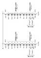
この不揮発性半導体記憶装置では、メモリセルアレイ11中において、通常書き込み領域と、高速書き込み領域とが定義されている。例えば図6に示すように、1メモリストリングMS中で、ワード線WL0およびWL1に沿ったメモリセルMC0およびMC1が高速書き込み領域(第1書込み領域)として定義され、ワード線WL2〜15に沿ったメモリセルMC2〜MC15が通常書き込み領域(第2書き込み領域)として定義される。 In this nonvolatile semiconductor memory device, a normal writing area and a high-speed writing area are defined in the
図7〜図9は、両書き込み領域における消去動作、書き込み動作の違いを説明する概念図である。書き込み動作完了後においては、データ”1”(消去状態)を示す閾値電圧分布E’又はデータ”0”を示す閾値電圧分布Aのいずれかが1つのメモリセルMCに与えられているものとする。閾値電圧分布E’は、消去動作により閾値電圧分布Eが得られた後、このような閾値電圧分布Eを有するメモリセルに対し弱い書き込み動作を行うことにより得られる分布である。すなわち、閾値電圧分布Eは、閾値電圧分布E’よりも低い分布である。
ここで、閾値電圧分布E’を与える必要性と、そのような閾値電圧分布E’を得るための制御方法について説明する。本実施の形態では、メモリセル構造の一例として、電荷蓄積層44bがメモリストリングMSの長手方向のメモリセルMC間でも分断されず繋がっているセルアレイ構造を挙げている。このようなセルアレイ構造において、あるメモリセルMTriが消去動作を受けた後閾値電圧分布Eに維持され、これによりメモリセルMTriの電荷蓄積層44bにホール(正孔)がトラップされている一方、それに隣接するメモリセルMTri+1が書き込み動作の対象とされ電荷蓄積層44bに電子がトラップされている場合を考える。この場合、メモリセルMTri+1の電荷蓄積層44bにトラップされている電子は、隣接するメモリセルMtriの電荷蓄積層44bにトラップされたホールの影響を受けてメモリセルMTri側に引き寄せられメモリセルMTri+1の電荷蓄積膜から抜け出し易くなる。その結果、書き込み状態にあったメモリセルMTri+1の閾値電圧が低下しやすくなりデータリテンション特性の悪化に繋がる。そこで、このような現象を緩和する一つの対策として、書き込み状態のメモリセルMTri+1に隣接するメモリセルMTri+1の電荷蓄積膜にホールが存在しないようにすることが有効であると考えられる。すなわち、データを書き込んだメモリセルMTri+1とメモリストリングMSの長手方向において隣接するメモリセルMTriには、その電荷蓄積層44bにホールが存在しない状態を保証する制御方法を採用する。ここで、メモリセルMTrで、1ビット/セル(2値記憶セル)の記憶方式を実行する場合には、メモリセルMTrは“1”と“0”の2状態のいずれかを保持する。また、2ビット/セル(4値記憶セル)の記憶方式を実行する場合には、メモリセルMTrは“11”/“10”/“00”/“01”の4状態のいずれかを保持する。いずれの記憶方式を実行する場合にも、複数の状態のうちのいずれか一つの状態、例えば最も低い閾値電圧分布を有する状態(例えば“1”状態または“11”状態)を消去状態に設定するが、その消去状態のメモリセルの閾値電圧分布は、隣接メモリセルのデータリテンションを悪化させないような所定レベルに設定される。そのように制御された消去状態の分布を、以下では閾値電圧分布E’と称する。
以下に通常書き込み領域、高速書き込み領域のそれぞれにおける書き込み動作、消去動作の制御方法を説明する。通常書き込み領域のメモリセルと高速書き込み領域のメモリセルとが同等のデータリテンション特性をもつように、通常書き込み領域又は高速書き込み領域に存在するメモリセルMTriにデータを書き終えた後には、メモリストリングMSの長手方向において隣接するメモリセルMTri+1には閾値電圧分布E’分布以上の閾値電圧分布が与えられるよう、メモリセルMTr+1の電圧印加が制御される。7 to 9 are conceptual diagrams illustrating the difference between the erase operation and the write operation in both write regions. After the write operation is completed, one of the threshold voltage distribution E ′ indicating data “1” (erased state) and the threshold voltage distribution A indicating data “0” is applied to one memory cell MC. . The threshold voltage distribution E ′ is a distribution obtained by performing a weak write operation on the memory cells having such a threshold voltage distribution E after the threshold voltage distribution E is obtained by the erase operation. That is, the threshold voltage distribution E is a distribution lower than the threshold voltage distribution E ′.
Here, the necessity to provide the threshold voltage distribution E ′ and a control method for obtaining such a threshold voltage distribution E ′ will be described. In the present embodiment, as an example of the memory cell structure, a cell array structure in which the charge storage layer 44b is connected without being divided between the memory cells MC in the longitudinal direction of the memory string MS is given. In such a cell array structure, after a certain memory cell MTri is subjected to an erasing operation, the threshold voltage distribution E is maintained, whereby holes are trapped in the charge storage layer 44b of the memory cell MTri. Consider a case where an adjacent memory cell MTri + 1 is a target of a write operation and electrons are trapped in the charge storage layer 44b. In this case, electrons trapped in the charge storage layer 44b of the memory cell MTri + 1 are attracted to the memory cell MTri side under the influence of the holes trapped in the charge storage layer 44b of the adjacent memory
Hereinafter, a method for controlling the writing operation and the erasing operation in the normal writing area and the high-speed writing area will be described. After data has been written to the memory cell MTri existing in the normal write area or the high-speed write area, the memory string MS is written so that the memory cell in the normal write area and the memory cell in the high-speed write area have equivalent data retention characteristics. The voltage application of the memory cell MTr + 1 is controlled so that the threshold voltage distribution equal to or higher than the threshold voltage distribution E ′ distribution is given to the memory cell MTri + 1 adjacent in the longitudinal direction of the.
この場合において、通常書き込み領域における消去動作では、閾値電圧分布A及びE’を有するメモリセルの閾値電圧を、閾値電圧分布E’以下の閾値電圧分布Eに移行させる(図7の動作(1))。この積層型不揮発性メモリの消去動作は、セルソースCELSRCに消去電圧Veraを印加し、ソース側選択ゲート線SGSのレベルを所定電圧に制御することによってSSTrのソース端でGIDL(Gate Induced Drain Current)を引き起こし、そこで発生したホールによって柱状半導体層58および57を充電してメモリセルのチャネル側を消去電圧Veraに高める一方、制御ゲートには電圧Veraよりも低い電圧(例えば接地電圧Vss)を印加することにより行う。ここで、消去動作の単位は、前述した複数のメモリセルユニットMUからなるブロックMBとなり、これらを基本的にはほぼ同一の消去電圧Veraと選択ワード線電圧の関係で、同時に消去する。後述の書き込み動作で行うようなビット毎制御による個々のメモリセルの精細な制御ができないため、消去後の閾値電圧分布Eの分布幅は個々のメモリセルのばらつきを反映した広い分布幅となり、閾値電圧分布Eを狭い分布とすることが難しい。この消去動作後の閾値電圧分布Eは、データ“1”に相当するものであるが、データ“1”の分布として完成していない状態の分布と考えることができる。 In this case, in the erase operation in the normal write region, the threshold voltage of the memory cell having the threshold voltage distributions A and E ′ is shifted to the threshold voltage distribution E equal to or lower than the threshold voltage distribution E ′ (operation (1) in FIG. 7). ). In this erase operation of the stacked nonvolatile memory, the erase voltage Vera is applied to the cell source CELSRC, and the level of the source-side selection gate line SGS is controlled to a predetermined voltage, so that the GDL (Gate Induced Drain Current) is generated at the source end of the SSTr. The columnar semiconductor layers 58 and 57 are charged by the generated holes to increase the channel side of the memory cell to the erase voltage Vera, while a voltage lower than the voltage Vera (for example, the ground voltage Vss) is applied to the control gate. By doing. Here, the unit of the erase operation is the block MB composed of the plurality of memory cell units MU described above, and these are erased at the same time basically based on the relationship between the almost identical erase voltage Vera and the selected word line voltage. Since fine control of individual memory cells by bit-by-bit control that is performed in a write operation described later cannot be performed, the distribution width of the threshold voltage distribution E after erasure becomes a wide distribution width that reflects the variation of the individual memory cells. It is difficult to make the voltage distribution E narrow. The threshold voltage distribution E after the erase operation corresponds to the data “1”, but can be considered as a distribution in a state where the distribution of the data “1” is not completed.
一方、高速書き込み領域における消去動作では、動作(1)に加え、メモリセルの閾値電圧分布が、消去動作後の閾値電圧分布Eから、所定の正の値をもった閾値電圧分布E’に変わるよう弱書き込み動作(図7の動作(2))を行う。この正の閾値電圧分布E’は、前述の消去動作後の閾値電圧分布Eから弱い書きこみ動作を行って、閾値電圧分布Eを正方向に移動させて得られる分布である。この閾値電圧分布E’には、メモリセルの消去状態(データ”1”)が割り当てられており、これが消去状態の閾値電圧分布の完成形となる。閾値電圧分布E’の書き込み時間は、書き込み方法や閾値電圧分布幅の割り当てに依存するが、図7に示すような2値の動作であれば、ページ毎に300μS程度かかる。したがって、(1)の消去動作自体に1.5msかかるとすると、消去時間の合計は、高速書き込み領域が2ページある場合には、2.4ms(=1.5ms+(2+1)*300us)、10ページある場合には、4.8ms(=1.5ms+(10+1)*300us)に達する。このように、消去動作に関しては、高速書き込み領域における消去時間は、通常書き込み領域における消去時間よりも長くなる。 On the other hand, in the erase operation in the high-speed write region, in addition to the operation (1), the threshold voltage distribution of the memory cell changes from the threshold voltage distribution E after the erase operation to a threshold voltage distribution E ′ having a predetermined positive value. The weak write operation (operation (2) in FIG. 7) is performed. The positive threshold voltage distribution E ′ is a distribution obtained by performing a weak write operation from the threshold voltage distribution E after the above-described erasing operation and moving the threshold voltage distribution E in the positive direction. The threshold voltage distribution E ′ is assigned with the erased state (data “1”) of the memory cell, which is a completed form of the threshold voltage distribution in the erased state. The writing time of the threshold voltage distribution E ′ depends on the writing method and the assignment of the threshold voltage distribution width, but it takes about 300 μS for each page in the binary operation as shown in FIG. Therefore, if the erase operation itself of (1) takes 1.5 ms, the total erase time is 2.4 ms (= 1.5 ms + (2 + 1) * 300 us) when there are two pages in the high-speed write area, 10 When there is a page, it reaches 4.8 ms (= 1.5 ms + (10 + 1) * 300 us). As described above, with respect to the erasing operation, the erasing time in the high-speed writing area is longer than the erasing time in the normal writing area.
通常書き込み領域における書き込み動作は、図8に示すような手順で行われる。書き込み動作の開始前においては、通常書き込み領域内(WL2〜15)のメモリセルの殆どは、閾値電圧分布Eを有している。この状態から、データ”1”を書き込みたいメモリセルには、閾値電圧分布EからE’に移行させる書き込み動作を実行する(図8の動作(3)))一方、データ”0”を書き込みたいメモリセルには、閾値電圧分布Eから閾値電圧分布Aに移行させる書き込み動作(図8の動作(4))を実行する。 The write operation in the normal write area is performed according to the procedure shown in FIG. Before the start of the write operation, most of the memory cells in the normal write region (WL2 to 15) have the threshold voltage distribution E. From this state, a memory cell to which data “1” is to be written is subjected to a write operation for shifting from the threshold voltage distribution E to E ′ (operation (3) in FIG. 8), while data “0” is to be written. A write operation (operation (4) in FIG. 8) for shifting from the threshold voltage distribution E to the threshold voltage distribution A is performed on the memory cell.
ここで、図8は、1本の選択ワード線WL上にある複数のメモリセルの書き込みについて着目した図になっている。このようなデータ書き込みがメモリストリングMSの長手方向に隣接する複数のメモリセルに対して連続して行われる場合には問題ない。しかし、1本のワード線のみの書き込みであったり、連続したページ書込みの最後のページへの書き込みである場合には、選択メモリセルに隣接するセルの閾値電圧が閾値電圧分布Eとなることがある。前述のように、閾値電圧分布Eを書き込まれたメモリセルと、書き込み動作後の閾値電圧分布A,B,Cを書き込まれたメモリセルとが隣接すると、データリテンション特性が悪化して信頼性上問題となる。したがって、上記の場合には、選択メモリセル自身の書き込みだけでなく、何らかの方法で、隣接メモリセルに閾値電圧分布E’を書き込む手段、制御があるものと仮定する。 Here, FIG. 8 is a diagram paying attention to writing of a plurality of memory cells on one selected word line WL. There is no problem when such data writing is continuously performed on a plurality of memory cells adjacent in the longitudinal direction of the memory string MS. However, in the case of writing to only one word line or writing to the last page of continuous page writing, the threshold voltage of the cell adjacent to the selected memory cell may become the threshold voltage distribution E. is there. As described above, if the memory cell in which the threshold voltage distribution E is written and the memory cell in which the threshold voltage distributions A, B, and C after the write operation are adjacent to each other, the data retention characteristic is deteriorated and reliability is increased. It becomes a problem. Therefore, in the above case, it is assumed that there is means and control for writing the threshold voltage distribution E ′ to the adjacent memory cell by some method, not just writing the selected memory cell itself.
一方、高速書き込み領域における書き込み動作は、図9に示すような手順で行われる。書き込み動作の開始前においては、高速書き込み領域内の全てのメモリセルは、閾値電圧分布Eよりも大きい閾値電圧分布E’を有している。この状態から、データ”1”を書き込みたいメモリセルでは、閾値電圧分布E’を維持するべく、書き込み禁止動作が行われる。一方、データ”0”を書き込みたいメモリセルには、閾値電圧分布E’から閾値電圧分布Aに移行させる書き込み動作が実行される。データ”1”を書き込みたいメモリセルにおいて書き込みのための電圧印加動作が不要であるため、書き込み動作の速度は、図8の場合より図9の場合の方が速くなる。つまり、高速書き込み領域における書き込み動作は、通常書き込み領域における書き込み動作に比べ、得るべき閾値電圧分布の数が少ないため(前者は1個、後者は2個)、書き込みスピードがおよそ2倍程度向上する。
なお、メモリストリングMSへの書き込み動作は、従来のNAND型フラッシュメモリと同様に、ソース線CELSRC側のメモリセルMC0を最初に書き込みセルとして選択し、以下順にビット線BLに近付く順に書き込みを実行するという順序で実行される。上記のように、1つのメモリセルに1ビットのデータを記憶する場合、1本のワード線WLi(i=0〜15)に沿った複数のメモリセルMCiに記憶されるデータは、1ページを構成する。これら1つのページには、1つのページデータが割り当てられる。本実施の形態では、図10に示すように、1本のメモリストリングMS中の高速書き込み領域に対応するワード線WL0に沿った複数のメモリセルMC0が、1つのページPAGE0を構成する。同様に、ワード線WL1に沿った複数のメモリセルMC1が、1つのページPAGE1を構成する。高速書き込み領域のみ選択して書き込みを行う場合には、図10に示すように、各メモリストリングMS内での書き込み順に従いページ選択をしつつ、その後適宜アドレス入力を行って別のメモリストリングを選択して、同様に高速書き込み領域のページ選択を行う。
なお、ワード線WL2の沿った複数のメモリセルMC2は、通常書き込み領域(WL2〜15)内に存在し且つ高速書き込み領域(WL0〜1)に隣接するメモリセルである。このメモリセルMC2は、他の通常書き込み領域内のメモリセルMC3〜15とは異なり(高速書き込み領域内のメモリセルMC0、MC1と同様に)、消去動作時において、消去動作後に閾値電圧分布Eから閾値電圧分布E’への弱書き込み動作の対象とされる。通常書き込み領域でありながら消去動作時において閾値電圧分布E’を書き込む必要がある理由は、以下の通りである。高速書き込み領域においては、書き込み時にどのワード線を選択した場合においても、その隣のワード線に沿ったメモリセルにおいて閾値電圧分布EからE’への書き込みが必要ないようにすることが求められる。そのような書き込みが必要になると、高速書き込み領域における書き込み速度が低下してしまうからである。前述のように、データ書き込みを行ったメモリセルの隣のメモリセルは、データリテンション特性の改善のため、閾値電圧分布EでなくE’を有している必要がある。しかし、高速書き込み領域の端部のメモリセルMCheに書き込みをする場合に、隣接する通常書き込み領域中のメモリセルMCneが閾値電圧分布Eを有していると、このため高速書き込み領域のメモリセルMCheへのデータ書き込みと共に、メモリセルMCneでの閾値電圧分布EからE’への弱書き込み動作も必要になってしまう。これでは、高速書き込み領域での書き込み速度が低下してしまう。このため、メモリセルMCneには、消去動作時において、閾値電圧分布EをE’に変える弱書き込み動作を実行している。On the other hand, the write operation in the high-speed write area is performed according to the procedure shown in FIG. Before the start of the write operation, all the memory cells in the high-speed write region have a threshold voltage distribution E ′ that is larger than the threshold voltage distribution E. From this state, in the memory cell to which data “1” is to be written, a write inhibit operation is performed in order to maintain the threshold voltage distribution E ′. On the other hand, a write operation for shifting from the threshold voltage distribution E ′ to the threshold voltage distribution A is performed on the memory cell to which data “0” is to be written. Since the voltage application operation for writing is not required in the memory cell to which data “1” is to be written, the speed of the writing operation is faster in the case of FIG. 9 than in the case of FIG. In other words, the write operation in the high-speed write region has a smaller number of threshold voltage distributions to be obtained than the write operation in the normal write region (one for the former and two for the latter), so the write speed is improved by about twice. .
In the write operation to the memory string MS, the memory cell MC0 on the source line CELSRC side is first selected as the write cell, and the write is executed in the order of approaching the bit line BL in the following order, as in the conventional NAND flash memory. It is executed in the order. As described above, when 1-bit data is stored in one memory cell, data stored in a plurality of memory cells MCi along one word line WLi (i = 0 to 15) Constitute. One page data is assigned to each one page. In the present embodiment, as shown in FIG. 10, a plurality of memory cells MC0 along the word line WL0 corresponding to the high-speed write region in one memory string MS constitute one page PAGE0. Similarly, a plurality of memory cells MC1 along the word line WL1 constitute one page PAGE1. When writing only the high-speed write area, as shown in FIG. 10, the page is selected according to the write order in each memory string MS, and then another address is input as appropriate to select another memory string. Similarly, the page selection of the high-speed writing area is performed.
The plurality of memory cells MC2 along the word line WL2 are memory cells that exist in the normal write region (WL2 to 15) and are adjacent to the high-speed write region (WL0 to 1). The memory cell MC2 is different from the memory cells MC3 to 15 in the other normal write regions (similar to the memory cells MC0 and MC1 in the high-speed write region), and from the threshold voltage distribution E after the erase operation in the erase operation. It is a target of weak write operation to the threshold voltage distribution E ′. The reason why it is necessary to write the threshold voltage distribution E ′ during the erase operation in the normal write area is as follows. In the high-speed writing region, it is required that no writing from the threshold voltage distribution E to E ′ is necessary in the memory cell along the adjacent word line, regardless of which word line is selected at the time of writing. This is because when such writing is necessary, the writing speed in the high-speed writing area is lowered. As described above, the memory cell adjacent to the memory cell to which data has been written needs to have E ′ instead of the threshold voltage distribution E in order to improve data retention characteristics. However, when writing to the memory cell MChe at the end of the high-speed write region, if the memory cell MCne in the adjacent normal write region has the threshold voltage distribution E, this causes the memory cell MChe in the high-speed write region. Along with the data write to the memory cell MCne, a weak write operation from the threshold voltage distribution E to E ′ in the memory cell MCne becomes necessary. This reduces the writing speed in the high-speed writing area. Therefore, a weak write operation for changing the threshold voltage distribution E to E ′ is performed on the memory cell MCne during the erase operation.
この高速書き込み領域のアドレス空間上の位置及び範囲は、この不揮発性記憶装置を利用するメモリーコントローラを含むメモリシステムの性能がもっとも向上するように設定される。よって、高速書き込み領域は、ブロックの中で、所定の1ページだけ(先頭ページ、最終ページ、あるいは所定のページ)でもよいし、所定ページ連続した領域(先頭ページから所定数、最終ページから所定数、あるいは所定ページから所定数)であってもよい。例えば、ブロックを消去する際に実際に消去動作を行わずに消去可能ブロックとしてフラグを書き込むメモリ制御方法がある。このように、データサイズは大きい必要はないが、所定のメモリアクセス情報を確実には速く書きこみたい場合に、上記先頭ページや最終ページに設定した小領域の高速書き込み領域が有効利用される。高速書き込み領域では、隣接セルの隣接セルも含めてあらかじめ閾値電圧分布E’が書き込まれているため、特にデータリテンション特性に関しては信頼性を満たし、かつ、書き込みが通常領域よりも速いメリットがある。
また、高速書き込み領域を所望のサイズにすることで、例えば、高いスループットで一時的にメモリセルアレイ内に書き込むデータバッファ領域として活用することができる。The position and range of the high-speed write area on the address space are set so that the performance of the memory system including the memory controller using the nonvolatile storage device is most improved. Therefore, the high-speed writing area may be only one predetermined page (first page, last page, or predetermined page) in a block, or a predetermined page continuous area (a predetermined number from the first page, a predetermined number from the last page). Or a predetermined number from a predetermined page). For example, there is a memory control method of writing a flag as an erasable block without actually performing an erasing operation when erasing the block. As described above, although the data size does not need to be large, the small area high-speed writing area set for the first page and the last page is effectively used when it is desired to write predetermined memory access information quickly and reliably. In the high-speed write area, the threshold voltage distribution E ′ is written in advance including the adjacent cells of the adjacent cells, so that there is an advantage that the reliability is satisfied particularly with respect to the data retention characteristic and the writing is faster than the normal area.
Further, by setting the high-speed writing area to a desired size, for example, it can be used as a data buffer area for temporarily writing into the memory cell array with high throughput.
図7〜図9では、1つのメモリセルに1ビット(2値)のデータが記憶される例を説明したが、1つのメモリセルに2ビット以上のデータを記憶させる場合にも、同様の動作が実行可能である。図11〜図13は、1つのメモリセルに2ビット(4値)のデータを記憶する場合における、通常書き込み領域と高速書き込み領域とにおける消去動作及び書き込み動作を概念的に示している。
書き込み動作完了後においては、閾値電圧分布E’、A,B,Cのいずれかが1つのメモリセルに与えられる。閾値電圧分布E’が2ビットデータ”11”(消去状態)に対応し、閾値電圧分布A,B,Cがそれぞれ例えばデータ”10”、”01”、”00”に対応している。7 to 9 illustrate an example in which 1-bit (binary) data is stored in one memory cell, the same operation is performed when data of 2 bits or more is stored in one memory cell. Is feasible. FIGS. 11 to 13 conceptually show an erase operation and a write operation in the normal write region and the high-speed write region in the case where 2-bit (four-valued) data is stored in one memory cell.
After the write operation is completed, one of the threshold voltage distributions E ′, A, B, and C is given to one memory cell. The threshold voltage distribution E ′ corresponds to 2-bit data “11” (erased state), and the threshold voltage distributions A, B, and C correspond to data “10”, “01”, and “00”, respectively.
この場合において、通常書き込み領域における消去動作では、図11に示すように、閾値電圧分布E’、A,B,またはCを有するメモリセルの閾値電圧を、閾値電圧分布E’以下の閾値電圧分布Eとなるまで消去動作を実行する(図11の動作(1))。一方、高速書き込み領域における消去動作では、動作(1)に加え、閾値電圧分布Eを所定の正の値を有する閾値電圧分布E’に移行させる弱書き込み動作(図11の動作(2))を行う。 In this case, in the erasing operation in the normal write region, as shown in FIG. 11, the threshold voltage distribution of the memory cell having the threshold voltage distribution E ′, A, B, or C is equal to or lower than the threshold voltage distribution E ′. The erase operation is executed until E is reached (operation (1) in FIG. 11). On the other hand, in the erase operation in the high-speed write region, in addition to the operation (1), a weak write operation (operation (2) in FIG. 11) for shifting the threshold voltage distribution E to the threshold voltage distribution E ′ having a predetermined positive value is performed. Do.
通常書き込み領域における書き込み動作は、図12に示すような手順で行われる。書き込み動作の開始前においては、通常書き込み領域内の全てのメモリトランジスタは、閾値電圧分布E’以下の閾値電圧分布Eを有している。この状態から、データ”11”を書き込みたいメモリセルには、閾値電圧分布EからE’に移行させる書き込み動作を実行する(図12の動作(3)))。一方、データ”10”、”01”、及び”00”を書き込みたいメモリセルには、閾値電圧分布Eから閾値電圧分布A,B,Cに移行させる書き込み動作(図12の動作(4))を実行する。 The write operation in the normal write area is performed according to the procedure shown in FIG. Before the start of the write operation, all the memory transistors in the normal write region have a threshold voltage distribution E that is equal to or lower than the threshold voltage distribution E ′. From this state, a write operation for shifting from the threshold voltage distribution E to E ′ is executed for the memory cell to which data “11” is to be written (operation (3) in FIG. 12)). On the other hand, for the memory cells to which data “10”, “01”, and “00” are to be written, a write operation for shifting from the threshold voltage distribution E to the threshold voltage distributions A, B, and C (operation (4) in FIG. 12). Execute.
一方、高速書き込み領域における書き込み動作は、図13に示すような手順で行われる。書き込み動作の開始前においては、高速書き込み領域内の全てのメモリセルは、すでに閾値電圧分布E’を有している。この状態から、データ”11”を書き込みたいメモリセルでは、閾値電圧分布E’を維持するべく、書き込み禁止動作が行われる。一方、データ”10”、”01”、及び”00”を書き込みたいメモリセルには、閾値電圧分布E’から閾値電圧分布A,B,Cに移行させる書き込み動作が実行される。データ”11”を書き込みたいメモリセルにおいて書き込みのための電圧印加動作が不要であるため、書き込み動作の速度は、図12の場合より図13の場合の方が速くなる。つまり、高速書き込み領域における書き込み動作は、通常書き込み領域における書き込み動作に比べ、得るべき閾値電圧分布の数が少ないため(前者は3個、後者は4個)、書き込みスピードがおよそ4/3倍程度向上する。 On the other hand, the write operation in the high-speed write area is performed according to the procedure shown in FIG. Before the start of the write operation, all the memory cells in the high-speed write region already have the threshold voltage distribution E ′. From this state, in the memory cell to which data “11” is to be written, a write inhibit operation is performed in order to maintain the threshold voltage distribution E ′. On the other hand, a write operation for shifting from the threshold voltage distribution E ′ to the threshold voltage distributions A, B, and C is performed on the memory cells to which data “10”, “01”, and “00” are to be written. Since a voltage application operation for writing is not required in the memory cell to which data “11” is to be written, the speed of the writing operation is faster in the case of FIG. 13 than in the case of FIG. In other words, the write operation in the high-speed write region has a smaller number of threshold voltage distributions to be obtained than the write operation in the normal write region (the former is three and the latter is four), so the write speed is about 4/3 times. improves.
なお、図12、図13に示すような2ビット/セルの書き込み動作においては、1本のワード線WLi(i=0〜15)に沿った複数のメモリセルMCiに記憶されるデータは、2ページを構成する。従って、図12、図13に示すような2ビット/セルの書き込み動作においては、図14に示すように、1本のメモリストリングMS中の高速書き込み領域に対応するワード線WL0に沿った複数のメモリセルMC0が、2つのページPAGE0,1を構成する。同様に、ワード線WL1に沿った複数のメモリセルMC1が、2つのページPAGE2、3を構成する。高速書き込み領域のみに連続して書き込み動作を実行する場合には、図14に示すように、所望のブロックアドレスおよび所定の高速書き込み領域に対応するページアドレスを指定してアクセスする。
以上説明したように、本実施の形態によれば、1ビット/セル、2ビット/セルまたはそれ以上の多値記憶動作を行う積層型の不揮発性半導体記憶装置において、通常書き込み領域と閾値電圧制御の異なる高速書き込み領域を有することによって、データの信頼性を劣化させずに高速なデータ書き込みを行うことができる。In the 2-bit / cell write operation as shown in FIGS. 12 and 13, data stored in a plurality of memory cells MCi along one word line WLi (i = 0 to 15) is 2 Configure the page. Therefore, in the 2-bit / cell write operation as shown in FIGS. 12 and 13, as shown in FIG. 14, a plurality of data along the word line WL0 corresponding to the high-speed write region in one memory string MS is shown. Memory cell MC0 constitutes two pages PAGE0,1. Similarly, a plurality of memory cells MC1 along the word line WL1 constitute two pages PAGE2, 3. When the write operation is executed continuously only in the high-speed write area, as shown in FIG. 14, a desired block address and a page address corresponding to a predetermined high-speed write area are designated and accessed.
As described above, according to the present embodiment, in a stacked nonvolatile semiconductor memory device that performs a multi-value storage operation of 1 bit / cell, 2 bits / cell or more, a normal write region and threshold voltage control By having different high-speed writing areas, high-speed data writing can be performed without degrading data reliability.
[第2の実施の形態]
次に、図15A及び図15Bを参照して、第2の実施の形態に係る不揮発性半導体記憶装置を説明する。全体構成は図1に示すのと同様である。ただし、この実施の形態では、図15Aに示すように、メモリストリングMSの一端とドレイン側選択トランジスタSDTr又はソース側選択トランジスタSSTrとの間にダミーメモリセルDMCD、DMCSを更に備えている。ダミーメモリセルDMCD、DMCSは、いずれもメモリセルMCと同一の構造を有しているが、データの記憶には用いられない。そのゲートにはダミーワード線WLDD,WLDSが接続されている。その他は、第1の実施の形態と同様である。
また、図15Bに示すように、バックゲートトランジスタBTrのドレイン側とソース側の隣接セルがそれぞれダミーメモリセルDMCBD、DMCBSとなって、そのゲートにはそれぞれダミーワード線WLBD、WLBSが接続される構成となってもよい。これらのダミーセルもメモリセルと同一の構造を有しているが、データの記憶には用いられないものとする。
ダミーメモリセルDMCD、DMCS、DMCBD,DMCBSは、消去パルス印加動作時において、データを記憶するメモリセルと同様の消去バイアス、または、データを記憶するメモリセルの消去動作のために最適化された所定のバイアス印加を受けて閾値電圧が消去動作後の閾値電圧分布Eと同程度までに低下する可能性があるが、高速書き込み領域と同様に、消去動作中に弱書き込み動作が行われて、閾値電圧が分布E’と同程度になるように制御される。これにより、ダミーセルトランジスタDMCD、DMCS、DMCBD,DMCBSの電荷蓄積膜には、ホールがほとんど存在しない状態に制御されることになる。このようにすることにより、ダミーセルトランジスタの電荷蓄積膜に保持されたホールが流出して隣接するメモリセルMCの電荷蓄積膜に保持された電子と打ち消しあうことがなくなり、ダミーセルをメモリユニット内に挿入した場合においても、データ記憶用のメモリセルのデータリテンションの特性を向上させることができる。[Second Embodiment]
Next, with reference to FIGS. 15A and 15B, a nonvolatile semiconductor memory device according to a second embodiment will be described. The overall configuration is the same as that shown in FIG. However, in this embodiment, as shown in FIG. 15A, dummy memory cells DMCD and DMCS are further provided between one end of the memory string MS and the drain side selection transistor SDTr or the source side selection transistor SSTr. The dummy memory cells DMCD and DMCS have the same structure as the memory cell MC, but are not used for data storage. Dummy word lines WLDD and WLDS are connected to the gate. Others are the same as those in the first embodiment.
As shown in FIG. 15B, the drain side and source side adjacent cells of the back gate transistor BTr are the dummy memory cells DMCBD and DMCBS, respectively, and the dummy word lines WLBD and WLBS are connected to the gates, respectively. It may be. These dummy cells also have the same structure as the memory cells, but are not used for data storage.
The dummy memory cells DMCD, DMCS, DMCBD, and DMCBS are predetermined predetermined optimized for the erase bias similar to the memory cell storing data or the erase operation of the memory cell storing data during the erase pulse application operation. , The threshold voltage may drop to the same level as the threshold voltage distribution E after the erase operation. However, similarly to the high-speed write region, the weak write operation is performed during the erase operation, and the threshold voltage is reduced. The voltage is controlled to be approximately the same as the distribution E ′. As a result, the charge storage films of the dummy cell transistors DMCD, DMCS, DMCBD, and DMCBS are controlled to have almost no holes. By doing so, holes held in the charge storage film of the dummy cell transistor do not flow out and cancel out with electrons held in the charge storage film of the adjacent memory cell MC, and the dummy cell is inserted into the memory unit. Even in this case, the data retention characteristic of the memory cell for data storage can be improved.
[第3の実施の形態]
次に、図16を参照して、第3の実施の形態に係る不揮発性半導体記憶装置を説明する。全体構成は図1に示すのと同様である。また、この実施の形態では、第2の実施の形態と同様のダミーメモリセルDMCD、DMCS、および、DMCBD,DMCBSを備えている。
この第3の実施の形態の特徴は、消去動作時における最小単位が、メモリブロックよりも小さいサブブロックとされている点である。そして、サブブロック単位での消去動作に対応して、高速書き込み領域の配置が前述の実施の形態とは異なっている。[Third embodiment]
Next, with reference to FIG. 16, a nonvolatile semiconductor memory device according to a third embodiment will be described. The overall configuration is the same as that shown in FIG. In this embodiment, dummy memory cells DMCD, DMCS, DMCBD, and DMCBS similar to those in the second embodiment are provided.
The feature of the third embodiment is that the minimum unit during the erase operation is a sub-block smaller than the memory block. Corresponding to the erase operation in units of sub-blocks, the arrangement of the high-speed write area is different from the above-described embodiment.
第1及び第2の実施の形態では、一つのメモリブロックが消去単位であることを前提としていたが、図16に示す第3の実施の形態では、4個のサブブロックSB0〜SB3のいずれかが最小消去単位として選択可能とされるものとする。また、図16において、同じワード線WLiの符号が与えられているものは、配線の共有化によって物理的に直接接続された状態となっているか、もしくは共有はされないが電気的に接続されているものとする。 In the first and second embodiments, it is assumed that one memory block is an erasing unit. However, in the third embodiment shown in FIG. 16, any one of the four sub-blocks SB0 to SB3 is used. Are selectable as the minimum erase unit. Also, in FIG. 16, those given the same word line WLi are in a state of being physically directly connected by sharing wiring, or are electrically connected although not shared. Shall.
選択ゲート線については、図16においては、サブブロックSB0〜3の各々が固有のドレイン側選択ゲート線SGD_0〜3、ソース側選択ゲート線SGS(SGS_0〜3)を有し、独立に制御が可能な構成とされている。しかし、これに限らずサブブロックSB0〜3で同一の選択ゲート線SGD、SGSを共有し、回路の制御方法によって、各サブブロックを個別制御とすることも共通制御とすることも可能なように構成してもよい。 As for the selection gate lines, in FIG. 16, each of the sub-blocks SB0 to SB3 has its own drain side selection gate lines SGD_0 to 3 and source side selection gate lines SGS (SGS_0 to 3), and can be controlled independently. It is made into the composition. However, the present invention is not limited to this, and the same selection gate lines SGD and SGS are shared by the sub-blocks SB0 to SB3, so that each sub-block can be individually controlled or shared by the circuit control method. It may be configured.
本実施の形態において、4個のサブブロックSB0〜3を同時に消去するためには、例えばソース側選択ゲート線SGS_0〜3に消去のためのGIDL電流を引き起こす所定電位が同時に印加されることが必要となる。消去動作時において、そのような構成や制御方法によって、複数のサブブロックSB_0〜3に共通の消去バイアスが印加されると、4個のサブブロックを同時に消去することができる。 In the present embodiment, in order to simultaneously erase the four sub-blocks SB0 to SB3, for example, it is necessary to simultaneously apply a predetermined potential that causes a GIDL current for erasure to the source side select gate lines SGS_0 to SGS3. It becomes. In the erase operation, when a common erase bias is applied to the plurality of sub-blocks SB_0 to SB_3 by such a configuration and control method, four sub-blocks can be erased simultaneously.
サブブロックSBを最小消去単位とする場合、サブブロック単位の消去動作に最適なページアドレス割り当てがあり、高速書き込み領域もそのページアドレスの割り当てに沿ったものであることが望ましい。このとき、NANDストリング型構造をもつメモリセルの書込み特性について考えると、主に2種類の書き込みディスターブがある。一つは、選択されたNANDストリングの中の非選択メモリセルにおける書き込みパス電圧VPASSによるストレスであり、もう一つは、書き込み動作時に選択された選択メモリセルが書き込み禁止状態(”1”書き込み)になった場合のストレスである。 When the sub-block SB is used as the minimum erase unit, it is desirable that there is an optimal page address assignment for the sub-block unit erase operation, and that the high-speed write area is in accordance with the page address assignment. At this time, when considering the write characteristics of the memory cell having the NAND string structure, there are mainly two types of write disturb. One is stress due to the write pass voltage VPASS in the non-selected memory cell in the selected NAND string, and the other is the selected memory cell selected in the write operation in the write prohibited state ("1" write). It is stress when it becomes.
第1の書き込みディスターブは、次のようにして生じる。まず、データ書き込みのためにビット線BLに電圧(例えば0V)が印加される。そして、この0Vを選択メモリセルのチャネルに転送するため、NANDストリング内の非選択メモリセルの制御ゲートには、書き込みパス電圧VPASS(例えば10V)が印加される。第1の書き込みディスターブは、書き込みパス電圧VPASSとチャネルに印加される電圧0Vとにより生じる。
また、第2の書き込みディスターブは、次のようにして生じる。選択メモリセルが最初から書き込み禁止状態であるか、書き込み動作の途中から書き込み状態から書き込み禁止状態に切り替えられる場合に、選択メモリセルの制御ゲートには、書き込み電圧VPGM(例えば20V)が印加される。選択されたNANDストリングのチャネルは、例えば電源電圧Vddまで充電された後、ドレイン側選択ゲートトランジスタSDTrがカットオフされることにより、フローティング状態となる。選択されたNANDストリング内の非選択ワード線に書き込みパス電圧VPASSが印加されると、この電圧VPASSによって、フローティング状態であるチャネルの電位が上昇する。この電位の上昇により、書き込みディスターブが引き起こされ得る。
第1、第2の書き込みディスターブともに書込みパス電圧VPASSの最適化が必要であり、第1の書き込みディスターブにより、書き込みパス電圧VPASSの上限値が決定され、第2の書き込みディスターブにより、書き込みパス電圧VPASSの下限値が決定される。
更に、書き込みディスターブは、NANDストリング内のデータの書き込み状態によっても特性が大きく変わる。書き込み禁止状態のNANDストリングにおける第2の書き込みディスターブを考慮すると、NANDストリング内のチャネル電位を効率よく、できるだけ高く上昇させることが望ましい。そのためには、書込み電圧Vpgmがワード線に印加される場合に、できるだけ多くのメモリセルが消去状態にあることが望ましい。なぜなら、セルの閾値電圧が低いほど、非選択ワード線を書き込みパス電圧VPASSに立ち上げる際に、非選択ワード線の電位が低い状態からチャネル電位に作用して大きなカップリングを与えられるからである。したがって、NANDストリング内にデータが書き込まれてしまってから、延々と書き込みストレスが印加され続ける状態は、書き込みディスターブの観点で好ましくない。The first write disturb occurs as follows. First, a voltage (for example, 0 V) is applied to the bit line BL for data writing. In order to transfer this 0V to the channel of the selected memory cell, a write pass voltage VPASS (for example, 10V) is applied to the control gate of the non-selected memory cell in the NAND string. The first write disturb is caused by the write pass voltage VPASS and the voltage 0 V applied to the channel.
Further, the second write disturb occurs as follows. A write voltage VPGM (for example, 20 V) is applied to the control gate of the selected memory cell when the selected memory cell is in a write-inhibited state from the beginning or is switched from a write state to a write-inhibited state in the middle of a write operation. . For example, after the channel of the selected NAND string is charged up to the power supply voltage Vdd, the drain-side selection gate transistor SDTr is cut off to be in a floating state. When the write pass voltage VPASS is applied to an unselected word line in the selected NAND string, the voltage VPASS raises the potential of the channel in the floating state. This increase in potential can cause write disturb.
It is necessary to optimize the write pass voltage VPASS for both the first and second write disturbs, the upper limit value of the write pass voltage VPASS is determined by the first write disturb, and the write pass voltage VPASS is determined by the second write disturb. The lower limit of is determined.
Further, the characteristics of the write disturb vary greatly depending on the data write state in the NAND string. Considering the second write disturbance in the write-protected NAND string, it is desirable to increase the channel potential in the NAND string as efficiently as possible. For this purpose, it is desirable that as many memory cells as possible are in the erased state when the write voltage Vpgm is applied to the word line. This is because, when the threshold voltage of the cell is lower, when the non-selected word line is raised to the write pass voltage VPASS, the potential of the non-selected word line acts on the channel potential from a low state to provide a large coupling. . Therefore, a state in which write stress is continuously applied after data is written in the NAND string is not preferable from the viewpoint of write disturb.
本実施の形態においては、1本のワード線WLが複数のサブブロックSB間で共有され、あるいは、ワード線WLは複数のサブブロックSB間で共有されないがそれぞれのワード線WLが電気的に同電位となる制御が行われる場合を想定している。上記の書き込みディスターブの観点で望ましいページ割り当てを考えると、複数のサブブロック(NANDストリング)の書き込みが同程度に進行していくことが望ましい。
すなわち、本実施の形態における書き込み動作では、図16に示すように、メモリブロックMB中の複数のサブブロックSB0〜3の各々のワード線WL0に沿ったメモリセルMC0が、サブブロック番号の若い順(SB0→SB1→SB2→SB3)に書き込まれる。全てのサブブロックSBにおいてワード線WL0への書き込みが終了したら、次は各サブブロックSB0〜3のワード線WL1に沿ったメモリセルMC1が、サブブロック番号の若い順に書き込まれていく。以後、同様にして、書き込みが進められる。In the present embodiment, one word line WL is shared between a plurality of sub-blocks SB, or a word line WL is not shared between a plurality of sub-blocks SB, but each word line WL is electrically the same. The case where the control which becomes an electric potential is assumed is assumed. Considering page allocation desirable from the viewpoint of the above write disturb, it is desirable that writing of a plurality of sub-blocks (NAND strings) proceed to the same extent.
That is, in the write operation in the present embodiment, as shown in FIG. 16, the memory cells MC0 along the word line WL0 of each of the plurality of subblocks SB0 to SB3 in the memory block MB are arranged in ascending order of subblock numbers. (SB0->SB1->SB2-> SB3) is written. When writing to the word line WL0 is completed in all the sub-blocks SB, next, the memory cells MC1 along the word lines WL1 of the sub-blocks SB0 to SB3 are written in ascending order of the sub-block numbers. Thereafter, the writing proceeds in the same manner.
上記の説明は、最小消去単位がサブブロックSBにより構成され、かつ、複数のサブブロックSB中でワード線WLが共有されるか、或いは共有はされないが同時に駆動される場合におけるページアドレスの割り当て、及びび書き込み順に関する基本的な考え方を説明したものである。そこで、高速書き込み領域は、割り当てられたページアドレスを考慮して、メモリシステムの性能が最も向上するように設定すればよい。消去ブロックの先頭ページから所定の連続ページを高速書き込み領域に設定する場合、例えば、図16に示すとおり、サブブロックSB0のWL0からSB3のWL1を高速書き込み領域と定義することができる。
1つのメモリセルに複数ビットのデータを記憶する場合にも、多値記憶になることによる論理ページの増加分を考慮しながら同様にしてページアドレスを割り当てることができる。In the above description, page addresses are assigned when the minimum erasure unit is constituted by the sub-blocks SB and the word lines WL are shared among the plurality of sub-blocks SB or are not shared but are driven simultaneously. It explains the basic concept of the writing order. Therefore, the high-speed write area may be set so that the performance of the memory system is most improved in consideration of the allocated page address. When a predetermined continuous page from the first page of the erase block is set as the high-speed write area, for example, as shown in FIG. 16, WL1 of subblock SB0 to WL1 of SB3 can be defined as the high-speed write area.
Even when a plurality of bits of data are stored in one memory cell, page addresses can be assigned in the same manner while taking into account the increase in logical pages due to multi-value storage.
以上、本発明のいくつかの実施の形態を説明したが、これらの実施の形態は、例として提示したものであり、発明の範囲を限定することは意図していない。これら新規な実施の形態は、その他の様々な形態で実施されることが可能であり、発明の要旨を逸脱しない範囲で、種々の省略、置き換え、変更を行うことができる。これら実施の形態やその変形は、発明の範囲や要旨に含まれるとともに、特許請求の範囲に記載された発明とその均等の範囲に含まれる。 As mentioned above, although several embodiment of this invention was described, these embodiment is shown as an example and is not intending limiting the range of invention. These novel embodiments can be implemented in various other forms, and various omissions, replacements, and changes can be made without departing from the scope of the invention. These embodiments and modifications thereof are included in the scope and gist of the invention, and are included in the invention described in the claims and the equivalents thereof.
例えば、上記の実施の形態では、1メモリストリング中で、電荷蓄積膜がメモリセル間でも分断されず連続して形成されるものの例として、半導体層がU字型の積層型メモリセルアレイを説明したが、本発明はこれに限定されるものではない。例えば、1メモリストリング中で、複数のメモリセルが半導体基板に垂直な積層方向に一直線状に配列されたI字型の積層型メモリセルも、本発明とその均等の範囲に含まれ得る。また、全てのメモリセルが半導体基板上に形成された平面型のメモリセルアレイであっても、電荷蓄積層が同様にメモリセル間でも分断されず連続的に形成されているものである場合には、本発明が適用され得る。 For example, in the above embodiment, a stacked memory cell array having a U-shaped semiconductor layer has been described as an example in which the charge storage film is continuously formed without being divided between memory cells in one memory string. However, the present invention is not limited to this. For example, an I-shaped stacked memory cell in which a plurality of memory cells are arranged in a straight line in the stacking direction perpendicular to the semiconductor substrate in one memory string can also be included in the scope of the present invention and its equivalents. In addition, even if a planar memory cell array in which all memory cells are formed on a semiconductor substrate, the charge storage layer is formed continuously without being divided between the memory cells as well. The present invention can be applied.
また、上記の実施の形態では、通常書き込み領域に対する書き込み動作において、消去状態を維持すべき全てのメモリセルに対し閾値電圧分布EからE’に移行させる弱書き込み動作を行っている。しかし、必ずしもこの弱書き込み動作(E→E’)を全てのメモリセルについて実行する必要はない。例えば、あるメモリセルが消去状態を維持すべきメモリセルMCcがあり、そのメモリセルMCcに隣接するメモリセルも消去状態を維持すべきトランジスタである場合を考える。この場合には、そのメモリセルMCcに対しては弱書き込み動作を実行せず、閾値電圧分布Eのまま維持してもよい。すなわち、弱書き込み動作は、閾値電圧分布A,B、またはCまで書き込まれるメモリセルに隣接し、且つ消去状態を維持すべきメモリセルにのみ実行することも可能である。 Further, in the above embodiment, in the write operation for the normal write region, the weak write operation for shifting from the threshold voltage distribution E to E ′ is performed for all the memory cells that should maintain the erased state. However, it is not always necessary to execute this weak write operation (E → E ′) for all memory cells. For example, consider a case where there is a memory cell MCc in which a certain memory cell should maintain the erased state, and a memory cell adjacent to the memory cell MCc is also a transistor that should maintain the erased state. In this case, the weak write operation may not be performed on the memory cell MCc, and the threshold voltage distribution E may be maintained. That is, the weak write operation can be performed only on a memory cell that is adjacent to a memory cell written up to the threshold voltage distribution A, B, or C and that should maintain an erased state.
MS…メモリストリング、 MTr、MTr1〜MTr8…メモリセル、 SDTr…ドレイン側選択トランジスタ、 SSTr…ソース側選択トランジスタ、 BTr…バックゲートトランジスタ、 20…基板、 30…バックゲート層、 40…メモリセル層、 50…選択トランジスタ層、 60…配線層。 MS ... memory string, MTr, MTr1-MTr8 ... memory cell, SDTr ... drain side select transistor, SSTr ... source side select transistor, BTr ... back gate transistor, 20 ... substrate, 30 ... back gate layer, 40 ... memory cell layer, 50 ... selection transistor layer, 60 ... wiring layer.
Claims (5)
Translated fromJapanese複数の前記メモリセルに対して印加する電圧を制御する制御回路と
を備え、
前記制御回路は、複数の前記メモリセルに対し消去動作を実行する場合に、前記第2書き込み領域のメモリセルに隣接する前記第1書き込み領域のメモリセルを除いた前記第1書き込み領域のメモリセルに第1閾値電圧を与える一方、前記第2書き込み領域のメモリセル及び前記第2書き込み領域のメモリセルに隣接する前記第1書き込み領域のメモリセルに前記第1閾値電圧より電圧値が大きい消去状態を示す正の第2閾値電圧を与えるよう制御するよう構成された
ことを特徴とする不揮発性半導体記憶装置。A memory cell array having a first write area and a second write area and including a plurality of memory cells;
A control circuit for controlling the voltage applied to the plurality of memory cells,
When the control circuit performs an erasing operation on a plurality of the memory cells, the memory cell in the first write area excluding the memory cell in the first write area adjacent to the memory cell in the second write area A first threshold voltage is applied to the memory cell in the second write region and a memory cell in the first write region adjacent to the memory cell in the second write region has a voltage value larger than the first threshold voltage. A non-volatile semiconductor memory device configured to control to provide a positive second threshold voltage indicating
前記第2書き込み領域においては、前記第1閾値電圧を前記メモリセルに与える消去動作を行った後、前記第1閾値電圧より電圧値が大きい消去状態を示す前記第2閾値電圧を与える弱書き込み動作を実行する一方、
前記第1書き込み領域においては、前記第1閾値電圧を前記メモリセルに与える消去動作を行った後、前記弱書き込み動作を実行せず前記メモリセルに前記第1閾値電圧を与えた状態のまま保持するよう構成されていることを特徴とする請求項1又は請求項2記載の不揮発性半導体記憶装置。When the control circuit performs an erase operation on the memory cell,
In the second write region, after performing an erase operation for applying the first threshold voltage to the memory cell, a weak write operation for applying the second threshold voltage indicating an erase state having a voltage value larger than the first threshold voltage. While running
In the first write region, after performing an erase operation for applying the first threshold voltage to the memory cell, the weak write operation is not performed and the first threshold voltage is applied to the memory cell. The nonvolatile semiconductor memory device according to claim 1, wherein the nonvolatile semiconductor memory device is configured to be configured as described above.
前記複数のメモリブロックの各々に配置されそれぞれ電気的に書き換え可能な複数のメモリセルを直列接続してなる複数のメモリストリングと、
前記メモリストリングの第1の端部に接続されるドレイン側選択トランジスタと、
前記メモリストリングの第2の端部に接続されるソース側選択トランジスタと、
前記複数のメモリブロックの1つに配置される複数の前記メモリストリングに共通に接続されるように配置される複数のワード線と、
第1方向に延びて前記複数のメモリブロックに存在する前記ドレイン側選択トランジスタの一端に接続される複数のビット線と、
前記ソース側選択トランジスタの一端に共通に接続されるソース線と、
前記第1方向とは直交する第2方向に並ぶ前記ドレイン側選択トランジスタのゲートを共通に接続するように前記第2方向を長手方向として配設されるドレイン側選択ゲート線と、
前記第2方向に並ぶ前記ソース側選択トランジスタのゲートを共通に接続するように前記第2方向を長手方向として配設されるソース側選択ゲート線と、
を更に備えることを特徴とする請求項1乃至3のいずれか1項に記載の不揮発性半導体記憶装置。A memory cell array having a plurality of memory blocks;
A plurality of memory strings formed by connecting in series a plurality of electrically rewritable memory cells disposed in each of the plurality of memory blocks;
A drain side select transistor connected to a first end of the memory string;
A source side select transistor connected to a second end of the memory string;
A plurality of word lines arranged to be commonly connected to the plurality of memory strings arranged in one of the plurality of memory blocks;
A plurality of bit lines extending in a first direction and connected to one end of the drain-side select transistors present in the plurality of memory blocks;
A source line commonly connected to one end of the source side select transistor;
A drain side select gate line disposed with the second direction as a longitudinal direction so as to commonly connect gates of the drain side select transistors arranged in a second direction orthogonal to the first direction;
A source-side selection gate line disposed with the second direction as a longitudinal direction so as to commonly connect the gates of the source-side selection transistors arranged in the second direction;
The nonvolatile semiconductor memory device according to claim 1, further comprising:
前記メモリセルのボディとして機能する半導体層と、
前記半導体層に沿って複数のメモリセルが並ぶ方向において、複数の前記メモリセル間も含めて連続的に形成され電荷を蓄積可能電荷蓄積層を含むメモリゲート絶縁膜と、
前記メモリゲート絶縁膜を挟んで前記半導体層と対向するよう形成され前記メモリセルのゲート及び前記ワード線として機能するワード線導電層とを備えることを特徴とする請求項1乃至請求項4のいずれか1項に記載の不揮発性半導体記憶装置。
Each of the plurality of memory strings is
A semiconductor layer functioning as a body of the memory cell;
A memory gate insulating film including a charge storage layer that is continuously formed including a plurality of memory cells in a direction in which a plurality of memory cells are arranged along the semiconductor layer, and that can store charges;
5. The semiconductor device according to claim 1, further comprising: a word line conductive layer that is formed to face the semiconductor layer with the memory gate insulating film interposed therebetween and functions as a gate of the memory cell and the word line. 2. The nonvolatile semiconductor memory device according to item 1.
Priority Applications (6)
| Application Number | Priority Date | Filing Date | Title |
|---|---|---|---|
| JP2010214243AJP2012069224A (en) | 2010-09-24 | 2010-09-24 | Nonvolatile semiconductor memory |
| PCT/JP2011/072487WO2012039511A1 (en) | 2010-09-24 | 2011-09-22 | Nonvolatile semiconductor memory device |
| CN2011800457064ACN103119656A (en) | 2010-09-24 | 2011-09-22 | Nonvolatile semiconductor memory device |
| US13/816,799US9230665B2 (en) | 2010-09-24 | 2011-09-22 | Nonvolatile semiconductor memory device |
| TW104131657ATW201601157A (en) | 2010-09-24 | 2011-09-23 | Non-volatile semiconductor memory device |
| TW100134485ATWI511137B (en) | 2010-09-24 | 2011-09-23 | Non-volatile semiconductor memory device |
Applications Claiming Priority (1)
| Application Number | Priority Date | Filing Date | Title |
|---|---|---|---|
| JP2010214243AJP2012069224A (en) | 2010-09-24 | 2010-09-24 | Nonvolatile semiconductor memory |
Publications (1)
| Publication Number | Publication Date |
|---|---|
| JP2012069224Atrue JP2012069224A (en) | 2012-04-05 |
Family
ID=46166275
Family Applications (1)
| Application Number | Title | Priority Date | Filing Date |
|---|---|---|---|
| JP2010214243APendingJP2012069224A (en) | 2010-09-24 | 2010-09-24 | Nonvolatile semiconductor memory |
Country Status (1)
| Country | Link |
|---|---|
| JP (1) | JP2012069224A (en) |
Cited By (10)
| Publication number | Priority date | Publication date | Assignee | Title |
|---|---|---|---|---|
| JP2013254537A (en)* | 2012-06-06 | 2013-12-19 | Toshiba Corp | Semiconductor memory and controller |
| JP2014175348A (en)* | 2013-03-06 | 2014-09-22 | Toshiba Corp | Non-volatile semiconductor memory |
| US8964481B2 (en) | 2012-08-31 | 2015-02-24 | Samsung Electronics Co., Ltd. | Nonvolatile memory device and sub-block managing method thereof |
| JP2015060602A (en)* | 2013-09-17 | 2015-03-30 | 株式会社東芝 | Nonvolatile semiconductor memory device |
| US9036428B1 (en) | 2014-06-13 | 2015-05-19 | Sandisk Technologies Inc. | Partial block erase for a three dimensional (3D) memory |
| KR20150130636A (en)* | 2014-05-13 | 2015-11-24 | 삼성전자주식회사 | 3 dimensionanl memory device of storage device having the same |
| US9305637B2 (en) | 2013-09-09 | 2016-04-05 | Kabushiki Kaisha Toshiba | Nonvolatile semiconductor memory device |
| US10929061B2 (en) | 2018-03-12 | 2021-02-23 | Toshiba Information Systems (Japan) Corporation | Memory system and memory control method |
| US11139037B2 (en) | 2019-06-03 | 2021-10-05 | Kioxia Corporation | Semiconductor memory device including a first memory cell and a second memory cell that share a well region |
| CN114203220A (en)* | 2020-09-02 | 2022-03-18 | 铠侠股份有限公司 | Semiconductor memory device with a plurality of memory cells |
- 2010
- 2010-09-24JPJP2010214243Apatent/JP2012069224A/enactivePending
Cited By (13)
| Publication number | Priority date | Publication date | Assignee | Title |
|---|---|---|---|---|
| JP2013254537A (en)* | 2012-06-06 | 2013-12-19 | Toshiba Corp | Semiconductor memory and controller |
| US9256530B2 (en) | 2012-08-31 | 2016-02-09 | Samsung Electronics Co., Ltd. | Nonvolatile memory device and sub-block managing method thereof |
| US8964481B2 (en) | 2012-08-31 | 2015-02-24 | Samsung Electronics Co., Ltd. | Nonvolatile memory device and sub-block managing method thereof |
| JP2014175348A (en)* | 2013-03-06 | 2014-09-22 | Toshiba Corp | Non-volatile semiconductor memory |
| US9305637B2 (en) | 2013-09-09 | 2016-04-05 | Kabushiki Kaisha Toshiba | Nonvolatile semiconductor memory device |
| JP2015060602A (en)* | 2013-09-17 | 2015-03-30 | 株式会社東芝 | Nonvolatile semiconductor memory device |
| KR20150130636A (en)* | 2014-05-13 | 2015-11-24 | 삼성전자주식회사 | 3 dimensionanl memory device of storage device having the same |
| KR102200493B1 (en) | 2014-05-13 | 2021-01-11 | 삼성전자주식회사 | 3 dimensionanl memory device of storage device having the same |
| US9286989B2 (en) | 2014-06-13 | 2016-03-15 | Sandisk Technologies Inc. | Partial block erase for a three dimensional (3D) memory |
| US9036428B1 (en) | 2014-06-13 | 2015-05-19 | Sandisk Technologies Inc. | Partial block erase for a three dimensional (3D) memory |
| US10929061B2 (en) | 2018-03-12 | 2021-02-23 | Toshiba Information Systems (Japan) Corporation | Memory system and memory control method |
| US11139037B2 (en) | 2019-06-03 | 2021-10-05 | Kioxia Corporation | Semiconductor memory device including a first memory cell and a second memory cell that share a well region |
| CN114203220A (en)* | 2020-09-02 | 2022-03-18 | 铠侠股份有限公司 | Semiconductor memory device with a plurality of memory cells |
Similar Documents
| Publication | Publication Date | Title |
|---|---|---|
| JP5524134B2 (en) | Nonvolatile semiconductor memory device | |
| TWI511137B (en) | Non-volatile semiconductor memory device | |
| KR100767137B1 (en) | Nonvolatile semiconductor memory device | |
| US9036421B2 (en) | Strings of memory cells having string select gates, memory devices incorporating such strings, and methods of accessing and forming the same | |
| US8441855B2 (en) | Strings of memory cells having string select gates, memory devices incorporating such strings, and methods of accessing and forming the same | |
| JP2012069224A (en) | Nonvolatile semiconductor memory | |
| JP5259666B2 (en) | Nonvolatile semiconductor memory device | |
| JP4856203B2 (en) | Nonvolatile semiconductor memory device | |
| CN102385919B (en) | Nonvolatile memory device, operating method thereof, and memory system including same | |
| KR101261129B1 (en) | Nonvolatile semiconductor memory device and driving method thereof | |
| US8760925B2 (en) | Non-volatile semiconductor memory device | |
| JP2012069205A (en) | Nonvolatile semiconductor memory | |
| CN106169304A (en) | Erasing and the method for refresh of non-volatile memory part | |
| US20120195119A1 (en) | Nonvolatile semiconductor memory device | |
| CN104021815B (en) | Nonvolatile semiconductor memory device | |
| US11437105B2 (en) | Memory device | |
| KR20230098971A (en) | Nonvolatile memory devices and methods of programming in nonvolatile memory devices | |
| JP2012204405A (en) | Nonvolatile memory | |
| JP2007226897A (en) | Semiconductor integrated circuit device | |
| JP2015138561A (en) | Memory system | |
| JP5524140B2 (en) | Nonvolatile semiconductor memory device | |
| KR20230163937A (en) | Flash memory | |
| JP2010277656A (en) | Nonvolatile semiconductor memory device | |
| JP2014165372A (en) | Nonvolatile semiconductor storage device |
Legal Events
| Date | Code | Title | Description |
|---|---|---|---|
| RD01 | Notification of change of attorney | Free format text:JAPANESE INTERMEDIATE CODE: A7421 Effective date:20130221 |