JP2012064899A - Semiconductor device and method of manufacturing the same - Google Patents
Semiconductor device and method of manufacturing the sameDownload PDFInfo
- Publication number
- JP2012064899A JP2012064899AJP2010210134AJP2010210134AJP2012064899AJP 2012064899 AJP2012064899 AJP 2012064899AJP 2010210134 AJP2010210134 AJP 2010210134AJP 2010210134 AJP2010210134 AJP 2010210134AJP 2012064899 AJP2012064899 AJP 2012064899A
- Authority
- JP
- Japan
- Prior art keywords
- electrode
- gate
- insulating film
- semiconductor region
- semiconductor device
- Prior art date
- Legal status (The legal status is an assumption and is not a legal conclusion. Google has not performed a legal analysis and makes no representation as to the accuracy of the status listed.)
- Pending
Links
Images


Classifications
- H—ELECTRICITY
- H01—ELECTRIC ELEMENTS
- H01L—SEMICONDUCTOR DEVICES NOT COVERED BY CLASS H10
- H01L24/00—Arrangements for connecting or disconnecting semiconductor or solid-state bodies; Methods or apparatus related thereto
- H01L24/01—Means for bonding being attached to, or being formed on, the surface to be connected, e.g. chip-to-package, die-attach, "first-level" interconnects; Manufacturing methods related thereto
- H01L24/34—Strap connectors, e.g. copper straps for grounding power devices; Manufacturing methods related thereto
- H01L24/36—Structure, shape, material or disposition of the strap connectors prior to the connecting process
- H01L24/37—Structure, shape, material or disposition of the strap connectors prior to the connecting process of an individual strap connector
- H—ELECTRICITY
- H01—ELECTRIC ELEMENTS
- H01L—SEMICONDUCTOR DEVICES NOT COVERED BY CLASS H10
- H01L24/00—Arrangements for connecting or disconnecting semiconductor or solid-state bodies; Methods or apparatus related thereto
- H01L24/01—Means for bonding being attached to, or being formed on, the surface to be connected, e.g. chip-to-package, die-attach, "first-level" interconnects; Manufacturing methods related thereto
- H01L24/34—Strap connectors, e.g. copper straps for grounding power devices; Manufacturing methods related thereto
- H01L24/39—Structure, shape, material or disposition of the strap connectors after the connecting process
- H01L24/40—Structure, shape, material or disposition of the strap connectors after the connecting process of an individual strap connector
- H—ELECTRICITY
- H10—SEMICONDUCTOR DEVICES; ELECTRIC SOLID-STATE DEVICES NOT OTHERWISE PROVIDED FOR
- H10D—INORGANIC ELECTRIC SEMICONDUCTOR DEVICES
- H10D30/00—Field-effect transistors [FET]
- H10D30/01—Manufacture or treatment
- H10D30/021—Manufacture or treatment of FETs having insulated gates [IGFET]
- H10D30/028—Manufacture or treatment of FETs having insulated gates [IGFET] of double-diffused metal oxide semiconductor [DMOS] FETs
- H10D30/0291—Manufacture or treatment of FETs having insulated gates [IGFET] of double-diffused metal oxide semiconductor [DMOS] FETs of vertical DMOS [VDMOS] FETs
- H—ELECTRICITY
- H10—SEMICONDUCTOR DEVICES; ELECTRIC SOLID-STATE DEVICES NOT OTHERWISE PROVIDED FOR
- H10D—INORGANIC ELECTRIC SEMICONDUCTOR DEVICES
- H10D30/00—Field-effect transistors [FET]
- H10D30/60—Insulated-gate field-effect transistors [IGFET]
- H10D30/64—Double-diffused metal-oxide semiconductor [DMOS] FETs
- H10D30/66—Vertical DMOS [VDMOS] FETs
- H10D30/665—Vertical DMOS [VDMOS] FETs having edge termination structures
- H—ELECTRICITY
- H10—SEMICONDUCTOR DEVICES; ELECTRIC SOLID-STATE DEVICES NOT OTHERWISE PROVIDED FOR
- H10D—INORGANIC ELECTRIC SEMICONDUCTOR DEVICES
- H10D64/00—Electrodes of devices having potential barriers
- H10D64/20—Electrodes characterised by their shapes, relative sizes or dispositions
- H10D64/27—Electrodes not carrying the current to be rectified, amplified, oscillated or switched, e.g. gates
- H10D64/311—Gate electrodes for field-effect devices
- H10D64/411—Gate electrodes for field-effect devices for FETs
- H10D64/511—Gate electrodes for field-effect devices for FETs for IGFETs
- H10D64/517—Gate electrodes for field-effect devices for FETs for IGFETs characterised by the conducting layers
- H—ELECTRICITY
- H01—ELECTRIC ELEMENTS
- H01L—SEMICONDUCTOR DEVICES NOT COVERED BY CLASS H10
- H01L2224/00—Indexing scheme for arrangements for connecting or disconnecting semiconductor or solid-state bodies and methods related thereto as covered by H01L24/00
- H01L2224/01—Means for bonding being attached to, or being formed on, the surface to be connected, e.g. chip-to-package, die-attach, "first-level" interconnects; Manufacturing methods related thereto
- H01L2224/34—Strap connectors, e.g. copper straps for grounding power devices; Manufacturing methods related thereto
- H01L2224/36—Structure, shape, material or disposition of the strap connectors prior to the connecting process
- H01L2224/37—Structure, shape, material or disposition of the strap connectors prior to the connecting process of an individual strap connector
- H01L2224/37001—Core members of the connector
- H01L2224/3701—Shape
- H01L2224/37012—Cross-sectional shape
- H01L2224/37013—Cross-sectional shape being non uniform along the connector
- H—ELECTRICITY
- H01—ELECTRIC ELEMENTS
- H01L—SEMICONDUCTOR DEVICES NOT COVERED BY CLASS H10
- H01L2224/00—Indexing scheme for arrangements for connecting or disconnecting semiconductor or solid-state bodies and methods related thereto as covered by H01L24/00
- H01L2224/01—Means for bonding being attached to, or being formed on, the surface to be connected, e.g. chip-to-package, die-attach, "first-level" interconnects; Manufacturing methods related thereto
- H01L2224/34—Strap connectors, e.g. copper straps for grounding power devices; Manufacturing methods related thereto
- H01L2224/39—Structure, shape, material or disposition of the strap connectors after the connecting process
- H01L2224/40—Structure, shape, material or disposition of the strap connectors after the connecting process of an individual strap connector
- H01L2224/401—Disposition
- H01L2224/40151—Connecting between a semiconductor or solid-state body and an item not being a semiconductor or solid-state body, e.g. chip-to-substrate, chip-to-passive
- H01L2224/40221—Connecting between a semiconductor or solid-state body and an item not being a semiconductor or solid-state body, e.g. chip-to-substrate, chip-to-passive the body and the item being stacked
- H01L2224/40245—Connecting between a semiconductor or solid-state body and an item not being a semiconductor or solid-state body, e.g. chip-to-substrate, chip-to-passive the body and the item being stacked the item being metallic
- H—ELECTRICITY
- H01—ELECTRIC ELEMENTS
- H01L—SEMICONDUCTOR DEVICES NOT COVERED BY CLASS H10
- H01L2224/00—Indexing scheme for arrangements for connecting or disconnecting semiconductor or solid-state bodies and methods related thereto as covered by H01L24/00
- H01L2224/01—Means for bonding being attached to, or being formed on, the surface to be connected, e.g. chip-to-package, die-attach, "first-level" interconnects; Manufacturing methods related thereto
- H01L2224/34—Strap connectors, e.g. copper straps for grounding power devices; Manufacturing methods related thereto
- H01L2224/39—Structure, shape, material or disposition of the strap connectors after the connecting process
- H01L2224/40—Structure, shape, material or disposition of the strap connectors after the connecting process of an individual strap connector
- H01L2224/404—Connecting portions
- H01L2224/40475—Connecting portions connected to auxiliary connecting means on the bonding areas
- H01L2224/40477—Connecting portions connected to auxiliary connecting means on the bonding areas being a pre-ball (i.e. a ball formed by capillary bonding)
- H01L2224/40479—Connecting portions connected to auxiliary connecting means on the bonding areas being a pre-ball (i.e. a ball formed by capillary bonding) on the semiconductor or solid-state body
- H—ELECTRICITY
- H01—ELECTRIC ELEMENTS
- H01L—SEMICONDUCTOR DEVICES NOT COVERED BY CLASS H10
- H01L2224/00—Indexing scheme for arrangements for connecting or disconnecting semiconductor or solid-state bodies and methods related thereto as covered by H01L24/00
- H01L2224/01—Means for bonding being attached to, or being formed on, the surface to be connected, e.g. chip-to-package, die-attach, "first-level" interconnects; Manufacturing methods related thereto
- H01L2224/34—Strap connectors, e.g. copper straps for grounding power devices; Manufacturing methods related thereto
- H01L2224/39—Structure, shape, material or disposition of the strap connectors after the connecting process
- H01L2224/40—Structure, shape, material or disposition of the strap connectors after the connecting process of an individual strap connector
- H01L2224/404—Connecting portions
- H01L2224/40475—Connecting portions connected to auxiliary connecting means on the bonding areas
- H01L2224/40499—Material of the auxiliary connecting means
- H—ELECTRICITY
- H01—ELECTRIC ELEMENTS
- H01L—SEMICONDUCTOR DEVICES NOT COVERED BY CLASS H10
- H01L2224/00—Indexing scheme for arrangements for connecting or disconnecting semiconductor or solid-state bodies and methods related thereto as covered by H01L24/00
- H01L2224/01—Means for bonding being attached to, or being formed on, the surface to be connected, e.g. chip-to-package, die-attach, "first-level" interconnects; Manufacturing methods related thereto
- H01L2224/34—Strap connectors, e.g. copper straps for grounding power devices; Manufacturing methods related thereto
- H01L2224/39—Structure, shape, material or disposition of the strap connectors after the connecting process
- H01L2224/41—Structure, shape, material or disposition of the strap connectors after the connecting process of a plurality of strap connectors
- H01L2224/4101—Structure
- H01L2224/4103—Connectors having different sizes
- H—ELECTRICITY
- H01—ELECTRIC ELEMENTS
- H01L—SEMICONDUCTOR DEVICES NOT COVERED BY CLASS H10
- H01L2224/00—Indexing scheme for arrangements for connecting or disconnecting semiconductor or solid-state bodies and methods related thereto as covered by H01L24/00
- H01L2224/80—Methods for connecting semiconductor or other solid state bodies using means for bonding being attached to, or being formed on, the surface to be connected
- H01L2224/84—Methods for connecting semiconductor or other solid state bodies using means for bonding being attached to, or being formed on, the surface to be connected using a strap connector
- H01L2224/842—Applying energy for connecting
- H01L2224/84201—Compression bonding
- H01L2224/84203—Thermocompression bonding
- H—ELECTRICITY
- H01—ELECTRIC ELEMENTS
- H01L—SEMICONDUCTOR DEVICES NOT COVERED BY CLASS H10
- H01L24/00—Arrangements for connecting or disconnecting semiconductor or solid-state bodies; Methods or apparatus related thereto
- H01L24/01—Means for bonding being attached to, or being formed on, the surface to be connected, e.g. chip-to-package, die-attach, "first-level" interconnects; Manufacturing methods related thereto
- H01L24/34—Strap connectors, e.g. copper straps for grounding power devices; Manufacturing methods related thereto
- H01L24/39—Structure, shape, material or disposition of the strap connectors after the connecting process
- H01L24/41—Structure, shape, material or disposition of the strap connectors after the connecting process of a plurality of strap connectors
- H—ELECTRICITY
- H01—ELECTRIC ELEMENTS
- H01L—SEMICONDUCTOR DEVICES NOT COVERED BY CLASS H10
- H01L24/00—Arrangements for connecting or disconnecting semiconductor or solid-state bodies; Methods or apparatus related thereto
- H01L24/80—Methods for connecting semiconductor or other solid state bodies using means for bonding being attached to, or being formed on, the surface to be connected
- H01L24/84—Methods for connecting semiconductor or other solid state bodies using means for bonding being attached to, or being formed on, the surface to be connected using a strap connector
- H—ELECTRICITY
- H01—ELECTRIC ELEMENTS
- H01L—SEMICONDUCTOR DEVICES NOT COVERED BY CLASS H10
- H01L2924/00—Indexing scheme for arrangements or methods for connecting or disconnecting semiconductor or solid-state bodies as covered by H01L24/00
- H01L2924/0001—Technical content checked by a classifier
- H01L2924/00014—Technical content checked by a classifier the subject-matter covered by the group, the symbol of which is combined with the symbol of this group, being disclosed without further technical details
- H—ELECTRICITY
- H01—ELECTRIC ELEMENTS
- H01L—SEMICONDUCTOR DEVICES NOT COVERED BY CLASS H10
- H01L2924/00—Indexing scheme for arrangements or methods for connecting or disconnecting semiconductor or solid-state bodies as covered by H01L24/00
- H01L2924/013—Alloys
- H01L2924/014—Solder alloys
- H—ELECTRICITY
- H01—ELECTRIC ELEMENTS
- H01L—SEMICONDUCTOR DEVICES NOT COVERED BY CLASS H10
- H01L2924/00—Indexing scheme for arrangements or methods for connecting or disconnecting semiconductor or solid-state bodies as covered by H01L24/00
- H01L2924/10—Details of semiconductor or other solid state devices to be connected
- H01L2924/11—Device type
- H01L2924/13—Discrete devices, e.g. 3 terminal devices
- H01L2924/1304—Transistor
- H01L2924/1305—Bipolar Junction Transistor [BJT]
- H01L2924/13055—Insulated gate bipolar transistor [IGBT]
- H—ELECTRICITY
- H01—ELECTRIC ELEMENTS
- H01L—SEMICONDUCTOR DEVICES NOT COVERED BY CLASS H10
- H01L2924/00—Indexing scheme for arrangements or methods for connecting or disconnecting semiconductor or solid-state bodies as covered by H01L24/00
- H01L2924/10—Details of semiconductor or other solid state devices to be connected
- H01L2924/11—Device type
- H01L2924/13—Discrete devices, e.g. 3 terminal devices
- H01L2924/1304—Transistor
- H01L2924/1306—Field-effect transistor [FET]
- H01L2924/13091—Metal-Oxide-Semiconductor Field-Effect Transistor [MOSFET]
- H—ELECTRICITY
- H10—SEMICONDUCTOR DEVICES; ELECTRIC SOLID-STATE DEVICES NOT OTHERWISE PROVIDED FOR
- H10D—INORGANIC ELECTRIC SEMICONDUCTOR DEVICES
- H10D62/00—Semiconductor bodies, or regions thereof, of devices having potential barriers
- H10D62/10—Shapes, relative sizes or dispositions of the regions of the semiconductor bodies; Shapes of the semiconductor bodies
- H10D62/102—Constructional design considerations for preventing surface leakage or controlling electric field concentration
- H10D62/103—Constructional design considerations for preventing surface leakage or controlling electric field concentration for increasing or controlling the breakdown voltage of reverse-biased devices
- H10D62/105—Constructional design considerations for preventing surface leakage or controlling electric field concentration for increasing or controlling the breakdown voltage of reverse-biased devices by having particular doping profiles, shapes or arrangements of PN junctions; by having supplementary regions, e.g. junction termination extension [JTE]
- H10D62/106—Constructional design considerations for preventing surface leakage or controlling electric field concentration for increasing or controlling the breakdown voltage of reverse-biased devices by having particular doping profiles, shapes or arrangements of PN junctions; by having supplementary regions, e.g. junction termination extension [JTE] having supplementary regions doped oppositely to or in rectifying contact with regions of the semiconductor bodies, e.g. guard rings with PN or Schottky junctions
- H—ELECTRICITY
- H10—SEMICONDUCTOR DEVICES; ELECTRIC SOLID-STATE DEVICES NOT OTHERWISE PROVIDED FOR
- H10D—INORGANIC ELECTRIC SEMICONDUCTOR DEVICES
- H10D64/00—Electrodes of devices having potential barriers
- H10D64/111—Field plates
Landscapes
- Engineering & Computer Science (AREA)
- Computer Hardware Design (AREA)
- Microelectronics & Electronic Packaging (AREA)
- Power Engineering (AREA)
- Electrodes Of Semiconductors (AREA)
Abstract
Translated fromJapaneseDescription
Translated fromJapanese本発明の実施形態は、半導体装置およびその製造方法に関する。 Embodiments described herein relate generally to a semiconductor device and a method for manufacturing the same.
MOSFET(Metal Oxide Semiconductor Field Effect Transistor)やIGBT(Insulated Gate Bipolar Transistor)などのパワー半導体装置は、高速スイッチング特性、数十〜数百Vの逆方向阻止電圧(耐圧)を有しており、家庭用電気機器、通信機器、車載用モータ等における電力変換、制御に広く用いられている。これらの分野においても、半導体装置の小型化、高効率化、低消費電力化が強く求められている。 Power semiconductor devices such as MOSFETs (Metal Oxide Semiconductor Field Effect Transistors) and IGBTs (Insulated Gate Bipolar Transistors) have high-speed switching characteristics and a reverse blocking voltage (withstand voltage) of several tens to several hundreds V. It is widely used for power conversion and control in electrical equipment, communication equipment, in-vehicle motors and the like. Also in these fields, there is a strong demand for miniaturization, high efficiency, and low power consumption of semiconductor devices.
例えば、半導体装置のチップ面積に依存しない性能指標としてオン抵抗Ronとチップ面積Sの積Ron×Sを考えることができる。単純にチップ面積Sを縮小し半導体装置を小型化しても、チップ面積Sに反比例してRonが大きくなるため、Ron×Sの値が減少することはない。したがって、高効率化および低消費電力化を踏まえて半導体装置の小型化を実現するためには、Ron×Sを小さくすることが重要である。 For example, the product Ron × S of the on-resistance Ron and the chip area S can be considered as a performance index that does not depend on the chip area of the semiconductor device. Even if the chip area S is simply reduced to reduce the size of the semiconductor device, Ron increases in inverse proportion to the chip area S, so the value of Ron × S does not decrease. Therefore, it is important to reduce Ron × S in order to reduce the size of the semiconductor device in consideration of high efficiency and low power consumption.
Ron×Sを小さくするためには、素子構造の最適化または改良により単位面積当たりのRonを小さくすること、および、オン電流が流れる有効領域のチップ面に占める割合を大きくすることが挙げられる。例えば、ゲート電極パッドの下にオン電流を流すチャネルを形成することにより、チップ面積Sを変えずに相対的な有効領域を広くしてRonを下げ、Ron×Sを小さくすることができる。 In order to reduce Ron × S, it is possible to reduce Ron per unit area by optimizing or improving the element structure, and to increase the ratio of the effective region in which the on-current flows to the chip surface. For example, by forming a channel through which an on-current flows under the gate electrode pad, Ron can be reduced by increasing the relative effective region without changing the chip area S, and Ron × S can be reduced.
しかしながら、ゲート電極パッドの下に形成されたチャネルには、ソース電極が直接コンタクトされず、アバランシェ降伏による素子破壊が生じる問題があった。このため、ゲート電極パッドの下に、オン電流の経路となるチャネルが形成されることは希であった。そこで、ゲート電極パッドの下におけるアバランシェ降伏を抑制し、ゲート電極パッドの下を電流チャネルとして活用できる半導体装置が求められている。 However, the channel formed under the gate electrode pad is not directly contacted with the source electrode, and there is a problem that element destruction occurs due to avalanche breakdown. For this reason, it is rare that a channel serving as an on-current path is formed under the gate electrode pad. Accordingly, there is a demand for a semiconductor device that can suppress avalanche breakdown under the gate electrode pad and can utilize the underside of the gate electrode pad as a current channel.
本発明の実施形態は、ゲート電極パッドの下部におけるアバランシェ降伏を抑制し、ゲート電極パッドの下を電流チャネルとして活用できる低オン抵抗の半導体装置およびその製造方法を提供する。 Embodiments of the present invention provide a low on-resistance semiconductor device that can suppress avalanche breakdown at a lower portion of a gate electrode pad and can be used as a current channel under the gate electrode pad, and a method of manufacturing the same.
実施形態に係る半導体装置は、第1導電形の第1の半導体領域と、前記第1の半導体領域の表面に選択的に設けられた第2導電形の第2の半導体領域と、に電気的に接続された主電極と、前記第1の半導体領域との間に第1の絶縁膜を介して設けられた制御電極と、前記制御電極に電気的に接続された引き出し電極と、を備える。さらに、前記主電極および前記引き出し電極の上に設けられた第2の絶縁膜と、前記第2の絶縁膜に形成された複数のコンタクトホールの内部に設けられ、前記引き出し電極に電気的に接続された複数のコンタクト電極と、を備え、前記第2の絶縁膜により前記主電極から電気的に絶縁された制御端子が、前記主電極のうちの前記第1の半導体領域の上と前記第2の半導体領域の上と前記制御電極の上とに設けられた部分と、前記引き出し電極と、を覆い、前記複数のコンタクト電極に電気的に接続されている。 The semiconductor device according to the embodiment is electrically connected to a first semiconductor region of a first conductivity type and a second semiconductor region of a second conductivity type selectively provided on a surface of the first semiconductor region. A control electrode provided via a first insulating film between the first semiconductor region and a lead electrode electrically connected to the control electrode. And a second insulating film provided on the main electrode and the lead electrode, and a plurality of contact holes formed in the second insulating film, and electrically connected to the lead electrode. A plurality of contact electrodes, and a control terminal electrically insulated from the main electrode by the second insulating film is disposed on the first semiconductor region of the main electrode and the second The portion provided on the semiconductor region and the control electrode and the extraction electrode are covered and electrically connected to the plurality of contact electrodes.
以下、本発明の実施の形態について図面を参照しながら説明する。なお、以下の実施形態では、図面中の同一部分には同一番号を付してその詳しい説明は適宜省略し、異なる部分について適宜説明する。第1導電形をp形とし、第2導電形をn形として説明するが、第1導電形をn形とし、第2導電形をp形としても良い。 Hereinafter, embodiments of the present invention will be described with reference to the drawings. In the following embodiments, the same parts in the drawings are denoted by the same reference numerals, detailed description thereof will be omitted as appropriate, and different parts will be described as appropriate. Although the first conductivity type is assumed to be p-type and the second conductivity type is assumed to be n-type, the first conductivity type may be assumed to be n-type and the second conductivity type may be assumed to be p-type.
図1は、本実施形態に係る半導体装置100の断面を示す模式図である。
半導体装置100は、例えば、縦型のプレーナMOSFETである。図1に示すように、主電極であるソース電極12と、ドレイン電極17と、の間でオン電流が流れる素子部10において、n+ドレイン層16の上に設けられたn形ドリフト層2と、n形ドリフト層2の表面に設けられたp形ベース領域3と、p形ベース領域3の表面に設けられたn形ソース領域4と、を有している。p形ベース領域3の上には、第1の絶縁膜であるゲート絶縁膜6を介して制御電極であるゲート電極7が設けられている。FIG. 1 is a schematic view showing a cross section of a
The
第1の半導体領域であるp形ベース領域3と、第2の半導体領域であるn形ソース領域4とは、ソース電極12に電気的に接続されている。すなわち、ソース電極12は、層間絶縁膜33を介して絶縁されたゲート電極7の間に露出したn形ソース領域4に接触して設けられている。ソース電極12は、ゲート電極7の間において、p+コンタクト領域5にも接触し、p+コンタクト領域5を介してp形ベース領域3に電気的に接続されている。The p-
さらに、ソース電極12と離間したゲート引き出し電極13が、ゲート電極7およびn形ソース領域4、p+コンタクト領域5の上に設けられている。ゲート引き出し電極13は、層間絶縁膜33に設けられた開口を介してゲート電極7に電気的に接続している。一方、ゲート引き出し電極13と、n形ソース領域4およびp+コンタクト領域5と、の間は、層間絶縁膜33により絶縁されている。Further, a
さらに、ソース電極12と、ゲート引き出し電極13と、を覆って、第2の絶縁膜である絶縁性保護膜15が設けられている。
そして、絶縁性保護膜15には、ゲート引き出し電極13に連通する複数のコンタクトホール15aが設けられている。コンタクトホール15aの内部には、ゲート引き出し電極13に接続されたコンタクト電極21が設けられている。さらに、コンタクト電極21の上には、金属を含む接着材からなる導電性の接着層23が設けられ、ゲート端子25の接続部25aと、コンタクト電極21と、の間を接続している。Further, an insulating
The insulating
ゲート端子25の接続部25aは、ソース電極12のうちの、p形ベース領域3の上と、n形ソース領域4の上と、ゲート電極7の上とに設けられた部分と、ゲート引き出し電極13を覆い、複数のコンタクトホール15aの内部に設けられたコンタクト電極21に電気的に接続される。一方、ゲート端子25とソース電極12との間は、絶縁性保護膜15によって電気的に絶縁されている。 The
素子部10の周囲に設けられる終端部20では、n形ドリフト層2の表面にフィールド酸化膜24が設けられ、さらに、素子部10と終端部20との境界からフィールド酸化膜24の表面に延在するフィールドプレート12aが設けられている。
フィールドプレート12aは、素子部10と終端部20との境界に設けられたガードリング18と組み合わされて機能し、終端部における耐圧を向上させる。In the
The
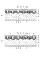
図2は、半導体装置100を模式的に示す平面図である。
図2(a)に示すように、半導体装置100は、ドレイン端子26にボンディングされた半導体チップ90の表面に、ゲート端子25とソース端子27がボンディングされた構成を有している。ゲート端子25の接続部25aと、ソース端子27の接続部27aは、それぞれ平板状の形状を有しており、所謂ダイレクトリード接続が設けられている。ドレイン端子26と半導体チップ90の裏面は、ドレイン電極17を介して電気的に接続される。FIG. 2 is a plan view schematically showing the
As shown in FIG. 2A, the
図2(a)に示すI−I断面は、図1に示した断面構造を有しており、ゲート端子25の接続部25aと半導体チップ90との間は、接着層23によって接続されている。接着層23には、例えば、ハンダ材を用いることができる。
一方、ソース端子27の接続部27aも、同じように接着層23を介して半導体チップ90の表面に接続することができる。そして、ソース端子27とソース電極12との間は、電気的に接続される。2A has the cross-sectional structure shown in FIG. 1, and the
On the other hand, the
図2(b)は、ゲート端子25の接続部25aと接触する半導体チップ90の一部を模式的に示す平面図である。同図中に示す波線で囲まれた領域25bが、接続部25aと接触する部分である。 FIG. 2B is a plan view schematically showing a part of the
本実施形態に係る半導体装置100では、ゲート端子25が接触する部分に一体のゲート電極パッドが設けられる訳ではなく、図1および図2(b)に示すように、複数のゲート引き出し電極13が相互に離間して設けられる。そして、ゲート引き出し電極13の上に設けられたコンタクト電極21および接着層23を介して、ゲート端子25の接続部25aとゲート引き出し電極13とが電気的に接続される構成となっている。 In the
図2(b)に示す例では、領域25bの内部に8個のゲート引き出し電極13が設けられているが、例えば、ゲート引き出し電極13は、少なくとも2つ以上あればよく、ゲート電流に応じた数およびサイズを選択することができる。そして、図2(b)中には、正方形の接着層23およびゲート引き出し電極13が示されているが、これも正方形に限定されるものではなく、長方形、円形等、様々な形状とすることができる。 In the example shown in FIG. 2B, eight
さらに、例えば、図2(b)に示した8個の接着層23の全てが、ゲート引き出し電極13に電気的に接続されている必要はなく、その一部は、ゲート端子25の接着強度を確保するために、絶縁性保護膜15の表面に設けられても良い。 Further, for example, it is not necessary that all of the eight
ゲート引き出し電極13のサイズおよび数は、ゲート電流の最大値を勘案して、必要最小限に決定することができる。ゲート電流は、半導体装置100をスイッチング制御する場合の過渡電流であり、その値は小さい。したがって、例えば、複数のゲート引き出し電極13の総面積を、領域25bに含まれるソース電極12の面積よりも狭くすることができる。 The size and number of the
本実施形態に係る半導体装置100では、図1に示すように、ゲート端子25の接続部25aがボンディングされる領域25b(図2(b)参照)においても、p形ベース領域3およびn形ソース領域4、ゲート電極7が設けられチャネルが形成される。さらに、ソース電極12も、p形ベース領域3およびn形ソース領域4に接続されて設けられることから、領域25b以外の素子部10と同じようにオン電流を流すことができる。 In the
したがって、半導体装置100におけるオン電流が流れる有効領域の面積を拡大することができるので、オン抵抗Ronを低減することが可能であり、Ronとチップ面積Sの積Ron×Sを小さくすることができる。 Therefore, since the area of the effective region in which the on-current flows in the
さらに、ゲート引き出し電極13は、複数形成することができるため、個々のゲート引き出し電極13の面積を、ゲート端子25の接続部25aの面積よりも大幅に縮小することが可能である。これにより、例えば、ゲート引き出し電極13の下に位置するn形ドリフト層2で発生するホールに対し、ソース電極12に直接接続されないp形ベース領域3およびp+コンタクト領域5を介した排出抵抗を小さくすることができる。そして、ゲート端子25の接続部25aにおけるアバランシェ降伏を抑制して、アバランシェ耐量を向上させ、あるいは、電流集中による破壊を防ぐことができる。Furthermore, since a plurality of
なお、上記のように、ゲート引き出し電極13のサイズを縮小した場合には、ゲート引き出し電極13の下にn形ソース領域4を含まない構成、すなわち、ゲート電極7の下にチャネルのない構成とすることもできる。 As described above, when the size of the
以下、図3〜図9を参照して、半導体装置100の製造過程を説明する。
図3(a)は、n形ドリフト層2の表面にゲート絶縁膜6となる絶縁膜6aを形成し、ゲート電極となる導電層7aを形成した状態を模式的に示す断面図である。Hereinafter, the manufacturing process of the
FIG. 3A is a cross-sectional view schematically showing a state in which an insulating
n形ドリフト層2は、例えば、n形不純物を高濃度にドープしたシリコン基板の上に形成することができる。絶縁膜6aには、熱酸化膜(SiO2膜)を用いることができ、導電層7aには、ポリシリコンを用いることができる。The n-
次に、図3(b)は、導電層7aをパターニングしてゲート電極7が形成された状態を示している。
続いて、図3(c)に示すように、ゲート電極7の表面に絶縁膜31を形成する。例えば、ポリシリコンの表面を熱酸化してSiO2膜を形成することができる。Next, FIG. 3B shows a state in which the
Subsequently, as shown in FIG. 3C, an insulating
図4(a)は、n形ドリフト層2の表面にp形ベース領域3が形成された状態を模式的に示す断面図である。
例えば、ゲート電極7をマスクとして、n形ドリフト層2の表面にp形不純物をイオン注入し、その後、熱処理を施してp形不純物を拡散させることができる。p形不純物としてボロン(B)を用いることができる。FIG. 4A is a cross-sectional view schematically showing a state where the p-
For example, p-type impurities can be ion-implanted into the surface of the n-
次に、図4(b)に示すように、p形ベース領域3の表面に、n形ソース領域4とp+コンタクト領域5とを形成する。
例えば、n形不純物である砒素(As)およびp形不純物であるBを、それぞれ選択的にイオン注入することにより、n形ソース領域4およびp+コンタクト領域5を形成することができる。Next, as shown in FIG. 4B, an n-
For example, n-
図5は、図4に続く製造過程を示し、n形ソース領域4およびp+コンタクト領域5と、ゲート電極7と、にコンタクトするための開口を、層間絶縁膜33に形成する工程を模式的に示した断面図である。
図5(a)に示すように、層間絶縁膜33の上に、開口41aを有するレジストマスク41を形成する。続いて、例えば、ドライエッチング法を用いて、層間絶縁膜33をエッチングする。FIG. 5 shows a manufacturing process subsequent to FIG. 4 and schematically shows a process of forming an opening in the
As shown in FIG. 5A, a resist
図5(b)は、開口33aおよび開口33bが層間絶縁膜33に形成され、レジストマスク41が除去された状態を示している。開口33aは、ソース電極12をn形ソース領域4およびp+コンタクト領域5にコンタクトさせるために形成されている。一方、ゲート引き出し電極13が形成される領域(図6(b)参照)には、ゲート電極7にコンタクトするための開口33bのみが形成され、n形ソース領域およびp+コンタクト領域に連通する開口は形成されない。FIG. 5B shows a state in which the
図6は、図5に続く製造過程を示し、ソース電極12およびゲート引き出し電極13を形成する工程を模式的に示した断面図である。
図6(a)に示すように、開口33aおよび33bが形成された層間絶縁膜33の上に電極メタル36が形成される。例えば、スパッタ法を用いてアルミニウム(Al)膜を形成することができる。FIG. 6 is a cross-sectional view schematically showing a process of forming the
As shown in FIG. 6A, an
続いて、図6(b)に示すように、電極メタル36をパターニングし、ソース電極12とゲート引き出し電極13とに分離する。ソース電極12は、開口33aを介してn形ソース領域4とp+コンタクト領域5とに接触している。一方、ゲート引き出し電極13は、開口33bを介してゲート電極7に接触している。
このように、本実施形態に係る半導体装置100の製造方法では、ソース電極12とゲート引き出し電極13とを、p形ベース領域3、n形ソース領域4およびゲート電極7の上に同時に形成することができる。Subsequently, as shown in FIG. 6B, the
As described above, in the method for manufacturing the
図7は、図6に示す製造過程に続き、ソース電極12およびゲート引き出し電極13の上に絶縁性保護膜15が形成された状態を示している。
絶縁性保護膜15は、半導体チップ90の表面を保護するとともに、ゲート端子25とソース電極12との間に介在し、両者を絶縁する。絶縁性保護膜15として、例えば、ポリイミド膜を用いることができる。FIG. 7 shows a state in which the insulating
The insulating
絶縁性保護膜15には、複数のコンタクトホール15aが形成される(図2(b)参照)。さらに、ソース端子27とソース電極12との間を電気的に接続するためのコンタクトホール15bを形成しても良い(図9参照)。 A plurality of
続いて、図8に示すように、コンタクトホール15aおよび15bの内部に、コンタクト電極21と、接着層23とが形成される。
コンタクト電極21は、例えば、ニッケル(Ni)電極であり、メッキ法を用いて形成することができる。
接着層23には、例えば、ゲート端子25およびソース端子27を接着するためのハンダ材を用いることができる。Subsequently, as shown in FIG. 8, a
The
For the
コンタクトホール15aは、ゲート引き出し電極13の内側にコンタクト電極21が接触するように、ゲート引き出し電極13よりも小さなサイズの開口に形成することができる。
例えば、接着層23がハンダ材である場合、Niを用いたコンタクト電極21は、ハンダのマイグレーションを防ぐバリア層として機能する。さらに、図8中に示すように、コンタクト電極21をゲート引き出し電極13の内側に接触するように形成することにより、コンタクト電極21と絶縁性保護膜15との界面を伝って進入するハンダ材を、ゲート引き出し電極13の表面で止めることが可能となる。The
For example, when the
次に、図2に示すように、半導体チップ90が基板から切り出され、ドレイン端子26の上にボンディングされる。そして、ゲート端子25およびソース端子27が、それぞれ半導体チップ90の表面にボンディングされる。 Next, as shown in FIG. 2, the
そして、図9に示すように、ゲート端子25の接続部25a、および、ソース端子27の接続部27aが、接着層23およびコンタクト電極21を介して、ゲート引き出し電極13およびソース電極12にそれぞれ接続される。 As shown in FIG. 9, the connecting
本実施形態に係る半導体装置100では、接続部25aの下にもn形ソース領域4およびp+コンタクト領域5に接続されたソース電極12が設けられ、絶縁性保護膜15により接続部25aと絶縁されている。In the
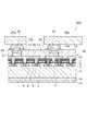
図10は、本実施形態の変形例に係る半導体装置200の断面を示す模式図である。
半導体装置200は、ゲート端子25の接続部25aおよびソース端子27の接続部27aを、金属バンプ42を用いてコンタクト電極21に接続した点において、半導体装置100と相違する。金属バンプ42には、例えば、ハンダボールを用いることができる。FIG. 10 is a schematic diagram illustrating a cross section of a
The
絶縁性保護膜15のコンタクトホール15aおよび15bの内部に設けられたコンタクト電極21の上には、バンプ電極43が設けられている。バンプ電極43は、例えば、Ni膜を用いて形成することができる。 A
バンプ電極43の中央には、コンタクトホール15aおよび15bの開口に対応した窪みがあり、例えば、ボール状の金属バンプ42をコンタクトホール15aおよび15bの開口上にガイドすることができる。
そして、コンタクトホール15aおよび15bの開口上に位置した金属バンプ42の上から、ゲート端子25の接続部25aと、ソース端子27の接続部27aと、を熱圧着させることにより、半導体チップ90の表面に接続することができる。In the center of the
Then, the surface of the
以上、本発明に係る一実施形態を参照して本発明を説明したが、本発明はこれらの実施形態に限定されるものではない。例えば、出願時の技術水準に基づいて、当業者がなし得る設計変更や、材料の変更等、本発明と技術的思想を同じとする実施態様も本発明の技術的範囲に含有される。 As mentioned above, although this invention was demonstrated with reference to one embodiment which concerns on this invention, this invention is not limited to these embodiment. For example, embodiments that have the same technical idea as the present invention, such as design changes and material changes that can be made by those skilled in the art based on the technical level at the time of filing, are also included in the technical scope of the present invention.
例えば、本実施形態に係る半導体装置100および200では、所謂、縦型プレーナゲート型パワーMOSFETを例示しているが、トレンチゲート構造を有するMOSFETであっても良いし、IGBT等の他のスイッチングデバイスであっても良い。さらに、横型のデバイス構造にも適用することができる。また、GaNやSiCといったシリコン以外の材料を用いたデバイスに適用することもできる。 For example, in the
本実施形態は、ゲート端子25をゲート電極7に電気的に接続する構成を例として説明したが、ゲート電極7への接続に限らず、他の部分への接続であっても、オン電流が流れない領域を有効領域として活用するために適用することが可能である。 In the present embodiment, the configuration in which the
2・・・n形ドリフト層、 3・・・p形ベース領域、 4・・・n形ソース領域、 5・・・p+コンタクト領域、 6・・・ゲート絶縁膜、 6a、31・・・絶縁膜、 7・・・ゲート電極、 7a・・・導電層、 10・・・素子部、 12・・・ソース電極、 12a・・・フィールドプレート、 13・・・ゲート引き出し電極、 15・・・絶縁性保護膜、 15a、15b・・・コンタクトホール、 16・・・ドレイン層、 17・・・ドレイン電極、 18・・・ガードリング、 20・・・終端部、 21・・・コンタクト電極、 23・・・接着層、 24・・・フィールド酸化膜、 25・・・ゲート端子、 25a、27a・・・接続部、 26・・・ドレイン端子、 27・・・ソース端子、 33・・・層間絶縁膜、 33a、33b、41a・・・開口、 36・・・電極メタル、 41・・・レジストマスク、 42・・・金属バンプ、 43・・・バンプ電極、 90・・・半導体チップ、 100、200・・・半導体装置2 ... n-type drift layer, 3 ... p-type base region, 4 ... n-type source region, 5 ... p+ contact region, 6 ... gate insulating film, 6a, 31 ... Insulating film, 7 ... Gate electrode, 7a ... Conductive layer, 10 ... Element part, 12 ... Source electrode, 12a ... Field plate, 13 ... Gate extraction electrode, 15 ... Insulating protective film, 15a, 15b ... contact hole, 16 ... drain layer, 17 ... drain electrode, 18 ... guard ring, 20 ... termination, 21 ... contact electrode, 23 ... Adhesion layer, 24 ... Field oxide film, 25 ... Gate terminal, 25a, 27a ... Connection, 26 ... Drain terminal, 27 ... Source terminal, 33 ... Interlayer insulation Membrane, 33a, 33b, 41a ... opening, 36 ... metal electrode, 41 ... resist
Claims (5)
Translated fromJapanese前記第1の半導体領域との間に第1の絶縁膜を介して設けられた制御電極と、
前記制御電極に電気的に接続された引き出し電極と、
前記主電極および前記引き出し電極の上に設けられた第2の絶縁膜と、
前記第2の絶縁膜に形成された複数のコンタクトホールの内部に設けられ、前記引き出し電極に電気的に接続された複数のコンタクト電極と、
前記主電極のうちの前記第1の半導体領域の上と前記第2の半導体領域の上と前記制御電極の上とに設けられた部分と、前記引き出し電極と、を覆い、前記複数のコンタクト電極に電気的に接続され、前記第2の絶縁膜により前記主電極から電気的に絶縁された制御端子と、
を備えたことを特徴とする半導体装置。A main electrode electrically connected to a first semiconductor region of a first conductivity type and a second semiconductor region of a second conductivity type selectively provided on a surface of the first semiconductor region;
A control electrode provided between the first semiconductor region via a first insulating film;
An extraction electrode electrically connected to the control electrode;
A second insulating film provided on the main electrode and the lead electrode;
A plurality of contact electrodes provided in the plurality of contact holes formed in the second insulating film and electrically connected to the lead electrodes;
A plurality of contact electrodes covering a portion of the main electrode provided on the first semiconductor region, the second semiconductor region, and the control electrode, and the lead electrode; A control terminal electrically connected to the main electrode by the second insulating film; and
A semiconductor device comprising:
前記第1の半導体領域との間に第1の絶縁膜を介して設けられた制御電極と、
前記制御電極に電気的に接続された引き出し電極と、
前記主電極および前記引き出し電極の上に設けられた第2の絶縁膜と、
前記主電極の一部および前記引き出し電極を覆って制御端子がボンディングされる領域において、前記第2の絶縁膜に形成された複数のコンタクトホールの内部に設けられ、前記制御端子と前記引き出し電極とを電気的に接続する複数のコンタクト電極と、
を有する半導体装置の製造方法であって、
前記第1の半導体領域、前記第2の半導体領域および前記制御電極の上に、前記主電極および前記引き出し電極となる金属膜を同時に形成することを特徴とする半導体装置の製造方法。A main electrode electrically connected to a first semiconductor region of a first conductivity type and a second semiconductor region of a second conductivity type selectively provided on a surface of the first semiconductor region;
A control electrode provided between the first semiconductor region via a first insulating film;
An extraction electrode electrically connected to the control electrode;
A second insulating film provided on the main electrode and the lead electrode;
In a region where the control terminal is bonded to cover a part of the main electrode and the extraction electrode, the control terminal and the extraction electrode are provided inside a plurality of contact holes formed in the second insulating film. A plurality of contact electrodes for electrically connecting,
A method of manufacturing a semiconductor device having
A method of manufacturing a semiconductor device, wherein a metal film to be the main electrode and the lead electrode is simultaneously formed on the first semiconductor region, the second semiconductor region, and the control electrode.
Priority Applications (3)
| Application Number | Priority Date | Filing Date | Title |
|---|---|---|---|
| JP2010210134AJP2012064899A (en) | 2010-09-17 | 2010-09-17 | Semiconductor device and method of manufacturing the same |
| CN2011100668673ACN102412273A (en) | 2010-09-17 | 2011-03-18 | Semiconductor device and manufacturing method thereof |
| US13/052,908US20120068258A1 (en) | 2010-09-17 | 2011-03-21 | Semiconductor device and method for manufacturing same |
Applications Claiming Priority (1)
| Application Number | Priority Date | Filing Date | Title |
|---|---|---|---|
| JP2010210134AJP2012064899A (en) | 2010-09-17 | 2010-09-17 | Semiconductor device and method of manufacturing the same |
Publications (1)
| Publication Number | Publication Date |
|---|---|
| JP2012064899Atrue JP2012064899A (en) | 2012-03-29 |
Family
ID=45816973
Family Applications (1)
| Application Number | Title | Priority Date | Filing Date |
|---|---|---|---|
| JP2010210134APendingJP2012064899A (en) | 2010-09-17 | 2010-09-17 | Semiconductor device and method of manufacturing the same |
Country Status (3)
| Country | Link |
|---|---|
| US (1) | US20120068258A1 (en) |
| JP (1) | JP2012064899A (en) |
| CN (1) | CN102412273A (en) |
Cited By (4)
| Publication number | Priority date | Publication date | Assignee | Title |
|---|---|---|---|---|
| WO2014156791A1 (en)* | 2013-03-29 | 2014-10-02 | 富士電機株式会社 | Semiconductor device and manufacturing method for semiconductor device |
| JP2019047045A (en)* | 2017-09-05 | 2019-03-22 | 富士電機株式会社 | Silicon carbide semiconductor device and silicon carbide semiconductor device manufacturing method |
| JP2022527399A (en)* | 2019-04-11 | 2022-06-01 | ウルフスピード インコーポレイテッド | Transistor semiconductor die with increased working area |
| US12074079B2 (en) | 2019-04-11 | 2024-08-27 | Wolfspeed, Inc. | Wide bandgap semiconductor device with sensor element |
Families Citing this family (5)
| Publication number | Priority date | Publication date | Assignee | Title |
|---|---|---|---|---|
| JP5452195B2 (en) | 2009-12-03 | 2014-03-26 | 株式会社 日立パワーデバイス | Semiconductor device and power conversion device using the same |
| US8643071B2 (en)* | 2012-06-14 | 2014-02-04 | Alpha And Omega Semiconductor Incorporated | Integrated snubber in a single poly MOSFET |
| JP2017059636A (en)* | 2015-09-15 | 2017-03-23 | 三菱電機株式会社 | Method for manufacturing semiconductor device |
| CN110890278B (en)* | 2018-09-10 | 2024-02-23 | 上海先进半导体制造有限公司 | Method for improving yield of planar IGBT and intermediate product for manufacturing same |
| JP7472435B2 (en) | 2019-05-13 | 2024-04-23 | 富士電機株式会社 | Semiconductor module manufacturing method |
Citations (6)
| Publication number | Priority date | Publication date | Assignee | Title |
|---|---|---|---|---|
| JPS62224074A (en)* | 1986-03-26 | 1987-10-02 | Hitachi Ltd | Insulated gate semiconductor device |
| JPH0394472A (en)* | 1989-09-06 | 1991-04-19 | Matsushita Electron Corp | Vertical type mos field-effect transistor |
| JPH04239137A (en)* | 1991-01-11 | 1992-08-27 | Nec Corp | Vertical type field effect transistor |
| JPH10233509A (en)* | 1997-02-12 | 1998-09-02 | Motorola Semiconducteurs Sa | Semiconductor power devices |
| JP2009105177A (en)* | 2007-10-23 | 2009-05-14 | Shindengen Electric Mfg Co Ltd | Semiconductor device |
| JP2010165880A (en)* | 2009-01-16 | 2010-07-29 | Toyota Industries Corp | Semiconductor device |
Family Cites Families (7)
| Publication number | Priority date | Publication date | Assignee | Title |
|---|---|---|---|---|
| US5589783A (en)* | 1994-07-29 | 1996-12-31 | Sgs-Thomson Microelectronics, Inc. | Variable input threshold adjustment |
| US6689680B2 (en)* | 2001-07-14 | 2004-02-10 | Motorola, Inc. | Semiconductor device and method of formation |
| US6617696B1 (en)* | 2002-03-14 | 2003-09-09 | Fairchild Semiconductor Corporation | Supporting control gate connection on a package using additional bumps |
| US7910471B2 (en)* | 2004-02-02 | 2011-03-22 | Texas Instruments Incorporated | Bumpless wafer scale device and board assembly |
| US7560808B2 (en)* | 2005-10-19 | 2009-07-14 | Texas Instruments Incorporated | Chip scale power LDMOS device |
| US7944048B2 (en)* | 2006-08-09 | 2011-05-17 | Monolithic Power Systems, Inc. | Chip scale package for power devices and method for making the same |
| US8395191B2 (en)* | 2009-10-12 | 2013-03-12 | Monolithic 3D Inc. | Semiconductor device and structure |
- 2010
- 2010-09-17JPJP2010210134Apatent/JP2012064899A/enactivePending
- 2011
- 2011-03-18CNCN2011100668673Apatent/CN102412273A/enactivePending
- 2011-03-21USUS13/052,908patent/US20120068258A1/ennot_activeAbandoned
Patent Citations (6)
| Publication number | Priority date | Publication date | Assignee | Title |
|---|---|---|---|---|
| JPS62224074A (en)* | 1986-03-26 | 1987-10-02 | Hitachi Ltd | Insulated gate semiconductor device |
| JPH0394472A (en)* | 1989-09-06 | 1991-04-19 | Matsushita Electron Corp | Vertical type mos field-effect transistor |
| JPH04239137A (en)* | 1991-01-11 | 1992-08-27 | Nec Corp | Vertical type field effect transistor |
| JPH10233509A (en)* | 1997-02-12 | 1998-09-02 | Motorola Semiconducteurs Sa | Semiconductor power devices |
| JP2009105177A (en)* | 2007-10-23 | 2009-05-14 | Shindengen Electric Mfg Co Ltd | Semiconductor device |
| JP2010165880A (en)* | 2009-01-16 | 2010-07-29 | Toyota Industries Corp | Semiconductor device |
Cited By (8)
| Publication number | Priority date | Publication date | Assignee | Title |
|---|---|---|---|---|
| WO2014156791A1 (en)* | 2013-03-29 | 2014-10-02 | 富士電機株式会社 | Semiconductor device and manufacturing method for semiconductor device |
| US10355089B2 (en) | 2013-03-29 | 2019-07-16 | Fuji Electric Co., Ltd. | Semiconductor device and semiconductor device manufacturing method |
| JP2019047045A (en)* | 2017-09-05 | 2019-03-22 | 富士電機株式会社 | Silicon carbide semiconductor device and silicon carbide semiconductor device manufacturing method |
| JP7013735B2 (en) | 2017-09-05 | 2022-02-01 | 富士電機株式会社 | Silicon Carbide Semiconductor Device and Method for Manufacturing Silicon Carbide Semiconductor Device |
| JP2022527399A (en)* | 2019-04-11 | 2022-06-01 | ウルフスピード インコーポレイテッド | Transistor semiconductor die with increased working area |
| JP7422166B2 (en) | 2019-04-11 | 2024-01-25 | ウルフスピード インコーポレイテッド | Transistor semiconductor die with increased active area |
| US12057389B2 (en) | 2019-04-11 | 2024-08-06 | Wolfspeed, Inc. | Transistor semiconductor die with increased active area |
| US12074079B2 (en) | 2019-04-11 | 2024-08-27 | Wolfspeed, Inc. | Wide bandgap semiconductor device with sensor element |
Also Published As
| Publication number | Publication date |
|---|---|
| US20120068258A1 (en) | 2012-03-22 |
| CN102412273A (en) | 2012-04-11 |
Similar Documents
| Publication | Publication Date | Title |
|---|---|---|
| JP2012064899A (en) | Semiconductor device and method of manufacturing the same | |
| US10672878B2 (en) | Silicon carbide semiconductor device | |
| WO2014163058A1 (en) | Semiconductor device | |
| JP2003224273A (en) | Semiconductor device | |
| JP2006173437A (en) | Semiconductor device | |
| CN109564942A (en) | Semiconductor device | |
| US11489047B2 (en) | Semiconductor device and method of manufacturing the same | |
| JP2020191441A (en) | Manufacturing method of super-junction semiconductor device and super-junction semiconductor device | |
| JP7302285B2 (en) | semiconductor equipment | |
| US11177360B2 (en) | Semiconductor device | |
| US10256232B2 (en) | Semiconductor device including a switching element and a sense diode | |
| JP5601863B2 (en) | Power semiconductor device | |
| JPH04251983A (en) | semiconductor equipment | |
| JPWO2017208735A1 (en) | Semiconductor device | |
| JP2021197384A (en) | Semiconductor device | |
| US11043557B2 (en) | Semiconductor device | |
| US11133385B2 (en) | Semiconductor device | |
| JP2009099911A (en) | Semiconductor device | |
| JP4764998B2 (en) | Semiconductor device | |
| JP2022042526A (en) | Semiconductor device | |
| JP2012004466A (en) | Semiconductor device | |
| JP6177300B2 (en) | Semiconductor device | |
| US11245031B2 (en) | Semiconductor device | |
| JP7472613B2 (en) | Semiconductor Device | |
| JP7275572B2 (en) | Semiconductor device and method for manufacturing semiconductor device |
Legal Events
| Date | Code | Title | Description |
|---|---|---|---|
| A621 | Written request for application examination | Free format text:JAPANESE INTERMEDIATE CODE: A621 Effective date:20120816 | |
| A977 | Report on retrieval | Free format text:JAPANESE INTERMEDIATE CODE: A971007 Effective date:20130121 | |
| A131 | Notification of reasons for refusal | Free format text:JAPANESE INTERMEDIATE CODE: A131 Effective date:20130123 | |
| A521 | Request for written amendment filed | Free format text:JAPANESE INTERMEDIATE CODE: A523 Effective date:20130319 | |
| A131 | Notification of reasons for refusal | Free format text:JAPANESE INTERMEDIATE CODE: A131 Effective date:20131030 | |
| A02 | Decision of refusal | Free format text:JAPANESE INTERMEDIATE CODE: A02 Effective date:20140304 |