JP2012064562A - Lamp device - Google Patents
Lamp deviceDownload PDFInfo
- Publication number
- JP2012064562A JP2012064562AJP2011151734AJP2011151734AJP2012064562AJP 2012064562 AJP2012064562 AJP 2012064562AJP 2011151734 AJP2011151734 AJP 2011151734AJP 2011151734 AJP2011151734 AJP 2011151734AJP 2012064562 AJP2012064562 AJP 2012064562A
- Authority
- JP
- Japan
- Prior art keywords
- substrate
- lamp device
- pins
- heat
- opening
- Prior art date
- Legal status (The legal status is an assumption and is not a legal conclusion. Google has not performed a legal analysis and makes no representation as to the accuracy of the status listed.)
- Granted
Links
Images


Classifications
- F—MECHANICAL ENGINEERING; LIGHTING; HEATING; WEAPONS; BLASTING
- F21—LIGHTING
- F21V—FUNCTIONAL FEATURES OR DETAILS OF LIGHTING DEVICES OR SYSTEMS THEREOF; STRUCTURAL COMBINATIONS OF LIGHTING DEVICES WITH OTHER ARTICLES, NOT OTHERWISE PROVIDED FOR
- F21V29/00—Protecting lighting devices from thermal damage; Cooling or heating arrangements specially adapted for lighting devices or systems
- F21V29/50—Cooling arrangements
- F21V29/70—Cooling arrangements characterised by passive heat-dissipating elements, e.g. heat-sinks
- F21V29/74—Cooling arrangements characterised by passive heat-dissipating elements, e.g. heat-sinks with fins or blades
- F21V29/77—Cooling arrangements characterised by passive heat-dissipating elements, e.g. heat-sinks with fins or blades with essentially identical diverging planar fins or blades, e.g. with fan-like or star-like cross-section
- G—PHYSICS
- G02—OPTICS
- G02B—OPTICAL ELEMENTS, SYSTEMS OR APPARATUS
- G02B6/00—Light guides; Structural details of arrangements comprising light guides and other optical elements, e.g. couplings
- G02B6/0001—Light guides; Structural details of arrangements comprising light guides and other optical elements, e.g. couplings specially adapted for lighting devices or systems
- G02B6/0005—Light guides; Structural details of arrangements comprising light guides and other optical elements, e.g. couplings specially adapted for lighting devices or systems the light guides being of the fibre type
- G02B6/0008—Light guides; Structural details of arrangements comprising light guides and other optical elements, e.g. couplings specially adapted for lighting devices or systems the light guides being of the fibre type the light being emitted at the end of the fibre
- F—MECHANICAL ENGINEERING; LIGHTING; HEATING; WEAPONS; BLASTING
- F21—LIGHTING
- F21V—FUNCTIONAL FEATURES OR DETAILS OF LIGHTING DEVICES OR SYSTEMS THEREOF; STRUCTURAL COMBINATIONS OF LIGHTING DEVICES WITH OTHER ARTICLES, NOT OTHERWISE PROVIDED FOR
- F21V17/00—Fastening of component parts of lighting devices, e.g. shades, globes, refractors, reflectors, filters, screens, grids or protective cages
- F21V17/10—Fastening of component parts of lighting devices, e.g. shades, globes, refractors, reflectors, filters, screens, grids or protective cages characterised by specific fastening means or way of fastening
- F—MECHANICAL ENGINEERING; LIGHTING; HEATING; WEAPONS; BLASTING
- F21—LIGHTING
- F21V—FUNCTIONAL FEATURES OR DETAILS OF LIGHTING DEVICES OR SYSTEMS THEREOF; STRUCTURAL COMBINATIONS OF LIGHTING DEVICES WITH OTHER ARTICLES, NOT OTHERWISE PROVIDED FOR
- F21V29/00—Protecting lighting devices from thermal damage; Cooling or heating arrangements specially adapted for lighting devices or systems
- F21V29/50—Cooling arrangements
- F21V29/70—Cooling arrangements characterised by passive heat-dissipating elements, e.g. heat-sinks
- F21V29/74—Cooling arrangements characterised by passive heat-dissipating elements, e.g. heat-sinks with fins or blades
- F21V29/77—Cooling arrangements characterised by passive heat-dissipating elements, e.g. heat-sinks with fins or blades with essentially identical diverging planar fins or blades, e.g. with fan-like or star-like cross-section
- F21V29/773—Cooling arrangements characterised by passive heat-dissipating elements, e.g. heat-sinks with fins or blades with essentially identical diverging planar fins or blades, e.g. with fan-like or star-like cross-section the planes containing the fins or blades having the direction of the light emitting axis
- F—MECHANICAL ENGINEERING; LIGHTING; HEATING; WEAPONS; BLASTING
- F21—LIGHTING
- F21V—FUNCTIONAL FEATURES OR DETAILS OF LIGHTING DEVICES OR SYSTEMS THEREOF; STRUCTURAL COMBINATIONS OF LIGHTING DEVICES WITH OTHER ARTICLES, NOT OTHERWISE PROVIDED FOR
- F21V2200/00—Use of light guides, e.g. fibre optic devices, in lighting devices or systems
- F21V2200/10—Use of light guides, e.g. fibre optic devices, in lighting devices or systems of light guides of the optical fibres type
- F21V2200/13—Use of light guides, e.g. fibre optic devices, in lighting devices or systems of light guides of the optical fibres type the light being emitted at the end of the guide
- F—MECHANICAL ENGINEERING; LIGHTING; HEATING; WEAPONS; BLASTING
- F21—LIGHTING
- F21Y—INDEXING SCHEME ASSOCIATED WITH SUBCLASSES F21K, F21L, F21S and F21V, RELATING TO THE FORM OR THE KIND OF THE LIGHT SOURCES OR OF THE COLOUR OF THE LIGHT EMITTED
- F21Y2115/00—Light-generating elements of semiconductor light sources
- F21Y2115/10—Light-emitting diodes [LED]
- G—PHYSICS
- G02—OPTICS
- G02B—OPTICAL ELEMENTS, SYSTEMS OR APPARATUS
- G02B6/00—Light guides; Structural details of arrangements comprising light guides and other optical elements, e.g. couplings
- G02B6/0001—Light guides; Structural details of arrangements comprising light guides and other optical elements, e.g. couplings specially adapted for lighting devices or systems
- G02B6/0005—Light guides; Structural details of arrangements comprising light guides and other optical elements, e.g. couplings specially adapted for lighting devices or systems the light guides being of the fibre type
- G02B6/0006—Coupling light into the fibre
Landscapes
- Engineering & Computer Science (AREA)
- General Engineering & Computer Science (AREA)
- Physics & Mathematics (AREA)
- General Physics & Mathematics (AREA)
- Optics & Photonics (AREA)
- Arrangement Of Elements, Cooling, Sealing, Or The Like Of Lighting Devices (AREA)
- Non-Portable Lighting Devices Or Systems Thereof (AREA)
- Fastening Of Light Sources Or Lamp Holders (AREA)
Abstract
Translated fromJapaneseDescription
Translated fromJapanese実施例は、ランプ装置に関するものである。The embodiment relates to a lamp device.
LED(light emitting diode)は、電気エネルギーを光エネルギーに変換するエネルギー変換素子であって、発光素子は蛍光灯、白熱灯等の既存の光源に比べて低消費電力、半永久的な寿命、速い応答速度、安全性、環境親和性の長所を有する。
従って、既存の光源を発光素子に代替するための多くの研究が進行されており、既に発光素子は室内外で用いられる各種の液晶表示装置、電光板、街灯、表示灯、室内灯等の照明装置の光源として使用が増加されている成り行きである。LED (light emitting diode) is an energy conversion element that converts electrical energy into light energy. Has the advantages of speed, safety and environmental friendliness.
Accordingly, much research has been conducted to replace existing light sources with light-emitting elements, and the light-emitting elements have already been used for lighting of various liquid crystal display devices, electric boards, street lamps, indicator lamps, indoor lamps and the like used indoors and outdoors. This is the result of increasing use as a light source for devices.
実施例のランプ装置の目的は、ランプ装置の駆動時に発生する熱を効率的に放出することである。 The purpose of the lamp device of the embodiment is to efficiently release the heat generated when the lamp device is driven.
実施例のランプ装置の他の目的は、ランプ装置の部品に問題がある場合、容易に維持補修することがである。 Another purpose of the lamp device of the embodiment is to easily maintain and repair the lamp device when there is a problem.
実施例のランプ装置のさらに他の目的は、体積をスリム化して空間的な制約に係わらず、設置自由度を向上させることである。 Still another object of the lamp device of the embodiment is to reduce the volume and improve the degree of freedom of installation regardless of the spatial constraints.
一実施例によるランプ装置は、開口部を形成するように内面と外面を有する構造体と、前記構造体の外面から外部方向に延長された複数のピンを含む放熱体;前記放熱体の複数のピンの下部に配置され、一面に配置された複数の発光素子を有する基板を含む。 A lamp device according to an embodiment includes a heat dissipation body including a structure having an inner surface and an outer surface so as to form an opening, and a plurality of pins extending outward from the outer surface of the structure; The substrate includes a plurality of light emitting elements disposed under the pins and disposed on one surface.
一実施例による他のランプ装置は、開口部を形成するように内面と外面を有する構造体と、前記構造体の外面から外部方向に延長された複数のピンと、前記複数のピンの一端が連結された平面部を含む放熱体;前記放熱体の平面部上に配置され、上面を有する基板;及び前記基板の上面と反対に位置する下面に配置された複数の発光素子を含む。 Another lamp device according to an embodiment includes a structure having an inner surface and an outer surface so as to form an opening, a plurality of pins extending outward from the outer surface of the structure, and one end of the plurality of pins connected to each other. A heat dissipating body including the planar portion; a substrate disposed on the planar portion of the heat dissipating body and having an upper surface; and a plurality of light emitting elements disposed on a lower surface opposite to the upper surface of the substrate.
一実施例によるまた他のランプ装置は、開口部を形成するように内面と外面を有する構造体と、前記構造体の外面から外部方向に延長された複数のピンを含む放熱体;及び前記放熱体の複数のピンの下部に配置され、一面に配置された複数の発光素子と、複数のホールを有する基板を含み、前記放熱体の複数のピンのうち隣り合う二つのピンは間隔を置いて離隔されている。 According to another embodiment of the present invention, there is provided a heat dissipation body including a structure having an inner surface and an outer surface so as to form an opening, and a plurality of pins extending outward from the outer surface of the structure; A plurality of light emitting elements disposed on a single surface and a substrate having a plurality of holes, and two adjacent pins among the plurality of pins of the radiator are spaced apart from each other Are separated.
実施例のランプ装置によれば、ランプ装置の駆動時に発生する熱を効率的に放出することができる。 According to the lamp device of the embodiment, the heat generated when the lamp device is driven can be efficiently released.
実施例のランプ装置によれば、ランプ装置の部品に問題がある場合、容易に維持補修することができる。 According to the lamp device of the embodiment, if there is a problem with the components of the lamp device, it can be easily maintained and repaired.
実施例のランプ装置によれば、体積をスリム化して空間的な制約に係わらず、設置自由度を向上させることができる。 According to the lamp device of the embodiment, it is possible to improve the degree of freedom of installation regardless of spatial restrictions by reducing the volume.
本発明による実施例の説明において、各エレメントの“上又は下(on or under)”に形成されるものと記載される場合において、上又は下は、2つのエレメントが互いに直接(directly)接触されるか、1つ以上の他のエレメントが上記2つのエレメントの間に配置されて(indirectly)形成されることを全て含む。また、“上又は下”と表現される場合、1つのエレメントを基準に上方向だけでなく下方向の意味も含むことができる。 In the description of the embodiment according to the invention, where it is stated that it is formed “on or under” each element, the top or bottom is where the two elements are in direct contact with each other. Or one or more other elements are all formed indirectly between the two elements. In addition, when expressed as “up or down”, it can include not only an upward direction but also a downward direction based on one element.
以下、添付された図面を参照して実施例を詳しく説明することとする。 Hereinafter, embodiments will be described in detail with reference to the accompanying drawings.
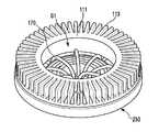
図1は、本発明の一実施例によるランプ装置の斜視図であり、図2は、図1に示された本発明の一実施例によるランプ装置の断面斜視図であり、図3は、図1に示された本発明の一実施例によるランプ装置の分解斜視図である。 FIG. 1 is a perspective view of a lamp device according to an embodiment of the present invention, FIG. 2 is a cross-sectional perspective view of the lamp device according to an embodiment of the present invention shown in FIG. 1, and FIG. 1 is an exploded perspective view of a lamp device according to an embodiment of the present invention shown in FIG.
図1乃至図3を参照すると、本発明の一実施例によるランプ装置100は、放熱体110、基板130、光源部150、光ガイド170、フランジ190、第1部材210、集光レンズ220、第2部材230及び固定部材250を含む。 1 to 3, a
放熱体110は、リング形状の構造体111と、複数のピン113、平面部115が有機的に結合されて全体形状がドーナツ形態をなす。しかし、放熱体は実施例に限定されず、例えば、構造体の場合、多角形状やその他の多様な形状を有することができる。 The heat dissipating body 110 has a ring-
リング構造体111は、中心軸Aを有する開口部G1が中央に形成されるように内面と外面を有する。複数のピン113はリング構造体111の外面に結合され、前記リング構造体111の外面から外部方向に放射状に延長される。複数のピン113は、後述する光源部150から発生した熱が全体的に均一に外部に放出されるように一定の間隔で維持され得る。平面部115は前記リング構造体111の外面の一端に結合され、前記リング構造体111の外面に垂直延長され、前記リング構造体111の外面に結合された複数のピン113の一端と結合される。 The
基板130は、放熱体の平面部115と隣接した上面と光源部150が配置される下面を有する。このような基板130は、一般的に用いられる金属印刷回路基板(Printed Circuit Board)を主に用いることが望ましいが、その他、光源部が配置され得る基板であれば、いずれでも使用可能である。 The
基板130は、開口部G1を有するリング構造体111を密閉するように一つの円板形状を有することができるが、光源部150から発生した熱が空気の循環を通じて外部に放出され得るように、中央に開口部G2を有することが望ましい。また、基板中央の開口部G2は同一の中心軸Aを有するように放熱体の開口部G1と対応するように位置される。この時、基板中央の開口部G2と放熱体の開口部G1は、ランプ装置の組み立て性や放熱特性を向上させるために同一の面積を有することが望ましい。 The
光源部150は複数の発光ダイオード(LED)を含み、複数の発光ダイオードは基板の下面に放射状に配置される。即ち、複数の発光ダイオードは、複数のピン113の配列方法のように等間隔で基板130の下面に配列され得る。 The
このように、複数の発光ダイオードが基板に放射状に配置されると、発光ダイオードが動作時に発生する熱の放出面積が広くなり、熱放出効率が高くなる。また、発光ダイオードの熱は放熱体の平面部と基板の上面と接触されて放出され、放熱体の複数のピンを通じて放出されることで放熱表面積の増大により熱伝逹特性が向上する。 As described above, when a plurality of light emitting diodes are arranged radially on the substrate, a heat emission area generated by the light emitting diodes during operation is widened, and heat emission efficiency is increased. Further, the heat of the light emitting diode is released in contact with the flat portion of the radiator and the upper surface of the substrate, and is released through a plurality of pins of the radiator, thereby improving the heat transfer characteristics by increasing the heat radiation surface area.
また、図面には示されていないが、基板130と放熱体110の平面部115との間に放熱のための伝導性シートがさらに加えられて、基板130と放熱体110との間の熱的伝達特性を向上させることができる。 Further, although not shown in the drawing, a conductive sheet for heat dissipation is further added between the
また、複数の発光ダイオードが個別基板ではなく一つの基板に実装されて配置され、必要時に光源部を含む基板の維持補修が容易である。 In addition, a plurality of light emitting diodes are mounted and arranged on a single substrate instead of an individual substrate, and it is easy to maintain and repair the substrate including the light source unit when necessary.
光ガイド170は複数の光ファイバーからなり、各光ファイバーの一端は前記複数の発光ダイオード150に光学的に結合される。本実施例では光ガイド170は光ファイバーを例示として挙げたが、光学装置のようなプリズムのように光源部から発生した光を所望の方向に切り替えることができる装置であれば、いずれでも可能である。 The
フランジ190は、前記複数の光ファイバーが挿入されてその末端を結合するための複数のホール191を有し、全体外形は円板形状を有する。よって、フランジ190によって前記複数の発光ダイオードが結合されることにより、放射状に配置された複数の発光ダイオードから発生した光出射領域が減るようになって、光が特定の方向に集光される。 The
フランジ190のホール191に挿入された前記複数の光ファイバーの末端は、同一平面に位置されるようにフランジのホール191に位置決めされる。これは、光が入射される特定の面で均一な光強度を有するようにするためである。また、フランジは、後で説明する第1部材210の開口部G3に安着されて第1部材210の調節角度によって、発生する光について特定の指向面を形成することができるようになる。 The ends of the plurality of optical fibers inserted into the
第1部材210は、中心軸を有する円形開口部G3が中央に形成されるように内面と外面を有する第1リング構造体211と第1突出部212及び第2突出部213を含む。第1突出部212と第2突出部213は互いに向かい合うように第1リング構造体211の外面に結合され、第1突出部212と第2突出部213は第1リング構造体211の外面で外部方向に延長されて配置される。第1部材の第1突出部212と第2突出部213それぞれは、後で説明する第2部材230の第1ホール231aと第2ホール231bにそれぞれ挿入され、第1部材210は第2部材230に挟んで結合される。 The
このような第1部材210は、第1突出部212と第2突出部213が軸になり、角度を有して回転可能に傾く。従って、使用者が所望の方向に第1部材210の傾斜角を調節して光源部150から発生した光について特定の指向性を設定することができるようになる。 The
集光レンズ220は第1部材210と光学的に結合され、フランジ190が安着される第1部材の円形開口部の反対側の開口部を覆う。このような集光レンズは、フランジによって物理的に集光された光を光学的にさらに集光するようになる。 The
第2部材230は、第1部材210と同様に、中心軸を有する円形開口部G4が中央に形成されるように内面と外面を有する第2リング構造体231と第1突出部232及び第2突出部233を含む。また、第2部材230は、前記第1部材210の第1突出部212と第2突出部213が挿入されるために第2リング構造体231の内面と外面を貫通し、互いに向かい合う第1ホール231aと第2ホール231bを含む。第1突出部232と第2突出部233は、第2リング構造体231の外面で外部方向に延長されて配置される。 Similar to the
このような第2部材230は、第1突出部232から水平延長されて第2突出部233に水平に至るまでの第1仮想ラインと、第2部材の第1ホール231aの中心軸が延長されて第2ホール231bの中心軸に至るまでの第2仮想ラインが交差される時、二つの仮想ラインが交差されてなす角は直角をなす構造である。 The
第2部材230の内面の円周の長さは第1部材210の外面の円周の長さよりさらに大きく形成されて第1部材210が第2部材230に挿入される。 The circumferential length of the inner surface of the
固定部材250は、中心軸を有する円形開口部G5が形成されるように内周部251を有し、前記内周部251から間隔を置いて前記内周部に沿って配置された外周部253及び前記内周部の末端で垂直方向に延長されて前記外周部の末端に連結される平面部255を含む。 The fixing
固定部材250の内周部251は、前記第2部材230の第1突出部232と第2突出部233が挿入されるために互いに向かい合う第1ホール251aと第2ホール251bを含む。第2部材230の第1突出部232と第2突出部233が前記固定部材250の第1ホール251aと第2ホール251bにそれぞれ挿入され、前記第2部材230は前記固定部材250の内周部251の内面に挟んで結合される。 The inner
固定部材250の外周部253は前記光源部150と光ガイド170を囲む。 An outer
上記のようなランプ装置は、駆動時に発光ダイオードから発生した熱を空間的に上下方向ではなく水平方向に放出できる構造を有する放熱体を含んでおり、実質的にランプ装置全体の体積スリム化を来たし得る。従って、ランプ装置の設置時、上下方向に熱を放出する従来の放熱体に比べて空間的な制約をより少なく受けるようになる。従って、設置自由度を向上させることができる。 The lamp device as described above includes a heat radiating body having a structure capable of releasing heat generated from the light-emitting diodes in the horizontal direction instead of the vertical direction during driving, and substantially reducing the volume of the entire lamp device. You can come. Therefore, when the lamp device is installed, it is less subject to spatial restrictions than the conventional heat radiator that emits heat in the vertical direction. Accordingly, the degree of freedom in installation can be improved.
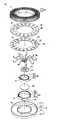
図4は、本発明の一実施例による他のランプ装置の斜視図であり、図5は、図4に示された本発明の一実施例によるランプ装置の分解斜視図である。 4 is a perspective view of another lamp apparatus according to an embodiment of the present invention, and FIG. 5 is an exploded perspective view of the lamp apparatus according to an embodiment of the present invention shown in FIG.
図4乃至図5を参照すると、本発明の一実施例による他のランプ装置300は、放熱体310、放熱板330、基板350、光源部370、光ガイド390、フランジ410、第1部材430、第2部材450及び固定部材470を含む。 4 to 5, another
放熱体310はリング形状を有する構造体311と、複数のピン313が有機的に結合されて全体形状がドーナツ形態をなす。しかし、放熱体は実施例に限定されず、例えば、構造体の場合、多角形状やその他の多様な形状を有し得る。リング構造体311は、中心軸Aを有する開口部G1’が中央に形成されるように内面と外面を有する。複数のピン313は、リング構造体311の外面に結合され、前記リング構造体311の外面から外部方向に放射状に延長される。後述する光源部370から発生した熱が全体的に均一に外部に放出されるように複数のピン313の間隔は一定に維持される。即ち、隣り合う二つのピンは一定の間隔を置いて配置され得る。 The
放熱板330は、複数のピン313のうち隣り合う二つのピンの間の間隔に対応する領域にホール331を有し、放射状に配置された複数のピン313と隣接して配置される。また、放熱板330は前記放熱体310の中央開口部G1’に対応するように中央に開口部G2’を有する。放熱板330のホール331は、前記放熱体の上部で外部空気の流入がさらに円滑になるように前記ピンの長さ方向に実質的に平行な長方形構造を有する。このような放熱板330は、基板が直接放熱体の複数のピンと接触する場合、省略され得る。また、放熱板330と放熱体310が一体型をなして実質的に図3に示された放熱体110からなり得る。即ち、放熱板330は図3の放熱体110の平面部115の役割をすることができる。 The
基板350は、放熱板330と隣接した上面と光源部370が配置される下面を有する。このような基板350は、一般的に用いられる金属印刷回路基板(Printed Circuit Board)を主に用いることが望ましいが、その他、光源部が配置され得る基板であれば、いずれでも使用可能である。 The
基板350は、開口部G2’を有する放熱板330を密閉するように密閉された一つの円板形状を有し得るが、光源部370から発生した熱が外部空気の循環を通じて外部に放出され得るように、中央に開口部G3’を有することが望ましい。この時、基板350の中央の開口部G3’は、放熱板330の開口部G2’と対応するように位置される。また、基板350は複数のホール351を有し、前記複数のホール351は、基板の下面に配置される光源部370の間に位置する。 The
さらに望ましくは、基板のホール351は、光源部370の間に配列されながら前記放熱板330のホール331と対応する位置に配列される。基板のホール351も放熱板330のホール331のような長方形構造を有する。 More preferably, the
図面には示されていないが、基板350は、放熱板なしに前記放熱体の複数のピンに直接接触して熱伝達をすることができ、放熱体と放熱板との間、あるいは放熱板と基板との間に放熱のための伝導性シートが加えられて、放熱体と放熱板あるいは放熱板と基板との間の熱的伝達特性を向上させることができる。 Although not shown in the drawings, the
光源部370は複数の発光ダイオード(LED)を含み、複数の発光ダイオードは基板の下面に放射状に延長されて配置される。即ち、複数の発光ダイオードは、前記放熱体310の複数のピン313の配列方法と対応するように基板350の下面に配列される。 The
このように、複数の発光ダイオードが基板に放射状に配置されると、発光ダイオードが動作時に発生する熱の放出面積が広くなり、熱放出効率が高くなる。また、発光ダイオードの熱は、基板のホールや放熱板のホールを通じて空気の循環により放熱され得、放熱体の複数のピンを通じて放熱表面積の増大により熱伝逹特性が向上する。また、図面には示されていないが、基板と放熱板との間に放熱のための伝導性シートがさらに加えられて基板と放熱板との間の熱的伝達特性を向上させることができる。 As described above, when a plurality of light emitting diodes are arranged radially on the substrate, a heat emission area generated by the light emitting diodes during operation is widened, and heat emission efficiency is increased. The heat of the light emitting diode can be dissipated by air circulation through the hole of the substrate or the hole of the heat sink, and the heat transfer characteristics are improved by increasing the heat dissipating surface area through the plurality of pins of the heat dissipator. Further, although not shown in the drawings, a conductive sheet for heat dissipation is further added between the substrate and the heat radiating plate, so that the thermal transfer characteristics between the substrate and the heat radiating plate can be improved.
また、複数の発光ダイオードが個別基板ではなく一つの基板に実装されて配置され、必要時に光源部を含む基板の維持補修が容易である。 In addition, a plurality of light emitting diodes are mounted and arranged on a single substrate instead of an individual substrate, and it is easy to maintain and repair the substrate including the light source unit when necessary.
残りの光ガイド390、フランジ410、第1部材430、集光レンズ440、第2部材450及び固定部材470は、前の本発明の一実施例で説明した内容と類似するため、これについての説明は省略することとする。 The remaining
以上において実施例に説明された特徴、構造、効果等は、本発明の少なくとも一つの実施例に含まれ、必ずしも一つの実施例のみに限定されるものではない。延いては、各実施例において例示された特徴、構造、効果等は、実施例の属する分野における通常の知識を有する者によって他の実施例に対しても組み合わせ又は変形されて実施可能である。従って、このような組み合わせと変形に係る内容は、本発明の範囲に含まれるものと解釈されなければならない。 The features, structures, effects, and the like described in the embodiments above are included in at least one embodiment of the present invention, and are not necessarily limited to only one embodiment. By extension, the features, structures, effects, and the like exemplified in each embodiment can be combined with or modified by other persons having ordinary knowledge in the field to which the embodiment belongs. Accordingly, the contents related to such combinations and modifications should be construed as being included in the scope of the present invention.
また、以上において実施例を中心に説明したが、これは単に例示であるだけで本発明を限定するものではなく、本発明の属する分野における通常の知識を有する者であれば、本実施例の本質的な特性から外れない範囲で以上に例示されていない様々な変形と応用が可能なことが分かる。例えば、実施例に具体的に示された各構成要素は変形して実施できるものである。そして、このような変形と応用に係る相違点は、添付された請求の範囲において規定する本発明の範囲に含まれるものと解釈されなければならない。
Further, although the embodiment has been mainly described above, this is merely an example and does not limit the present invention. Any person having ordinary knowledge in the field to which the present invention belongs can be used. It will be understood that various modifications and applications not exemplified above are possible without departing from the essential characteristics. For example, each component specifically shown in the embodiment can be modified and implemented. Such differences in modification and application should be construed as being included in the scope of the present invention as defined in the appended claims.
Claims (20)
Translated fromJapanese前記放熱体の複数のピンの下部に配置され、一面に配置された複数の発光素子を有する基板を含むことを特徴とするランプ装置。A heat dissipating member including a structure having an inner surface and an outer surface so as to form an opening, and a plurality of pins extending outward from the outer surface of the structure;
A lamp device comprising: a substrate having a plurality of light emitting elements disposed on one surface and disposed under a plurality of pins of the heat dissipating body.
前記放熱板は、前記基板と面接触することを特徴とする請求項1に記載のランプ装置。A heat sink having an opening corresponding to the opening of the heat dissipator between the plurality of pins of the heat dissipator and the substrate;
The lamp device according to claim 1, wherein the heat radiating plate is in surface contact with the substrate.
前記放熱板は、前記二つのピンの間の間隔に対応する領域にホールを有し、一面が前記複数のピンと接触することを特徴とする請求項5に記載のランプ装置。Two adjacent pins among the plurality of pins of the heat dissipating body are separated by a predetermined interval,
The lamp device according to claim 5, wherein the heat radiating plate has a hole in a region corresponding to a distance between the two pins, and one surface is in contact with the plurality of pins.
前記放熱体の平面部上に配置され、上面を有する基板;及び
前記基板の上面と反対に位置する下面に配置された複数の発光素子を含むことを特徴とするランプ装置。A heat radiating body including a structure having an inner surface and an outer surface so as to form an opening, a plurality of pins extending outward from the outer surface of the structure, and a planar portion to which one end of the plurality of pins is connected;
A lamp device comprising: a substrate disposed on a planar portion of the radiator and having an upper surface; and a plurality of light emitting elements disposed on a lower surface opposite to the upper surface of the substrate.
前記放熱体の複数のピンの下部に配置され、一面に配置された複数の発光素子と、複数のホールを有する基板を含み、
前記放熱体の複数のピンのうち隣り合う二つのピンは間隔を置いて離隔されていることを特徴とするランプ装置。A heat sink including a structure having an inner surface and an outer surface so as to form an opening, and a plurality of pins extending outward from the outer surface of the structure; and disposed below the plurality of pins of the heat radiator, Including a plurality of light emitting elements arranged on one surface and a substrate having a plurality of holes;
Two adjacent pins among the plurality of pins of the heat dissipating member are spaced apart from each other.
The lamp of claim 18, further comprising a heat radiating plate positioned between the substrate and the heat radiating body to conduct heat generated from the plurality of light emitting devices of the substrate to the heat radiating body. apparatus.
Applications Claiming Priority (2)
| Application Number | Priority Date | Filing Date | Title |
|---|---|---|---|
| KR10-2010-0091547 | 2010-09-17 | ||
| KR1020100091547AKR101742678B1 (en) | 2010-09-17 | 2010-09-17 | Lamp apparatus |
Related Child Applications (1)
| Application Number | Title | Priority Date | Filing Date |
|---|---|---|---|
| JP2016001095ADivisionJP6196330B2 (en) | 2010-09-17 | 2016-01-06 | Lamp device |
Publications (3)
| Publication Number | Publication Date |
|---|---|
| JP2012064562Atrue JP2012064562A (en) | 2012-03-29 |
| JP2012064562A5 JP2012064562A5 (en) | 2014-08-21 |
| JP5868622B2 JP5868622B2 (en) | 2016-02-24 |
Family
ID=43929048
Family Applications (2)
| Application Number | Title | Priority Date | Filing Date |
|---|---|---|---|
| JP2011151734AExpired - Fee RelatedJP5868622B2 (en) | 2010-09-17 | 2011-07-08 | Lamp device |
| JP2016001095AActiveJP6196330B2 (en) | 2010-09-17 | 2016-01-06 | Lamp device |
Family Applications After (1)
| Application Number | Title | Priority Date | Filing Date |
|---|---|---|---|
| JP2016001095AActiveJP6196330B2 (en) | 2010-09-17 | 2016-01-06 | Lamp device |
Country Status (5)
| Country | Link |
|---|---|
| US (1) | US8476813B2 (en) |
| EP (2) | EP2511606B1 (en) |
| JP (2) | JP5868622B2 (en) |
| KR (1) | KR101742678B1 (en) |
| CN (1) | CN102410515B (en) |
Families Citing this family (6)
| Publication number | Priority date | Publication date | Assignee | Title |
|---|---|---|---|---|
| USD671257S1 (en)* | 2010-04-10 | 2012-11-20 | Lg Innotek Co., Ltd. | LED lamp |
| US8297790B2 (en)* | 2010-08-18 | 2012-10-30 | Lg Innotek Co., Ltd. | Lamp device |
| KR101742678B1 (en) | 2010-09-17 | 2017-06-01 | 엘지이노텍 주식회사 | Lamp apparatus |
| CN102606950B (en)* | 2012-03-02 | 2013-11-27 | 中山伟强科技有限公司 | A kind of LED projection lamp |
| CN103411186A (en)* | 2013-08-10 | 2013-11-27 | 无锡市宝成塑胶科技有限公司 | Thermally-conductive resin lamp holder for LED panel lamps |
| KR102116272B1 (en) | 2017-04-21 | 2020-05-29 | 주식회사 케이엠더블유 | Multiple input multiple output antenna apparatus |
Citations (6)
| Publication number | Priority date | Publication date | Assignee | Title |
|---|---|---|---|---|
| JP2007005058A (en)* | 2005-06-22 | 2007-01-11 | Matsushita Electric Works Ltd | Luminaire |
| JP2007095684A (en)* | 2005-09-26 | 2007-04-12 | Osram Sylvania Inc | LED lamps using direct optical coupling in an axial arrangement |
| JP2007513378A (en)* | 2003-12-02 | 2007-05-24 | スリーエム イノベイティブ プロパティズ カンパニー | Solid state optical device |
| US20080049399A1 (en)* | 2006-07-12 | 2008-02-28 | Hong Kong Applied Science And Technology Research Institute Co., Ltd. | Lighting device |
| WO2009044716A1 (en)* | 2007-10-01 | 2009-04-09 | Koha Co., Ltd. | Light emitting device |
| WO2010089397A1 (en)* | 2009-02-09 | 2010-08-12 | Osram Gesellschaft mit beschränkter Haftung | Cooling element for a lighting device |
Family Cites Families (17)
| Publication number | Priority date | Publication date | Assignee | Title |
|---|---|---|---|---|
| JPH11202164A (en)* | 1998-01-19 | 1999-07-30 | Toyoda Gosei Co Ltd | Optical source module |
| JP3066834U (en)* | 1999-08-23 | 2000-03-07 | 株式会社遠藤照明 | Recessed ceiling light with replaceable lighting unit |
| US6371628B1 (en)* | 2000-02-03 | 2002-04-16 | Lucifer Lighting Company | Post-installation adjustable lighting fixture |
| JP2002367406A (en) | 2001-06-05 | 2002-12-20 | Algol:Kk | Ring-like led lighting system |
| US6832849B2 (en) | 2001-12-04 | 2004-12-21 | Ccs, Inc. | Light radiation device, light source device, light radiation unit, and light connection mechanism |
| JP3966845B2 (en)* | 2003-09-29 | 2007-08-29 | 株式会社松村電機製作所 | LED lighting device |
| BRPI0417183A (en)* | 2003-12-02 | 2007-03-06 | 3M Innovative Properties Co | irradiation apparatus, irradiation system and system |
| US7258474B2 (en) | 2005-04-21 | 2007-08-21 | Magna International Inc. | Headlamp with beam patterns formed from semiconductor light sources |
| US7431475B2 (en) | 2005-07-22 | 2008-10-07 | Sony Corporation | Radiator for light emitting unit, and backlight device |
| US8789962B2 (en)* | 2005-10-27 | 2014-07-29 | Vikon Surgical, Llc | Surgical headlight |
| CN201028412Y (en)* | 2006-12-29 | 2008-02-27 | 梁立人 | Turning lamp |
| US7458706B1 (en)* | 2007-11-28 | 2008-12-02 | Fu Zhun Precision Industry (Shen Zhen) Co., Ltd. | LED lamp with a heat sink |
| JP2009140718A (en)* | 2007-12-05 | 2009-06-25 | Toshiba Lighting & Technology Corp | Lighting device |
| US7682049B2 (en)* | 2008-04-15 | 2010-03-23 | Fu Zhun Precision Industry (Shen Zhen) Co., Ltd. | LED lamp |
| JP2010108792A (en)* | 2008-10-30 | 2010-05-13 | Toshiba Lighting & Technology Corp | Luminaire |
| IT1392500B1 (en) | 2008-12-30 | 2012-03-09 | I B T S P A | LED DISSIPATION OPTIMIZED HEAT LIGHTING DEVICE FOR OUTDOOR AND LARGE COVERED AREAS |
| KR101742678B1 (en) | 2010-09-17 | 2017-06-01 | 엘지이노텍 주식회사 | Lamp apparatus |
- 2010
- 2010-09-17KRKR1020100091547Apatent/KR101742678B1/ennot_activeExpired - Fee Related
- 2011
- 2011-02-08EPEP12176009.4Apatent/EP2511606B1/ennot_activeNot-in-force
- 2011-02-08EPEP11153747Apatent/EP2431660B1/ennot_activeNot-in-force
- 2011-03-04USUS13/040,779patent/US8476813B2/ennot_activeExpired - Fee Related
- 2011-03-22CNCN201110072437.2Apatent/CN102410515B/ennot_activeExpired - Fee Related
- 2011-07-08JPJP2011151734Apatent/JP5868622B2/ennot_activeExpired - Fee Related
- 2016
- 2016-01-06JPJP2016001095Apatent/JP6196330B2/enactiveActive
Patent Citations (7)
| Publication number | Priority date | Publication date | Assignee | Title |
|---|---|---|---|---|
| JP2007513378A (en)* | 2003-12-02 | 2007-05-24 | スリーエム イノベイティブ プロパティズ カンパニー | Solid state optical device |
| JP2007005058A (en)* | 2005-06-22 | 2007-01-11 | Matsushita Electric Works Ltd | Luminaire |
| JP2007095684A (en)* | 2005-09-26 | 2007-04-12 | Osram Sylvania Inc | LED lamps using direct optical coupling in an axial arrangement |
| US20080049399A1 (en)* | 2006-07-12 | 2008-02-28 | Hong Kong Applied Science And Technology Research Institute Co., Ltd. | Lighting device |
| WO2009044716A1 (en)* | 2007-10-01 | 2009-04-09 | Koha Co., Ltd. | Light emitting device |
| WO2010089397A1 (en)* | 2009-02-09 | 2010-08-12 | Osram Gesellschaft mit beschränkter Haftung | Cooling element for a lighting device |
| JP2012517659A (en)* | 2009-02-09 | 2012-08-02 | オスラム アクチエンゲゼルシャフト | Cooling body for lighting device |
Also Published As
| Publication number | Publication date |
|---|---|
| CN102410515A (en) | 2012-04-11 |
| JP2016042492A (en) | 2016-03-31 |
| EP2431660A1 (en) | 2012-03-21 |
| JP5868622B2 (en) | 2016-02-24 |
| US20110204764A1 (en) | 2011-08-25 |
| EP2431660B1 (en) | 2012-11-07 |
| US8476813B2 (en) | 2013-07-02 |
| JP6196330B2 (en) | 2017-09-13 |
| EP2511606B1 (en) | 2014-01-15 |
| EP2511606A1 (en) | 2012-10-17 |
| CN102410515B (en) | 2014-06-11 |
| KR20120029632A (en) | 2012-03-27 |
| KR101742678B1 (en) | 2017-06-01 |
Similar Documents
| Publication | Publication Date | Title |
|---|---|---|
| US8419220B2 (en) | Lamp device | |
| JP6196330B2 (en) | Lamp device | |
| JP5706536B2 (en) | LED lighting fixtures | |
| TWI361260B (en) | ||
| CN101566325B (en) | Light-emitting diode lamp | |
| US7997768B2 (en) | LED lamp | |
| KR20120017234A (en) | Lamp unit | |
| CN101660737A (en) | Light emitting diode (LED) lamp | |
| CN103423613A (en) | Light emitting diode lamp | |
| KR200463715Y1 (en) | Assembling structure of the illuminators for medical usage | |
| KR100960735B1 (en) | Illuminator having led lens | |
| JP2014143161A (en) | Light projector | |
| KR101742679B1 (en) | Lamp apparatus | |
| TWI396809B (en) | Led lamp | |
| KR101752421B1 (en) | Lamp apparatus | |
| KR101761384B1 (en) | Lamp apparatus | |
| US20120057343A1 (en) | Illuminating apparatus having heat dissipation base and multilayer array-type led module | |
| TWI397652B (en) | Led lamp | |
| KR101883323B1 (en) | Lighting device | |
| KR101823135B1 (en) | Lighting device | |
| TWI399505B (en) | Led lamp | |
| KR100943521B1 (en) | Floodlight-floodlight device easy heat emission | |
| JP2012160259A (en) | Led lighting apparatus | |
| TWM415263U (en) | Lamp |
Legal Events
| Date | Code | Title | Description |
|---|---|---|---|
| RD03 | Notification of appointment of power of attorney | Free format text:JAPANESE INTERMEDIATE CODE: A7423 Effective date:20130319 | |
| RD04 | Notification of resignation of power of attorney | Free format text:JAPANESE INTERMEDIATE CODE: A7424 Effective date:20130514 | |
| A521 | Request for written amendment filed | Free format text:JAPANESE INTERMEDIATE CODE: A523 Effective date:20140708 | |
| A621 | Written request for application examination | Free format text:JAPANESE INTERMEDIATE CODE: A621 Effective date:20140708 | |
| A131 | Notification of reasons for refusal | Free format text:JAPANESE INTERMEDIATE CODE: A131 Effective date:20150414 | |
| A521 | Request for written amendment filed | Free format text:JAPANESE INTERMEDIATE CODE: A523 Effective date:20150706 | |
| A131 | Notification of reasons for refusal | Free format text:JAPANESE INTERMEDIATE CODE: A131 Effective date:20150804 | |
| A521 | Request for written amendment filed | Free format text:JAPANESE INTERMEDIATE CODE: A523 Effective date:20151029 | |
| TRDD | Decision of grant or rejection written | ||
| A01 | Written decision to grant a patent or to grant a registration (utility model) | Free format text:JAPANESE INTERMEDIATE CODE: A01 Effective date:20151208 | |
| A61 | First payment of annual fees (during grant procedure) | Free format text:JAPANESE INTERMEDIATE CODE: A61 Effective date:20160106 | |
| R150 | Certificate of patent or registration of utility model | Ref document number:5868622 Country of ref document:JP Free format text:JAPANESE INTERMEDIATE CODE: R150 | |
| R250 | Receipt of annual fees | Free format text:JAPANESE INTERMEDIATE CODE: R250 | |
| R250 | Receipt of annual fees | Free format text:JAPANESE INTERMEDIATE CODE: R250 | |
| R250 | Receipt of annual fees | Free format text:JAPANESE INTERMEDIATE CODE: R250 | |
| S531 | Written request for registration of change of domicile | Free format text:JAPANESE INTERMEDIATE CODE: R313531 | |
| S111 | Request for change of ownership or part of ownership | Free format text:JAPANESE INTERMEDIATE CODE: R313113 | |
| R350 | Written notification of registration of transfer | Free format text:JAPANESE INTERMEDIATE CODE: R350 | |
| R350 | Written notification of registration of transfer | Free format text:JAPANESE INTERMEDIATE CODE: R350 | |
| R250 | Receipt of annual fees | Free format text:JAPANESE INTERMEDIATE CODE: R250 | |
| R250 | Receipt of annual fees | Free format text:JAPANESE INTERMEDIATE CODE: R250 | |
| LAPS | Cancellation because of no payment of annual fees |