JP2012063528A - Reflection type color display element and color display device - Google Patents
Reflection type color display element and color display deviceDownload PDFInfo
- Publication number
- JP2012063528A JP2012063528AJP2010206896AJP2010206896AJP2012063528AJP 2012063528 AJP2012063528 AJP 2012063528AJP 2010206896 AJP2010206896 AJP 2010206896AJP 2010206896 AJP2010206896 AJP 2010206896AJP 2012063528 AJP2012063528 AJP 2012063528A
- Authority
- JP
- Japan
- Prior art keywords
- hue
- hue element
- liquid crystal
- layer
- color display
- Prior art date
- Legal status (The legal status is an assumption and is not a legal conclusion. Google has not performed a legal analysis and makes no representation as to the accuracy of the status listed.)
- Pending
Links
Images


Classifications
- G—PHYSICS
- G02—OPTICS
- G02F—OPTICAL DEVICES OR ARRANGEMENTS FOR THE CONTROL OF LIGHT BY MODIFICATION OF THE OPTICAL PROPERTIES OF THE MEDIA OF THE ELEMENTS INVOLVED THEREIN; NON-LINEAR OPTICS; FREQUENCY-CHANGING OF LIGHT; OPTICAL LOGIC ELEMENTS; OPTICAL ANALOGUE/DIGITAL CONVERTERS
- G02F1/00—Devices or arrangements for the control of the intensity, colour, phase, polarisation or direction of light arriving from an independent light source, e.g. switching, gating or modulating; Non-linear optics
- G02F1/01—Devices or arrangements for the control of the intensity, colour, phase, polarisation or direction of light arriving from an independent light source, e.g. switching, gating or modulating; Non-linear optics for the control of the intensity, phase, polarisation or colour
- G02F1/13—Devices or arrangements for the control of the intensity, colour, phase, polarisation or direction of light arriving from an independent light source, e.g. switching, gating or modulating; Non-linear optics for the control of the intensity, phase, polarisation or colour based on liquid crystals, e.g. single liquid crystal display cells
- G02F1/137—Devices or arrangements for the control of the intensity, colour, phase, polarisation or direction of light arriving from an independent light source, e.g. switching, gating or modulating; Non-linear optics for the control of the intensity, phase, polarisation or colour based on liquid crystals, e.g. single liquid crystal display cells characterised by the electro-optical or magneto-optical effect, e.g. field-induced phase transition, orientation effect, guest-host interaction or dynamic scattering
- G02F1/13718—Devices or arrangements for the control of the intensity, colour, phase, polarisation or direction of light arriving from an independent light source, e.g. switching, gating or modulating; Non-linear optics for the control of the intensity, phase, polarisation or colour based on liquid crystals, e.g. single liquid crystal display cells characterised by the electro-optical or magneto-optical effect, e.g. field-induced phase transition, orientation effect, guest-host interaction or dynamic scattering based on a change of the texture state of a cholesteric liquid crystal
- G—PHYSICS
- G02—OPTICS
- G02F—OPTICAL DEVICES OR ARRANGEMENTS FOR THE CONTROL OF LIGHT BY MODIFICATION OF THE OPTICAL PROPERTIES OF THE MEDIA OF THE ELEMENTS INVOLVED THEREIN; NON-LINEAR OPTICS; FREQUENCY-CHANGING OF LIGHT; OPTICAL LOGIC ELEMENTS; OPTICAL ANALOGUE/DIGITAL CONVERTERS
- G02F1/00—Devices or arrangements for the control of the intensity, colour, phase, polarisation or direction of light arriving from an independent light source, e.g. switching, gating or modulating; Non-linear optics
- G02F1/01—Devices or arrangements for the control of the intensity, colour, phase, polarisation or direction of light arriving from an independent light source, e.g. switching, gating or modulating; Non-linear optics for the control of the intensity, phase, polarisation or colour
- G02F1/13—Devices or arrangements for the control of the intensity, colour, phase, polarisation or direction of light arriving from an independent light source, e.g. switching, gating or modulating; Non-linear optics for the control of the intensity, phase, polarisation or colour based on liquid crystals, e.g. single liquid crystal display cells
- G02F1/133—Constructional arrangements; Operation of liquid crystal cells; Circuit arrangements
- G02F1/1333—Constructional arrangements; Manufacturing methods
- G02F1/1347—Arrangement of liquid crystal layers or cells in which the final condition of one light beam is achieved by the addition of the effects of two or more layers or cells
- G02F1/13471—Arrangement of liquid crystal layers or cells in which the final condition of one light beam is achieved by the addition of the effects of two or more layers or cells in which all the liquid crystal cells or layers remain transparent, e.g. FLC, ECB, DAP, HAN, TN, STN, SBE-LC cells
- G02F1/13473—Arrangement of liquid crystal layers or cells in which the final condition of one light beam is achieved by the addition of the effects of two or more layers or cells in which all the liquid crystal cells or layers remain transparent, e.g. FLC, ECB, DAP, HAN, TN, STN, SBE-LC cells for wavelength filtering or for colour display without the use of colour mosaic filters
- G—PHYSICS
- G09—EDUCATION; CRYPTOGRAPHY; DISPLAY; ADVERTISING; SEALS
- G09G—ARRANGEMENTS OR CIRCUITS FOR CONTROL OF INDICATING DEVICES USING STATIC MEANS TO PRESENT VARIABLE INFORMATION
- G09G2300/00—Aspects of the constitution of display devices
- G09G2300/02—Composition of display devices
- G09G2300/023—Display panel composed of stacked panels
- G—PHYSICS
- G09—EDUCATION; CRYPTOGRAPHY; DISPLAY; ADVERTISING; SEALS
- G09G—ARRANGEMENTS OR CIRCUITS FOR CONTROL OF INDICATING DEVICES USING STATIC MEANS TO PRESENT VARIABLE INFORMATION
- G09G2300/00—Aspects of the constitution of display devices
- G09G2300/04—Structural and physical details of display devices
- G09G2300/0439—Pixel structures
- G09G2300/0452—Details of colour pixel setup, e.g. pixel composed of a red, a blue and two green components
- G—PHYSICS
- G09—EDUCATION; CRYPTOGRAPHY; DISPLAY; ADVERTISING; SEALS
- G09G—ARRANGEMENTS OR CIRCUITS FOR CONTROL OF INDICATING DEVICES USING STATIC MEANS TO PRESENT VARIABLE INFORMATION
- G09G3/00—Control arrangements or circuits, of interest only in connection with visual indicators other than cathode-ray tubes
- G09G3/20—Control arrangements or circuits, of interest only in connection with visual indicators other than cathode-ray tubes for presentation of an assembly of a number of characters, e.g. a page, by composing the assembly by combination of individual elements arranged in a matrix no fixed position being assigned to or needed to be assigned to the individual characters or partial characters
- G09G3/34—Control arrangements or circuits, of interest only in connection with visual indicators other than cathode-ray tubes for presentation of an assembly of a number of characters, e.g. a page, by composing the assembly by combination of individual elements arranged in a matrix no fixed position being assigned to or needed to be assigned to the individual characters or partial characters by control of light from an independent source
- G09G3/36—Control arrangements or circuits, of interest only in connection with visual indicators other than cathode-ray tubes for presentation of an assembly of a number of characters, e.g. a page, by composing the assembly by combination of individual elements arranged in a matrix no fixed position being assigned to or needed to be assigned to the individual characters or partial characters by control of light from an independent source using liquid crystals
- G09G3/3611—Control of matrices with row and column drivers
- G09G3/3622—Control of matrices with row and column drivers using a passive matrix
- G09G3/3629—Control of matrices with row and column drivers using a passive matrix using liquid crystals having memory effects, e.g. ferroelectric liquid crystals
Landscapes
- Physics & Mathematics (AREA)
- Nonlinear Science (AREA)
- Chemical & Material Sciences (AREA)
- Crystallography & Structural Chemistry (AREA)
- General Physics & Mathematics (AREA)
- Optics & Photonics (AREA)
- Liquid Crystal (AREA)
- Devices For Indicating Variable Information By Combining Individual Elements (AREA)
- Optical Filters (AREA)
Abstract
Translated fromJapaneseDescription
Translated fromJapanese本発明は、反射型カラー表示素子およびカラー表示装置に関する。 The present invention relates to a reflective color display element and a color display device.
近年、各企業・大学で電子ペーパーの開発が盛んに進められている。電子ペーパーが期待されている応用市場として、電子書籍を筆頭として、モバイル端末のサブディスプレイやICカードの表示部など、多用な応用携帯が提案されている。 In recent years, development of electronic paper has been actively promoted at various companies and universities. As an application market in which electronic paper is expected, various applied mobile phones such as a sub display of a mobile terminal and a display unit of an IC card have been proposed, starting with an electronic book.
電子ペーパーの有力な方式の1つに、コレステリック液晶がある。コレステリック液晶は、半永久的な表示保持(メモリ性)や鮮やかなカラー表示、高コントラスト、高解像性といった優れた特徴を有する。 One of the leading methods for electronic paper is cholesteric liquid crystal. Cholesteric liquid crystals have excellent characteristics such as semi-permanent display retention (memory property), vivid color display, high contrast, and high resolution.
電子ペーパーなどに用いられているコレステリック液晶は、電気泳動型など他方式の電子ペーパーと比べて色再現範囲が広いものの、バックライト型のLCDなどに比べると色再現性は十分でなかった。言い換えれば、良好な色表示を行える範囲もあるが、十分な色表示が行えない範囲が存在し、特に、肌色や緑色などの表示が不十分であった。 The cholesteric liquid crystal used in electronic paper and the like has a wider color reproduction range than other types of electronic paper such as an electrophoretic type, but has insufficient color reproducibility compared to a backlight type LCD or the like. In other words, there is a range in which good color display can be performed, but there is a range in which sufficient color display cannot be performed, and in particular, display of skin color, green, and the like is insufficient.
色表示が不十分である原因の1つは、反射スペクトルの特性にあった。これまでの代表例のコレステリック液晶素子の反射スペクトルは、少しでも明るさを上げるため、標準RGBに比べて、緑色(Green:G)層の反射中心波長は、視感度がピークを示す555nm(黄緑)付近に配していた。また、青色(Blue:B)層および赤色(Red:R)層の反射中心波長は、緑色層の波長に近づけて、グレーバランスを保っていた。そのため、ある程の明るさが得られる一方で、3色が緑色に偏っているため、色再現範囲が狭かった。 One of the causes of insufficient color display is the characteristic of the reflection spectrum. The reflection spectrum of the typical cholesteric liquid crystal element so far increases the brightness as much as possible. Therefore, the reflection center wavelength of the green (Green: G) layer is 555 nm (yellow), which shows a peak in luminous sensitivity, compared to standard RGB. (Green). Further, the reflection center wavelengths of the blue (Blue: B) layer and the red (Red: R) layer were close to the wavelength of the green layer, and the gray balance was maintained. Therefore, while a certain level of brightness can be obtained, the color reproduction range is narrow because the three colors are biased to green.
また、通常、液晶組成物には同一の原材料(ネマティック液晶やカイラル材)を用いるため、λ=n・p(n:液晶の平均屈折率、p:らせんピッチ)の関係から、半値幅(△λ)は、△λ=△n・pとなり、赤色>緑色>青色の大小関係が一般的だった。なお、半値幅△λは、反射率がピークの1/2になる波長幅である。しかしながら、この半値幅がこのような関係を有する場合、青色の彩度が高すぎ、一方で赤色の彩度が低くなりすぎる傾向があり、RGBのカラーバランスを好適に保てなかった。 In general, since the same raw material (nematic liquid crystal or chiral material) is used for the liquid crystal composition, the half-value width (Δ) from the relationship of λ = n · p (n: average refractive index of liquid crystal, p: helical pitch) λ) is Δλ = Δn · p, and the general relationship of red> green> blue is common. The half-value width Δλ is a wavelength width at which the reflectivity is ½ of the peak. However, when the half width has such a relationship, the saturation of blue tends to be too high, while the saturation of red tends to be too low, and the RGB color balance cannot be suitably maintained.
実施形態によれば、色再現範囲の広い反射型カラー表示素子およびカラー表示装置が実現される。 According to the embodiment, a reflective color display element and a color display device with a wide color reproduction range are realized.
発明の観点によれば、マトリクス状に配置された複数の画素を備え、各画素は、光反射状態を制御可能で、3つの異なる色相を呈する第1色相要素、第2色相要素および第3色相要素を備え、第1色相要素、第2色相要素および第3色相要素の反射スペクトルは、一部が重なり、第1色相要素、第2色相要素および第3色相要素は、主反射波長が、第1色相要素<第2色相要素<第3色相要素の関係を有し、半値幅が、第2色相要素≦第1色相要素<第3色相要素の関係を有する反射型カラー表示素子が提供される。 According to an aspect of the invention, a plurality of pixels arranged in a matrix are provided, and each pixel is capable of controlling a light reflection state, and includes a first hue element, a second hue element, and a third hue that exhibit three different hues. The reflection spectra of the first hue element, the second hue element, and the third hue element are partially overlapped, and the first hue element, the second hue element, and the third hue element have a main reflection wavelength of Provided is a reflective color display element having a relationship of 1 hue element <second hue element <third hue element, and a half-value width having a relationship of second hue element ≦ first hue element <third hue element. .
実施形態によれば、反射型カラー表示素子の色再現範囲を広くして、良好な色表示が行えるカラー表示装置が実現される。 According to the embodiment, a color display device capable of widening the color reproduction range of the reflective color display element and performing good color display is realized.
本発明の実施形態を説明する前に、コレステリック液晶を利用した表示素子の動作原理について説明する。 Before describing embodiments of the present invention, the operation principle of a display element using cholesteric liquid crystal will be described.
コレステリック液晶は、カイラルネマティック液晶とも称されることがあり、ネマティック液晶にキラル性の添加剤(カイラル材とも称される)を比較的多く(数十%)添加することにより、ネマティック液晶の分子がらせん状のコレステリック相を形成する液晶である。コレステリック液晶を利用した表示素子は、液晶分子の配向状態で表示の制御を行う。 Cholesteric liquid crystals are sometimes called chiral nematic liquid crystals. By adding a relatively large amount of chiral additives (also called chiral materials) to the nematic liquid crystals (several tens of percent), nematic liquid crystal molecules It is a liquid crystal that forms a helical cholesteric phase. A display element using cholesteric liquid crystal controls display according to the alignment state of liquid crystal molecules.
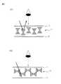
図1は、コレステリック液晶の状態を説明する図である。図1の(A)および(B)に示すように、コレステリック液晶を利用した表示素子10は、上側基板11と、コレステリック液晶層12と、下側基板13と、有する。コレステリック液晶には、図1の(A)に示すように入射光を反射するプレーナ状態と、図1の(B)に示すように入射光を反射するフォーカルコニック状態と、があり、これらの状態は、無電界下でも安定してその状態が保持される。 FIG. 1 is a diagram for explaining a state of a cholesteric liquid crystal. As shown in FIGS. 1A and 1B, the
プレーナ状態の時には、液晶分子のらせんピッチに応じた波長の光を反射する。反射が最大となる波長λは、液晶の平均屈折率n、らせんピッチpから次の式で表される。 In the planar state, light having a wavelength corresponding to the helical pitch of the liquid crystal molecules is reflected. The wavelength λ at which the reflection is maximum is expressed by the following formula from the average refractive index n of the liquid crystal and the helical pitch p.
λ=n・p
一方、反射帯域△λは、液晶の屈折率異方性△nに伴って大きくなる。λ = n · p
On the other hand, the reflection band Δλ increases with the refractive index anisotropy Δn of the liquid crystal.
プレーナ状態の時には、入射光が反射するので「明」状態、すなわち白を表示することができる。一方、フォーカルコニック状態の時には、下側基板13の下に光吸収層を設けることにより、液晶層を透過した光が吸収されるので「暗」状態、すなわち黒を表示することができる。 In the planar state, incident light is reflected, so that a “bright” state, that is, white can be displayed. On the other hand, in the focal conic state, by providing a light absorption layer under the
次に、コレステリック液晶を利用した表示素子の駆動原理を説明する。 Next, the principle of driving a display element using cholesteric liquid crystal will be described.
液晶に強い電界を与えると、液晶分子のらせん構造は完全にほどけ、全ての分子が電界の向きにしたがうホメオトロピック状態になる。次に、ホメオトロピック状態から急激に電界をゼロにすると、液晶のらせん軸は電極に垂直になり、らせんピッチに応じた光を選択的に反射するプレーナ状態になる。一方、液晶分子のらせん構造が解けない程度の弱い電界の形成後の電界除去、あるいは強い電界をかけ緩やかに電界を除去した場合は、液晶のらせん軸は電極に平行になり、入射光を透過するフォーカルコニック状態になる。また、中間的な強さの電界を与え、急激に除去すると、プレーナ状態とフォーカルコニック状態が混在し、中間調の表示が可能となる。この現象を利用して情報の表示を行う。 When a strong electric field is applied to the liquid crystal, the helical structure of the liquid crystal molecules is completely unwound, and all molecules become homeotropic according to the direction of the electric field. Next, when the electric field is suddenly reduced to zero from the homeotropic state, the spiral axis of the liquid crystal becomes perpendicular to the electrode, and a planar state in which light according to the spiral pitch is selectively reflected is obtained. On the other hand, when the electric field is removed after forming a weak electric field that does not dissolve the helical structure of the liquid crystal molecules, or when the electric field is gently removed by applying a strong electric field, the liquid crystal's helical axis is parallel to the electrode and transmits incident light. It becomes a focal conic state. Further, when an electric field having an intermediate strength is applied and removed rapidly, a planar state and a focal conic state are mixed, and halftone display is possible. Information is displayed using this phenomenon.
コレステリック液晶を利用した表示素子に画像を表示する場合に用いられる駆動方法には、多くの方法が提案されているが、「コンベンショナル駆動方法」と「ダイナミック駆動方法」の2つに大別できる。ダイナミック駆動方法は、上記の「ホメオトロピック状態」、「プレーナ状態」および「フォーカルコニック状態」に加えて、トランジェントプレーナ状態を用いる。ダイナミック駆動方法は、表示を比較的高速で書換えることができるが、精密な階調制御が難しいという問題があった。これに対して、コンベンショナル駆動方法は、精密な階調制御による高画質表示が可能であるが、表示の書換えに長時間を要するという問題があった。ここでは、コレステリック液晶を利用した表示素子をコンベンショナル駆動方法で駆動する場合を例として説明する。 Many methods have been proposed as driving methods used when displaying an image on a display element using cholesteric liquid crystal, and can be broadly classified into two methods, “conventional driving method” and “dynamic driving method”. The dynamic driving method uses a transient planar state in addition to the above-mentioned “homeotropic state”, “planar state”, and “focal conic state”. The dynamic driving method can rewrite the display at a relatively high speed, but has a problem that precise gradation control is difficult. On the other hand, the conventional driving method enables high-quality display by precise gradation control, but has a problem that it takes a long time to rewrite the display. Here, a case where a display element using cholesteric liquid crystal is driven by a conventional driving method will be described as an example.
コンベンショナル駆動方法では、全画素に高電圧を印加してホメオトロピック状態にした後、電界を解除して、全画素をプレーナ状態またはフォーカルコニック状態にするリセット動作を行う。その後、単純マトリクス駆動方法で、比較的低い電圧の短いパルス幅の書込みパルスを印加して、プレーナ状態またはフォーカルコニック状態から、画素ごとに状態を変化させる書込み動作を行う。ここでは、リセット動作で全画素をプレーナ状態にした後、書込み動作で、プレーナ状態を維持するか、フォーカルコニック状態またはプレーナ状態とフォーカルコニック状態の混在した状態に変化させる場合を例として説明する。 In the conventional driving method, after applying a high voltage to all the pixels to bring them into a homeotropic state, the electric field is released, and a reset operation is performed to bring all the pixels into a planar state or a focal conic state. Thereafter, a write operation for changing the state of each pixel from the planar state or the focal conic state is performed by applying a write pulse having a relatively low voltage and a short pulse width by a simple matrix driving method. Here, a case will be described as an example in which all the pixels are brought into the planar state by the reset operation, and then the planar state is maintained by the write operation, or the state is changed to the focal conic state or the mixed state of the planar state and the focal conic state.
図2は、コンベンショナル駆動方法において、液晶セル(画素)に印加される電圧波形の例、および図示の電圧波形を印加した場合の反射率の応答特性の例を示す図である。図2の(A)は、リセット動作において印加するリセット電圧波形(パルス)を示しており、図32(B)は、リセットパルスの印加に対する応答を示している。図2の(C)は、書込み動作において印加する書込み電圧波形(パルス)の一例を示しており、図2の(D)は、初期状態がプレーナ状態の場合の図2の(C)の書込みパルスの印加に対する応答を示している。また、図2の(E)は、図2の(C)より狭いパルス幅の書込みパルスを示しており、図2の(F)は、初期状態がプレーナ状態の場合の図2の(E)の書込みパルスの印加に対する応答を示している。言い換えれば、図2の(D)および(F)は、図2の(B)のPで示す左側の傾斜部における変化を示している。 FIG. 2 is a diagram illustrating an example of a voltage waveform applied to a liquid crystal cell (pixel) and an example of a response characteristic of reflectance when the illustrated voltage waveform is applied in the conventional driving method. 2A shows a reset voltage waveform (pulse) applied in the reset operation, and FIG. 32B shows a response to the application of the reset pulse. FIG. 2C shows an example of a write voltage waveform (pulse) applied in the write operation, and FIG. 2D shows the write of FIG. 2C when the initial state is the planar state. The response to the application of a pulse is shown. 2E shows a write pulse having a narrower pulse width than that of FIG. 2C. FIG. 2F shows the case of FIG. 2E when the initial state is the planar state. The response to the application of the write pulse is shown. In other words, (D) and (F) of FIG. 2 show changes in the left inclined portion indicated by P in (B) of FIG.
コレステリック液晶の駆動波形は、一般の液晶と同様に、液晶材料の劣化(分極)を抑制するために交流とする必要がある。このため、液晶ドライバIC(一般にコレステリック液晶専用IC、またはSTN液晶用ICが用いられる)は液晶セルに印加される電界の極性を反転させる機能を有しており、液晶駆動用の高圧電源は+数十Vの単一電源が使用できる。 The driving waveform of the cholesteric liquid crystal needs to be an alternating current in order to suppress the deterioration (polarization) of the liquid crystal material, as in a general liquid crystal. Therefore, a liquid crystal driver IC (generally a cholesteric liquid crystal dedicated IC or an STN liquid crystal IC is used) has a function of inverting the polarity of an electric field applied to a liquid crystal cell, and a high voltage power source for driving a liquid crystal is + A single power supply of several tens of volts can be used.
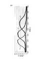
まず、図2の(A)に示すような正負のパルスを合わせたパルス幅が60msと広いパルスを印加する場合で、パルス電圧を0Vから徐々に上げていった場合の状態変化について述べる。初期状態がプレーナ状態の場合、状態は図2の(B)においてPで示す線に沿って変化する。パルス電圧がある電圧を超えると徐々にフォーカルコニック状態に遷移し、反射率は急激に低下する。反射率が最小値に達すると、パルス電圧がある電圧を超えない限り反射率はほとんど変化しない。パルス電圧がある電圧を超えると徐々にプレーナ状態に遷移し、反射率は急激に上昇する。反射率が最大値に達すると,パルス電圧を上げても反射率は変化しない。このような電圧−反射率特性は、一般に「VR特性」と呼ばれる。初期状態がフォーカルコニック状態の場合、状態は図2の(B)においてFCで示す線に沿って変化する。パルス電圧がある電圧を超えない限り反射率は変化しない。パルス電圧がある電圧を超えると徐々にプレーナ状態に遷移し、反射率は急激に上昇する。反射率が最大値に達すると、パルス電圧を上げても反射率は変化しない。そして、初期状態がプレーナ状態であってもフォーカルコニック状態であっても、ある電圧以上の電圧を印加すると、必ず反射率が最大値のプレーナ状態になる。図2の(B)では、パルス幅60msで電圧が±36Vのパルスの場合、必ずプレーナ状態になるので、このパルスをリセットパルスとして使用することができる。 First, the state change when the pulse voltage is gradually increased from 0 V in the case of applying a pulse having a wide pulse width of 60 ms including positive and negative pulses as shown in FIG. When the initial state is the planar state, the state changes along a line indicated by P in FIG. When the pulse voltage exceeds a certain voltage, the state gradually changes to the focal conic state, and the reflectivity rapidly decreases. When the reflectance reaches a minimum value, the reflectance hardly changes unless the pulse voltage exceeds a certain voltage. When the pulse voltage exceeds a certain voltage, the state gradually changes to the planar state, and the reflectance increases rapidly. When the reflectance reaches the maximum value, the reflectance does not change even if the pulse voltage is increased. Such voltage-reflectance characteristics are generally called “VR characteristics”. When the initial state is the focal conic state, the state changes along the line indicated by FC in FIG. The reflectivity does not change unless the pulse voltage exceeds a certain voltage. When the pulse voltage exceeds a certain voltage, the state gradually changes to the planar state, and the reflectance increases rapidly. When the reflectance reaches the maximum value, the reflectance does not change even if the pulse voltage is increased. Whether the initial state is the planar state or the focal conic state, when a voltage higher than a certain voltage is applied, the planar state with the maximum reflectance is always obtained. In FIG. 2B, in the case of a pulse having a pulse width of 60 ms and a voltage of ± 36 V, a planar state is always obtained, so that this pulse can be used as a reset pulse.
これよりもパルス幅が狭いパルスを印加する場合、応答性はシフトする。たとえば、図2の(C)に示すパルス幅が2msで、パルス電圧が±24Vと±12Vのパルスを印加する場合、初期状態がプレーナ状態であれば、状態は図2の(D)においてLで示す線に沿って変化する。図2の(D)においては、±12Vのパルスでは反射率は変化せず、プレーナ状態が維持される。±24Vのパルスでは反射率が少し低下した中間調となる。また、初期状態がプレーナ状態とフォーカルコニック状態が混在した反射率が中間値の場合は、状態は図2の(D)においてMで示す線に沿って変化する。この場合も、±12Vのパルスでは反射率は変化せず、±24Vのパルスでは反射率が少し低下する。 When applying a pulse having a narrower pulse width than this, the response is shifted. For example, when a pulse with a pulse width of 2 ms and a pulse voltage of ± 24 V and ± 12 V shown in FIG. 2C is applied and the initial state is the planar state, the state is L in FIG. It changes along the line indicated by. In FIG. 2D, the reflectivity does not change with a pulse of ± 12 V, and the planar state is maintained. With a pulse of ± 24 V, the halftone with a slightly reduced reflectivity is obtained. When the reflectivity in which the initial state is a mixture of the planar state and the focal conic state is an intermediate value, the state changes along a line indicated by M in FIG. Also in this case, the reflectivity does not change with a pulse of ± 12 V, and the reflectivity slightly decreases with a pulse of ± 24 V.
さらに、図2の(E)に示すパルス幅が1msで、パルス電圧が±24Vと±12Vのパルスを印加する場合、初期状態がプレーナ状態であれば、状態は図2の(F)においてNで示す線に沿って変化する。図2の(F)においては、±12Vのパルスでは反射率は変化せず、プレーナ状態が維持される。±24Vのパルスでは反射率が少し低下した中間調となるが、反射率の低下量は、2msのパルス幅の場合より小さい。すなわち、2msの方が1msより暗い階調となる。初期状態がプレーナ状態とフォーカルコニック状態が混在した反射率が中間値の場合は、状態は図2の(F)においてOで示す線に沿って変化する。この場合も、±12Vのパルスでは反射率は変化せず、±24Vのパルスでは反射率が少し低下する。 Further, when a pulse with a pulse width of 1 ms and a pulse voltage of ± 24 V and ± 12 V shown in FIG. 2E is applied and the initial state is a planar state, the state is N in FIG. It changes along the line indicated by. In FIG. 2F, the reflectivity does not change with a pulse of ± 12 V, and the planar state is maintained. In the case of a pulse of ± 24 V, the halftone with a slight decrease in reflectivity is obtained, but the decrease in reflectivity is smaller than that in the case of a pulse width of 2 ms. That is, 2 ms is darker than 1 ms. When the reflectivity in which the initial state is a mixture of the planar state and the focal conic state is an intermediate value, the state changes along a line indicated by O in FIG. Also in this case, the reflectivity does not change with a pulse of ± 12 V, and the reflectivity slightly decreases with a pulse of ± 24 V.
以上のように、初期状態がプレーナ状態の場合、比較的小さな電圧の短いパルスを印加すると、反射率が低下し、反射率の低下量は、パルス電圧およびパルス幅に応じて変化することが分かる。具体的には、パルス電圧が高いほど、パルス幅が大きいほど、反射率の低下量は大きくなる。また、図2の(D)および(F)のMおよびOで示す変化から、パルスを分けて印加しても同様の変化が起き、反射率の低下量はパルス幅の合計、すなわち累積パルス印加時間に関係する。 As described above, when the initial state is the planar state, it is understood that when a short pulse with a relatively small voltage is applied, the reflectivity is decreased, and the amount of decrease in reflectivity changes according to the pulse voltage and the pulse width. . Specifically, the lower the pulse voltage, the larger the pulse width, the greater the amount of decrease in reflectance. In addition, from the changes indicated by M and O in (D) and (F) of FIG. 2, the same change occurs even when the pulses are applied separately, and the amount of decrease in reflectance is the sum of the pulse widths, that is, cumulative pulse application Related to time.
以上の説明は、初期状態がプレーナ状態の場合で、図2の(B)において、Pで示す左側の傾斜部分を利用した例であるが、初期状態がフォーカルコニック状態の場合で、図2の(B)において、FCで示す右側の傾斜部分を利用する場合も同様である。 The above description is an example in which the initial state is the planar state and the left inclined portion indicated by P in FIG. 2B is used. However, the initial state is the focal conic state, and FIG. The same applies to the case where the right inclined portion indicated by FC is used in (B).
さらに、コンベンショナル駆動方法においても、各種の駆動方法が提案されているが、ここでは詳細な説明は省略する。 Further, various driving methods have been proposed in the conventional driving method, but detailed description thereof is omitted here.
以上説明したように、各種の駆動方法があるが、それぞれ長所・短所があり、用途に応じて適宜選択されるべきものである。以下に説明する実施形態のコレステリック液晶を利用した表示素子は、上記のいずれの駆動方法も適用可能である。 As described above, there are various driving methods, but each has advantages and disadvantages, and should be appropriately selected according to the application. Any of the above driving methods can be applied to the display element using the cholesteric liquid crystal according to the embodiment described below.
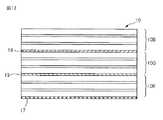
図3は、3層のコレステリック液晶層を積層した反射型カラー表示素子の概略断面図である。 FIG. 3 is a schematic cross-sectional view of a reflective color display element in which three cholesteric liquid crystal layers are laminated.
図3に示すように、表示素子10は、見る側から順番に、青(ブルー)用パネル10B、緑(グリーン)用パネル10G、および赤(レッド)用パネル10Rの3枚のパネルが積層されており、レッド用パネル10Rの下側には光吸収層17が設けられている。パネル10B、10Gおよび10Rは、同じ構成を有するが、パネル10Bは反射の中心波長が青色、パネル10Gは反射の中心波長が緑色、パネル10Rは反射の中心波長が赤色になるように、液晶材料およびカイラル材が選択され、カイラル材の含有率が決定されている。積層された3枚のパネルには、それぞれ画素が形成され、反射型カラー表示素子の画素は、積層された3枚のパネルの画素を含む。各パネルの画素は、それぞれ所定の反射色を呈するので、ここでは各パネルの画素を色相要素と称し、3枚のパネルの色相要素を第1色相要素、第2色相要素および第3色相要素と称する場合がある。各色相要素が呈する反射スペクトルの中心波長は、第1色相要素<第2色相要素<第3色相要素の順であるとする。したがって、図3の例では、第1色相要素がパネル10Bの画素に、第2色相要素がパネル10Gの画素に、第3色相要素がパネル10Rの画素に、それぞれ対応する。 As shown in FIG. 3, the
図4は、図3の反射型カラー表示素子で使用されている各層の、プレーナ状態における分光反射特性の代表例を示す図である。図4において、B、GおよびRが、青色層10B、緑色層10Gおよび赤色層10Rの反射スペクトルを示す。図4において、各層の分光反射特性はそれぞれ正規分布に近い特性を有しており、青色層10Bは反射中心波長が約480nmであり、緑色層10Gは反射中心波長が約550nmであり、赤色層10Rは反射中心波長が約630nmである。 FIG. 4 is a diagram showing a representative example of spectral reflection characteristics in the planar state of each layer used in the reflective color display element of FIG. In FIG. 4, B, G, and R indicate the reflection spectra of the
上記のように、これまでの代表例のコレステリック液晶素子の反射スペクトルは、少しでも明るさを上げるため、標準RGBに比べて、緑色(Green:G)層の反射中心波長は、視感度がピークを示す555nm(黄緑)付近に配していた。また、青色(Blue:B)層および赤色(Red:R)層の反射中心波長は、緑色層の波長に近づけて、グレーバランスを保っていた。そのため、ある程の明るさが得られる一方で、3色が緑色に偏っているため、色再現範囲が狭かった。 As described above, the reflection spectrum of the cholesteric liquid crystal element of the typical example so far increases the brightness even a little, so the reflection center wavelength of the green (Green: G) layer has a peak visibility compared to standard RGB. It was arranged in the vicinity of 555 nm (yellowish green). Further, the reflection center wavelengths of the blue (Blue: B) layer and the red (Red: R) layer were close to the wavelength of the green layer, and the gray balance was maintained. Therefore, while a certain level of brightness can be obtained, the color reproduction range is narrow because the three colors are biased to green.
また、通常、液晶組成物には同一の原材料(ネマティック液晶やカイラル材)を用いるため、λ=n・p(n:液晶の平均屈折率、p:らせんピッチ)の関係から、半値幅(△λ)は、△λ=△n・pとなり、赤色>緑色>青色の大小関係が一般的だった。しかしながら、この半値幅がこのような関係を有する場合、青色の彩度が高すぎ、一方で赤色の彩度が低くなりすぎる傾向があり、RGBのカラーバランスを好適に保てなかった。 In general, since the same raw material (nematic liquid crystal or chiral material) is used for the liquid crystal composition, the half-value width (Δ) from the relationship of λ = n · p (n: average refractive index of liquid crystal, p: helical pitch) λ) is Δλ = Δn · p, and the general relationship of red> green> blue is common. However, when the half width has such a relationship, the saturation of blue tends to be too high, while the saturation of red tends to be too low, and the RGB color balance cannot be suitably maintained.
上記の例のほかに、RGBの3層のうち赤色層における分光反射特性の半値幅を狭くすることにより、赤色の彩度を向上させることが提案されている。このような特性は、コレステリック液晶のホストとなるネマティック液晶の屈折率異方性(△n)を、RGBの3層のうち赤色層において最小にするか、あるいは添加するカイラル剤の螺旋ねじれ力を、赤色層において最小にすることにより実現される。 In addition to the above example, it has been proposed to improve the red saturation by narrowing the half-value width of the spectral reflection characteristics in the red layer of the three RGB layers. Such characteristics minimize the refractive index anisotropy (Δn) of the nematic liquid crystal that is the host of the cholesteric liquid crystal in the red layer of the three RGB layers, or reduce the helical twisting force of the added chiral agent. This is achieved by minimizing in the red layer.
しかし、赤色層における分光反射特性の半値幅△λを、緑色層および青色層の半値幅よりも小さくするだけでは、色再現範囲を十分に向上させることができないことが分かった。 However, it has been found that the color reproduction range cannot be sufficiently improved only by making the half-value width Δλ of the spectral reflection characteristic in the red layer smaller than the half-value width of the green layer and the blue layer.
他に、コレステリック液晶を利用する反射型カラー表示素子ではなく、バックライトを利用する透過型液晶表示素子では、カラーフィルタの特性を、バックライトの分光特性、例えばLEDの発光特性に応じた特性にすることが提案されている。しかし、これらの特性は、コレステリック液晶を利用する反射型カラー表示素子には適用できない。 In addition, in a transmissive liquid crystal display element using a backlight instead of a reflective color display element using cholesteric liquid crystal, the characteristics of the color filter are changed according to the spectral characteristics of the backlight, for example, the light emission characteristics of the LED. It has been proposed to do. However, these characteristics cannot be applied to a reflective color display element using cholesteric liquid crystal.
以上のように、ほかに類のない正規分布に近似した反射特性を有するコレステリック液晶層を利用する反射型カラー液晶表示素子で、最大の色再現範囲を実現することについては、これまで検討されていなかった。以下に説明するコレステリック液晶層を利用する反射型カラー表示素子によれば、色再現範囲が拡大され、カラー表示の鮮やかさなどの色表示の品質が向上する。 As described above, a reflective color liquid crystal display element using a cholesteric liquid crystal layer having a reflection characteristic approximating a normal distribution that is unparalleled has been studied to realize the maximum color reproduction range. There wasn't. According to the reflective color display element using the cholesteric liquid crystal layer described below, the color reproduction range is expanded, and the quality of color display such as vividness of color display is improved.
実施形態を説明する前に、説明で使用する色の名称と波長スペクトルとの関係を説明する。 Before describing the embodiment, the relationship between the name of the color used in the description and the wavelength spectrum will be described.
図5は、波長スペクトルと色名の関係を示す図であり、色は日本名および対応する英語名を示し、表示する記号も合わせて示す。波長スペクトルが380〜430nmの色名は「青みの紫(bluish Purple)」である。波長スペクトルが430〜467nmの色名は「紫みの青(purplish Blue)」である。波長スペクトルが467〜483nmの色名は「青(Blue)」である。波長スペクトルが483〜488nmの色名は「緑みの青(greenish Blue)」である。波長スペクトルが488〜493nmの色名は「青緑(Blue Green)」である。波長スペクトルが493〜498nmの色名は「青みの緑(bluish Green)」である。波長スペクトルが498〜530nmの色名は「緑(Green)」である。波長スペクトルが498〜530nmの色名は「緑(Green)」である。波長スペクトルが530〜558nmの色名は「黄みの緑(yellowish Green)」である。波長スペクトルが558〜569nmの色名は「黄緑(Yellow Green)」である。波長スペクトルが569〜573nmの色名は「緑みの黄(greenish Yellow)」である。波長スペクトルが573〜578nmの色名は「黄(Yellow)」である。波長スペクトルが578〜586nmの色名は「黄みの黄赤(yellowish Orange)」である。波長スペクトルが586〜597nmの色名は「黄赤(Orange)」である。波長スペクトルが597〜640nmの色名は「赤みの黄赤(reddish Orange)」である。波長スペクトルが640〜780nmの色名は「赤(Red)」である。また、後述する図12に示すように、ピンク(Pink)、黄赤ピンク(Orange Pink)などの色名も使用される。 FIG. 5 is a diagram showing the relationship between the wavelength spectrum and the color name. The color indicates the Japanese name and the corresponding English name, and the symbols to be displayed are also shown. The color name having a wavelength spectrum of 380 to 430 nm is “bluish purple”. The color name having a wavelength spectrum of 430 to 467 nm is “purplish blue”. The color name having a wavelength spectrum of 467 to 483 nm is “Blue”. The color name having a wavelength spectrum of 483 to 488 nm is “greenish blue”. The color name having a wavelength spectrum of 488 to 493 nm is “Blue Green”. The color name having a wavelength spectrum of 493 to 498 nm is “bluish green”. The color name having a wavelength spectrum of 498 to 530 nm is “Green”. The color name having a wavelength spectrum of 498 to 530 nm is “Green”. The color name having a wavelength spectrum of 530 to 558 nm is “yellowish green”. The color name having a wavelength spectrum of 558 to 569 nm is “Yellow Green”. The color name having a wavelength spectrum of 569 to 573 nm is “greenish yellow”. The color name having a wavelength spectrum of 573 to 578 nm is “Yellow”. The color name having a wavelength spectrum of 578 to 586 nm is “yellowish orange”. The color name having a wavelength spectrum of 586 to 597 nm is “Orange”. The color name having a wavelength spectrum of 597 to 640 nm is “reddish orange”. The color name having a wavelength spectrum of 640 to 780 nm is “Red”. Further, as shown in FIG. 12 to be described later, color names such as pink and yellow red pink are also used.
また、「色体積」は、色再現範囲の指標として最も適切と考えられるので、色再現範囲の大きさは色体積で表すものとする。また、ディスプレイの標準規格として、IEC(International Electrotechnical Commission)等で規格化されている標準RGB(standard RGB:sRGB)を基準にして、説明を行う。 In addition, since “color volume” is considered to be the most appropriate as an index of the color reproduction range, the size of the color reproduction range is represented by the color volume. Further, description will be made with reference to standard RGB (standard RGB: sRGB) standardized by IEC (International Electrotechnical Commission) or the like as a display standard.
まず、各液晶層の反射中心波長(以下、主波長と称する)について述べる。主波長は、各液晶層の反射色の色相に関係する。 First, the reflection center wavelength (hereinafter referred to as the main wavelength) of each liquid crystal layer will be described. The dominant wavelength is related to the hue of the reflected color of each liquid crystal layer.
コレステリック液晶を利用した通常の反射型カラー表示素子では、青色層の反射色をsRGBのBとほぼ同等、緑色層の反射色をsRGBのGと同等か長波長側にシフトした色とし、赤色層の反射色をsRGBのRとほぼ同等、としていた。しかし、コレステリック液晶のような広域スペクトルの場合、青色層および緑色層の反射色をsRGBよりも短波長化することが、明るさ・彩度のバランスの点から望ましい。なお、赤色層の反射色はsRGBのRとほぼ同等でよい。各液晶層の反射色をこのように設定することで、濃紺〜深緑といった記憶色に近い領域を再現可能とし、全体的な色再現範囲を極大化できる。 In a normal reflection type color display element using cholesteric liquid crystal, the reflection color of the blue layer is substantially the same as B of sRGB and the reflection color of the green layer is the same as G of sRGB or shifted to the longer wavelength side, and the red layer The reflection color of the sRGB is almost the same as the R of sRGB. However, in the case of a broad spectrum such as a cholesteric liquid crystal, it is desirable from the viewpoint of the balance between brightness and saturation that the reflected colors of the blue layer and the green layer be shorter than sRGB. Note that the reflection color of the red layer may be substantially the same as R of sRGB. By setting the reflection color of each liquid crystal layer in this way, it is possible to reproduce an area close to a memory color such as dark blue to dark green, and to maximize the overall color reproduction range.
次に、各液晶層の反射スペクトルの半値幅(△λ)について述べる。 Next, the half width (Δλ) of the reflection spectrum of each liquid crystal layer will be described.
sRGBは、隣接する色のスペクトルが重複しない狭域スペクトルが理想形とされている。反射型のカラー表示素子であれば、青色層と緑色層の反射スペクトルが重複せず、緑色層と赤色層の反射スペクトルが重複しないことが望ましい。しかし、コレステリック液晶層は干渉反射により反射色を呈し、液晶層の反射スペクトルは、隣接色と部分的に重複する広さを有するため、コレステリック液晶の条件は、sRGBと異なる。 sRGB has an ideal form of a narrow spectrum in which the spectra of adjacent colors do not overlap. In the case of a reflective color display element, it is desirable that the reflection spectra of the blue layer and the green layer do not overlap and the reflection spectra of the green layer and the red layer do not overlap. However, since the cholesteric liquid crystal layer exhibits a reflected color due to interference reflection, and the reflection spectrum of the liquid crystal layer has a width that partially overlaps with the adjacent color, the conditions of the cholesteric liquid crystal are different from sRGB.
前述のように、コレステリック液晶組成物には同一の原材料(ネマティック液晶やカイラル材)を用いるため、λ=n・pの関係から、各層の半値幅△λは、赤色>緑色>青色の大小関係が一般的であった。言い換えれば青色層の半値幅が最小であった。また、前述のように、赤色層の半値幅を最小にすることも提案されている。 As described above, since the same raw material (nematic liquid crystal or chiral material) is used for the cholesteric liquid crystal composition, from the relationship of λ = n · p, the half-value width Δλ of each layer is a relationship of red> green> blue. Was common. In other words, the half width of the blue layer was the smallest. As described above, it has also been proposed to minimize the half-value width of the red layer.
これに対して、実施形態では、緑色層の反射スペクトルの半値幅を最小にし、各層の半値幅△λは、赤色>青色≧緑色する。このように、これまでは、緑色層の半値幅は、青色層と赤色層の中間的な半値幅であったのに対して、実施形態では、3色の層の中で緑色層の半値幅を最小にする。これにより、更に深い緑色の再現が可能となる。 On the other hand, in the embodiment, the half-value width of the reflection spectrum of the green layer is minimized, and the half-value width Δλ of each layer satisfies red> blue ≧ green. Thus, up to now, the half-value width of the green layer was an intermediate half-value width of the blue layer and the red layer, whereas in the embodiment, the half-value width of the green layer among the three color layers. To minimize. As a result, a deeper green color can be reproduced.
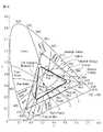
図6は、実施形態において、青色層および緑色層の反射色をsRGBよりも短波長化すると共に、緑色層の反射スペクトルの半値幅を最小にした効果を、マックアダム(McAdam)の識別域(楕円)で説明する図である。マックアダム(McAdam)の識別域(楕円)は、同じ明るさを有する二つの色刺激の、色度を見分け得る最小の差(識別域)であり、図6は、xy色度図上において識別域(楕円)を示している。 FIG. 6 shows the effect of reducing the reflection color of the blue layer and the green layer to be shorter than that of sRGB and minimizing the half-value width of the reflection spectrum of the green layer in the embodiment. FIG. McAdam's discriminating area (ellipse) is the smallest difference (identifying area) between two color stimuli having the same brightness that can distinguish the chromaticity. FIG. 6 shows the discriminating area on the xy chromaticity diagram. The area (ellipse) is shown.
図6において、Xで示す三角形は、3層の反射スペクトルが図4に示した特性を有する場合の色再現範囲を示し、Yで示す三角形の範囲は、sRGBの場合の色再現範囲を示す。短波長化は、図6において、B’、G’およびR’を、白(三角形のほぼ中心位置)に対して反時計回りに回転することに相当し、長波長化は、逆に時計回りに回転することに相当する。 In FIG. 6, a triangle indicated by X indicates a color reproduction range when the three-layer reflection spectrum has the characteristics shown in FIG. 4, and a triangle range indicated by Y indicates a color reproduction range in the case of sRGB. Shortening the wavelength corresponds to rotating B ′, G ′ and R ′ counterclockwise with respect to white (approximately the center position of the triangle) in FIG. Is equivalent to rotating.
B’を短波長化すると、識別できる色差が大きくなり、さらに半値幅を狭める狭帯域化すると、表示する色の色純度を向上できる。G’を短波長化すると共に狭帯域化すると、識別できる色差が大きくなり、表示する色の色純度を向上できる。R’は、短波長化するとRから離れてオレンジ色になり、sRGBのRより長波長化すると茶色になるので、sRGBのRと同等が望ましい。 When the wavelength of B ′ is shortened, the color difference that can be identified increases, and when the band width is narrowed to narrow the half-value width, the color purity of the displayed color can be improved. When G 'is shortened and the band is narrowed, the color difference that can be identified increases, and the color purity of the displayed color can be improved. Since R ′ becomes orange apart from R when the wavelength is shortened, and brown when the wavelength is longer than R of sRGB, R ′ is preferably equal to R of sRGB.
より詳しく説明すると、青色(B)層は、反射スペクトルが広いコレステリック液晶の場合、sRGBと同等の主波長であると、不純色成分(例えばシアン)が残存する。そのため、図6において、B’からBに、主波長を短波長側にシフトさせ、含まれていたシアン成分を減少させた。この時、短波長側にシフトすると、青色(B)の彩度が向上する一方で、明度が低下する。この明度の低下を補正するため、実施形態では、半値幅を後述の緑色(G)よりも相対的に広く、赤色(R)よりも相対的に狭くする。このようにすることで、明度の低下を最小限に抑えつつ、濃紺領域の色相が再現可能となり、この相対関係が、色体積の極大化を可能にする。言い換えれば、青色(B)は、主波長がsRGBよりも短波長で、かつ半値幅は緑色(G)よりも相対的に広く、赤色(R)よりも相対的に狭いことが,色再現範囲を最大化させる上で望ましい。具体的には、青色(B)層の反射スペクトルは、主波長が430nm〜460nmの範囲で、半値幅が75nm〜115nmの範囲であることが望ましい。 More specifically, when the blue (B) layer is a cholesteric liquid crystal having a wide reflection spectrum, an impure color component (for example, cyan) remains when the main wavelength is the same as that of sRGB. Therefore, in FIG. 6, the main wavelength is shifted from B ′ to B toward the short wavelength side, and the contained cyan component is reduced. At this time, when shifting to the short wavelength side, the saturation of blue (B) is improved while the brightness is lowered. In order to correct this decrease in brightness, in the embodiment, the half-value width is relatively wider than green (G), which will be described later, and is relatively narrower than red (R). By doing so, it is possible to reproduce the hue of the dark blue region while minimizing the decrease in lightness, and this relative relationship enables the color volume to be maximized. In other words, the color reproduction range of blue (B) is that the dominant wavelength is shorter than sRGB, the half-value width is relatively wider than green (G), and is relatively narrower than red (R). It is desirable to maximize Specifically, it is desirable that the reflection spectrum of the blue (B) layer has a dominant wavelength in the range of 430 nm to 460 nm and a half width in the range of 75 nm to 115 nm.
緑色(G)層は、反射スペクトルが広いコレステリック液晶の場合、主波長が550nm付近であると、黄色(Y)成分を多く含み、緑色の彩度は最も低く、深緑などの重要色が再現不能であった。緑色(G)の彩度を高くするために、まず主波長を短波長化して、黄色(Y)成分を低減した。この短波長化は,図6の楕円からも窺えるように、楕円の短軸側にシフトするので、視覚的に色味を劇的に改善でき、彩度が大きく向上することができる。 In the case of cholesteric liquid crystal with a wide reflection spectrum, the green (G) layer contains a large amount of yellow (Y) component when the dominant wavelength is around 550 nm, the green color is the lowest, and important colors such as deep green cannot be reproduced. Met. In order to increase the saturation of green (G), the main wavelength was first shortened to reduce the yellow (Y) component. This shortening of the wavelength shifts to the short axis side of the ellipse, as can be seen from the ellipse in FIG. 6, so that the color tone can be improved dramatically and the saturation can be greatly improved.
緑色(G)層の反射スペクトルの半値幅は、青色層とは異なり、従来よりも狭くすることが望ましい。緑色(G)層の反射スペクトルの半値幅を多少狭めて、明るさを多少犠牲にしてでも、彩度を優先した向上させたほうが、色体積の極大化に寄与する。つまり、半値幅を狭めて、彩度をより一層高めることが望ましい。 Unlike the blue layer, the half width of the reflection spectrum of the green (G) layer is preferably narrower than the conventional one. Even if the half-value width of the reflection spectrum of the green (G) layer is somewhat narrowed and the brightness is somewhat sacrificed, the improvement in which the saturation is prioritized contributes to the maximization of the color volume. In other words, it is desirable to further increase the saturation by narrowing the half width.
以上のことをまとめると、緑色(G)層の反射スペクトルは、主波長がsRGBよりも短波長で、かつ半値幅は青色(B)層および赤色(R)層よりも相対的に狭いことが、色再現範囲を最大化させる上で望ましい。具体的には、緑色(G)層の反射スペクトルは、主波長が510nm〜540nmの範囲で、半値幅が75nm〜115nmの範囲であることが望ましい。 In summary, the reflection spectrum of the green (G) layer has a dominant wavelength shorter than sRGB and a half-value width relatively narrower than that of the blue (B) layer and the red (R) layer. This is desirable for maximizing the color reproduction range. Specifically, it is desirable that the reflection spectrum of the green (G) layer has a dominant wavelength in the range of 510 nm to 540 nm and a half width in the range of 75 nm to 115 nm.
赤色(R)層の反射スペクトルの主波長は、sRGBと同等であることが望ましい。これよりも短波長化するとオレンジ〜黄色のような不純色成分が増え、長波長化するために明度が下がって茶色っぽくなるため、sRGBと同等が望ましい。 The dominant wavelength of the reflection spectrum of the red (R) layer is desirably equivalent to sRGB. If the wavelength is shorter than this, impure color components such as orange to yellow are increased, and the lightness is lowered and brownish in order to increase the wavelength.
赤色(R)層の反射スペクトルの半値幅は、一般的な例と同様に、RGBの中では最も広くすることが好ましい。もし、赤色(R)液晶層の△nを下げることで半値幅を狭くした場合には、色体積の極大点から外れ、色体積が減少する。 The full width at half maximum of the reflection spectrum of the red (R) layer is preferably the largest in RGB as in the general example. If the half width is narrowed by reducing Δn of the red (R) liquid crystal layer, the color volume deviates from the maximum point of the color volume and the color volume decreases.
以上のことをまとめると、赤色(R)層の反射スペクトルは、主波長がsRGBと概ね同等で、かつ半値幅は青色(B)層および緑色(G)層の反射スペクトルの半値幅よりも相対的に広くすることが、表示素子の色再現範囲を最大化させる上での望ましい。具体的には、赤色(R)層の反射スペクトルは、主波長が600nm〜630nmの範囲で、半値幅が95nm〜135nmの範囲であることが望ましい。 To summarize the above, the reflection spectrum of the red (R) layer has a dominant wavelength approximately equal to that of sRGB, and the half width is relative to the half width of the reflection spectra of the blue (B) layer and the green (G) layer. It is desirable to maximize the color reproduction range in order to maximize the color reproduction range of the display element. Specifically, the reflection spectrum of the red (R) layer desirably has a dominant wavelength in the range of 600 nm to 630 nm and a half width in the range of 95 nm to 135 nm.
なお、RGBの3層の反射スペクトルの半値幅の相対関係は、RGBのうち最も小さいものに対して、それより大きいものは1.5〜1.9倍の範囲であることが望ましい。 In addition, it is desirable that the relative relationship of the half value width of the reflection spectrum of the three layers of RGB is in the range of 1.5 to 1.9 times larger than that of the smallest RGB.
主波長および半値幅の要件は以上の通りであるが、これを液晶材料の屈折率異方性(△n)に換算すると、青色(B)層の△nを3層の中で最大とし、緑色(G)層と赤色(R)層の△nをほぼ等しくすることが望ましい。言い換えれば、次のような関係を有することが望ましい。 The requirements for the dominant wavelength and the half-value width are as described above. When this is converted into the refractive index anisotropy (Δn) of the liquid crystal material, Δn of the blue (B) layer is maximized among the three layers, It is desirable to make Δn of the green (G) layer and the red (R) layer substantially equal. In other words, it is desirable to have the following relationship.
青色(B)層の△n>緑色(G)層の△n≒赤色(R)層の△n
ちなみに、これまでの一般的な例では、次のような関係であった。Δn of blue (B) layer> Δn of green (G) layer≈Δn of red (R) layer
By the way, in the general examples so far, the relationship is as follows.
青色(B)層の△n=緑色(G)層の△n=赤色(R)層の△n
具体的には、3層の△nは0.18〜0.25の範囲で、緑色(G)層と赤色(R)層の△nはそれぞれ他方の±10%以内の範囲であり、青色(B)層の△nは緑色(G)層または赤色(R)層の△nの110〜130%であることが望ましい。Δn of blue (B) layer = Δn of green (G) layer = Δn of red (R) layer
Specifically, Δn of the three layers is in the range of 0.18 to 0.25, Δn of the green (G) layer and the red (R) layer is within ± 10% of the other, and blue Δn of the (B) layer is preferably 110 to 130% of Δn of the green (G) layer or the red (R) layer.
さらに、各層の反射スペクトルのピーク値は、RGBの3層間で極端に異なるよりも、RGBの3層のうち最も低いものに対して、それより高いものは1.0〜1.5倍の範囲にあることが望ましく、色再現範囲を保持する上で重要である。 Further, the peak value of the reflection spectrum of each layer is 1.0 to 1.5 times higher than the lowest of the three layers of RGB, rather than extremely different between the three layers of RGB. It is desirable to maintain the color reproduction range.
さらに、観察面側から青色(B)層、緑色(G)層、赤色(R)層の順に積層する場合、青色(B)層と緑色(G)層の間に青色カットフィルタを、緑色(G)層と赤色(R)層の間に緑色カットフィルタを設けると、より一層の彩度向上が図れる。青色カットフィルタと緑色カットフィルタは、一方のみを設けても効果がある。 Furthermore, when laminating a blue (B) layer, a green (G) layer, and a red (R) layer in this order from the observation surface side, a blue cut filter is inserted between the blue (B) layer and the green (G) layer. If a green cut filter is provided between the G) layer and the red (R) layer, the saturation can be further improved. Even if only one of the blue cut filter and the green cut filter is provided, it is effective.
ここで、コレステリック液晶を利用したこれまでの代表的例の反射型カラー表示素子と実施形態の反射型カラー表示素子の色再現範囲を、色体積を使用して比較する。この比較は、観察面側から青色(B)層、緑色(G)層、赤色(R)層の順に積層した反射型カラー表示素子で行った。この反射型カラー表示素子は、緑色(G)層と赤色(R)層の間に緑色カットフィルタを設けて、赤色の彩度をより強調している。測定は、屋外相当の照度下で行った。 Here, the color reproduction range of the reflective color display element of the typical example using the cholesteric liquid crystal and the reflective color display element of the embodiment will be compared using the color volume. This comparison was performed using a reflective color display element in which a blue (B) layer, a green (G) layer, and a red (R) layer were laminated in this order from the observation surface side. In this reflective color display element, a green cut filter is provided between a green (G) layer and a red (R) layer to further emphasize red saturation. The measurement was performed under illuminance equivalent to the outdoors.
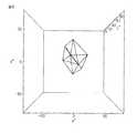
図7は、コレステリック液晶を利用した代表例の反射型カラー表示素子の反射スペクトルを示す図である。また、図8は、コレステリック液晶を利用した代表例の反射型カラー表示素子のCIELAB色空間での色体積を示す図である。色体積は、表示において色再現できる範囲を示す。 FIG. 7 is a diagram showing a reflection spectrum of a representative reflective color display element using a cholesteric liquid crystal. FIG. 8 is a diagram showing the color volume in the CIELAB color space of a representative reflective color display element using cholesteric liquid crystal. The color volume indicates a range in which colors can be reproduced in the display.
図9は、コレステリック液晶を利用した実施形態の反射型カラー表示素子の反射スペクトルを示す図である。また、図10は、コレステリック液晶を利用した実施形態の反射型カラー表示素子のCIELAB色空間での色体積を示す図である。 FIG. 9 is a diagram showing a reflection spectrum of the reflective color display element of the embodiment using cholesteric liquid crystal. FIG. 10 is a diagram showing the color volume in the CIELAB color space of the reflective color display element of the embodiment using cholesteric liquid crystal.
図7に示すように、明るさを最優先とした代表例の反射型カラー表示素子の反射スペクトルの構成では、色体積は20116(相対値)であった。また、図8に示すように、代表例の色再現範囲では、濃紺〜深緑、紫色などの再現能力が低いことが分かる。 As shown in FIG. 7, in the configuration of the reflection spectrum of the reflection type color display element of the representative example in which brightness is given the highest priority, the color volume is 20116 (relative value). Further, as shown in FIG. 8, it can be seen that in the color reproduction range of the representative example, the reproduction ability of dark blue to dark green, purple, etc. is low.
これに対して、図9に示すように、実施形態の反射型カラー表示素子の反射スペクトルの構成では、色体積は30118(相対値)であり、色体積は図7の反射スペクトルの場合に比べて約1.5倍に増加する。また、図10に示すように、実施形態の反射型カラー表示素子の色再現範囲では、濃紺〜深緑,紫色などの再現能力が向上し、代表色とされるマクベスチャートをカバーする色数も増加し、赤〜マゼンタの彩度も増している。 On the other hand, as shown in FIG. 9, in the configuration of the reflection spectrum of the reflective color display element of the embodiment, the color volume is 30118 (relative value), and the color volume is compared with the reflection spectrum of FIG. About 1.5 times. Further, as shown in FIG. 10, in the color reproduction range of the reflective color display element of the embodiment, the reproduction ability of dark blue to dark green, purple, etc. is improved, and the number of colors covering the Macbeth chart which is a representative color is increased. However, the saturation of red to magenta is also increasing.
図11は、表示素子における積層順、カットフィルタの有/無、および観察する環境条件が屋外であるか室内であるかのパラメータを変化させた時の、色体積が極大となる各層の主波長および半値幅の最適値を求めた結果を示す。明るさは、30がこれまでの表示素子のレベルであり、60が新聞に匹敵するレベルである。第1、第2および第3要素は、主波長が短い側から順に並べた3つの層に対応し、具体的には、第1要素は青色(B)層に、第2要素は緑色(G)層に、第3要素は赤色(R)層に、それぞれ対応する。 FIG. 11 shows the main wavelength of each layer in which the color volume becomes maximum when the stacking order in the display element, the presence / absence of a cut filter, and the parameters of whether the observed environmental conditions are outdoor or indoor are changed. And the result of having calculated | required the optimum value of a half value width is shown. As for the brightness, 30 is the level of the conventional display element, and 60 is a level comparable to a newspaper. The first, second, and third elements correspond to three layers arranged in order from the side with the shorter dominant wavelength. Specifically, the first element is in the blue (B) layer, and the second element is in green (G ) Layer and the third element corresponds to the red (R) layer.
色体積が極大となる条件は、これらのパラメータに依存せず、表示素子の各層の主波長および半値幅のロバスト性が高く安定していることが分かる。このように表示素子の各層の主波長および半値幅のロバスト性が高いので、これらの要件は、積層構造のみならず、RGB画素の並置構造の場合も有効であると考えられる。 It can be seen that the condition that the color volume is maximized does not depend on these parameters, and the robustness of the main wavelength and the half-value width of each layer of the display element is high and stable. Since the main wavelength and the half-value width of each layer of the display element are thus robust, these requirements are considered to be effective not only in the laminated structure but also in the RGB pixel juxtaposition structure.
図12は、CIEXYZ表色系におけるxy色度図上でのこれまでの代表例の表示素子と実施形態の表示素子の色再現範囲の比較を示す図である。図12において、Xはこれまでの代表例の表示素子の色再現範囲を、YはsRGBを、Zは実施形態の表示素子の色再現範囲を示す。図12は、図5の色名称に対応する範囲も合わせて示している。 FIG. 12 is a diagram showing a comparison of the color reproduction range of the display element of the representative example so far and the display element of the embodiment on the xy chromaticity diagram in the CIEXYZ color system. In FIG. 12, X represents the color reproduction range of the display element of the representative example so far, Y represents sRGB, and Z represents the color reproduction range of the display element of the embodiment. FIG. 12 also shows a range corresponding to the color name of FIG.
実施形態の表示素子の色再現範囲の方が、これまでの代表例の表示素子の色再現範囲よりも、xy色度図上の三角形の面積が大きく、色再現範囲が拡大している。 The color reproduction range of the display element of the embodiment has a larger area of the triangle on the xy chromaticity diagram than the color reproduction range of the display element of the representative example so far, and the color reproduction range is expanded.
図12から、青色(B)層は紫みの青(Purplish Blue)、緑色(G)層は緑(Green)もしくは黄緑(Yellowish Green)、赤色(R)層は黄赤ピンク(Orange Pink)もしくは赤みの黄赤(Reddish Orange)の色領域内に配することが望ましい。 From FIG. 12, the blue (B) layer is purple blue, the green (G) layer is green or yellow green, and the red (R) layer is orange pink. Alternatively, it is desirable to arrange in the reddish orange color region.
以上、実施形態の3つの液晶層の色特性について説明した。次に、上記で説明した色特性を実現するコレステリック液晶を利用した実施形態の反射型カラー表示素子を説明する。 The color characteristics of the three liquid crystal layers of the embodiment have been described above. Next, a reflective color display element according to an embodiment using a cholesteric liquid crystal that realizes the color characteristics described above will be described.
図13は、コレステリック液晶を利用した実施形態の単純マトリクス型の反射型カラー表示素子10の構成を示す図である。図13に示すように、表示素子10は、見る側から順番に、青色(B)パネル10B、緑色(G)10G、および赤色(R)パネル10Rの3枚のパネルが積層されており、赤色パネル10Rの下側には光吸収層17が設けられている。また、青色パネル10Bと緑色10Gの間にはブルーカットフィルタ層18が、緑色パネル10Gと赤色10Rの間にはグリーンカットフィルタ層19が、それぞれ形成されている。ブルーカットフィルタ層18は青色を吸収し、グリーンカットフィルタ層19は緑色を吸収する。 FIG. 13 is a diagram showing a configuration of a simple matrix type reflective
パネル10Bは反射の中心波長が青色付近、パネル10Gは反射の中心波長が緑色付近、パネル10Rは反射の中心波長が赤色付近になるように、液晶材料およびカイラル材が選択され、カイラル材の含有率が決定されている。パネル10B、10Gおよび10Rのコモン電極およびセグメント電極は、スキャンドライバ28およびセグメントドライバ29により駆動される。 The liquid crystal material and the chiral material are selected such that the
パネル10B、10Gおよび10Rは、反射の中心波長が異なる以外同じ構成を有する。以下、パネル10B、10Gおよび10Rの代表例を、パネル10Aとして表し、その構成を説明する。
図14は、1枚のパネル10Aの基本構成を示す図である。 FIG. 14 is a diagram showing a basic configuration of one
図14に示すように、表示素子10Aは、上側基板11と、上側基板11の表面に設けられた上側電極層14と、下側基板13の表面に設けられた下側電極層15と、シール材16と、を有する。上側基板11と下側基板13は、電極が対向するように配置され、間にコレステリック液晶材料を封入した後シール材16で封止される。なお、液晶層12内にスペーサが配置され、上側電極層14と下側電極層15の一方に複数のコモン電極が、他方に複数のセグメント電極が形成されるが、図示は省略している。複数のコモン電極および複数のセグメント電極は、互いに平行な帯状の透明電極であり、観察面から見た時に直交するように配置される。複数のコモン電極および複数のセグメント電極には、コモンドライバおよびセグメントドライバから電圧パルス信号が印加され、それにより液晶層に電圧が印加される。液晶層に電圧を印加して、液晶層の液晶分子をプレーナ状態またはフォーカルコニック状態にして表示を行う。 As shown in FIG. 14, the
上側基板11および下側基板13は、いずれも透光性を有しているが、積層の最下層のパネルの下側基板は、非透光性でもよい。透光性を有する基板としては、ガラス基板、PETまたはPCフィルム基板を使用することができる。 The
上側電極および下側電極は、例えば、ITO(インジウム錫酸化物:Indium Tin Oxide)の透明導電膜が代表的であるが、その他IZO(インジウム亜鉛酸化物:Indium Zic Oxide)等の透明導電膜などを用いることができる。 For example, the upper electrode and the lower electrode are typically transparent conductive films made of ITO (Indium Tin Oxide), but other transparent conductive films made of IZO (Indium Zic Oxide), etc. Can be used.
電極上には絶縁性のある薄膜が形成される。この絶縁性薄膜が厚いと、駆動電圧が上昇し、汎用STNドライバが使用できなくなる。逆に、絶縁性薄膜がないとリーク電流が流れてしまうため、消費電力が増大する。絶縁性薄膜は、比誘電率が5前後であり、液晶よりもかなり低いため、厚みは概ね0.3μm以下が望ましい。 An insulating thin film is formed on the electrode. If this insulating thin film is thick, the drive voltage rises and the general-purpose STN driver cannot be used. On the other hand, if there is no insulating thin film, a leakage current flows, so that power consumption increases. The insulating thin film has a relative dielectric constant of around 5 and is considerably lower than that of the liquid crystal. Therefore, the thickness is preferably about 0.3 μm or less.
上側基板11および下側基板13の間には、基板間ギャップを均一に保持するためのスペーサが挿入される。一般に、上下基板を貼り合わせる前に、樹脂製又は無機酸化物製の球体状のスペーサを均一に散布する。また、表面に熱可塑性の樹脂がコーティングしてある固着スペーサを設けてもよい。スペーサによって形成されるセルギャップは、3μm〜6μmの範囲であることが望ましい。セルギャップがこれより小さいと、反射率が低下して暗い表示になり、高い閾値急峻性も期待できない。一方、セルギャップがこれより大きいと、高い閾値急峻性は保持できるが、駆動電圧が上昇して汎用部品による駆動が困難になる。 A spacer is inserted between the
液晶層に充填する液晶組成物は、ネマティック液晶混合物にカイラル材を10〜40wt%添加したコレステリック液晶である。ここで,カイラル材の添加量はネマティック液晶成分とカイラル材の合計量を100wt%としたときの値である。ネマティック液晶としては従来から公知の各種のものを用いることができるが、誘電率異方性(Δε)が15〜25の範囲が適正範囲である。誘電率異方性が15以下であれば、駆動電圧が全体的に高くなり、駆動回路に汎用部品の適用が困難になる。一方、誘電率異方性が25以上となると、プレーナ状態からフォーカルコニック状態に変化する印加電圧の領域が小さくなり、閾値急峻性としては下がると考えられる。更には、液晶材料自体の信頼性にも懸念が出てくる。 The liquid crystal composition filled in the liquid crystal layer is a cholesteric liquid crystal obtained by adding 10 to 40 wt% of a chiral material to a nematic liquid crystal mixture. Here, the addition amount of the chiral material is a value when the total amount of the nematic liquid crystal component and the chiral material is 100 wt%. As the nematic liquid crystal, conventionally known various liquid crystals can be used, and a dielectric anisotropy (Δε) in the range of 15 to 25 is an appropriate range. If the dielectric anisotropy is 15 or less, the driving voltage increases as a whole, making it difficult to apply general-purpose components to the driving circuit. On the other hand, when the dielectric anisotropy is 25 or more, it is considered that the region of the applied voltage that changes from the planar state to the focal conic state becomes small, and the threshold steepness decreases. Furthermore, there are concerns about the reliability of the liquid crystal material itself.
屈折率異方性(△n)は、0.18〜0.25くらいが望ましい。この範囲より小さいと、プレーナ状態の反射率が低くなり、この範囲より大きいと、フォーカルコニック状態での散乱反射が大きくなる他、粘度も高くなり、応答速度が低下する。 The refractive index anisotropy (Δn) is preferably about 0.18 to 0.25. If it is smaller than this range, the reflectivity in the planar state is lowered, and if it is larger than this range, the scattering reflection in the focal conic state is increased, the viscosity is also increased, and the response speed is lowered.
図15は、液晶層に充填される液晶組成物中のカイラル材の添加量と液晶層の反射中心波長の関係を示す図である。図15に示すように、反射中心波長は、カイラル材の添加量が増加するにしたがって、線形に低下することが分かる。 FIG. 15 is a diagram showing the relationship between the amount of chiral material added in the liquid crystal composition filled in the liquid crystal layer and the reflection center wavelength of the liquid crystal layer. As shown in FIG. 15, it can be seen that the reflection center wavelength decreases linearly as the amount of chiral material added increases.
また、図16は、屈折率異方性(△n)と反射スペクトルの半値幅の関係を示す図である。半値幅は、△nが増加するにしたがって、線形に増加することが分かる。△nは、ネマティック液晶混合物やカイラル材の種類およびその混合比で制御可能である。 FIG. 16 is a diagram showing the relationship between the refractive index anisotropy (Δn) and the half-value width of the reflection spectrum. It can be seen that the full width at half maximum increases linearly as Δn increases. Δn can be controlled by the type of nematic liquid crystal mixture or chiral material and the mixing ratio thereof.
前述のように、青色(B)層10Bでは、主波長が430〜460nmの範囲で、半値幅が75〜115nmの範囲であることが望ましい。緑色(G)層10Gでは、主波長が510〜540nmの範囲で、半値幅が75〜115nmの範囲であることが望ましい。赤色(R)層10Rでは、主波長が600〜630nmの範囲で、半値幅が95〜135nmの範囲であることが望ましい。さらに、3層の△nは0.18〜0.25の範囲で、緑色(G)層10Gと赤色(R)層10Rの△nはそれぞれ他方の±10%以内の範囲であり、青色(B)層の△nは緑色(G)層または赤色(R)層の△nの110〜130%であることが望ましい。 As described above, in the blue (B)
ネマティック液晶混合物やカイラル材の種類、カイラル材の添加量(混合比)などを適宜選択して、上記のような各液晶層の特性を実現することができる。 The characteristics of each liquid crystal layer as described above can be realized by appropriately selecting the type of nematic liquid crystal mixture, chiral material, the amount of chiral material added (mixing ratio), and the like.
上記の実施形態では、3枚のパネル10B、10Gおよび10Rを積層した3層構造の表示素子の例を示したが、前述のように、表示素子の各層の主波長および半値幅のロバスト性が高いので、RGB画素の並置構造にも適用可能である。 In the above-described embodiment, an example of a display element having a three-layer structure in which three
図17は、RGB画素の並置構造を有する表示素子の構成を示す図であり(A)が上面図、(B)が断面図である。この表示素子は、2枚の基板11および13の間に設けられた隔壁43を有する。隔壁43は、2枚の基板11と13の間の空間を、複数の帯状の領域に区切る。複数の帯状の領域は、青色液晶層12B、緑色液晶層12Gおよび赤色液晶層12Rの3つのグループに分けられ、3つのグループの領域が交互に配置される。青色液晶層12Bには、主波長が430〜460nmの範囲で、半値幅が75〜115nmの範囲である反射スペクトルを呈するコレステリック液晶が充填される。緑色液晶層12Gには、主波長が510〜540nmの範囲で、半値幅が75〜115nmの範囲である反射スペクトルを呈するコレステリック液晶が充填される。赤色液晶層12Rには、主波長が600〜630nmの範囲で、半値幅が95〜135nmの範囲である反射スペクトルを呈するコレステリック液晶が充填される。 17A and 17B are diagrams illustrating a configuration of a display element having an RGB pixel juxtaposition structure, where FIG. 17A is a top view and FIG. 17B is a cross-sectional view. This display element has a
コモン電極41は、横方向伸びる。セグメント電極42は、縦方向に伸び、各帯状領域に重なるように設けられる。コモン電極41とセグメント電極42の交差部分に画素が形成される。図17に示した表示素子では、隣接する3つの青色液晶層12B、緑色液晶層12Gおよび赤色液晶層12Rの部分の3画素が、1つの表示画素を形成し、1枚でカラー表示が可能であるが、明るさは、3層構造の場合の約1/3に減少する。 The
なお、2つの帯状領域グループを有するパネルを2枚積層し、4つの帯状領域グループグループが少なくともRGBの3種類の液晶層を有するようにした2層構造の反射型カラー表示装置も実現可能である。このような2層構造の反射型カラー表示装置の3種類の液晶層が、上記のような反射スペクトル特性を有するようにしてもよい。 It is also possible to realize a reflective color display device having a two-layer structure in which two panels having two band-shaped area groups are stacked so that the four band-shaped area groups have at least three liquid crystal layers of RGB. . Three kinds of liquid crystal layers of the reflective color display device having such a two-layer structure may have the reflection spectral characteristics as described above.
図18は、上記のコレステリック液晶を利用した実施形態の単純マトリクス型の反射型カラー表示素子10を用いた表示装置の概略構成を示すブロック図である。 FIG. 18 is a block diagram showing a schematic configuration of a display device using the simple matrix reflective
この表示装置は、表示素子10と、電源21と、昇圧部22と、電圧生成部23と、電圧安定部24と、原振クロック部25と、分周部26と、コモンドライバ27と、セグメントドライバ28と、駆動制御回路29と、を有する。 The display device includes a
表示素子10は、コレステリック液晶を利用した実施形態の単純マトリクス型の反射型カラー液晶表示素子である。 The
表示素子10の画素数はCGA(横1024画素、縦768画素)とする。表示素子10の駆動方法は、前述のコンベンショナル駆動方法であるが、ダイナミック駆動方法を適用することも可能である。 The number of pixels of the
電源21は、外部から供給される電源を受ける部分または電池などで形成され、3〜5Vの直流電源を出力する。昇圧部22は、DC−DCコンバータなどを有し、3〜5Vの電圧を液晶の駆動電圧として必要とする約40Vに昇圧する。この昇圧レギュレータは、表示素子10の負荷特性、すなわち周期一定でのコンデンサの充放電に対して変換効率の高いものが好ましい。 The
電圧生成部23は、昇圧された電圧から、リセット動作時には36Vを生成し、書込み動作時にはアナログ電圧値(0/10/17/24V付近)を生成する。リセット電圧と階調書込み電圧のスイッチングには、高耐圧のアナログスイッチを用いるほか、単純なトランジスタによるスイッチング回路を適用してもよい。 The
電圧安定部24は、オペアンプのボルテージフォロア回路を有し、充放電時の電圧を安定化する。使用するオペアンプは、容量性負荷に強い品種が好ましい。 The
原振クロック部25は、動作の基本となる基本クロックを発生する。分周部26は、基本クロックを分周して、後述する動作に必要な各種クロックを生成する。 The original
コモンドライバ27は、出力端子が、表示素子10の768本のコモン電極に接続される。セグメントドライバ28は、出力端子が、表示素子10の1024本のセグメント電極に接続される。コモン電極はRGBの3枚のパネルで共通に選択されるため、コモンドライバ27は、RGBの3枚のパネルで共通に使用される。これに対して、RGBの3枚のパネルのセグメント電極に印加される画像データは、3枚のパネルで異なるため、セグメントドライバ28は、RGBの3枚のパネルのそれぞれに対して設けられる。コモンドライバ27およびセグメントドライバ28は、汎用の2値出力のSTNドライバを用いて実現でき、ドライバICの耐圧は40V以上である必要がある。 The
駆動制御回路29は、外部から供給される画像データに基づいて表示素子10での表示を書換えるために、各部を制御する信号を発生し、セグメントドライバ28に駆動画像データを供給する。駆動制御回路29は、フルカラーの元画像(RGB各256階調の1677万色)を、誤差拡散法などのディザ処理によりRGB各16階調の4096色に変換して、セグメントドライバ28に出力する駆動画像データを生成する。この階調変換は、誤差拡散法のほか多くの手法が知られているが、組織的ディザやブルーノイズマスクが表示品位の面で望ましい。駆動制御回路29は、マイクロコンピュータやFPGAなどにより実現される。 The
表示を書換える場合には、最初に、±36Vの電圧で、15msのパルス幅のリセットパルスを8回全画素に印加し、プレーナ状態にするリセット動作を行う。 In the case of rewriting the display, first, a reset pulse having a voltage of ± 36 V and a pulse width of 15 ms is applied to all the
次に、4096色に変換した画像データを、RGBの各セグメントドライバ28に入力させる。例えば、累積応答を利用した書込み動作の場合、4096色(RGB各16階調)の画像データを、各中間調に対応した2値の画像データ(H1〜H7)に分割し、全画面に対して7回書込みを行う。階調レベルを変えたい画素には±24Vの電圧を印加し、階調レベルを維持したい画素には±10Vという液晶がほとんど応答しない電圧を印加する。このアプローチの拡張により、26万色表示も可能である。 Next, the image data converted into 4096 colors is input to the
コレステリック液晶を利用した反射型カラー表示装置の構成は、広く知られており、記載していない事項については、耕地の技術が提要可能であるので、これ以上の詳しい説明は省略する。 The configuration of a reflective color display device using cholesteric liquid crystal is widely known, and cultivated land technology can be provided for matters not described, and thus further detailed description is omitted.
実施形態によれば、コレステリック液晶をはじめとした反射型のカラー表示パネルにおいて、各液晶層の特性を上記のように設定することで、色再現範囲を極大化し、より鮮やかなカラー表示が可能になる。 According to the embodiment, in a reflective color display panel such as a cholesteric liquid crystal, setting the characteristics of each liquid crystal layer as described above maximizes the color reproduction range and enables more vivid color display. Become.
以上、実施形態を説明したが、各種の変形例が可能である。例えば、上記の例では、実施形態の表示素子をコンベンショナル駆動方法で駆動する表示装置を説明したが、実施形態の表示素子をダイナミック駆動方法を駆動することも可能である。 Although the embodiment has been described above, various modifications are possible. For example, in the above example, the display device that drives the display element of the embodiment by the conventional driving method has been described, but the display element of the embodiment can also be driven by the dynamic driving method.
また、実施形態では、コレステリック液晶表示素子を例として説明したが、反射型の表示素子であれば、コレステリック液晶以外の材料を利用するものでも、各層の反射スペクトルの特性は有効である。 In the embodiments, the cholesteric liquid crystal display element has been described as an example. However, as long as the reflective display element is used, the characteristics of the reflection spectrum of each layer are effective even if a material other than the cholesteric liquid crystal is used.
さらに、実施形態では、単純マトリクス型のコレステリック液晶表示素子を例として説明したが、反射型の表示素子であれば、TFT型など他の駆動方式の表示素子でも、各層の反射スペクトルの特性は有効である。 Furthermore, in the embodiment, a simple matrix type cholesteric liquid crystal display element has been described as an example. However, if the display element is a reflection type, the characteristics of the reflection spectrum of each layer are effective even in other drive type display elements such as a TFT type. It is.
以上、実施形態を説明したが、ここに記載したすべての例や条件は、発明および技術に適用する発明の概念の理解を助ける目的で記載されたものであり、特に記載された例や条件は発明の範囲を制限することを意図するものではなく、明細書のそのような例の構成は発明の利点および欠点を示すものではない。発明の実施形態を詳細に記載したが、各種の変更、置き換え、変形が発明の精神および範囲を逸脱することなく行えることが理解されるべきである。 Although the embodiment has been described above, all examples and conditions described herein are described for the purpose of helping understanding of the concept of the invention applied to the invention and the technology. It is not intended to limit the scope of the invention, and the construction of such examples in the specification does not indicate the advantages and disadvantages of the invention. Although embodiments of the invention have been described in detail, it should be understood that various changes, substitutions and modifications can be made without departing from the spirit and scope of the invention.
以下、実施形態に関し、更に以下の付記を開示する。
(付記1)
マトリクス状に配置された複数の画素を備え、
各画素は、光反射状態を制御可能で、3つの異なる色相を呈する第1色相要素、第2色相要素および第3色相要素を備え、
前記第1色相要素、前記第2色相要素および前記第3色相要素の反射スペクトルは、一部が重なり、
前記第1色相要素、前記第2色相要素および前記第3色相要素は、
主反射波長が、第1色相要素<第2色相要素<第3色相要素の関係を有し、
反射スペクトルの半値幅が、第2色相要素≦第1色相要素<第3色相要素の関係を有することを特徴とする反射型カラー表示素子。
(付記2)
前記第1色相要素が呈する主反射波長は、標準RGBの青色の主波長よりも短波長であり、
前記第2色相要素が呈する主反射波長は、標準RGBの緑色の主波長よりも短波長である付記1記載の反射型カラー表示素子。
(付記3)
前記第1色相要素が呈する色は、紫みの青色もしくは青みの紫色の色領域内にあり、
前記第2色相要素が呈する色は、緑色もしくは黄みの緑色の色領域内にある付記2記載の反射型カラー表示素子。
(付記4)
前記第3色相要素が呈する色は、赤色から黄赤色の範囲内にある付記2記載の反射型カラー表示素子。
(付記5)
積層した3枚のパネルを備え、
前記3枚のパネルは、前記第1色相要素、前記第2色相要素および前記第3色相要素をそれぞれ別々に有する付記1から4のいずれか記載の反射型カラー表示素子。
(付記6)
前記第1色相要素、前記第2色相要素および前記第3色相要素は、1枚のパネルに設けられている付記1から4のいずれか記載の反射型カラー表示素子。
(付記7)
積層した少なくとも2枚のパネルを備え、
前記少なくとも2枚のパネルのうちの1枚は、前記第1色相要素、前記第2色相要素および前記第3色相要素の少なくとも2つを備える付記1から4のいずれか記載の反射型カラー表示素子。
(付記8)
各画素は、コレステリック液晶を備える付記1から7のいずれか記載の反射型カラー表示素子。
(付記9)
前記第1色相要素の液晶の屈折率異方性は、前記第2および第3色相要素の液晶の屈折率異方性より大きい付記8記載の反射型カラー表示素子。
(付記10)
前記画素を形成する液晶層は、セルギャップが3μm以上、液晶材料の△nは0.18〜0.25の範囲にあり、前記第2色相要素および前記第3色相要素の△nはそれぞれ他方の±10%以内の範囲であり、前記第1色相要素の△nは、前記第2色相要素または前記第3色相要素の△nの110〜130%の範囲である付記8または9記載の反射型カラー表示素子。
(付記11)
前記第1色相要素は、主反射波長が430〜460nmの範囲で、半値幅が75〜115nmの範囲であり、
前記第2色相要素は、主反射波長が510〜540nmの範囲で、半値幅が75〜115nmの範囲であり、
前記第3色相要素は、主反射波長が600〜630nmの範囲で、半値幅が95〜135nmの範囲である付記1から10のいずれか記載の反射型カラー表示素子。
(付記12)
前記第1色相要素、前記第2色相要素および前記第3色相要素の半値幅で、大きい方の2つは、もっとも小さい1つの1.0〜1.5倍の範囲である付記11記載の反射型カラー表示素子。
(付記13)
前記第1色相要素、前記第2色相要素および前記第3色相要素の反射率のピークで、大きい方の2つは、もっとも小さい1つの1.0〜1.5倍の範囲である付記12記載の反射型カラー表示素子。
(付記14)
前記3枚のパネルは、観察面側から、前記第1色相要素を有するパネル、前記第2色相要素を有するパネルおよび前記第3色相要素を有するパネルの順に積層され、
前記第1色相要素を有するパネルと前記第2色相要素を有するパネルの間に設けられた青カットフィルタと、
前記第2色相要素を有するパネルと前記第3色相要素を有するパネルの間に設けられた緑カットフィルタと、を備える付記1から13のいずれか記載の反射型カラー表示素子。
(付記15)
請求項1から14のいずれか記載の反射型カラー表示素子を備えるカラー表示装置。Hereinafter, the following additional notes will be disclosed with respect to the embodiment.
(Appendix 1)
Comprising a plurality of pixels arranged in a matrix;
Each pixel includes a first hue element, a second hue element, and a third hue element that can control a light reflection state and exhibit three different hues.
The reflection spectra of the first hue element, the second hue element, and the third hue element partially overlap,
The first hue element, the second hue element, and the third hue element are:
The main reflection wavelength has a relationship of the first hue element <the second hue element <the third hue element,
A reflection type color display element, wherein the half width of the reflection spectrum has a relationship of second hue element ≦ first hue element <third hue element.
(Appendix 2)
The primary reflection wavelength exhibited by the first hue element is shorter than the primary RGB blue primary wavelength,
The reflective color display element according to
(Appendix 3)
The color exhibited by the first hue element is in a purple-blue or blue-purple color region;
The reflective color display element according to appendix 2, wherein the color of the second hue element is in a green or yellowish green color region.
(Appendix 4)
The reflective color display element according to supplementary note 2, wherein a color exhibited by the third hue element is in a range from red to yellow-red.
(Appendix 5)
With three stacked panels,
The reflective color display element according to any one of
(Appendix 6)
The reflective color display element according to any one of
(Appendix 7)
With at least two laminated panels,
The reflective color display element according to any one of
(Appendix 8)
The reflective color display element according to any one of
(Appendix 9)
The reflective color display element according to
(Appendix 10)
The liquid crystal layer forming the pixel has a cell gap of 3 μm or more, the Δn of the liquid crystal material is in the range of 0.18 to 0.25, and the Δn of the second hue element and the third hue element are the other. The reflection according to
(Appendix 11)
The first hue element has a main reflection wavelength in a range of 430 to 460 nm and a half width in a range of 75 to 115 nm.
The second hue element has a main reflection wavelength in the range of 510 to 540 nm and a half width in the range of 75 to 115 nm.
The reflective color display element according to any one of
(Appendix 12)
The reflection according to
(Appendix 13)
(Appendix 14)
The three panels are laminated from the observation surface side in the order of a panel having the first hue element, a panel having the second hue element, and a panel having the third hue element.
A blue cut filter provided between the panel having the first hue element and the panel having the second hue element;
14. The reflective color display element according to any one of
(Appendix 15)
A color display device comprising the reflective color display element according to
10 表示素子
11 上側基板
12 液晶層
13 下側基板
17 光吸収層
18 ブルーカットフィルタ層
19 グリーンカットフィルタ層
27 コモンドライバ
28 セグメントドライバ
29 制御回路DESCRIPTION OF
Claims (10)
Translated fromJapanese各画素は、光反射状態を制御可能で、3つの異なる色相を呈する第1色相要素、第2色相要素および第3色相要素を備え、
前記第1色相要素、前記第2色相要素および前記第3色相要素の反射スペクトルは、一部が重なり、
前記第1色相要素、前記第2色相要素および前記第3色相要素は、
主反射波長が、第1色相要素<第2色相要素<第3色相要素の関係を有し、
反射スペクトルの半値幅が、第2色相要素≦第1色相要素<第3色相要素の関係を有することを特徴とする反射型カラー表示素子。Comprising a plurality of pixels arranged in a matrix;
Each pixel includes a first hue element, a second hue element, and a third hue element that can control a light reflection state and exhibit three different hues.
The reflection spectra of the first hue element, the second hue element, and the third hue element partially overlap,
The first hue element, the second hue element, and the third hue element are:
The main reflection wavelength has a relationship of the first hue element <the second hue element <the third hue element,
A reflection type color display element, wherein the half width of the reflection spectrum has a relationship of second hue element ≦ first hue element <third hue element.
前記第2色相要素が呈する主反射波長は、標準RGBの緑色の主波長よりも短波長である請求項1記載の反射型カラー表示素子。The primary reflection wavelength exhibited by the first hue element is shorter than the primary RGB blue primary wavelength,
The reflective color display element according to claim 1, wherein a main reflection wavelength exhibited by the second hue element is shorter than a green main wavelength of standard RGB.
前記第2色相要素が呈する色は、緑色もしくは黄みの緑色の色領域内にある請求項2記載の反射型カラー表示素子。The color exhibited by the first hue element is in a purple-blue or blue-purple color region;
The reflective color display element according to claim 2, wherein a color exhibited by the second hue element is in a green or yellowish green color region.
前記3枚のパネルは、前記第1色相要素、前記第2色相要素および前記第3色相要素をそれぞれ別々に有する請求項1から4のいずれか記載の反射型カラー表示素子。With three stacked panels,
5. The reflective color display element according to claim 1, wherein each of the three panels includes the first hue element, the second hue element, and the third hue element separately.
前記第2色相要素は、主反射波長が510〜540nmの範囲で、半値幅が75〜115nmの範囲であり、
前記第3色相要素は、主反射波長が600〜630nmの範囲で、半値幅が95〜135nmの範囲である請求項1から7のいずれか記載の反射型カラー表示素子。The first hue element has a main reflection wavelength in a range of 430 to 460 nm and a half width in a range of 75 to 115 nm.
The second hue element has a main reflection wavelength in the range of 510 to 540 nm and a half width in the range of 75 to 115 nm.
8. The reflective color display element according to claim 1, wherein the third hue element has a main reflection wavelength in a range of 600 to 630 nm and a half width in a range of 95 to 135 nm.
前記第1色相要素を有するパネルと前記第2色相要素を有するパネルの間に設けられた青カットフィルタと、
前記第2色相要素を有するパネルと前記第3色相要素を有するパネルの間に設けられた緑カットフィルタと、を備える請求項1から8のいずれか記載の反射型カラー表示素子。The three panels are laminated from the observation surface side in the order of a panel having the first hue element, a panel having the second hue element, and a panel having the third hue element.
A blue cut filter provided between the panel having the first hue element and the panel having the second hue element;
The reflective color display element according to any one of claims 1 to 8, further comprising a panel having the second hue element and a green cut filter provided between the panel having the third hue element.
Priority Applications (3)
| Application Number | Priority Date | Filing Date | Title |
|---|---|---|---|
| JP2010206896AJP2012063528A (en) | 2010-09-15 | 2010-09-15 | Reflection type color display element and color display device |
| US13/227,714US20120062616A1 (en) | 2010-09-15 | 2011-09-08 | Reflective color display element and color display apparatus |
| TW100132997ATW201219898A (en) | 2010-09-15 | 2011-09-14 | Reflective color display element and color display apparatus |
Applications Claiming Priority (1)
| Application Number | Priority Date | Filing Date | Title |
|---|---|---|---|
| JP2010206896AJP2012063528A (en) | 2010-09-15 | 2010-09-15 | Reflection type color display element and color display device |
Publications (1)
| Publication Number | Publication Date |
|---|---|
| JP2012063528Atrue JP2012063528A (en) | 2012-03-29 |
Family
ID=45806277
Family Applications (1)
| Application Number | Title | Priority Date | Filing Date |
|---|---|---|---|
| JP2010206896APendingJP2012063528A (en) | 2010-09-15 | 2010-09-15 | Reflection type color display element and color display device |
Country Status (3)
| Country | Link |
|---|---|
| US (1) | US20120062616A1 (en) |
| JP (1) | JP2012063528A (en) |
| TW (1) | TW201219898A (en) |
Cited By (2)
| Publication number | Priority date | Publication date | Assignee | Title |
|---|---|---|---|---|
| JP2020118912A (en)* | 2019-01-28 | 2020-08-06 | セイコーエプソン株式会社 | Liquid crystal devices, liquid crystal drivers, electronic devices and moving objects |
| WO2024004064A1 (en) | 2022-06-29 | 2024-01-04 | 日産自動車株式会社 | Opposed piston type monoblock brake caliper, and manufacturing method for opposed piston type monoblock brake caliper |
Families Citing this family (4)
| Publication number | Priority date | Publication date | Assignee | Title |
|---|---|---|---|---|
| KR101967717B1 (en)* | 2012-12-27 | 2019-08-13 | 삼성전자주식회사 | Multi layer display apparatus |
| EP3010231A1 (en)* | 2014-10-17 | 2016-04-20 | Thomson Licensing | Method for color mapping a video signal based on color mapping data and method of encoding a video signal and color mapping data and corresponding devices |
| JP6860000B2 (en)* | 2016-03-03 | 2021-04-14 | ソニー株式会社 | Medical image processing equipment, systems, methods, programs, image processing systems and medical image processing systems |
| CN115981062A (en)* | 2021-10-15 | 2023-04-18 | 虹彩光电股份有限公司 | Pixel structure of cholesteric liquid crystal display device |
Citations (4)
| Publication number | Priority date | Publication date | Assignee | Title |
|---|---|---|---|---|
| JPH1031210A (en)* | 1996-07-12 | 1998-02-03 | Fuji Xerox Co Ltd | Reflection type color display device |
| JPH1164895A (en)* | 1997-08-14 | 1999-03-05 | Fuji Xerox Co Ltd | Reflection type liquid crystal color display device |
| JP2002250932A (en)* | 2001-02-22 | 2002-09-06 | Sony Corp | Sequential color shutter |
| JP2005148118A (en)* | 2003-11-11 | 2005-06-09 | Dainippon Printing Co Ltd | Optical element |
Family Cites Families (5)
| Publication number | Priority date | Publication date | Assignee | Title |
|---|---|---|---|---|
| US6573961B2 (en)* | 1994-06-27 | 2003-06-03 | Reveo, Inc. | High-brightness color liquid crystal display panel employing light recycling therein |
| US6597419B1 (en)* | 1999-07-02 | 2003-07-22 | Minolta Co., Ltd. | Liquid crystal display including filter means with 10-70% transmittance in the selective reflection wavelength range |
| WO2003050604A1 (en)* | 2001-12-11 | 2003-06-19 | Fujitsu Limited | Display and its driving method |
| JP4233379B2 (en)* | 2003-05-02 | 2009-03-04 | 日東電工株式会社 | Cholesteric liquid crystal film, method for producing the same, circularly polarized reflective film, and dual wavelength reflective film |
| WO2007004280A1 (en)* | 2005-07-01 | 2007-01-11 | Fujitsu Limited | Liquid crystal composition, liquid crystal display element using the same, and electronic paper comprising said liquid crystal display element |
- 2010
- 2010-09-15JPJP2010206896Apatent/JP2012063528A/enactivePending
- 2011
- 2011-09-08USUS13/227,714patent/US20120062616A1/ennot_activeAbandoned
- 2011-09-14TWTW100132997Apatent/TW201219898A/enunknown
Patent Citations (4)
| Publication number | Priority date | Publication date | Assignee | Title |
|---|---|---|---|---|
| JPH1031210A (en)* | 1996-07-12 | 1998-02-03 | Fuji Xerox Co Ltd | Reflection type color display device |
| JPH1164895A (en)* | 1997-08-14 | 1999-03-05 | Fuji Xerox Co Ltd | Reflection type liquid crystal color display device |
| JP2002250932A (en)* | 2001-02-22 | 2002-09-06 | Sony Corp | Sequential color shutter |
| JP2005148118A (en)* | 2003-11-11 | 2005-06-09 | Dainippon Printing Co Ltd | Optical element |
Cited By (3)
| Publication number | Priority date | Publication date | Assignee | Title |
|---|---|---|---|---|
| JP2020118912A (en)* | 2019-01-28 | 2020-08-06 | セイコーエプソン株式会社 | Liquid crystal devices, liquid crystal drivers, electronic devices and moving objects |
| JP7206953B2 (en) | 2019-01-28 | 2023-01-18 | セイコーエプソン株式会社 | Liquid crystal devices, liquid crystal drivers, electronic devices and moving bodies |
| WO2024004064A1 (en) | 2022-06-29 | 2024-01-04 | 日産自動車株式会社 | Opposed piston type monoblock brake caliper, and manufacturing method for opposed piston type monoblock brake caliper |
Also Published As
| Publication number | Publication date |
|---|---|
| TW201219898A (en) | 2012-05-16 |
| US20120062616A1 (en) | 2012-03-15 |
Similar Documents
| Publication | Publication Date | Title |
|---|---|---|
| US7649669B2 (en) | Display device | |
| JP5072973B2 (en) | Display device having dot matrix type display element and driving method thereof | |
| US20060055713A1 (en) | Color display element, method for driving color display element, and display apparatus having color display element | |
| JP2011517490A (en) | Electro-optic display and color filter | |
| JP2012063528A (en) | Reflection type color display element and color display device | |
| JP4846786B2 (en) | Liquid crystal display device, electronic paper including the same, and image processing method | |
| US20100188380A1 (en) | Display device including a display element of dot matrix type and a drive method thereof | |
| JP5071388B2 (en) | Liquid crystal display element, driving method thereof, and electronic paper including the same | |
| US20100194793A1 (en) | Cholesteric liquid crystal display device | |
| JP5223730B2 (en) | Display device and driving method of cholesteric liquid crystal display panel | |
| JP2011112727A (en) | Reflective display device and control circuit for the same | |
| CN106054426A (en) | Grayscale electronics-paper | |
| JP2013045001A (en) | Color display method and color display device | |
| US8487966B2 (en) | Support method | |
| JP4983800B2 (en) | Display element, display system including the same, and image processing method | |
| US8310410B2 (en) | Display device having display element of simple matrix type, driving method of the same and simple matrix driver | |
| US20250123525A1 (en) | Display module, driving method thereof, and display apparatus | |
| JP2009180887A (en) | Dot matrix type liquid crystal display device | |
| US20120127385A1 (en) | Liquid crystal display device and liquid crystal display apparatus | |
| US20090322663A1 (en) | Display device | |
| US20110122346A1 (en) | Laminated-type display device | |
| US20090174641A1 (en) | Method of driving liquid crystal display device, and liquid crystal display apparatus | |
| US11984088B2 (en) | Color displays configured to convert RGB image data for display on advanced color electronic paper | |
| CN205942173U (en) | Colored electron paper of grey level | |
| US11009761B2 (en) | Grayscale color electronic paper |
Legal Events
| Date | Code | Title | Description |
|---|---|---|---|
| A621 | Written request for application examination | Free format text:JAPANESE INTERMEDIATE CODE: A621 Effective date:20130702 | |
| A977 | Report on retrieval | Free format text:JAPANESE INTERMEDIATE CODE: A971007 Effective date:20131129 | |
| A131 | Notification of reasons for refusal | Free format text:JAPANESE INTERMEDIATE CODE: A131 Effective date:20140107 | |
| A02 | Decision of refusal | Free format text:JAPANESE INTERMEDIATE CODE: A02 Effective date:20140527 |