JP2012047907A - Drive module, electronic apparatus, and control method of drive module - Google Patents
Drive module, electronic apparatus, and control method of drive moduleDownload PDFInfo
- Publication number
- JP2012047907A JP2012047907AJP2010188729AJP2010188729AJP2012047907AJP 2012047907 AJP2012047907 AJP 2012047907AJP 2010188729 AJP2010188729 AJP 2010188729AJP 2010188729 AJP2010188729 AJP 2010188729AJP 2012047907 AJP2012047907 AJP 2012047907A
- Authority
- JP
- Japan
- Prior art keywords
- memory alloy
- shape memory
- command value
- lens frame
- alloy body
- Prior art date
- Legal status (The legal status is an assumption and is not a legal conclusion. Google has not performed a legal analysis and makes no representation as to the accuracy of the status listed.)
- Pending
Links
Images


Classifications
- F—MECHANICAL ENGINEERING; LIGHTING; HEATING; WEAPONS; BLASTING
- F03—MACHINES OR ENGINES FOR LIQUIDS; WIND, SPRING, OR WEIGHT MOTORS; PRODUCING MECHANICAL POWER OR A REACTIVE PROPULSIVE THRUST, NOT OTHERWISE PROVIDED FOR
- F03G—SPRING, WEIGHT, INERTIA OR LIKE MOTORS; MECHANICAL-POWER PRODUCING DEVICES OR MECHANISMS, NOT OTHERWISE PROVIDED FOR OR USING ENERGY SOURCES NOT OTHERWISE PROVIDED FOR
- F03G7/00—Mechanical-power-producing mechanisms, not otherwise provided for or using energy sources not otherwise provided for
- F03G7/06—Mechanical-power-producing mechanisms, not otherwise provided for or using energy sources not otherwise provided for using expansion or contraction of bodies due to heating, cooling, moistening, drying or the like
- F03G7/061—Mechanical-power-producing mechanisms, not otherwise provided for or using energy sources not otherwise provided for using expansion or contraction of bodies due to heating, cooling, moistening, drying or the like characterised by the actuating element
- F03G7/0614—Mechanical-power-producing mechanisms, not otherwise provided for or using energy sources not otherwise provided for using expansion or contraction of bodies due to heating, cooling, moistening, drying or the like characterised by the actuating element using shape memory elements
- F03G7/06143—Wires
- F—MECHANICAL ENGINEERING; LIGHTING; HEATING; WEAPONS; BLASTING
- F03—MACHINES OR ENGINES FOR LIQUIDS; WIND, SPRING, OR WEIGHT MOTORS; PRODUCING MECHANICAL POWER OR A REACTIVE PROPULSIVE THRUST, NOT OTHERWISE PROVIDED FOR
- F03G—SPRING, WEIGHT, INERTIA OR LIKE MOTORS; MECHANICAL-POWER PRODUCING DEVICES OR MECHANISMS, NOT OTHERWISE PROVIDED FOR OR USING ENERGY SOURCES NOT OTHERWISE PROVIDED FOR
- F03G7/00—Mechanical-power-producing mechanisms, not otherwise provided for or using energy sources not otherwise provided for
- F03G7/06—Mechanical-power-producing mechanisms, not otherwise provided for or using energy sources not otherwise provided for using expansion or contraction of bodies due to heating, cooling, moistening, drying or the like
- F03G7/061—Mechanical-power-producing mechanisms, not otherwise provided for or using energy sources not otherwise provided for using expansion or contraction of bodies due to heating, cooling, moistening, drying or the like characterised by the actuating element
- F03G7/0614—Mechanical-power-producing mechanisms, not otherwise provided for or using energy sources not otherwise provided for using expansion or contraction of bodies due to heating, cooling, moistening, drying or the like characterised by the actuating element using shape memory elements
- F—MECHANICAL ENGINEERING; LIGHTING; HEATING; WEAPONS; BLASTING
- F03—MACHINES OR ENGINES FOR LIQUIDS; WIND, SPRING, OR WEIGHT MOTORS; PRODUCING MECHANICAL POWER OR A REACTIVE PROPULSIVE THRUST, NOT OTHERWISE PROVIDED FOR
- F03G—SPRING, WEIGHT, INERTIA OR LIKE MOTORS; MECHANICAL-POWER PRODUCING DEVICES OR MECHANISMS, NOT OTHERWISE PROVIDED FOR OR USING ENERGY SOURCES NOT OTHERWISE PROVIDED FOR
- F03G7/00—Mechanical-power-producing mechanisms, not otherwise provided for or using energy sources not otherwise provided for
- F03G7/06—Mechanical-power-producing mechanisms, not otherwise provided for or using energy sources not otherwise provided for using expansion or contraction of bodies due to heating, cooling, moistening, drying or the like
- F03G7/066—Actuator control or monitoring
- G—PHYSICS
- G02—OPTICS
- G02B—OPTICAL ELEMENTS, SYSTEMS OR APPARATUS
- G02B7/00—Mountings, adjusting means, or light-tight connections, for optical elements
- G02B7/02—Mountings, adjusting means, or light-tight connections, for optical elements for lenses
- G02B7/04—Mountings, adjusting means, or light-tight connections, for optical elements for lenses with mechanism for focusing or varying magnification
- G—PHYSICS
- G03—PHOTOGRAPHY; CINEMATOGRAPHY; ANALOGOUS TECHNIQUES USING WAVES OTHER THAN OPTICAL WAVES; ELECTROGRAPHY; HOLOGRAPHY
- G03B—APPARATUS OR ARRANGEMENTS FOR TAKING PHOTOGRAPHS OR FOR PROJECTING OR VIEWING THEM; APPARATUS OR ARRANGEMENTS EMPLOYING ANALOGOUS TECHNIQUES USING WAVES OTHER THAN OPTICAL WAVES; ACCESSORIES THEREFOR
- G03B17/00—Details of cameras or camera bodies; Accessories therefor
- G03B17/02—Bodies
- H—ELECTRICITY
- H04—ELECTRIC COMMUNICATION TECHNIQUE
- H04M—TELEPHONIC COMMUNICATION
- H04M1/00—Substation equipment, e.g. for use by subscribers
- H04M1/02—Constructional features of telephone sets
- H04M1/0202—Portable telephone sets, e.g. cordless phones, mobile phones or bar type handsets
- H04M1/026—Details of the structure or mounting of specific components
- H04M1/0264—Details of the structure or mounting of specific components for a camera module assembly
Landscapes
- Engineering & Computer Science (AREA)
- Physics & Mathematics (AREA)
- General Physics & Mathematics (AREA)
- Chemical & Material Sciences (AREA)
- Combustion & Propulsion (AREA)
- Optics & Photonics (AREA)
- Mechanical Engineering (AREA)
- General Engineering & Computer Science (AREA)
- Signal Processing (AREA)
- Lens Barrels (AREA)
- Adjustment Of Camera Lenses (AREA)
Abstract
Description
Translated fromJapanese本発明は、レンズを保持するレンズ枠を駆動して自動で焦点を合わせるオートフォーカスを行う駆動モジュール、電子機器及び駆動モジュールの制御方法に関するものである。 The present invention relates to a drive module, an electronic device, and a drive module control method for performing autofocusing for automatically focusing by driving a lens frame that holds a lens.
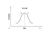
例えばカメラ等のようなレンズを有する撮像装置では、撮影時に図13に示すように映像の高調波成分がピークとなる位置(フォーカスポイント)にレンズを移動させる動作を行う必要があり、この動作(フォーカス)を自動で行うオートフォーカス機能を有する撮像装置が数多く提供されている。 For example, in an imaging apparatus having a lens such as a camera, it is necessary to perform an operation of moving the lens to a position (focus point) where the harmonic component of the image reaches a peak as shown in FIG. Many imaging apparatuses having an autofocus function for automatically performing (focus) are provided.
上記したオートフォーカスを実現する駆動モジュールとして、従来、例えば下記特許文献1に記載されているような、形状記憶合金の温度変化に伴う変形特性を利用してレンズ枠を駆動する駆動モジュールが提案されている。この駆動モジュールには、支持体と、その支持体に対して一定方向に沿って往復移動可能なレンズ枠と、そのレンズ枠を弾性保持するばね部材と、レンズ枠をばね部材の復元力に抗して駆動する駆動手段と、が備えられている。前記した駆動手段には、レンズ枠に係合した回動可能なアーム部と、アーム部に巻き掛けられていると共に両端がそれぞれ固定された形状記憶合金ワイヤと、が備えられている。 As a drive module that realizes the autofocus described above, a drive module that drives a lens frame using a deformation characteristic associated with a temperature change of a shape memory alloy as described in, for example,
上記した従来の駆動モジュールによれば、形状記憶合金ワイヤに通電することで、その通電に伴う発熱によって形状記憶合金ワイヤが縮み変形する。そして、形状記憶合金ワイヤが縮み変形することでアーム部が回動し、そのアーム部によってレンズ枠が押圧され、レンズ枠が一定方向に沿って一方側に移動する。また、上記した通電を停止することで、形状記憶合金ワイヤの温度が低下して形状記憶合金ワイヤが伸び変形する。そして、形状記憶合金ワイヤが伸び変形することでアーム部が戻り方向に回動し、レンズ枠がばね部材の付勢力によってレンズ枠が一定方向に沿って他方側に移動する。 According to the conventional drive module described above, when the shape memory alloy wire is energized, the shape memory alloy wire contracts and deforms due to the heat generated by the energization. When the shape memory alloy wire contracts and deforms, the arm portion rotates, the lens frame is pressed by the arm portion, and the lens frame moves to one side along a certain direction. Further, by stopping the energization described above, the temperature of the shape memory alloy wire is lowered and the shape memory alloy wire is stretched and deformed. When the shape memory alloy wire expands and deforms, the arm portion rotates in the return direction, and the lens frame moves to the other side along a certain direction by the biasing force of the spring member.
また、形状記憶合金の電気抵抗値は、形状記憶合金の変形量と相関があることが知られている。そして、従来より、形状記憶合金の電気抵抗値に基いて形状記憶合金の変形量をモニタリングする技術が知られている(例えば、下記特許文献2参照。)。したがって、上記した形状記憶合金ワイヤの電気抵抗値に基いて形状記憶合金ワイヤの変形量をモニタリングしながら形状記憶合金ワイヤに対する通電を制御することで、形状記憶合金の変形量を調節することができ、レンズ枠をターゲット位置まで移動させることができる。 Further, it is known that the electric resistance value of the shape memory alloy has a correlation with the deformation amount of the shape memory alloy. Conventionally, a technique for monitoring the deformation amount of a shape memory alloy based on the electrical resistance value of the shape memory alloy is known (for example, see Patent Document 2 below). Therefore, the deformation amount of the shape memory alloy can be adjusted by controlling the energization to the shape memory alloy wire while monitoring the deformation amount of the shape memory alloy wire based on the electric resistance value of the shape memory alloy wire described above. The lens frame can be moved to the target position.
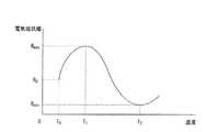
ところで、上記した形状記憶合金の電気抵抗値は、温度変化に対して図14に示すような曲線で変化する。詳しく説明すると、初期温度T0から温度が上昇するのに伴い電気抵抗値が漸次上昇していく。そして、形状記憶合金の変形が開始された時点(温度T1)で電気抵抗値が下降に転じて漸次低下していき、形状記憶合金の変形が限界に達して形状記憶合金の変形が収まった時点(温度T2)で電気抵抗値が再び上昇に転じて漸次上昇する。つまり、形状記憶合金の変形が開始された時点の電気抵抗値Rmaxが最大値となり、形状記憶合金の変形が収まった時点の電気抵抗値Rminが最小値となる。By the way, the electrical resistance value of the shape memory alloy described above changes with a curve as shown in FIG. 14 with respect to the temperature change. More specifically, as the temperature rises from the initial temperature T0 , the electrical resistance value gradually rises. Then, when the deformation of the shape memory alloy is started (temperature T1 ), the electric resistance value starts to decrease and gradually decreases, the deformation of the shape memory alloy reaches the limit, and the deformation of the shape memory alloy is settled. At the time (temperature T2 ), the electric resistance value starts to increase again and gradually increases. That is, the electric resistance value Rmax when the deformation of the shape memory alloy is started becomes the maximum value, and the electric resistance value Rmin when the deformation of the shape memory alloy is stopped becomes the minimum value.
また、上記した従来の駆動モジュールは、例えば、図15に示すように動作させる。すなわち、まず、撮像装置の電源を入れるたびにキャリブレーション動作を行う。すなわち、形状記憶合金ワイヤに通電して当該形状記憶合金ワイヤを限界まで縮み変形させることにより、最大電気抵抗値Rmaxと最小電気抵抗値Rminを検出して駆動モジュールによる動作可能範囲を検出する。次に、最大電気抵抗値Rmaxを指令値にして形状記憶合金ワイヤに対して通電して形状記憶合金ワイヤの電気抵抗を変形開始直前の電気抵抗値まで上昇させる。次に、形状記憶合金ワイヤに対して通電して形状記憶合金ワイヤの電気抵抗を一定幅で段階的に下降させることで、形状記憶合金ワイヤを徐々に縮み変形させてレンズ枠を全移動範囲に亘って移動させる。このとき、画像のコントラストが最も高くなる焦点を探査する。続いて、形状記憶合金ワイヤの電気抵抗を前記した焦点の電気抵抗値まで上昇させて形状記憶合金ワイヤを伸び変形させる。これにより、レンズ枠が合焦位置まで移動し、レンズの焦点が合わせられる。Further, the conventional driving module described above is operated as shown in FIG. 15, for example. That is, first, a calibration operation is performed each time the imaging apparatus is turned on. That is, by energizing the shape memory alloy wire and contracting and deforming the shape memory alloy wire to the limit, the maximum electric resistance value Rmax and the minimum electric resistance value Rmin are detected to detect the operable range by the drive module. . Next, the shape memory alloy wire is energized with the maximum electric resistance value Rmax as a command value, and the electric resistance of the shape memory alloy wire is increased to the electric resistance value immediately before the start of deformation. Next, by energizing the shape memory alloy wire and gradually lowering the electric resistance of the shape memory alloy wire with a certain width, the shape memory alloy wire is gradually contracted and deformed to bring the lens frame into the entire movement range. Move across. At this time, a focus where the contrast of the image is the highest is searched. Subsequently, the shape memory alloy wire is stretched and deformed by increasing the electric resistance of the shape memory alloy wire to the electric resistance value of the focal point. As a result, the lens frame moves to the in-focus position, and the lens is focused.
また、上記した従来の駆動モジュールの動作として、例えば、図16に示すような動作も考えられる。すなわち、まず、上記したキャリブレーション動作を行う。次に、最小電気抵抗値Rminを指令値にして形状記憶合金ワイヤに対して通電して形状記憶合金ワイヤを限界付近まで縮み変形させる。続いて、形状記憶合金ワイヤの電気抵抗を一定幅で段階的に上昇させることで、形状記憶合金ワイヤを徐々に伸び変形させてレンズ枠を全移動範囲に亘って移動させる。このとき、画像のコントラストが最も高くなる焦点を探査する。続いて、形状記憶合金ワイヤの電気抵抗を前記した焦点の電気抵抗値まで低下させて形状記憶合金ワイヤを縮み変形させる。これにより、レンズ枠が合焦位置まで移動し、レンズの焦点が合わせられる。Further, as an operation of the above-described conventional drive module, for example, an operation as shown in FIG. 16 can be considered. That is, first, the above-described calibration operation is performed. Next, the shape memory alloy wire is energized with the minimum electric resistance value Rmin as a command value, and the shape memory alloy wire is contracted and deformed to near the limit. Subsequently, by gradually increasing the electric resistance of the shape memory alloy wire with a certain width, the shape memory alloy wire is gradually extended and deformed to move the lens frame over the entire movement range. At this time, a focus where the contrast of the image is the highest is searched. Subsequently, the shape memory alloy wire is contracted and deformed by reducing the electric resistance of the shape memory alloy wire to the electric resistance value of the focal point. As a result, the lens frame moves to the in-focus position, and the lens is focused.
しかしながら、上記した従来の技術では、形状記憶合金ワイヤの製造時において線径に誤差が生じると、指令値に対する形状記憶合金ワイヤの変形量に個体差が生じる。すなわち、形状記憶合金ワイヤの線径に誤差が生じると、形状記憶合金ワイヤの初期電気抵抗値にばらつきが生じる。通電に対する形状記憶合金ワイヤの感度、つまり単位抵抗あたりに変化する形状記憶合金ワイヤの長さ(ゲイン)は、下記数式1に示すとおり、形状記憶合金ワイヤの初期電気抵抗値に依存するため、上述したように初期電気抵抗値にばらつきが生じると、形状記憶合金ワイヤの感度にもばらつきが生じ、指令値に対する形状記憶合金ワイヤの変形量に個体差が生じる。 However, in the conventional technology described above, if an error occurs in the wire diameter during the manufacture of the shape memory alloy wire, an individual difference occurs in the deformation amount of the shape memory alloy wire with respect to the command value. That is, when an error occurs in the diameter of the shape memory alloy wire, the initial electric resistance value of the shape memory alloy wire varies. The sensitivity of the shape memory alloy wire with respect to energization, that is, the length (gain) of the shape memory alloy wire that changes per unit resistance depends on the initial electrical resistance value of the shape memory alloy wire as shown in

上述したように指令値に対する形状記憶合金ワイヤの変形量に個体差が生じると、形状記憶合金ワイヤの電気抵抗を一定幅で段階的に変化させる際に、レンズ枠の移動幅にばらつきが生じてオートフォーカス精度が確保できないという問題が存在する。例えば、変形量が大きい形状記憶合金ワイヤでは、スキャンの間隔が荒くなりオートフォーカスの精度が確保できないおそれがある。一方、変形量の小さい形状記憶合金ワイヤでは、必要な移動量に要するステップ数が増加し、オートフォーカスが終了するまでの時間が長くなるおそれがある。 As described above, when there is an individual difference in the deformation amount of the shape memory alloy wire with respect to the command value, when the electric resistance of the shape memory alloy wire is changed stepwise by a constant width, the movement width of the lens frame varies. There is a problem that the autofocus accuracy cannot be secured. For example, with a shape memory alloy wire having a large deformation amount, there is a possibility that the scan interval becomes rough and the accuracy of autofocus cannot be ensured. On the other hand, in the shape memory alloy wire with a small deformation amount, the number of steps required for the necessary movement amount increases, and there is a possibility that the time until the autofocus is finished becomes long.
本発明は、上記した従来の問題が考慮されたものであり、形状記憶合金体の形状に誤差があって形状記憶合金体の感度にばらつきがあっても、レンズ枠の移動幅のばらつきを抑制することができ、高いオートフォーカス精度を確保することができる駆動モジュール、電子機器及び駆動モジュールの制御方法を提供することを目的としている。 The present invention takes the above-mentioned conventional problems into consideration, and suppresses variation in the movement width of the lens frame even if the shape memory alloy body has an error and the shape memory alloy body has variations in sensitivity. It is an object of the present invention to provide a drive module, an electronic device, and a drive module control method capable of ensuring high autofocus accuracy.
本発明に係る駆動モジュールは、支持体と、該支持体に対して一定方向に沿って往復移動可能に設けられていると共にレンズを保持するレンズ枠と、該レンズ枠を弾性保持するばね部材と、通電による発熱によって変形可能である形状記憶合金体を有し、該形状記憶合金体が通電により変形することで前記レンズ枠を前記ばね部材の復元力に抗して駆動する駆動手段と、前記レンズ枠が間欠的に移動するように前記形状記憶合金体の電気抵抗の指令値を設定して前記形状記憶合金体に対する通電を制御することで前記駆動手段の駆動制御を行う制御手段と、を備えた駆動モジュールであって、前記制御手段に、前記形状記憶合金体の電気抵抗値を検出する抵抗検出手段と、前記指令値を生成する指令値生成手段と、前記抵抗検出手段によって検出された検出値が前記指令値生成手段によって生成された前記指令値と一致するように前記形状記憶合金に対して通電を行う通電手段と、が備えられており、前記指令値生成手段が、前記レンズ枠を間欠的に移動させる際に前記形状記憶合金体の電気抵抗が一定幅で段階的に上昇又は低下するように一定の変化幅で前記指令値を段階的に変化させると共に、前記形状記憶合金体の電気抵抗の理想基準値に対する前記形状記憶合金体の電気抵抗の実測基準値の比率を補正率とし、該補正率を前記指令値の理想変化幅に乗じて補正変化幅を算出する補正演算を行い、該補正変化幅を前記変化幅として前記指令値を段階的に変化させることを特徴としている。 The drive module according to the present invention is provided with a support, a lens frame that is reciprocally movable along a fixed direction with respect to the support and holds a lens, and a spring member that elastically holds the lens frame. Driving means for driving the lens frame against the restoring force of the spring member by deforming the shape memory alloy body by energization, the shape memory alloy body being deformable by heat generation by energization, Control means for controlling drive of the drive means by setting a command value of the electrical resistance of the shape memory alloy body so that the lens frame moves intermittently and controlling energization to the shape memory alloy body; A drive module comprising: a resistance detection unit that detects an electrical resistance value of the shape memory alloy body; a command value generation unit that generates the command value; and a resistance detection unit. Energization means for energizing the shape memory alloy so that the detected value that is output matches the command value generated by the command value generation means, and the command value generation means, When the lens frame is moved intermittently, the command value is changed stepwise with a constant change width so that the electric resistance of the shape memory alloy body increases or decreases stepwise with a constant width, and the shape The ratio of the measured reference value of the electrical resistance of the shape memory alloy body to the ideal reference value of the electrical resistance of the memory alloy body is used as a correction rate, and the correction change width is calculated by multiplying the correction rate by the ideal change width of the command value. A correction calculation is performed, and the command value is changed stepwise with the correction change width as the change width.
上述した駆動モジュールでは、仮に形状記憶合金体の形状に誤差があって感度にばらつきがあっても、そのばらつきに応じて指令値の変化幅が補正される。例えば、実際の形状記憶合金体のゲインが理想のゲインよりも大きい場合には、その分だけ指令値の変化幅を小さくする補正が行われ、また、実際の形状記憶合金体のゲインが理想のゲインよりも小さい場合には、その分だけ指令値の変化幅を大きくする補正が行われる。これにより、形状記憶合金体の形状に誤差があっても指令値に対する形状記憶合金体の変形量のばらつきが抑えられ、形状記憶合金体の電気抵抗を一定幅で段階的に変化させてレンズ枠を間欠的に移動させる際、レンズ枠が所定の幅で間欠的に移動する。 In the drive module described above, even if there is an error in the shape of the shape memory alloy body and the sensitivity varies, the change width of the command value is corrected according to the variation. For example, when the gain of the actual shape memory alloy body is larger than the ideal gain, correction is performed to reduce the change width of the command value by that amount, and the gain of the actual shape memory alloy body is ideal. If the gain is smaller than the gain, correction is performed to increase the command value change width accordingly. Thereby, even if there is an error in the shape of the shape memory alloy body, variation in the deformation amount of the shape memory alloy body with respect to the command value can be suppressed, and the electric resistance of the shape memory alloy body can be changed step by step with a certain width. When the lens frame is moved intermittently, the lens frame moves intermittently with a predetermined width.
ところで、仮に形状記憶合金体の実測した電気抵抗値が理想基準値よりも小さい場合、その形状記憶合金体のゲインは大きくなるため、形状記憶合金体の電気抵抗を一定幅で段階的に変化させる際にレンズ枠のトータル移動範囲が広くなる。この場合、レンズ枠の1ステップあたりの変形量が大きくなるため合焦精度が多少低下するおそれがあるが、焦点を探査することは可能である。反対に、形状記憶合金体の実測した電気抵抗値が理想基準値よりも大きい場合、その形状記憶合金体のゲインは小さくなるため、形状記憶合金体の電気抵抗を一定幅で段階的に変化させる際にレンズ枠の総移動範囲が狭くなる。この場合、レンズ枠のトータル移動範囲が合焦位置から外れて焦点を探査できなくなるおそれがある。
そこで、本発明に係る駆動モジュールは、前記指令値生成手段が、前記実測基準値が前記理想基準値よりも大きい場合に前記補正変化幅を前記変化幅として前記指令値を段階的に変化させ、前記実測基準値が前記理想基準値以下である場合に前記理想変化幅を前記変化幅として前記指令値を段階的に変化させることが好ましい。
これにより、形状記憶合金体の電気抵抗を一定幅で段階的に変化させる際にレンズ枠のトータル移動範囲が狭くなることがなく、焦点が探査されない不具合が防止される。By the way, if the measured electrical resistance value of the shape memory alloy body is smaller than the ideal reference value, the gain of the shape memory alloy body increases, so that the electrical resistance of the shape memory alloy body is changed stepwise with a certain width. In this case, the total movement range of the lens frame is widened. In this case, although the amount of deformation per step of the lens frame increases, the focusing accuracy may be somewhat lowered, but it is possible to search for the focal point. On the other hand, when the measured electrical resistance value of the shape memory alloy body is larger than the ideal reference value, the gain of the shape memory alloy body is reduced, so that the electrical resistance of the shape memory alloy body is changed stepwise with a constant width. In this case, the total movement range of the lens frame is narrowed. In this case, there is a possibility that the total movement range of the lens frame is out of the in-focus position and the focus cannot be searched.
Therefore, in the drive module according to the present invention, when the command value generation unit has the actual measurement reference value larger than the ideal reference value, the command value is changed stepwise with the correction change width as the change width, When the measured reference value is less than or equal to the ideal reference value, it is preferable that the command value is changed stepwise with the ideal change width as the change width.
Thereby, when the electric resistance of the shape memory alloy body is changed stepwise with a constant width, the total movement range of the lens frame is not narrowed, and the inconvenience that the focus is not searched is prevented.
ところで、形状記憶合金体の変形が開始する温度は、誤作動を防止するために一般的に使用温度範囲よりも高く設定する。よって、電気抵抗値が最大となるとき、形状記憶合金体の温度は少なくとも外気温よりも高くなる。
したがって、本発明に係る駆動モジュールは、前記形状記憶合金体の最大の電気抵抗値を測定して前記実測基準値とすると共に前記形状記憶合金体の理想の最大電気抵抗値を前記理想基準値とすることが好ましい。
これにより、実測基準値の測定の際、形状記憶合金体の温度が外気温よりも高いので、外気温の影響を受けることなく実測基準値が測定される。よって、温度環境に左右されずに正確な補正率を算出することができ、オートフォーカス精度の向上を図ることができる。By the way, the temperature at which deformation of the shape memory alloy body starts is generally set higher than the operating temperature range in order to prevent malfunction. Therefore, when the electrical resistance value is maximized, the temperature of the shape memory alloy body is at least higher than the outside air temperature.
Therefore, the drive module according to the present invention measures the maximum electrical resistance value of the shape memory alloy body to be the actual measurement reference value and sets the ideal maximum electrical resistance value of the shape memory alloy body as the ideal reference value. It is preferable to do.
Thereby, when measuring the actual measurement reference value, since the temperature of the shape memory alloy body is higher than the outside air temperature, the actual measurement reference value is measured without being influenced by the outside air temperature. Therefore, an accurate correction factor can be calculated regardless of the temperature environment, and the autofocus accuracy can be improved.
また、本発明に係る駆動モジュールは、焦点検出動作前のキャリブレーション動作中に前記抵抗検出手段で前記形状記憶合金体の電気抵抗値を測定することで前記実測基準値を取得することが好ましい。
これにより、製造時に形状記憶合金体の電気抵抗値を予め測定する必要がなく、量産性を向上させることができる。The drive module according to the present invention preferably obtains the actual measurement reference value by measuring the electrical resistance value of the shape memory alloy body with the resistance detection means during the calibration operation before the focus detection operation.
Thereby, it is not necessary to measure the electrical resistance value of the shape memory alloy body in advance at the time of manufacture, and mass productivity can be improved.
また、本発明に係る駆動モジュールは、前記指令値生成手段が、製造時に予め測定された前記実測基準値に基づいて前記補正率を算出するものであってもよい。
このように製造時に実測基準値を測定することにより、一定の温度環境下で実測基準値を測定することが可能であるので、温度環境の違いによる実測基準値のばらつきが抑制される。よって、温度環境に左右されずに正確な補正率を算出することができ、オートフォーカス精度の向上を図ることができる。In the drive module according to the present invention, the command value generation unit may calculate the correction factor based on the actual measurement reference value measured in advance at the time of manufacture.
By measuring the actual measurement reference value at the time of manufacturing in this way, it is possible to measure the actual measurement reference value under a constant temperature environment, so that variations in the actual measurement reference value due to differences in temperature environment are suppressed. Therefore, an accurate correction factor can be calculated regardless of the temperature environment, and the autofocus accuracy can be improved.
また、本発明に係る電子機器は、上記した駆動モジュールを備えたことを特徴としている。
この電子機器では、形状記憶合金体の形状に誤差があって感度にばらつきがあっても、そのばらつきに応じて指令値の変化幅が補正されるので、電子機器のオートフォーカス精度が高くなる。In addition, an electronic apparatus according to the present invention includes the drive module described above.
In this electronic device, even if there is an error in the shape of the shape memory alloy body and the sensitivity varies, the change width of the command value is corrected according to the variation, so that the autofocus accuracy of the electronic device is increased.
また、本発明に係る駆動モジュールの制御方法は、支持体と、該支持体に対して一定方向に沿って往復移動可能に設けられていると共にレンズを保持するレンズ枠と、該レンズ枠を弾性保持するばね部材と、通電による発熱によって変形可能である形状記憶合金体を有し、該形状記憶合金体が通電により変形することで前記レンズ枠を前記ばね部材の復元力に抗して駆動する駆動手段と、前記レンズ枠が間欠的に移動するように前記形状記憶合金体の電気抵抗の指令値を設定して前記形状記憶合金体に対する通電を制御することで前記駆動手段の駆動制御を行う制御手段と、を備えた駆動モジュールの制御方法であって、前記レンズ枠を間欠的に移動させる際に、前記形状記憶合金体の電気抵抗が一定幅で段階的に上昇又は低下するように一定の変化幅で前記指令値を段階的に変化させると共に、前記形状記憶合金体の電気抵抗の理想基準値に対する前記形状記憶合金体の電気抵抗の実測基準値の比率を補正率とし、該補正率を前記指令値の理想変化幅に乗じて補正変化幅を算出する補正演算を行い、該補正変化幅を前記変化幅として前記指令値を段階的に変化させることを特徴としている。 The drive module control method according to the present invention includes a support, a lens frame that is reciprocally movable along a fixed direction with respect to the support, and a lens frame that holds the lens, and the lens frame is elastic. A holding spring member and a shape memory alloy body that can be deformed by heat generated by energization, and the shape memory alloy body is deformed by energization to drive the lens frame against the restoring force of the spring member. Driving control of the driving means is performed by setting a command value of the electrical resistance of the shape memory alloy body so that the driving means and the lens frame move intermittently and controlling energization to the shape memory alloy body And a control means for controlling the drive module, wherein when the lens frame is moved intermittently, the electrical resistance of the shape memory alloy body is increased or decreased stepwise with a constant width. The command value is changed in a stepwise manner with a change width, and a ratio of the measured reference value of the electrical resistance of the shape memory alloy body to the ideal reference value of the electrical resistance of the shape memory alloy body is set as a correction rate, and the correction rate The correction value is calculated by multiplying the command value by the ideal change width, and the command value is changed stepwise by using the correction change width as the change width.
このような駆動モジュールの制御方法では、仮に形状記憶合金体の形状に誤差があって感度にばらつきがあっても、そのばらつきに応じて指令値の変化幅が補正されるので、指令値に対する形状記憶合金体の変形量が一定となり、形状記憶合金体の電気抵抗を一定幅で段階的に変化させる際の形状記憶合金体の変形量が一定となる。 In such a control method of the drive module, even if there is an error in the shape of the shape memory alloy body and the sensitivity varies, the change width of the command value is corrected according to the variation. The deformation amount of the memory alloy body becomes constant, and the deformation amount of the shape memory alloy body when the electric resistance of the shape memory alloy body is changed stepwise with a constant width becomes constant.
本発明に係る駆動モジュール、電子機器及び駆動モジュールの制御方法によれば、形状記憶合金体の形状に誤差があって形状記憶合金体の感度にばらつきがあっても、レンズ枠の移動幅のばらつきを抑制することができ、高いオートフォーカス精度を確保することができる。 According to the drive module, the electronic apparatus, and the drive module control method according to the present invention, even if there is an error in the shape memory alloy shape and the sensitivity of the shape memory alloy body varies, the variation in the movement width of the lens frame. Can be suppressed, and high autofocus accuracy can be secured.
以下、本発明に係る駆動モジュール、電子機器及び駆動モジュールの制御方法の実施の形態について、図面に基いて説明する。
なお、一部の図面では見易さのため、例えば図5に示すレンズユニット12などの構成部材を適宜省略して図示している。
また、図中の符号Mは、図5に示すレンズ50の光軸に一致する駆動モジュール1の仮想的な軸線であり、後述するレンズ枠4の駆動方向を示している。以下では、説明を簡単にするため、分解された各構成部材の説明においても、組立時の軸線Mとの位置関係に基づいて、位置や方向を参照する場合がある。例えば、構成部材に明確な円、円筒面が存在しない場合でも、誤解のおそれのない限り、軸線Mに沿う方向を単に「軸方向」と称し、軸線Mに直交する方向を単に「径方向」と称し、軸線M回りの方向を単に「周方向」と称する場合がある。また、軸方向のうちの後述する制御基板32側を「下方」とし、その反対側を「上方」とする。Embodiments of a drive module, an electronic apparatus, and a drive module control method according to the present invention will be described below with reference to the drawings.
For ease of viewing in some drawings, for example, components such as the
A symbol M in the figure is a virtual axis line of the
まず、本実施形態における駆動モジュール1の構成について説明する。
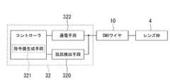
図1、2に示すように、本実施形態の駆動モジュール1は、図5に示すレンズ12(レンズユニット12)を軸方向に沿って往復移動させるための駆動モジュールであり、電子機器などに搭載されるものである。この駆動モジュール1は、制御手段となる制御基板32と、制御基板32上に位置するアダプタ30と、アダプタ30上に配設される駆動ユニット31と、駆動ユニット31を覆うように配設されたカバー11と、を備えている。First, the structure of the
As shown in FIGS. 1 and 2, the
図3に示すように、駆動ユニット31は、被駆動体となるレンズ枠4、支持体となるモジュール枠5、ばね部材となる上板ばね6と下板ばね7、モジュール下板8、給電部材9、及び形状記憶合金体となる形状記憶合金(Shape Memory Alloy、以下、SMAと略称する)ワイヤ10を主な構成部材とするものであって、これら構成部材が一体に組み立てられることで1つのアクチュエータを構成する。 As shown in FIG. 3, the
図3〜5に示すように、上記したレンズ枠4はモジュール枠5の内側に軸方向に移動可能に挿入されており、これらレンズ枠4とモジュール枠5の上端部に上板ばね6が配設されていると共にレンズ枠4とモジュール枠5の下端部に下板ばね7が配設されており、これらの上板ばね6及び下板ばね7によってレンズ枠4及びモジュール枠5が挟持されている。上板ばね6はレンズ枠4及びモジュール枠5の各上端部にそれぞれ加締めにより固定されている。また、下板ばね7の下方にはモジュール下板8が積層されており、そのモジュール下板8の下方には給電部材9が積層されており、これら下板ばね7、モジュール下板8及び給電部材9はモジュール枠5の下端部に加締めによりそれぞれ共に固定され、さらに、下板ばね7はレンズ枠4の下端部に加締めにより固定されている。また、上記したモジュール下板8の上面に上記したカバー11が載置されて固定されている。 As shown in FIGS. 3 to 5, the
上記したレンズ枠4は、軸線Mを中心軸線として軸方向に沿って延設された略円筒形状の筒状部材であり、図5に示すように、軸方向に貫通する横断面視円形の収容部4Aの内周面4Fに雌ネジが形成されている。そして、収容部4Aの内周面4Fにはレンズユニット12が螺合されており、これによりレンズユニット12がレンズ枠4に保持されている。なお、レンズユニット12は、外周面に雄ネジが形成された円筒形状の筒部51と、その筒部51の内側に嵌合されたレンズ50と、から構成されている。 The
レンズ枠4の外壁面4Bには周方向に略90度の間隔をおいて、径方向外方に向けて突出する突出部4C(凸部)が軸方向に延設されており、それら各突出部4Cの上端面4aと下端面4bには、上側固定ピン13A、下側固定ピン13Bがそれぞれ立設されている。上側固定ピン13Aは上板ばね6を保持し、下側固定ピン13Bは下板ばね7を保持するためのものである。 On the
上側固定ピン13A及び下側固定ピン13Bは、軸線Mに平行な同軸位置に配置されているため、上板ばね6及び下板ばね7における、上側固定ピン13A及び下側固定ピン13Bの挿通位置はそれぞれ共通化されている。
なお、上側固定ピン13Aおよび下側固定ピン13Bの平面視の位置が異なっていてもよく、例えば4本の突出部4Cのうちの2つの突出部4Cの各上端面4aに上側固定ピン13Aをそれぞれ立設し、残りの2本の突出部4Cの各上端面4aに下側固定ピン13Bをそれぞれ立設してもよい。Since the
Note that the positions of the
レンズ枠4には、SMAワイヤ10を掛けられるガイド突起4Dが設けられている。このガイド突起4Dは、複数の突出部4Cのうちの1つの下端部の外周面に一体に接合されており、SMAワイヤ10が掛けられて係止する先端鍵部(係止部)4D1が形成されている。この先端鍵部4D1は、そこに掛けられたSMAワイヤ10が収縮することによりレンズ枠4を上方に持ち上げて軸方向に沿って上方に移動させるものである。 The
また、レンズ枠4には、レンズ枠4を下向きに付勢する図2に示すコイルスプリング34を保持するスプリング保持部33が設けられている。このスプリング保持部33はガイド突起4Dの上端面に立設された柱状の凸部であり、このスプリング保持部33には図2に示すコイルスプリング34が挿通されている。これによりSMAワイヤ10が周囲環境の影響などにより収縮してレンズ枠4を上昇させようとする動きを抑制することができる。なお、レンズ枠4は、熱加締めまたは超音波加締めが可能な熱可塑性樹脂、例えばポリカーボネート(PC)、液晶ポリマー(LCP)樹脂などにより一体成形されている。 Further, the
モジュール枠5は、軸線Mを中心軸線として軸方向に沿って延設された筒状部材であり、平面視の外形が全体として略矩形状に形成され、かつその中央部に、軸方向に貫通する横断面視円形の収容部5Aが形成されている。この収容部5A内には、上記したレンズ枠4が収容されている。モジュール枠5の上部及び下部の四隅には、軸線Mに対する仮想垂直に沿って形成された平面状の上下端面5a、5bがそれぞれ形成され、各上端面5aには上側固定ピン14Aが上方に向けてそれぞれ突設され、各下端面5bには下側固定ピン14Bが下方に向けてそれぞれ突設されている。 The
上側固定ピン14Aは上板ばね6を保持し、下側固定ピン14Bは下板ばね7、モジュール下板8及び給電部材9を保持するためのものである。なお、上側固定ピン14Aの平面視の位置は、下側固定ピン14Bの配置と異なっていてもよいが、本実施形態では、それぞれ軸線Mに平行な同軸位置に配置されている。このため、上板ばね6、下板ばね7における、上側固定ピン14A及び下側固定ピン14Bの挿通位置は、それぞれ共通化されている。また、上記した上下端面5a、5bの間の距離は、レンズ枠4の上下端面4a、4bの間の距離と略同一距離に設定されている。 The
モジュール枠5の一隅の下部には平面視の溝幅がレンズ枠4のガイド突起4Dに軸方向に移動可能に嵌合する大きさを有する切欠き5Bが形成されている。この切欠き5Bは、レンズ枠4をモジュール枠5内に下方から挿入して収容した状態で、レンズ枠4のガイド突起4Dを貫通させ、ガイド突起4Dの先端鍵部4D1をモジュール枠5の径方向外部に突出させるとともに、レンズ枠4の周方向の位置決めを行うためのものである。 A
また、図3、4に示すように、モジュール枠5の切欠き5Bに隣り合う2つの隅部には、切欠き5Bが設けられた隅部と同方向側の側面において、SMAワイヤ10を保持するワイヤ保持部材(保持端子)15A、15Bを取り付けるための一対の係止溝5Cが形成されている。 As shown in FIGS. 3 and 4, the
モジュール枠5の側面におけるワイヤ保持部材15A,15Bが配される位置には、ピン35A,35Bがそれぞれ形成されている。さらに、ピン35A,35Bが形成された下方には、接着剤が充填されてモジュール枠5とワイヤ保持部材15A,15Bとを固定する溝部36が形成されている。そして、ワイヤ保持部材15A,15Bをモジュール枠5に固定する際に、ワイヤ保持部材15A,15Bが回動するのを抑制することができる壁部35Cが形成されている。壁部35Cは、モジュール枠5の側面から側方(側面に対して鉛直方向)に延出されている。
また、モジュール枠5は、本実施形態ではレンズ枠4と同様に、熱加締めまたは超音波加締めが可能な熱可塑性樹脂、例えばポリカーボネート(PC)、液晶ポリマー(LCP)樹脂などにより一体成形されている。 Further, in the present embodiment, the
ワイヤ保持部材15Aは、駆動モジュール1から給電部材9の一対の端子部9Cが突出される側の側面に取り付けられ、ワイヤ保持部材15Bは、駆動モジュール1から給電部材9の一対の端子部9Cが突出されない側の側面に取り付けられている。 The
図4に示すように、ワイヤ保持部材15A、15Bは、ワイヤ保持部15bにSMAワイヤ10の端部を加締めてなる鍵状に形成された金属板などの導電性部材である。ワイヤ保持部材15A,15Bには、モジュール枠5のピン35A,35Bに嵌合する貫通孔36A,36Bがそれぞれ形成されている。また、貫通孔36A,36Bの軸方向下方には接着剤を流し込むための貫通孔37A,37Bがそれぞれ形成されている。そして、モジュール枠5とワイヤ保持部材15A,15Bとを固定する際に、モジュール枠5の壁部35Cに当接して、ワイヤ保持部材15A,15Bの回動を抑止するための腕部38A,38Bがそれぞれ形成されている。係止溝5Cおよびピン35A,35Bに側方から嵌合させ、壁部35Cと腕部38A,38Bとを当接させることで、SMAワイヤ10の端部を位置決めして保持するものである。 As shown in FIG. 4, the wire holding members 15 </ b> A and 15 </ b> B are conductive members such as a metal plate formed in a key shape formed by caulking the end portion of the
ワイヤ保持部材15A、15Bは、SMAワイヤ10のワイヤ保持部15b(加締め位置)と反対側に片状の端子部15aを備え、モジュール枠5に対する取付状態において、端子部15aがモジュール枠5の下方に積層されたモジュール下板8の下方にわずかに突出されるようになっている。 The wire holding members 15 </ b> A and 15 </ b> B are provided with a piece-
また、一対のワイヤ保持部材15A、15Bによって両端が保持されたSMAワイヤ10は、モジュール枠の切欠き5Bから突出されたレンズ枠4のガイド突起4Dの先端鍵部4D1に下方から係止され、SMAワイヤ10の張力により、先端鍵部4D1を介して、レンズ枠4を上方に付勢している。 Further, the
図3,4に示すように、モジュール枠5及びモジュール枠5内に挿入されたレンズ枠4のそれぞれの上部と下部には、それぞれ上板ばね6と下板ばね7とが積層されている。上板ばね6及び下板ばね7は、略同一形状に打ち抜かれた平板状の板ばね部材であり、例えば、ステンレス(SUS)鋼板などの金属板からなる。 As shown in FIGS. 3 and 4, an
上板ばね6(下板ばね7)の形状は、平面視の外形が、モジュール枠5の上側(下側)の端部と同様な略矩形状とされ、中央部に軸線Mと同軸でレンズ枠4の内周面4Fよりわずかに大きな円状の開口6C(7C)が形成され、全体としてリング状とされている。 The shape of the upper leaf spring 6 (lower leaf spring 7) has a substantially rectangular shape in plan view, similar to the upper (lower) end of the
上板ばね6(下板ばね7)の隅部近傍には、モジュール枠5の隅部近傍に形成された上側固定ピン14A(下側固定ピン14B)の配置位置に対応して、各上側固定ピン14A(下側固定ピン14B)にそれぞれ挿通可能な4つの貫通孔6B(7B)が形成されている。これにより、モジュール枠5に対する軸線Mに直交する平面内の位置決めが可能となっている。 In the vicinity of the corner of the upper leaf spring 6 (lower leaf spring 7), the upper fixing pins 14A (lower fixing
また、上板ばね6(下板ばね7)には、レンズ枠4に形成された上側固定ピン13A(下側固定ピン13B)の配置位置に対応して、各上側固定ピン13A(下側固定ピン13B)にそれぞれ挿通可能な4つの貫通孔6A(7A)が形成されている。 Further, the upper plate spring 6 (lower plate spring 7) has upper fixing pins 13A (lower fixing pins) corresponding to the positions of the upper fixing pins 13A (lower fixing
また、開口6C(7C)の径方向外側には、リング部6F(7F)が形成され、軸線Mを挟んで互いに対角方向に対向する貫通孔6A(7A)の近傍位置から、周方向に略半円弧状に延びる4つのスリット6D(7D)がそれぞれ、略四分円弧ずつ径方向に重なった状態に形成されている。 Further, a
これにより、上板ばね6(下板ばね7)の外側の矩形状枠体から、略四分円弧状に延ばされた4つのばね部6E(7E)が、それぞれ1つずつ貫通孔6A(7A)近傍に延ばされた板ばね部材が形成されている。 Thereby, four
このように、上板ばね6(下板ばね7)の外形が、モジュール枠5の外形に略合わせた矩形状に設けられ、ばね部6E(7E)、リング部6F(7F)が開口6C(7C)に沿うリング状の領域に形成されている。そして、上板ばね6(下板ばね7)をモジュール枠5に固定する上側固定ピン14A(下側固定ピン14B)の配置に応じて、スペースに余裕のある隅部に被固定部である貫通孔6B(7B)が設けられるため、貫通孔6B(7B)の形状が、ばね部6E(7E)から離すことができるので、精密な打ち抜きによる製造やエッチングでの製造が容易となる。 Thus, the outer shape of the upper leaf spring 6 (lower leaf spring 7) is provided in a rectangular shape substantially matching the outer shape of the
モジュール下板8は、モジュール枠5の各下側固定ピン14Bを下板ばね7の貫通孔7Bに貫通させるとともに、モジュール枠5内に収容したレンズ枠4の各下側固定ピン13Bを下板ばね7の貫通孔7Aに貫通させた状態で、モジュール枠5との間で、下板ばね7を下方側から挟んで積層し、下板ばね7の矩形状の外形枠をモジュール枠5の端面5bに対して押圧状態に固定するものである。 The module
モジュール下板8の形状は、モジュール枠5の外形と略同様の矩形状外形を有する板状部材であり、中央部に軸線Mを中心とする略円形状の開口8Aが厚さ方向に貫通して形成されている。そして、組立時に下板ばね7に積層される上面8a側には、レンズ枠4の各下側固定ピン13Bの配置位置に対応する位置に、後述する加締め部との干渉を避けるための4つのU字状の凹部8Bが形成されている。また、モジュール下板8の周縁に位置する各隅部にはモジュール枠5の各下側固定ピン14Bの配置位置に対応して、これら下側固定ピン14Bをそれぞれ挿通させる貫通孔8Cが形成されている。モジュール下板8の材質は、例えば、電気絶縁性および遮光性を有する合成樹脂を採用している。また、モジュール下板8が電気絶縁性を有することで、給電部材9を下板ばね7に対して電気的絶縁状態で固定する絶縁部材となっている。 The shape of the module
給電部材9は、それぞれ板状の金属板からなる一対の電極9a、9bからなる。電極9a、9bは、いずれも、モジュール下板8の外形に沿う略L字状の配線部9Bと、配線部の端部からモジュール下板8の外形の外側に突出する端子部9Cとを備える折れ線状の金属板からなる。そして、それぞれの配線部9Bには、モジュール下板8の下面から下方に突出されるモジュール枠5の下側固定ピン14Bのうち、モジュール下板8の外形に沿って隣り合う2つの下側固定ピン14Bを、それぞれ挿通させて、電極9a、9bをモジュール枠5に対して位置決めを行う2つの貫通孔9Aが設けられている。 The
また、図4に示すように、一対の電極9a、9bの端子部9Cは、モジュール枠5において、ワイヤ保持部材15Aが取り付けられた側の側面から軸方向下方に並列して突出するように設けられている。
このため、一方の電極9aには、貫通孔9Aと端子部9Cとの間の配線部9B上の側面に、ワイヤ保持部材15Aの端子部15aを電気的に接続するために凹状に切り欠かれた導電接続部9Dが設けられている。
これに対し、他方の電極9bには、配線部9Bの側面におけるワイヤ保持部材15Bの端子部15aとの接続箇所に、切り欠かれた導電接続部9Dが形成されている。この導電接続部9Dにおいて、他方の電極9bとワイヤ保持部材15Bとが電気的に接続されている。
また、それぞれの導電接続部9Dを、端子部15aと電気的に接続する手段としては、例えば、半田付けまたは導電性接着剤による接着を採用することができる。Further, as shown in FIG. 4, the
Therefore, one
On the other hand, the
Moreover, as means for electrically connecting each
図2にように、カバー11は、上面11Eの外縁部から下方側に、モジュール枠5を外嵌可能に覆う側壁部11Dが延ばされ、下方側に矩形状の開口11Cが形成された部材であり、上面11Eの中央部に軸線Mを中心とした円状の開口11Aが設けられている。開口11Aの大きさは、レンズユニット12を出し入れ可能な大きさとされる。 As shown in FIG. 2, the
図1,2に示すように、制御基板32は、SMAワイヤ10の電気抵抗の指令値を設定してSMAワイヤ10に対する通電を制御することで駆動ユニット31の駆動制御を行う制御手段であり、駆動ユニット31に制御信号や電力を供給する基板である。この制御基板32の概略構成としては、一対の電極9a、9bの各端子部9Cに電気的に接続されるプリント配線39,39が表面に形成されたプリント基板と、そのプリント基板上に実装された図示しない制御回路と、からなる。詳しく説明すると、制御基板32は、プリント配線39,39を介して一対の電極9a、9bに通電してSMAワイヤ10を適宜伸縮変形させる制御手段であり、SMAワイヤ10を伸縮させることでレンズ枠4をモジュール枠5に対して相対的に軸方向に沿って移動させてレンズ枠4を所望の位置(合焦位置)に配置させるものである。 As shown in FIGS. 1 and 2, the
上記した制御基板32には、図6に示すように、SMAワイヤ10の電気抵抗値を検出する抵抗検出手段320と、SMAワイヤ10の制御の指令値Rtを生成する指令値生成手段321と、抵抗検出手段320によって検出された検出値Rが指令値生成手段321によって生成された指令値Rtと一致するようにSMAワイヤ10に対して通電を行う通電手段322と、が備えられている。As shown in FIG. 6, the
次に、上記した構成の駆動モジュール1の組立方法について順を追って説明する。 Next, the assembly method of the
第1工程では、まず、モジュール枠5の収容部5A内に下方からレンズ枠4を挿入し、モジュール枠5の上端面5aと、レンズ枠4の上端面4aとを同一高さに揃える。そして、モジュール枠5の各上側固定ピン14Aとレンズ枠4の各上側固定ピン13Aとを上板ばね6の各貫通孔6B、6Aにそれぞれ挿通する。 In the first step, first, the
その後、上板バネ6の各貫通孔6A、6Bを貫通して上方に突き出された各上側固定ピン13A、14Aの先端部を図示しないヒータチップにより熱加締めして、図4、5に示すようにそれぞれ第1の固定部である加締め部16と、第2の固定部である加締め部17を形成する。 Thereafter, the tips of the upper fixing pins 13A and 14A protruding through the through
このとき、レンズ枠4の上端面4aとモジュール枠5の上端面5aとは、同一平面上に整列されており、平板状の上板ばね6を変形させることなく配置して、熱加締めを行うことができる。そのため、変形する上板ばね6を押さえる必要がないので、容易に加締め作業を行うことができる。また、上板ばね6の変形による浮きなどの発生を防止することができる。
また、各ヒータチップの高さを共通とすることができるので、双方の加締め部16、17を同時に形成しても、加締め精度のバラツキを低減することができる。At this time, the
Moreover, since the height of each heater chip can be made common, even if both the crimping
次に、第2工程では、レンズ枠4の各下側固定ピン13Bを下板ばね7の各貫通孔7Aにそれぞれ挿通する。その際、同時にモジュール枠5の各下側固定ピン14Bを下板ばね7の各貫通孔7B、モジュール下板8の各貫通孔8C、給電部材9の各貫通孔9Aに挿通する。その後、下板ばね7の各貫通孔7Aを貫通して下方に突き出された各下側固定ピン13Bの先端部を図示しないヒータチップにより熱加締めして、図5に示すように第1の固定部である加締め部18を形成する。 Next, in the second step, the lower fixing pins 13B of the
このとき、レンズ枠4の上下端面4a、4b間の軸方向距離と、モジュール枠5の上下端面5a、5b間の軸方向距離とは等しいため、各下端面4b、5b同士は、同一平面上に整列されており、平板状の下板ばね7を変形させることなくモジュール下板8を積層配置して熱加締めを行うことができるので、下板ばね7の変形による浮きなどの発生を防止することができる。
また、各ヒータチップの高さを共通とすることができるので、加締め部18を同時に形成しても、加締め精度のバラツキを低減することができる。At this time, since the axial distance between the upper and
Moreover, since the height of each heater chip can be made common, even if the
次に、第3工程では、これら貫通孔7B、8C、9Aを貫通して下方に突き出された各下側固定ピン14Bの下端部を図示しないヒータチップにより熱加締めして、図5に示すように第2の固定部である加締め部19を形成する。 Next, in the third step, the lower end portion of each
このとき、各ヒータチップの高さを共通とすることができるため、加締め部19を同時に形成しても、加締め精度のバラツキを低減することができる。
また、モジュール下板8に凹部8Bが形成されているため、第2工程で形成された加締め部18は、モジュール下板8とは接触しない。At this time, since the height of each heater chip can be made common, even if the
Further, since the
これら第1〜第3工程の作業を行うことによって、レンズ枠4とモジュール枠5の両端部に、上板ばね6、下板ばね7、モジュール下板8、給電部材9が積層固定される。 By performing the operations in the first to third steps, the
なお、上側固定ピン13Aと下側固定ピン13B、また上側固定ピン14Aと下側固定ピン14Bが、それぞれ同軸に設けられているため、第1〜第3工程の加締めにおいて、加締め部16、18、加締め部17、19をそれぞれ形成するためのヒータチップの平面上の位置がそれぞれ共通となる。そのため、各加締めにおいて、ヒータチップ位置を変更する必要がないため効率よく加締め作業を行うことができる。 Since the
次に、第4工程(配設工程)では、SMAワイヤ10が取り付けられた一対のワイヤ保持部材15A、15Bを、モジュール枠5に固定する。具体的には、モジュール枠5に形成された2箇所のピン35A,35Bにワイヤ保持部材15A,15Bの貫通孔36A,36Bを嵌合するとともに、係止溝5Cにワイヤ保持部材15A,15Bをそれぞれ係止させる。その際、SMAワイヤ10の中央部を、ガイド突起4Dの先端鍵部4D1に係止させ、かつ、この先端鍵部4D1を下側から支持するように掛け渡す。また、ワイヤ保持部材15A、15Bの各端子部15aは、モジュール下板8の下方に突出され、それぞれ、モジュール下板8に固定された給電部材9である電極9a、9bの導電接続部9Dに係止されるか、もしくは近接して配置されている。 Next, in a fourth step (arrangement step), the pair of wire holding members 15 </ b> A and 15 </ b> B to which the
次に、第5工程(固定工程)では、貫通孔37A,37Bに熱硬化性接着剤を流し込み、モジュール枠5の溝部36内に充填する。溝部36に熱硬化性接着剤を充填したら、その接着剤を硬化させるために加熱炉の中に入れる。加熱炉内において、例えば約100℃で20〜30分程度加熱することにより接着剤が硬化してモジュール枠5とワイヤ保持部材15A,15Bとが接着固定される。 Next, in the fifth step (fixing step), a thermosetting adhesive is poured into the through holes 37 </ b> A and 37 </ b> B and filled in the
n
モジュール枠5とワイヤ保持部材15A,15Bとを接着固定した後、例えば、半田付けや導電性接着剤などを用いて、各端子部15aを、それぞれ導電接続部9Dに対して電気的に接続させる。n
After the
次に、第6工程では、モジュール枠5の上方から、カバー11を被せ、側壁部11Dとモジュール下板8とを接合する。例えば、側壁部11Dに係合爪などを設けてはめ込みによって接合したり、側壁部11Dとモジュール下板8とを接着、または溶着して接合したりする。また、加締め部16、17は、それぞれカバー11の上面11Eの裏面に対して、離間された状態にある。
以上で、駆動モジュール1本体の組み立てが完了する。Next, in the sixth step, the
This completes the assembly of the
その後、駆動ユニット31の下方にアダプタ30を取り付けた後、基板上へ取り付ける。駆動モジュール1の基板上への取り付けは、接着、嵌め込みなどの固定手段を採用することができる。なお、基板は、駆動モジュール1に付属する独立した部材であってもよいし、電子機器等に接続、配置された部材であってもよい。 Thereafter, the
さらに、カバー11の開口11Aを通じてレンズ枠4内にレンズユニット12を螺合して取り付ける。このように、レンズユニット12を最後に取り付けているのは、組立作業により、レンズユニット12のレンズが汚れたり、ゴミなどが付着したりしないためであるが、例えば、駆動モジュール1をレンズユニット12が取り付けられた製品状態で出荷する場合や、カバー11の開口11Aをレンズユニット12の外形より小さくしたい場合、例えば開口絞りを兼用するような場合などには、この工程を、早い段階(第6工程の前)で実施してもよい。 Further, the
次に、上記した駆動モジュール1の動作について説明する。 Next, the operation of the
駆動モジュール1は、端子部9Cに電力が供給されない状態では、SMAワイヤ10からの張力およびコイルスプリング34の付勢力、加締め部16、18で上板ばね6及び下板ばね7からの復元力などのレンズ枠4に作用する力がつり合い、レンズユニット12が取り付けられたレンズ枠4が、軸方向の一定位置に保持される。 In the state where electric power is not supplied to the
上記した駆動モジュール1を駆動させる際には、後述する制御方法に従って制御基板32から端子部9Cを介して給電部材9に電力を供給する。このとき、電極9a、ワイヤ保持部材15A、SMAワイヤ10、ワイヤ保持部材15B及び電極9bは、それぞれ導通されているため、SMAワイヤ10に電流が流れる。 When driving the
したがって、SMAワイヤ10に対して通電すると、SMAワイヤ10にジュール熱が発生して、SMAワイヤ10の温度が上昇し、SMAワイヤ10の変態開始温度を超えると、SMAワイヤ10が温度に応じた長さに収縮する。この結果、レンズ枠4のガイド突起4Dが、上方に移動する。これにより、コイルスプリング34、上板ばね6及び下板ばね7が、それぞれ変形し、変形量に応じた弾性復元力がレンズ枠4に付勢される。そして、この弾性復元力がSMAワイヤ10の張力とつり合う位置でレンズ枠4が停止する。このとき、上板ばね6、下板ばね7は、平行ばねを構成しているため、レンズ枠4は、軸方向のガイド部材などに沿わせなくても、正確に軸線M上に沿って移動される。このため、部品点数を削減し、小型化することが可能となっている。また、ガイド部材に対する摺動負荷も発生しないので、低消費電力を実現することが可能となる。 Therefore, when the
一方、電力の供給を停止してSMAワイヤ10に対する通電を停止すると、SMAワイヤ10が伸長可能となり、レンズ枠4は、下方のつり合い位置まで移動する。
このようにして、制御基板32によって電力供給量を制御することで、レンズ枠4を軸線M方向に駆動する。
なお、SMAワイヤ10は昇温時と降温時との間で温度ヒステリシスが現れるが、ソフト等で補正することで対応可能である。On the other hand, when the supply of power is stopped and the energization to the
In this manner, the
In the
次に、駆動モジュール1の制御方法について説明する。 Next, a method for controlling the
上記した構成からなる駆動モジュール1は制御基板32によって図7、8に示す方法でオートフォーカス動作することが可能である。 The
まず初めに、図7に示すように、SMAワイヤ10の電気抵抗値(実測基準値R0)を実測する。詳しく説明すると、図8に示すように、電子機器の電源を入れるたびにキャリブレーション動作を行う。すなわち、SMAワイヤ10に通電して当該SMAワイヤ10を一旦限界まで縮み変形させてレンズ枠4を最大まで移動させた後、SMAワイヤ10に対する通電を停止してSMAワイヤ10の温度を低下させ、SMAワイヤ10を伸び変形させてレンズ枠4を元の基準位置(下側の基準位置)に戻す。このとき、実測基準値R0として抵抗検出手段320によってSMAワイヤ10の最大電気抵抗値Rmaxを検出する。また、抵抗検出手段320によってSMAワイヤ10の最小電気抵抗値Rminを検出してその最小電気抵抗値Rminと前記した最大電気抵抗値Rmaxとに基づいて駆動モジュール1による動作可能範囲(SMAワイヤ10の伸縮範囲)を検出する。First, as shown in FIG. 7, the electrical resistance value (measurement reference value R0 ) of the
次に、SMAワイヤ10の電気抵抗を一定幅で段階的に低下させることでレンズ枠4を全移動範囲に亘って移動させて焦点を探査する。このとき、上記した指令値生成手段321によって指令値Rtを生成し、抵抗検出手段320によってSMAワイヤ10の検出値Rをフィードバックしながら上記指令値Rtに基づいて通電手段322によってSMAワイヤ10に対して通電を行う。Next, the focal point is searched by moving the
詳しく説明すると、まず、指令値生成手段321において、レンズ枠4を一定幅で間欠的に移動させるためのSMAワイヤ10の電気抵抗値の変化幅ΔRを、上記実測基準値R0及びSMAワイヤ10の電気抵抗の理想基準値Rstan並びに指令値Rtの理想変化幅Rstepに基いて算出する。具体的に説明すると、理想基準値Rstan に対する実測基準値R0の比率を補正率(R0/Rstan)とし、その補正率を理想変化幅Rstepに乗じて補正変化幅(R0/Rstan×Rstep)を算出する補正演算を行う。More specifically, first, in the command value generation means 321, the change width ΔR of the electrical resistance value of the
上記した実測基準値R0は、上述したとおり抵抗検出手段320によって検出されたSMAワイヤ10の最大電気抵抗値Rmaxである。
また、上記した理想基準値Rstanは、SMAワイヤ10の理想の最大電気抵抗値であり、線径ばらつき中央の最大電気抵抗値である。すなわち、理想基準値Rstanは、線径に誤差が無い理想形状のSMAワイヤにおける理論上若しくは実験的に求められる最大電気抵抗値であり、例えば、SMAワイヤ10の線径を25μmで想定している場合では、線径が25μmちょうどのSMAワイヤの最大電気抵抗値である。
また、上記した理想変化幅Rstepは、レンズ枠4を一定幅で間欠的に移動させる際のSMAワイヤ10の電気抵抗値の理想の変化幅であり、線径ばらつき中央の特性によって決定された1ステップあたりの電気抵抗値の変化幅である。すなわち、理想変化幅Rstepは、線径に誤差が無い理想形状のSMAワイヤにおける理論上若しくは実験的に求められる電気抵抗値の変化幅であり、例えば、SMAワイヤ10の線径を25μmで想定している場合では、線径が25μmちょうどのSMAワイヤによってレンズ枠4を一定幅で間欠的に移動させる際の1ステップあたりの電気抵抗値の変化幅である。The actual measurement reference value R0 is the maximum electrical resistance value Rmax of the
The ideal reference value Rstan described above is an ideal maximum electric resistance value of the
The ideal change width Rstep described above is an ideal change width of the electrical resistance value of the
次に、指令値生成手段321によって最初の指令値Rt(0)として設定する。具体的には、上記した最大電気抵抗値Rmaxを最初の指令値Rt0として設定する。続いて、抵抗検出手段320による検出値Rが指令値Rt(0)と一致するように通電手段322によってSMAワイヤ10に対して通電を行う。そして、抵抗検出手段320による検出値Rが指令値Rt(0)(最大電気抵抗値Rmax)と一致した時点で画像を取り込んで記憶する。これにより、レンズ枠4が基準位置にある状態における画像が取得される。Next, the command value generation means 321 sets the first command value Rt (0) . Specifically, the maximum electric resistance value Rmax described above is set as the first command value Rt0 . Subsequently, the
次に、レンズ枠4が一定幅で間欠的に移動するように、指令値生成手段321によって一定の変化幅ΔRで指令値Rt(n)を段階的に低下させる。具体的には、初めに、指令値生成手段321によって指令値Rt(1)を設定する。この指令値Rt(1)としては、上記した最初の指令値Rt(0)(最大電気抵抗値Rmax)から変化幅ΔR(=R0/Rstan×Rstep)を引いた値(Rt(0)−ΔR)を設定する。なお、この変化幅ΔRとしては、上記した補正変化幅(R0/Rstan×Rstep)を用いる。続いて、抵抗検出手段320による検出値Rが指令値Rt(1)と一致するように通電手段322によってSMAワイヤ10に対して通電(加熱)を行う。そして、抵抗検出手段320による検出値Rが指令値Rt(1)(Rt(0)−ΔR)と一致した時点で画像を取り込んで記憶する。その後、指令値生成手段321によって、前回の指令値Rt(1)(Rt(0)−ΔR)から変化幅ΔRを引いた値(Rt(0)−2・ΔR)を指令値Rt(2)として設定し、抵抗検出手段320による検出値Rが指令値Rt(2)と一致するように通電手段322によってSMAワイヤ10に対して通電(加熱)し、抵抗検出手段320による検出値Rが指令値Rt(2)(Rt(0)−2・ΔR)と一致した時点で画像を取り込んで記憶し、さらに、これらの処理を繰り返す。すなわち、指令値生成手段321によって、前回の指令値Rt(n-1)から変化幅ΔRを引いた値(Rt(0)−n・ΔR)を指令値Rt(n)として設定し、抵抗検出手段320による検出値Rが指令値Rt(n)と一致するように通電手段322によってSMAワイヤ10に対して通電(加熱)し、抵抗検出手段320による検出値Rが指令値Rt(n)(Rt(0)−n・ΔR)と一致した時点で画像を取り込んで記憶し、このような処理を指令値Rt(n)が最小電気抵抗値Rminに達するまで繰り返す。Next, the command value Rt(n) is reduced stepwise by the command value generation means 321 with a constant change width ΔR so that the
次に、最後の指令値Rt(n)における画像を取り込んで記憶した後、記憶した全画像に基づいて焦点を探査して合焦位置を判定する。
そして、指令値生成手段321によって合焦位置における電気抵抗値RAFを指令値Rt(AF)として設定し、抵抗検出手段320による検出値Rが指令値Rt(AF)と一致するように通電手段322によってSMAワイヤ10に対する通電を制御(冷却)し、抵抗検出手段320による検出値Rを指令値Rt(AF)(RAF)と一致させることでオートフォーカス動作が完了する。Next, after the image at the last command valueRt (n) is captured and stored, the focal point is searched based on all the stored images to determine the in-focus position.
Then, the electrical resistance value RAF at the in-focus position is set as the command value Rt (AF) by the command
上述した駆動モジュール1では、理想基準値Rstan に対する実測基準値R0の比率(補正率)を理想変化幅Rstepに乗じて補正変化幅(R0/Rstan×Rstep)を算出し、その補正変化幅を変化幅ΔRとして指令値Rt(n)を算出して設定しているため、仮にSMAワイヤ10の線径に誤差があって感度にばらつきがあっても、そのばらつきに応じて変化幅ΔRが補正される。例えば、線径の誤差によってSMAワイヤ10の感度が大きい場合には、その分だけ指令値Rt(n)の変化幅ΔRを小さくする補正が行われ、反対にSMAワイヤ10の感度が小さい場合には、その分だけ指令値Rt(n)の変化幅ΔRを大きくする補正が行われる。これにより、SMAワイヤ10の線径に誤差があっても指令値Rt(n)に対するSMAワイヤ10の変形量のばらつきが抑えられる。したがって、SMAワイヤ10の電気抵抗を一定幅で段階的に変化させたとき、レンズ枠4が所定の幅で間欠的に移動するので、高いオートフォーカス精度を確保することができる。In the
また、上述した駆動モジュール1では、SMAワイヤ10の最大電気抵抗値Rmaxを実測基準値R0としているが、最大電気抵抗値RmaxのときのSMAワイヤ10の温度は外気温よりも高く、例えば70〜80℃程度であるため、SMAワイヤ10実測基準値R0を外気温の影響が少なく測定できる。よって、温度環境による変動が小さい補正率を算出することができ、オートフォーカス精度の向上を図ることができる。Further, in the
また、上述した駆動モジュール1では、キャリブレーション動作中に抵抗検出手段320でSMAワイヤ10の電気抵抗値を測定して実測基準値R0を取得するため、製造時に各個体ごとのSMAワイヤ10の電気抵抗値を予め測定する必要がない。したがって、駆動モジュール1の量産性を向上させることができる。Further, in the
なお、上記した指令値生成手段321によって指令値Rt(n)を段階的に変化させる際、図9に示すように、実測基準値R0が理想基準値Rstanよりも大きい場合にだけ上記した変化幅ΔRの補正を行ってもよい。すなわち、実測基準値R0が理想基準値Rstanよりも大きい場合に上記した補正変化幅(R0/Rstan×Rstep)を変化幅ΔRとして指令値Rt(n)を段階的に変化させ、実測基準値R0が理想基準値Rstan以下である場合に上記した理想変化幅Rstepを変化幅ΔRとして指令値Rt(n)を段階的に変化させる。
これにより、SMAワイヤ10の電気抵抗を一定幅で段階的に変化させる際にレンズ枠4のトータル移動範囲が狭くなることがなく、焦点が探査されない不具合が防止される。その結果、高いオートフォーカス精度を確保することができる。Note that when the command value Rt (n) is changed stepwise by the command value generation means 321 described above, as shown in FIG. 9, the above-mentioned only when the measured reference value R0 is larger than the ideal reference value Rstan. The change width ΔR may be corrected. That is, when the actual measurement reference value R0 is larger than the ideal reference value Rstan , the command value Rt (n) is changed stepwise with the correction change width (R0 / Rstan × Rstep ) as the change width ΔR. When the measured reference value R0 is equal to or less than the ideal reference value Rstan , the command value Rt (n) is changed stepwise with the ideal change width Rstep as the change width ΔR.
Thereby, when the electric resistance of the
また、上記した指令値生成手段321が、製造時に予め測定された実測基準値R0に基づいて上記した補正率(R0/Rstan)を算出するものであってもよい。
このように製造時に実測基準値R0を測定することにより、一定の温度環境下で実測基準値R0を測定することが可能であるので、温度環境の違いによる実測基準値R0のばらつきが抑制される。よって、温度環境に左右されずに正確な補正率を算出することができ、オートフォーカス精度の向上を図ることができる。Further, the command value generation means 321 described above may calculate the correction factor (R0 / Rstan ) based on the actual measurement reference value R0 measured in advance at the time of manufacture.
By measuring the actual reference value R0 Thus during manufacturing, since it is possible to measure the actual reference value R0 at a constant temperature environment, the variation of the actual reference value R0 due to differences in temperature environment It is suppressed. Therefore, an accurate correction factor can be calculated regardless of the temperature environment, and the autofocus accuracy can be improved.
また、上記した駆動モジュール1におけるオートフォーカス動作は、SMAワイヤ10の電気抵抗を段階的に低下させることでレンズ枠4を全移動範囲に亘って移動させて焦点を探査し、その後、SMAワイヤ10の電気抵抗を上昇させて合焦位置までレンズ枠4を移動させているが、図10に示すように、SMAワイヤ10の電気抵抗を漸次上昇させることでレンズ枠4を全移動範囲に亘って移動させて焦点を探査し、その後、SMAワイヤ10の電気抵抗を低下させて合焦位置までレンズ枠4を移動させてもよい。 The autofocus operation in the
さらに、図11(a)、(b)に示すように、SMAワイヤ10に対して通電してSMAワイヤ10の電気抵抗を段階的に低下若しくは上昇させることでレンズ枠4を移動させて焦点を探査し、焦点が検出された後、山登り法によってSMAワイヤ10の電気抵抗を上下させながらレンズ枠4の位置を微調整してレンズ枠4を合焦位置まで移動させてもよい。 Furthermore, as shown in FIGS. 11A and 11B, the
次に、本発明の実施形態に係る電子機器について説明する。
図12(a)、(b)は、本発明の実施形態に係る電子機器の表面、裏面の斜視外観図である。図12(c)は、図12(b)におけるF−F断面図である。Next, an electronic apparatus according to an embodiment of the present invention will be described.
12A and 12B are perspective external views of the front surface and the back surface of the electronic apparatus according to the embodiment of the present invention. FIG.12 (c) is FF sectional drawing in FIG.12 (b).
図12(a)、(b)に示す本実施形態のカメラ付き携帯電話20は、上記実施形態の駆動モジュール1を備えた電子機器の一例である。
カメラ付き携帯電話20は、受話部22a、送話部22b、操作部22c、液晶表示部22d、アンテナ部22e、不図示の制御回路部などの周知の携帯電話の装置構成をカバー22内外に備えている。The camera-equipped
The camera-equipped
また、図12(b)に示すように、液晶表示部22dが設けられた側の裏面側のカバー22に、外光を透過させる窓22Aが設けられ、図12(c)に示すように、駆動モジュール1の開口11Aがカバー22の窓22Aを臨み、窓22Aの法線方向に軸線Mが沿うように、上記第一実施形態の駆動モジュール1が設置されている。 Further, as shown in FIG. 12B, a
このような構成によれば、スキャンの間隔が一定となり、精度の高いオートフォーカスが可能となる。また、必要な移動量に対するステップ数が一定となるため、オートフォーカスが終了するまでの時間を早くできる、高性能のカメラ付き携帯電話20を提供することができる。 According to such a configuration, the scan interval is constant, and high-precision autofocus is possible. In addition, since the number of steps with respect to the required movement amount is constant, it is possible to provide a high-performance camera-equipped
以上、本発明に係る駆動モジュール、電子機器及び駆動モジュールの制御方法の実施の形態について説明したが、本発明は上記した実施の形態に限定されるものではなく、その趣旨を逸脱しない範囲で適宜変更可能である。
例えば、本実施形態では、レンズ枠4を付勢するための板ばね部材である上板ばね6、下板ばね7に上側固定ピン13A、14A、下側固定ピン13B、14Bを挿通させて、これら固定ピンの先端部を熱カシメする場合の例で説明したが、ばね部材の固定方法は、これに限定されない。例えば、超音波加締めなどで固定してもよいし、ばね部材を、レンズ枠4やモジュール枠5に接着してもよい。本構造によれば、大きな接着面積が確保できるので接着剤を用いても大きな強度が得られる。さらに、本発明におけるばね部材は板ばねに限定されず、他の形状のばね部材であってもよい。The embodiments of the drive module, the electronic device, and the drive module control method according to the present invention have been described above. However, the present invention is not limited to the above-described embodiments, and may be appropriately selected without departing from the scope of the present invention. It can be changed.
For example, in the present embodiment, the upper fixing pins 13A and 14A and the lower fixing pins 13B and 14B are inserted through the
また、上記の説明では、モジュール枠5は、全体として略矩形状の部材として説明したが、略矩形状には限定されず、多角形状であってもよい。
また、上記した説明では、形状記憶合金体としてSMAワイヤ10が備えられているが、本発明における形状記憶合金体はワイヤ状のものに限定されず、例えば板状などの他の形状の形状記憶合金体であってもよい。In the above description, the
In the above description, the
また、上記の説明では、駆動モジュールを用いた電子機器として、カメラ付き携帯電話の例で説明したが、電子機器の種類はこれに限定されない。例えば、デジタルカメラ、パソコン内蔵のカメラなどの他の光学機器に用いることができる。 In the above description, the example of the camera-equipped mobile phone is described as the electronic device using the drive module, but the type of the electronic device is not limited to this. For example, it can be used for other optical devices such as a digital camera and a camera built in a personal computer.
その他、本発明の主旨を逸脱しない範囲で、上記した実施の形態における構成要素を周知の構成要素に置き換えることは適宜可能であり、また、上記した変形例を適宜組み合わせてもよい。 In addition, in the range which does not deviate from the main point of this invention, it is possible to replace suitably the component in above-mentioned embodiment with a well-known component, and you may combine the above-mentioned modification suitably.
1…駆動モジュール 4…レンズ枠 5…モジュール枠(支持体) 6…上板ばね(ばね部材) 7…下板ばね(ばね部材) 10…SMAワイヤ(形状記憶合金体、駆動手段) 20…カメラ付携帯電話(電子機器) 32…制御基板(制御手段) 50…レンズDESCRIPTION OF
Claims (7)
Translated fromJapanese該支持体に対して一定方向に沿って往復移動可能に設けられていると共にレンズを保持するレンズ枠と、
該レンズ枠を弾性保持するばね部材と、
通電による発熱によって変形可能である形状記憶合金体を有し、該形状記憶合金体が通電により変形することで前記レンズ枠を前記ばね部材の復元力に抗して駆動する駆動手段と、
前記レンズ枠が間欠的に移動するように前記形状記憶合金体の電気抵抗の指令値を設定して前記形状記憶合金体に対する通電を制御することで前記駆動手段の駆動制御を行う制御手段と、
を備えた駆動モジュールであって、
前記制御手段に、前記形状記憶合金体の電気抵抗値を検出する抵抗検出手段と、前記指令値を生成する指令値生成手段と、前記抵抗検出手段によって検出された検出値が前記指令値生成手段によって生成された前記指令値と一致するように前記形状記憶合金に対して通電を行う通電手段と、が備えられており、
前記指令値生成手段が、前記レンズ枠を間欠的に移動させる際に前記形状記憶合金体の電気抵抗が一定幅で段階的に上昇又は低下するように一定の変化幅で前記指令値を段階的に変化させると共に、前記形状記憶合金体の電気抵抗の理想基準値に対する前記形状記憶合金体の電気抵抗の実測基準値の比率を補正率とし、該補正率を前記指令値の理想変化幅に乗じて補正変化幅を算出する補正演算を行い、該補正変化幅を前記変化幅として前記指令値を段階的に変化させることを特徴とする駆動モジュール。A support;
A lens frame that is reciprocally movable along a fixed direction with respect to the support and holds a lens;
A spring member for elastically holding the lens frame;
A driving means for driving the lens frame against the restoring force of the spring member by having a shape memory alloy body that is deformable by heat generation by energization, and the shape memory alloy body is deformed by energization;
Control means for controlling drive of the drive means by setting a command value of electrical resistance of the shape memory alloy body so that the lens frame moves intermittently and controlling energization to the shape memory alloy body;
A drive module comprising:
The control means includes a resistance detection means for detecting an electrical resistance value of the shape memory alloy body, a command value generation means for generating the command value, and a detection value detected by the resistance detection means is the command value generation means. Energizing means for energizing the shape memory alloy so as to match the command value generated by
When the command value generating means moves the lens frame intermittently, the command value is stepwise with a constant change width so that the electrical resistance of the shape memory alloy body increases or decreases stepwise with a constant width. The ratio of the measured reference value of the electrical resistance of the shape memory alloy body to the ideal reference value of the electrical resistance of the shape memory alloy body is used as a correction rate, and the correction rate is multiplied by the ideal change width of the command value. A drive module that performs a correction calculation to calculate a correction change width and changes the command value stepwise with the correction change width as the change width.
前記指令値生成手段が、前記実測基準値が前記理想基準値よりも大きい場合に前記補正変化幅を前記変化幅として前記指令値を段階的に変化させ、前記実測基準値が前記理想基準値以下である場合に前記理想変化幅を前記変化幅として前記指令値を段階的に変化させることを特徴とする駆動モジュール。The drive module according to claim 1, wherein
The command value generation means changes the command value stepwise with the correction change width as the change width when the actual measurement reference value is larger than the ideal reference value, and the actual measurement reference value is equal to or less than the ideal reference value. The command value is changed stepwise with the ideal change width as the change width.
前記形状記憶合金体の最大の電気抵抗値を測定して前記実測基準値とすると共に前記形状記憶合金体の理想の最大電気抵抗値を前記理想基準値とすることを特徴とする駆動モジュール。The drive module according to claim 1 or 2,
A drive module characterized in that a maximum electrical resistance value of the shape memory alloy body is measured and used as the actual measurement reference value, and an ideal maximum electrical resistance value of the shape memory alloy body is used as the ideal reference value.
焦点検出動作前のキャリブレーション動作中に前記抵抗検出手段で前記形状記憶合金体の電気抵抗値を測定することで前記実測基準値を取得することを特徴とする駆動モジュール。The drive module according to any one of claims 1 to 3,
The drive module characterized in that the measured reference value is obtained by measuring the electrical resistance value of the shape memory alloy body with the resistance detection means during a calibration operation before a focus detection operation.
前記指令値生成手段が、製造時に予め測定された前記実測基準値に基づいて前記補正率を算出することを特徴とする駆動モジュール。The drive module according to any one of claims 1 to 3,
The drive module, wherein the command value generation means calculates the correction factor based on the actual measurement reference value measured in advance at the time of manufacture.
該支持体に対して一定方向に沿って往復移動可能に設けられていると共にレンズを保持するレンズ枠と、
該レンズ枠を弾性保持するばね部材と、
通電による発熱によって変形可能である形状記憶合金体を有し、該形状記憶合金体が通電により変形することで前記レンズ枠を前記ばね部材の復元力に抗して駆動する駆動手段と、
前記レンズ枠が間欠的に移動するように前記形状記憶合金体の電気抵抗の指令値を設定して前記形状記憶合金体に対する通電を制御することで前記駆動手段の駆動制御を行う制御手段と、
を備えた駆動モジュールの制御方法であって、
前記レンズ枠を間欠的に移動させる際に、前記形状記憶合金体の電気抵抗が一定幅で段階的に上昇又は低下するように一定の変化幅で前記指令値を段階的に変化させると共に、前記形状記憶合金体の電気抵抗の理想基準値に対する前記形状記憶合金体の電気抵抗の実測基準値の比率を補正率とし、該補正率を前記指令値の理想変化幅に乗じて補正変化幅を算出する補正演算を行い、該補正変化幅を前記変化幅として前記指令値を段階的に変化させることを特徴とする駆動モジュールの制御方法。A support;
A lens frame that is reciprocally movable along a fixed direction with respect to the support and holds a lens;
A spring member for elastically holding the lens frame;
A driving means for driving the lens frame against the restoring force of the spring member by having a shape memory alloy body that is deformable by heat generation by energization, and the shape memory alloy body is deformed by energization;
Control means for controlling drive of the drive means by setting a command value of electrical resistance of the shape memory alloy body so that the lens frame moves intermittently and controlling energization to the shape memory alloy body;
A drive module control method comprising:
When the lens frame is moved intermittently, the command value is changed stepwise with a constant change width so that the electrical resistance of the shape memory alloy body increases or decreases stepwise with a constant width. The ratio of the measured reference value of the electric resistance of the shape memory alloy body to the ideal reference value of the electric resistance of the shape memory alloy body is used as a correction rate, and the correction change width is calculated by multiplying the correction rate by the ideal change width of the command value. A drive module control method characterized by performing a correction calculation to change the command value stepwise with the correction change width as the change width.
Priority Applications (5)
| Application Number | Priority Date | Filing Date | Title |
|---|---|---|---|
| JP2010188729AJP2012047907A (en) | 2010-08-25 | 2010-08-25 | Drive module, electronic apparatus, and control method of drive module |
| KR1020110084078AKR20120022657A (en) | 2010-08-25 | 2011-08-23 | Driving module, electronic apparatus and control method of driving module |
| US13/199,282US20120050896A1 (en) | 2010-08-25 | 2011-08-24 | Driver module, electronic device, method of controlling driving module |
| EP11178925AEP2423504A1 (en) | 2010-08-25 | 2011-08-25 | Driver module, electronic device, method of controlling driving module |
| CN2011102573108ACN102385135A (en) | 2010-08-25 | 2011-08-25 | Driver module, electronic device, method of controlling driving module |
Applications Claiming Priority (1)
| Application Number | Priority Date | Filing Date | Title |
|---|---|---|---|
| JP2010188729AJP2012047907A (en) | 2010-08-25 | 2010-08-25 | Drive module, electronic apparatus, and control method of drive module |
Publications (1)
| Publication Number | Publication Date |
|---|---|
| JP2012047907Atrue JP2012047907A (en) | 2012-03-08 |
Family
ID=44785269
Family Applications (1)
| Application Number | Title | Priority Date | Filing Date |
|---|---|---|---|
| JP2010188729APendingJP2012047907A (en) | 2010-08-25 | 2010-08-25 | Drive module, electronic apparatus, and control method of drive module |
Country Status (5)
| Country | Link |
|---|---|
| US (1) | US20120050896A1 (en) |
| EP (1) | EP2423504A1 (en) |
| JP (1) | JP2012047907A (en) |
| KR (1) | KR20120022657A (en) |
| CN (1) | CN102385135A (en) |
Families Citing this family (8)
| Publication number | Priority date | Publication date | Assignee | Title |
|---|---|---|---|---|
| CN104678529B (en)* | 2013-11-30 | 2017-12-26 | 鸿富锦精密工业(深圳)有限公司 | The drive system and driving method of shape memory alloy actuator |
| KR101938273B1 (en)* | 2016-07-01 | 2019-01-15 | 자화전자(주) | Rotational actuator for optical device and camera module having the same |
| CN106950678A (en)* | 2017-05-08 | 2017-07-14 | 广州市松诺电子有限公司 | A kind of novel mobile phone autofocus motor |
| CN108318992A (en)* | 2018-04-13 | 2018-07-24 | 湖南新视电子技术有限公司 | A kind of camera Miniature drive motor |
| KR20200055317A (en) | 2018-11-13 | 2020-05-21 | 삼성전기주식회사 | Actuator Of Camera module |
| KR102609149B1 (en) | 2018-10-15 | 2023-12-05 | 삼성전기주식회사 | Method of Manufacturing For Camera module |
| CN112887521B (en)* | 2019-11-30 | 2022-07-26 | 华为技术有限公司 | Camera modules and electronic equipment |
| CN110913112B (en)* | 2019-12-24 | 2025-03-25 | 新思考电机有限公司 | Integrated wire clamping claw structure, camera device and electronic equipment |
Family Cites Families (6)
| Publication number | Priority date | Publication date | Assignee | Title |
|---|---|---|---|---|
| JP4553725B2 (en) | 2004-12-27 | 2010-09-29 | トキコーポレーション株式会社 | Actuator |
| JP2007058075A (en) | 2005-08-26 | 2007-03-08 | Konica Minolta Opto Inc | Photographic lens unit |
| US7953319B2 (en)* | 2007-04-04 | 2011-05-31 | Konica Minolta Opto, Inc. | Position controller, driving mechanism and image pickup system |
| US7974025B2 (en)* | 2007-04-23 | 2011-07-05 | Cambridge Mechatronics Limited | Shape memory alloy actuation apparatus |
| JP4952364B2 (en)* | 2007-05-07 | 2012-06-13 | コニカミノルタオプト株式会社 | Drive unit and movable module |
| JP4539784B2 (en)* | 2008-01-15 | 2010-09-08 | コニカミノルタオプト株式会社 | Shape memory alloy drive unit |
- 2010
- 2010-08-25JPJP2010188729Apatent/JP2012047907A/enactivePending
- 2011
- 2011-08-23KRKR1020110084078Apatent/KR20120022657A/ennot_activeWithdrawn
- 2011-08-24USUS13/199,282patent/US20120050896A1/ennot_activeAbandoned
- 2011-08-25CNCN2011102573108Apatent/CN102385135A/enactivePending
- 2011-08-25EPEP11178925Apatent/EP2423504A1/ennot_activeWithdrawn
Also Published As
| Publication number | Publication date |
|---|---|
| EP2423504A1 (en) | 2012-02-29 |
| KR20120022657A (en) | 2012-03-12 |
| CN102385135A (en) | 2012-03-21 |
| US20120050896A1 (en) | 2012-03-01 |
Similar Documents
| Publication | Publication Date | Title |
|---|---|---|
| JP2012047907A (en) | Drive module, electronic apparatus, and control method of drive module | |
| WO2011122438A1 (en) | Drive module, electronic device, and drive module control method | |
| US20110107758A1 (en) | Drive module, method of assembling the same, and electronic apparatus | |
| JP5181208B2 (en) | Drive module and electronic device | |
| WO2009096207A1 (en) | Drive module, and electronic device having the same | |
| JP2011209467A (en) | Drive module and electronic device | |
| EP2372428B1 (en) | Camera lens actuation apparatus | |
| JP5107682B2 (en) | Drive module and electronic device including the same | |
| WO2010073906A1 (en) | Drive module and electronic device | |
| WO2009069569A9 (en) | Driving module and electronic apparatus provided with the same | |
| KR20090129986A (en) | Shape memory alloy actuator | |
| US20120050895A1 (en) | Driver module and electronic device | |
| JP2012105201A (en) | Driving module and electronic device | |
| JP2011107413A (en) | Actuator, drive module, and electronic equipment | |
| JP2012047908A (en) | Drive module and electronic equipment | |
| JP2012137668A (en) | Drive module, electronics and control method of drive module | |
| JP2012137544A (en) | Drive module and electronic apparatus | |
| JP2011127585A (en) | Actuator manufacturing method, actuator, drive module manufacturing method, drive module, and electronic apparatus | |
| JP2009134292A (en) | Drive module and electronic device including the same | |
| JP2009239993A (en) | Drive module and electronic apparatus with the same | |
| JP4995752B2 (en) | Drive module and electronic device including the same | |
| JP2010020177A (en) | Drive module and electronic device having the same | |
| JP2011106342A (en) | Actuator, driving module, method of manufacturing actuator, method of manufacturing driving module, and electronic equipment | |
| JP2010262065A (en) | Drive module and electronic device | |
| KR20230036092A (en) | Lens driving unit and camera module including the same |