JP2012044074A - Electronic component, electronic device, and method for manufacturing electronic component - Google Patents
Electronic component, electronic device, and method for manufacturing electronic componentDownload PDFInfo
- Publication number
- JP2012044074A JP2012044074AJP2010185739AJP2010185739AJP2012044074AJP 2012044074 AJP2012044074 AJP 2012044074AJP 2010185739 AJP2010185739 AJP 2010185739AJP 2010185739 AJP2010185739 AJP 2010185739AJP 2012044074 AJP2012044074 AJP 2012044074A
- Authority
- JP
- Japan
- Prior art keywords
- electrode
- current collector
- conductive paste
- electronic component
- metal layer
- Prior art date
- Legal status (The legal status is an assumption and is not a legal conclusion. Google has not performed a legal analysis and makes no representation as to the accuracy of the status listed.)
- Granted
Links
Images


Classifications
- Y—GENERAL TAGGING OF NEW TECHNOLOGICAL DEVELOPMENTS; GENERAL TAGGING OF CROSS-SECTIONAL TECHNOLOGIES SPANNING OVER SEVERAL SECTIONS OF THE IPC; TECHNICAL SUBJECTS COVERED BY FORMER USPC CROSS-REFERENCE ART COLLECTIONS [XRACs] AND DIGESTS
- Y02—TECHNOLOGIES OR APPLICATIONS FOR MITIGATION OR ADAPTATION AGAINST CLIMATE CHANGE
- Y02E—REDUCTION OF GREENHOUSE GAS [GHG] EMISSIONS, RELATED TO ENERGY GENERATION, TRANSMISSION OR DISTRIBUTION
- Y02E60/00—Enabling technologies; Technologies with a potential or indirect contribution to GHG emissions mitigation
- Y02E60/10—Energy storage using batteries
- Y—GENERAL TAGGING OF NEW TECHNOLOGICAL DEVELOPMENTS; GENERAL TAGGING OF CROSS-SECTIONAL TECHNOLOGIES SPANNING OVER SEVERAL SECTIONS OF THE IPC; TECHNICAL SUBJECTS COVERED BY FORMER USPC CROSS-REFERENCE ART COLLECTIONS [XRACs] AND DIGESTS
- Y02—TECHNOLOGIES OR APPLICATIONS FOR MITIGATION OR ADAPTATION AGAINST CLIMATE CHANGE
- Y02E—REDUCTION OF GREENHOUSE GAS [GHG] EMISSIONS, RELATED TO ENERGY GENERATION, TRANSMISSION OR DISTRIBUTION
- Y02E60/00—Enabling technologies; Technologies with a potential or indirect contribution to GHG emissions mitigation
- Y02E60/13—Energy storage using capacitors
- Y—GENERAL TAGGING OF NEW TECHNOLOGICAL DEVELOPMENTS; GENERAL TAGGING OF CROSS-SECTIONAL TECHNOLOGIES SPANNING OVER SEVERAL SECTIONS OF THE IPC; TECHNICAL SUBJECTS COVERED BY FORMER USPC CROSS-REFERENCE ART COLLECTIONS [XRACs] AND DIGESTS
- Y02—TECHNOLOGIES OR APPLICATIONS FOR MITIGATION OR ADAPTATION AGAINST CLIMATE CHANGE
- Y02P—CLIMATE CHANGE MITIGATION TECHNOLOGIES IN THE PRODUCTION OR PROCESSING OF GOODS
- Y02P70/00—Climate change mitigation technologies in the production process for final industrial or consumer products
- Y02P70/50—Manufacturing or production processes characterised by the final manufactured product
Landscapes
- Electric Double-Layer Capacitors Or The Like (AREA)
- Sealing Battery Cases Or Jackets (AREA)
- Cell Electrode Carriers And Collectors (AREA)
- Secondary Cells (AREA)
- Connection Of Batteries Or Terminals (AREA)
Abstract
Description
Translated fromJapanese本発明は、電子部品、電子装置、及び電子部品の製造方法に関し、例えば、電気二重層キャパシタなどの電気化学セルに関するものである。 The present invention relates to an electronic component, an electronic device, and an electronic component manufacturing method, and relates to an electrochemical cell such as an electric double layer capacitor.
電気二重層キャパシタは、電解質中のイオンを分極することにより蓄電し、これを放電することにより電力を供給するデバイスである。
この蓄放電機能により、電気二重層キャパシタは、例えば、電子機器の時計機能や半導体メモリなどのバックアップ電源、マイクロコンピュータやICメモリなどの電子装置の予備電源などに用いられている。An electric double layer capacitor is a device that stores electricity by polarizing ions in an electrolyte and supplies electric power by discharging the ions.
With this storage / discharge function, the electric double layer capacitor is used, for example, for a clock function of an electronic device, a backup power source such as a semiconductor memory, and a standby power source of an electronic device such as a microcomputer or an IC memory.
特に表面実装が可能な電気二重層キャパシタは、小型化・薄型化が可能であるため、薄型の携帯端末に適している。
このような小型化・薄型化の要望に応えるため、下記の特許文献1では、次に説明するように、凹部を有する容器に分極用の電極と電解質を収納し、開口部を封口板で封止した電気二重層キャパシタが提案されている。In particular, a surface-mountable electric double layer capacitor can be reduced in size and thickness, and is suitable for a thin portable terminal.
In order to meet such a demand for downsizing and thinning, in
図9は、従来の電気二重層キャパシタ100の側面断面図である。
凹部113が形成されたセラミックス製の凹状容器102の底面には、金属層111が設けてあり、金属層111の上面には正極電極106が接合している。金属層111は、凹状容器102を貫通して凹状容器102の底面の正極端子112に電気的に接続しており、このため、正極電極106は、金属層111を介して正極端子112に電気的に接続している。FIG. 9 is a side sectional view of a conventional electric
A
また、封口板103は、金属製の接合金属層108により凹部113の開口部に接合し、凹部113を封口している。
封口板103の下側の面には、集電体として機能する金属層115が形成されており、金属層115の表面には負極電極105が接合している。
凹状容器102の側面には、接合金属層108と凹状容器102の底面の負極端子110を接続する金属層109が形成されている。
そして、負極電極105は、金属層115、接合金属層108、金属層109を介して負極端子110に電気的に接続している。Further, the
A
A
The
負極電極105と正極電極106の間には、これらの短絡を防ぐセパレータ107が設けられており、また、凹部113には電解質が封入されている。
そして、電気二重層キャパシタ100は、負極端子110、正極端子112に電圧を加えると蓄電し、当該蓄電した電荷を放電して時計機能の維持やメモリなどに電力を供給する。A
The electric
ところで、凹部113の金属層111は、下地となるタングステンの層と、その上に形成されたアルミニウムの層から形成されていた。
これは、次の理由による。即ち、金属層111は、集電体として使用するため、電圧がかかっても電解質に溶け出さない物質で形成する必要がある。正極の集電体の場合、このような物質として、アルミニウムがあるが、アルミニウムは凹状容器102の焼成温度(1000[℃]以上が好ましい)に耐えることができない。
そこで、高温に耐えうるチタンで下地を作っておき、凹状容器102の焼成後、チタンの下地の上にアルミニウムの層を形成することにしたものである。By the way, the
This is due to the following reason. That is, since the
Therefore, a base is made of titanium that can withstand high temperatures, and after firing the
しかし、アルミニウムの薄膜を凹部113の底面に形成するには、真空蒸着などのドライプロセスを用いる必要があり、コストが高くなるという問題があった。 However, in order to form the aluminum thin film on the bottom surface of the
本発明は、電気二重層キャパシタなどの生産性を高めることを目的とする。 An object of this invention is to improve productivity, such as an electric double layer capacitor.
請求項1に記載の発明では、空洞部を有する容器と、前記空洞部から前記容器の外部に導通する第1の導電体と、前記空洞部内で前記第1の導電体と接合し、炭素を導電材とする第1の集電体と、前記第1の集電体に接合する第1の電極と、前記空洞部から前記容器の外部に導通する第2の導電体と、前記空洞部内で前記第2の導電体と接合する第2の集電体と、前記第2の集電体に接合し、前記第1の電極と所定距離を隔てて面する第2の電極と、前記第1の電極、及び第2の電極に接する電解質と、を具備したことを特徴とする電子部品を提供する。
請求項2に記載の発明では、前記第1の電極は正極であり、前記第2の電極は負極であることを特徴とする請求項1に記載の電子部品を提供する。
請求項3に記載の発明では、前記第1の集電体は、前記空洞部内で前記第1の導電体の全てを被覆していることを特徴とする請求項1、又は請求項2に記載の電子部品を提供する。
請求項4に記載の発明では、前記第1の集電体は、炭素を導電材とする樹脂によって形成されていることを特徴とする請求項1、請求項2、又は請求項3に記載の電子部品を提供する。
請求項5に記載の発明では、前記第1の集電体は、前記空洞部に形成された凹部に形成されていることを特徴とする請求項1から請求項4までのうちの何れか1の請求項に記載の電子部品を提供する。
請求項6に記載の発明では、前記第1の集電体は、炭素を導電材とする部材が層状に形成されていることを特徴とする請求項1から請求項5までのうちの何れか1の請求項に記載の電子部品を提供する。
請求項7に記載の発明では、前記第2の集電体は、炭素を導電材とすることを特徴とする請求項1から請求項6までのうちの何れか1の請求項に記載の電子部品を提供する。
請求項8に記載の発明では、請求項1から請求項7までのうちの何れか1つの請求項に記載の電子部品と、前記電子部品に蓄電する蓄電手段と、所定の機能を発揮する他の電子部品と、前記蓄電した電荷を用いて前記他の電子部品に電力を供給する電力供給手段と、を具備したことを特徴とする電子装置を提供する。
請求項9に記載の発明では、空洞を形成するための凹部と、前記凹部内に形成された導電ペーストを貯留する貯留部と、前記貯留部の底面から外部に導通する第1の導電体と、を有する凹状容器を形成するステップと、前記貯留部に炭素を導電材とする導電ペーストを供給するステップと、前記供給した導電ペーストの上に第1の電極を設置するステップと、前記第1の電極が設置された導電ペーストを固化させて第1の集電体を形成するステップと、前記凹部に、第2の集電体と、前記第2の集電体に設置され、前記第1の電極と所定距離を隔てて対面する第2の電極と、前記第2の集電体に接合し、外部に導通する第2の導電体と、前記第1の電極、及び前記第2の電極に接する電解質と、を形成するステップと、前記凹部を封口するステップと、を含むことを特徴とする電子部品の製造方法を提供する。In the first aspect of the present invention, a container having a cavity, a first conductor that conducts from the cavity to the outside of the container, and the first conductor in the cavity are joined, and carbon is added. A first current collector as a conductive material, a first electrode joined to the first current collector, a second conductor conducting from the cavity to the outside of the container, and the cavity A second current collector joined to the second conductor; a second electrode joined to the second current collector and facing the first electrode at a predetermined distance; and the first current collector And an electrolyte in contact with the second electrode. An electronic component is provided.
The invention according to
In the invention described in claim 3, the first current collector covers all of the first conductor in the hollow portion. Provide electronic parts.
According to a fourth aspect of the present invention, the first current collector is formed of a resin having carbon as a conductive material, according to the first, second, or third aspect. Provide electronic components.
According to a fifth aspect of the present invention, the first current collector is formed in a concave portion formed in the hollow portion. The electronic component described in the claims is provided.
In a sixth aspect of the present invention, the first current collector is formed by laminating carbon-made members into any one of the first to fifth aspects. An electronic component according to one claim is provided.
According to a seventh aspect of the present invention, the second current collector is made of carbon as a conductive material. The electron according to any one of the first to sixth aspects, Provide parts.
According to an eighth aspect of the present invention, there is provided an electronic component according to any one of the first to seventh aspects, a power storage means for storing power in the electronic component, and a function that performs a predetermined function. There is provided an electronic apparatus comprising: the electronic component; and power supply means for supplying power to the other electronic component using the stored electric charge.
In the invention of
本発明によれば、凹部底面に炭素を主成分とする集電体を形成することにより電気二重層キャパシタの生産性を高めることができる。 According to the present invention, the productivity of the electric double layer capacitor can be increased by forming the current collector mainly composed of carbon on the bottom surface of the recess.
(1)実施形態の概要
図1(a)に示したように、凹状容器2は、凹部13を有しており、当該凹部13の底部には底面に金属層11を有する貯留部17が形成されている。
金属層11は、タングステンで構成されており、凹状容器2の焼成温度に耐えることができる。
金属層11の上には、炭素を導電材とする集電体18が形成され、その上に正極として使用される電極6が固定されている。これら集電体18と電極6は、次のようにして形成される。(1) Outline of Embodiment As shown in FIG. 1A, the
The
A
凹状容器2を焼成後、貯留部17に炭素を導電材とする導電ペーストを貯留部17に供給する。貯留部17を設けたのは、導電ペーストが液状であるため、周囲に漏れて短絡の原因とならないように貯留部17で凹部13の中央部に集めるためである。
その後、導電ペーストを加熱し、導電ペーストを固化させることで集電体18が形成される。また、導電ペーストの上に電極6を置いて加熱すると導電ペーストが固化し、電極6が固定された集電体18が形成される。After firing the
Thereafter, the
一般に、集電体として使用できる物質としてアルミニウムのほかに炭素があるが、本実施の形態のように金属層11の上に導電ペーストを供給して加熱すると集電体18が形成されるため、アルミニウムを真空蒸着するなどのドライプロセスを経る必要がない。
そのため、製造コストの低減や製造プロセスの簡略化などを図り、電気二重層キャパシタ1の生産性を高めることができる。
なお、導電ペーストの上に電極6を置く場合、導電ペーストの表面張力によって電極6が貯留部17の中央に位置決めされるため、電極6の位置決めが簡単となり、これによっても生産性が向上する。Generally, there is carbon in addition to aluminum as a material that can be used as a current collector. However, when a conductive paste is supplied and heated on the
Therefore, the production cost can be reduced, the production process can be simplified, and the productivity of the electric
When the
導電性ペーストの粘度は、約400dPa・sであるが、作業性が悪いので、シンナー等の低沸点溶媒を用いて希釈することができる。この希釈によって、粘度は、約40dPa・s以下に低減できる。この様に、作業性を考え、導電性ペーストの粘度を下げた場合、溶剤を伴って導電性のペーストが壁面を這い上がり、這い上がった状態で、乾燥固化させた場合に、壁面が導電性の状態にあり、電極を積層した場合に、ショートする危険性があったが、それを回避する効果がある。 The viscosity of the conductive paste is about 400 dPa · s, but since the workability is poor, it can be diluted using a low boiling point solvent such as thinner. By this dilution, the viscosity can be reduced to about 40 dPa · s or less. In this way, considering the workability, when the viscosity of the conductive paste is lowered, the conductive paste crawls up the wall surface with a solvent, and the wall surface becomes conductive when dried and solidified in the crawl-up state. In this state, there is a risk of short-circuiting when the electrodes are stacked, but there is an effect of avoiding this.
また、CVD法により、不定形または、結晶性の炭素質の被膜を形成することが可能である。
例えば、気相成長炭素の種となるニッケル系触媒粒子を含む分散溶液を塗布し、溶媒を乾燥させた後、管状炉内で600℃以上1600℃以下の温度に加熱し、メタンやアセチレンやその他の炭化水素を含むガスを還元雰囲気下で流入することで、形成が可能である。
また、この時、成型する気相成長炭素が単層、または、複層のチューブ状の炭素であっても良い。さらに、炭素質の被覆を加熱処理によって、結晶化を促進したり、更に、賦活処理をすることで、比表面積を増やすことが可能である。この時、電極6と集電体18が一体に形成することが出来るので、作業性が高まる。In addition, an amorphous or crystalline carbonaceous film can be formed by CVD.
For example, after applying a dispersion solution containing nickel-based catalyst particles that are seeds of vapor-grown carbon, drying the solvent, and then heating in a tubular furnace to a temperature of 600 ° C. to 1600 ° C., methane, acetylene, and others Formation is possible by flowing a gas containing hydrocarbons in a reducing atmosphere.
At this time, the vapor-grown carbon to be molded may be single-layer or multi-layer tube-like carbon. Furthermore, the specific surface area can be increased by accelerating the crystallization of the carbonaceous coating by heat treatment or by further activating the carbonaceous coating. At this time, since the
(2)実施形態の詳細
(第1の実施の形態)
本実施の形態の電子部品を構成する電気化学セルについて図面を参照して説明する。なお、以下では、実施の形態として電気二重層キャパシタを例として説明するが、電子部品を非水電解質電池など、他の種類の電気化学セルとすることも可能である。
例えば、負極に、金属リチウムによって活性化された酸化ケイ素(50wt%)と導電助剤(40wt%)とポリアクリル酸系の結着剤(20wt%)で構成された電極シートを用い、正極に、リチウム−マンガン−酸素の元素がスピネル型の結晶構造を有する活物質(85wt%)と導電助剤(10wt%)とPTFE系の結着剤(5wt%)で構成された電極シートを用い、ガラス繊維で出来たセパレーターと、1MのLiN(SO2CF3)2をPCに溶解して電解液で構成される電池が可能である。ここで、正極と負極の大きさは、長さ1mm×幅1.5mm×厚み0.2mmとすることができる。
更に、上述の正極活物質以外にも、Li4Ti5O12、Li4Mn5O12、LiCoO2など用いることもできる。また、負極の活物質として、Li−Si−O、Li−ALなどを用いることもできる。
加えて、PCにLiBF4を1M溶解した電解液などを用いることで、リチウムイオン電池を構成することができる。この時、各活物資に、導電助剤や結着剤を併用できる。(2) Details of the embodiment (first embodiment)
An electrochemical cell constituting the electronic component of the present embodiment will be described with reference to the drawings. In the following, an electric double layer capacitor will be described as an example as an embodiment, but the electronic component may be another type of electrochemical cell such as a nonaqueous electrolyte battery.
For example, an electrode sheet composed of silicon oxide activated by metallic lithium (50 wt%), a conductive additive (40 wt%), and a polyacrylic acid binder (20 wt%) is used as the negative electrode, and the positive electrode is used as the positive electrode. And an electrode sheet composed of an active material (85 wt%) having a spinel type crystal structure of lithium-manganese-oxygen, a conductive assistant (10 wt%), and a PTFE binder (5 wt%), A battery made of an electrolytic solution by dissolving a separator made of glass fiber and 1M LiN (SO2CF3) 2 in PC is possible. Here, the size of the positive electrode and the negative electrode can be 1 mm long × 1.5 mm wide × 0.2 mm thick.
In addition to the above positive electrode active material, Li4Ti5O12, Li4Mn5O12, LiCoO2 or the like can also be used. Alternatively, Li—Si—O, Li—AL, or the like can be used as the negative electrode active material.
In addition, a lithium ion battery can be configured by using an electrolytic solution in which 1M LiBF4 is dissolved in PC. At this time, a conductive additive or a binder can be used in combination with each active material.
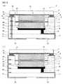
図1(a)は、第1の実施の形態に係る電気二重層キャパシタ1の側面断面図である。電気二重層キャパシタ1は直方体形状を有しており、大きさは、例えば、高さが1[mm]以下、縦が2.5[mm]程度、横が3.0[mm]程度の直方体形状を有している。 FIG. 1A is a side sectional view of the electric
電気二重層キャパシタ1、凹部13を有する凹状容器2、下側の面に金属層15が形成された封口板3(厚さは、0.1[mm]程度)、負極として使用される電極5、正極として使用される電極6、セパレータ7、接合金属層8、金属層11、集電体18、貫通電極21、貫通電極22、端子10、端子12、及び、凹部13に封入された電解質(図示せず)などを用いて構成されている。
端子10、12は、表面実装のための端子であり、以下では、端子10、12の側を下方向、封口板3の側を上方向とする。
なお、図1(a)では、部材の接合関係が分かりやすいように、電極5、セパレータ7、電極6の間に間隙を図示しているが、凹部13にこれらの部材を隙間なく詰め込んでもよい。Electric
The
In FIG. 1A, a gap is illustrated between the
凹状容器2は、例えば、アルミナを用いたセラミックスで構成されており、グリーンシートと呼ばれる柔軟性を有するセラミックスのシート材41〜45を複数枚重ねて焼成して一体化することにより形成される。焼成後の各シートの厚みは100〜300μmとすることが出来る。また、同一の厚みであると、シートを用意する際の管理上の手間が減り望ましい。図1(a)では、シート材41〜45の接合部を破線で示してある。
グリーンシートには、凹部13と貯留部17に対応する開口部と貫通電極21、22を設置する貫通孔に対応する孔が形成されており、これらグリーンシートを厚さ方向に積層して焼成することにより、凹部13と貫通電極21、22用の貫通孔を有する凹状容器2が形成される。ここで、貫通電極の直径は、約100μmとすることが出来る。また、各層に形成された貫通電極と貫通電極が、グリーンシートを積層する際に、ずれた際の誤差を吸収する目的で、各グリーンシートの上面に予めタングステン(W)製の導体印刷を施すことができる。The
The green sheet has openings corresponding to the
より詳細には、シート材41、42には、貫通電極21、22の形状に対応する貫通孔が形成されており、シート材43には、貫通電極21の形状に対応する貫通孔と貯留部17の形状に対応する開口部が形成されており、シート材44〜45には、貫通電極21の形状に対応する貫通孔と凹部13の形状に対応する開口部が形成されている。 More specifically, the
凹部13は、上方から見ると矩形の断面を有しており、凹部13の底部には、底面に金属層11が形成された凹型形状の貯留部17が形成されている。
金属層11は、貯留部17の底面に対応するシート材42の表面に導体印刷し、凹状容器2を焼成することにより形成される。
ここでは、金属層11の大きさを必要最低限としてコストを低減している。なお、貯留部17の底面全体に金属層11を形成してもよい。
導体印刷は、例えば、タングステンなどの耐食性があり、凹状容器2の焼成に耐えうる高融点の金属材料を含むインキでスクリーン印刷することにより行われる。The
The
Here, the size of the
The conductor printing is performed by screen printing with an ink containing a high melting point metal material that has corrosion resistance such as tungsten and can withstand firing of the
タングステンは、融点が高く、また、酸化しにくく、更に、セラミックス面との適度な密着極度を有し、焼成後も実用的な電気抵抗を有するため、凹部13に形成する電極として適している。
しかし、タングステンを正極の集電体として使用する場合、電解質に接した状態で電圧を印加すると電解質中に電気化学的に溶け出す。
そこで、当該溶出を防止するために、次に説明するように電解質に接する全面(即ち、凹状容器2内の部分全て)を導電ペーストによる集電体18で被覆する必要がある。Tungsten is suitable as an electrode to be formed in the
However, when tungsten is used as a positive electrode current collector, when a voltage is applied in contact with the electrolyte, it dissolves electrochemically in the electrolyte.
Therefore, in order to prevent the elution, it is necessary to cover the entire surface in contact with the electrolyte (that is, all the portions in the concave container 2) with the
また、全面に塗布することで、自身の表面張力によって内部側面の壁面にそってメニスカス形状に形成されるものの、液状のペーストの中心部の厚みを平坦化する効果もある。
電気化学的に、電子は、導体の鋭利な先端部に集中する傾向がある。電気化学デバイスを充放電する際に、電子が、この導体の鋭利な先端部に集中すると、その先端部の周囲にのみ、電力が集中し、劣化が促進されることが危惧される。
そこで、本発明のペーストを塗布することで、鋭利部位を無くし、電子の集中を無くすことで、電極の劣化を避けることが期待できる。In addition, by applying to the entire surface, although it is formed in a meniscus shape along the wall surface of the inner side surface by its own surface tension, it also has the effect of flattening the thickness of the central portion of the liquid paste.
Electrochemically, electrons tend to concentrate at the sharp tip of the conductor. When charging / discharging the electrochemical device, if electrons concentrate on the sharp tip of the conductor, there is a concern that power concentrates only around the tip of the conductor and deterioration is accelerated.
Therefore, by applying the paste of the present invention, it can be expected that the sharp portion is eliminated and the concentration of electrons is eliminated, thereby preventing the deterioration of the electrode.
金属層11の上には、導電ペーストを固化した集電体18が形成されている。
金属層11は、厚みを有するが、導電ペーストにより金属層11の厚みが均され、表面が平らな集電体18が得られる。
導電ペーストは、炭素材料と溶媒を含んだフェノール系樹脂をペースト状に加工したものを用いる。炭素材料は、導電性を付与するために添加されている。炭素材料としては、黒鉛の粉末、無定形炭素(カーボンブラック)の何れか、あるいは、両方を混合して用いることができる。
加熱により溶媒を乾燥させてフェノール系樹脂成分を重合(固化)させると、フェノール系の樹脂をバインダーとし、炭素を導電体とする樹脂製の集電体18が形成される。On the
Although the
As the conductive paste, a paste obtained by processing a phenolic resin containing a carbon material and a solvent into a paste is used. The carbon material is added to impart conductivity. As the carbon material, any of graphite powder, amorphous carbon (carbon black), or a mixture of both can be used.
When the solvent is dried by heating to polymerize (solidify) the phenolic resin component, a resin
ここで、一般に負極の集電体の場合、ニッケル、銅、真鍮、亜鉛、スズ、金、ステンレス、タングステン、アルミニウムなど、多くの金属を用いることができるが、正極の集電体は、電解質に集電体が溶け出さないようにするために、アルミニウム、チタン、ニオブなどのプラグメタルと呼ばれる金属を用いる必要がある。正極の集電体としては、これら金属以外では、炭素を用いることができ、本実施の形態では、炭素材を含む導電ペーストを用いることにした。導電ペーストを用いると、プラグメタルの薄膜を真空蒸着などで形成する必要がないため、工程が大幅に簡略化される。 Here, in general, in the case of a negative electrode current collector, many metals such as nickel, copper, brass, zinc, tin, gold, stainless steel, tungsten, and aluminum can be used, but the positive electrode current collector is used as an electrolyte. In order to prevent the current collector from melting, it is necessary to use a metal called plug metal such as aluminum, titanium, or niobium. As the positive electrode current collector, carbon other than these metals can be used, and in this embodiment, a conductive paste containing a carbon material is used. When a conductive paste is used, it is not necessary to form a plug metal thin film by vacuum deposition or the like, so that the process is greatly simplified.
導電ペーストは、カーボン類の中では結晶性の高い黒鉛とカーボン類の中でも無定形のカーボンブラックの2種類を混合し、更に、フェノール系樹脂を主成分と結着剤を含有する。このフェノール系樹脂には、ホルムアルデヒドを代表とするアルデヒドとフェノールを含むその誘導体を用いることができる。 The conductive paste is a mixture of graphite, which is highly crystalline among carbons, and amorphous carbon black among carbons, and further contains a phenolic resin as a main component and a binder. For this phenolic resin, an aldehyde represented by formaldehyde and a derivative containing phenol can be used.
貯留部17は、凹部13の底部の中央に形成され、貯留部17の深さは、電極6の厚さよりも小さく設定されており、貯留部17の内周は、電極6の外周より導電ペーストのメニスカス19の程度大きく設定されている。貯留部17は、導電ペーストが固化する前に飛び散ったり、はみ出したりして短絡の原因となるのを防ぐために設けられている。
貯留部17は、絶縁性のシート材42、43で形成された導電ペーストを保持するための溜め部として機能している。The
The
ここで、メニスカス19は、導電ペーストを貯留部17に貯留した際に、表面張力によって導電ペーストの表面に生じる凹面である。
電気二重層キャパシタ1を製造する際に、貯留部17に液体状の導電ペーストを貯留し、その表面に電極6を置くと、メニスカス19によって電極6が貯留部17の中央に位置決めされる。Here, the
When the electric
その後、加熱して導電ペーストを固化すると、集電体18が形成されると共に電極6が貯留部17の中央に固定される。即ち、電極6が導電ペーストの表面張力によって形成される凹面に固定されるため、電極6を容易かつ正確に位置決めすることができる。
このように、本実施の形態では、正極集電体の形成に真空蒸着などのドライプロセスが必要ないほか、電極6の位置決めも容易なため、電気二重層キャパシタ1の製造コストの低減と生産性の向上を図ることができる。Thereafter, when the conductive paste is solidified by heating, the
As described above, in this embodiment, the formation of the positive electrode current collector does not require a dry process such as vacuum vapor deposition, and the
電極6は、活性炭を主成分とする電極活物質をシート状に形成して矩形に切断することにより形成されており、例えば、天然素材ではヤシガラ、人造材料では、石炭ピッチ、石油ピッチやフェノール系樹脂の炭化物をそれぞれ水蒸気や化学薬品または電気学的に賦活したものが用いられる。 The
凹状容器2の凹部13の下には、先に説明したように孔のあいたシート材41、42を積層することにより、凹部13の底面と凹状容器2の底面に開口部を有する貫通孔が形成されている。
そして、当該貫通孔には、金属層11と端子12を電気的に接続する円柱形状の貫通電極22が形成されている。
貫通電極22の外径と貫通孔の内径は同じに設定されており、貫通電極22と貫通孔の内壁の間には間隙が生じないようになっている。貫通電極は、VIAとも呼ばれる。Under the
A cylindrical through
The outer diameter of the through
貫通電極22の直径は、0.1〜0.3[mm]程度である。また、各シート材の層間に、中間電極28が導体印刷により設けられている。中間電極28により、例えば、貫通孔の精度が十分でなかったり、あるいは、シート材の積層がずれた場合であっても、確実に貫通電極22を形成することができる。なお、後述する貫通電極21の構成も同様である。 The diameter of the through
貫通電極22は、この貫通孔にタングステンなどの金属粉末を主成分とする金属ペーストを焼結させたり、カーボン等の導電ペーストを注入して固化させたり、あるいは、金属製の棒材や板材を挿入することにより形成される。金属製の棒材としては、例えば、アルミニウム、ステンレススチール、タングステン、ニッケル、銀、金、あるいは、炭素を含む導電性樹脂などを用いることができる。電極6は、金属層11、貫通電極22を介して端子12に電気的に接続している。 The through
凹部13の開口部の端部には、封口板3と凹状容器2を接合する金属層である金属層9と接合金属層8が形成されている。
接合金属層8は、開口部の端部の全周に形成された金属層9(メタライズ層)の上に形成されたろう材(ニッケル、金など)の層から構成されている。接合金属層8は、封口板3と凹状容器2の間の気密性を確保するためシールリングと呼ばれることもある。A
The
メタライズ層は、例えば、コバール(Co:17、Ni:29、Fe:54の比率の合金)で構成されており、コバール製の金属リングを凹状容器2の端部に設置して焼成することにより形成される。
後述するように、封口板3を凹部13の開口部に設置して加熱すると、ろう材の層が溶けて金属層15と融着し、凹部13が封口板3により封口される。The metallized layer is made of, for example, kovar (alloy of ratio of Co: 17, Ni: 29, Fe: 54), and a metal ring made of Kovar is placed on the end of the
As will be described later, when the sealing plate 3 is placed in the opening of the
凹状容器2には、孔をあけたシート材41〜45を積層することにより、凹部13を囲む側壁内に、凹部13の開口部の端部と凹状容器2の底面に開口部を有する貫通孔が形成されている。
そして、当該貫通孔には、接合金属層8と端子10を電気的に接続する円柱形状の貫通電極21が形成されている。
貫通電極21の外径と貫通孔の内径は同じに設定されており、貫通電極21と貫通孔の内壁の間には間隙が生じないようになっている。
貫通電極21の材質や形成方法、及び中間電極28を用いて接合することなどは貫通電極22と同様である。In the
A cylindrical through
The outer diameter of the through
The material and forming method of the through
端子10、12は、タングステンを含むインキなどで導体印刷して焼成した後、その表面に金やニッケルなどをメッキして形成されている。更に、ニッケルメッキの上に、防錆のため金やスズ等の金属をメッキすることが出来る。
メッキには、電解メッキ、無電解メッキなどがあり、また、真空蒸着などの気相法によって形成してもよい。
これにより、端子10、12の高いハンダ濡れ性が確保され、電気二重層キャパシタ1を基板に良好に表面実装することができる。
なお、本実施の形態では、端子10、12を凹状容器2の外側底面部に設けたが、外側側面部に形成したり、あるいは、外側底面から側面に連続して形成してもよい。
端子10、12は、貫通孔に貫通電極21、22を設置した後に形成する。
また、端子10、12を凹状容器2の底部の端部まで形成しないようにすると、大判のシート材で電気二重層キャパシタ1を同時に多数形成する場合に、これらを切り分けするときに端子10、12の剥がれなどを防止することができる。The
The plating includes electrolytic plating and electroless plating, and may be formed by a vapor phase method such as vacuum deposition.
Thereby, the high solder wettability of the
In addition, in this Embodiment, although the
The
Further, if the
封口板3は、コバールなどで構成された金属部材である。コバールは、セラミックスと熱膨張率がおおよそ等しいため、リフロー時に電気二重層キャパシタ1を加熱した場合に封口板3と凹状容器2の間に発生する応力を抑制することができる。
封口板3の下側の面には、封口板3を接合金属層8に良好に接合するために、ニッケルメッキによる金属層15が形成されている。
金属層15が接合金属層8にろう付けされると封口板3が凹部13の開口部に物理的、及び電気的に接合する。The sealing plate 3 is a metal member made of Kovar or the like. Since Kovar has a thermal expansion coefficient approximately equal to that of ceramics, it is possible to suppress the stress generated between the sealing plate 3 and the
On the lower surface of the sealing plate 3, a
When the
ろう付けは、封口板3を加圧しながら加熱することにより溶解し、封口板3と凹状容器2を接合する。
より具体的には、ローラ電極を封口板3の縁部に適当な圧力で接触させ、通電しながら回転走行させるパラレルシーム溶接を用いることができる。接触抵抗により接合金属層8が加熱され、加圧と加熱が行われる。パラレルシーム溶接以外にも、レーザーによる加熱溶接も可能である。The brazing is dissolved by heating the sealing plate 3 while applying pressure, and the sealing plate 3 and the
More specifically, it is possible to use parallel seam welding in which the roller electrode is brought into contact with the edge of the sealing plate 3 with an appropriate pressure and is rotated while being energized. The
パラレルシーム溶接を行う場合、接合金属層8と封口板3の相性がよい材料を選択するのが望ましく、例えば、接合金属層8に電解ニッケル、無電解ニッケルを用いた場合は、封口板3は、コバールに電解ニッケル、または無電解ニッケルを施したものを用いる。
または、その逆に、接合金属層8に電解ニッケルを用いた場合は、封口板3は、コバールに無電解ニッケルを施したものを用いる。これにより、必要以上に溶接パワーを上げなくて済む。更に、無電解ニッケルを行う場合は、各種還元剤を用いることができる。例えば、ジメチルアミンボラン、次亜リン酸、ヒドラジン、水素化ホウ素ナトリウムなどが挙げられる。ここで、ろう材として、メッキに用いたニッケルを溶融させる際、ニッケルの融点が低い方が望ましい。そこで、メッキの際の還元剤には次亜リン酸を用いることで、仕上がったメッキの化学組成が、「Ni:90%-96%、P:4%-10%」である場合に、ホウ素を含有する場合に比較して、融点が低いので、ろう付けに適する。
また、接合金属層8のシールリングをセラミックスのメタライズ層に固着させるためには、金ろう、銀ろうなどのろう材やハンダ材を用いることも可能である。When performing parallel seam welding, it is desirable to select a material with good compatibility between the
Or, conversely, when electrolytic nickel is used for the
Further, in order to fix the seal ring of the
金属層15の下側の表面には、電極活物質で構成された電極5が炭素を含有する導電性接着剤により接合している。
電極5の材質と形状は電極6と同様である。金属層15のうち電極5と接している部分51は、集電体として機能する。そして、金属層15のうち電極5と接していない部分52は、集電体と接合する導電体として機能している。
このようにして、電極5は、金属層15、接合金属層8、貫通電極21を介して端子10に電気的に接続している。An
The material and shape of the
In this way, the
電極5、6は、凹部13と封口板3により構成される空洞部内で対面しており、電極5、6の間には、電極5、6の接触による短絡を防止するためのセパレータ7が設置されている。
セパレータ7の材質としては、例えば、PPS(ポリフェニレンサルファイド)、PEEK(ポリエーテルエーテルケトン)、変性PEEK、PTFE(ポリテトラフルオロエチレン)などの耐熱性樹脂などの表面に親水性を付与した材料からなる不織布、またはガラス繊維を用いることができる。The
The material of the
更に、凹部13と封口板3より構成される空洞部内には電解質が封入されている。
電解質は、例えば、PC(プロピレンカーボネート)やSL(スルホラン)などの非水溶媒に(CH3)・(CH4)3N・BF4などの支持塩を溶かした溶液で構成されている。このように本実施の形態では支持塩として液体を用いるが、ゲル状や固体状の電解質を用いることも可能である。封止方法にも依存するが、電解質として、液体の溶媒を用いる場合は、沸点が200℃以上あることが望ましい。更に、封口時に印加された熱によって蒸気圧が上がらないことが望ましい。電解液中に沸点が100℃未満の低沸点の溶媒を添加することはできるが、少なくとも樹脂の融点における蒸気圧が0.2MPa−G以下が望ましい。電解液を注入する場合、電解液を凹部13に注液後、減圧や加熱や加圧を単独又は組み合わせることによって、電解質を電極の細部にまで含浸させることができる。
なお、固体の電解質を用いる場合、セパレータ7は不要となる。
更に、固定の電解質を用いる場合、電解質と集電体が接しないように構成すると、集電体が溶け出すことはないため、電極5を正極、電極6を負極とすることも可能である。Further, an electrolyte is enclosed in a hollow portion constituted by the
The electrolyte is composed of a solution in which a supporting salt such as (CH3). (CH4) 3N.BF4 is dissolved in a nonaqueous solvent such as PC (propylene carbonate) or SL (sulfolane). Thus, although a liquid is used as the supporting salt in the present embodiment, a gel-like or solid electrolyte can also be used. Although depending on the sealing method, when a liquid solvent is used as the electrolyte, the boiling point is desirably 200 ° C. or higher. Furthermore, it is desirable that the vapor pressure does not increase due to the heat applied during sealing. A low boiling point solvent having a boiling point of less than 100 ° C. can be added to the electrolytic solution, but at least the vapor pressure at the melting point of the resin is preferably 0.2 MPa-G or less. When injecting an electrolytic solution, the electrolyte can be impregnated into the details of the electrode by injecting the electrolytic solution into the
In addition, when using a solid electrolyte, the
Further, when a fixed electrolyte is used, the current collector is not melted out if the electrolyte and the current collector are not in contact with each other. Therefore, the
以上のように構成された電気二重層キャパシタ1を、端子10を負極、端子12を正極として基板に表面実装し、例えば、携帯電話のメモリやクロックのバックアップ電源として使用することができる。
この場合、携帯電話は、主電源の電池を装着すると同時に電気二重層キャパシタ1を充電しておき、電池交換時や主電源の電圧が低下した場合に、電気二重層キャパシタ1に蓄積された電荷を放電してメモリに電力を供給したり、クロック等の機能を保持する。The electric
In this case, the mobile phone charges the electric
以上では、凹状容器2をアルミナを主成分とするセラミックスで構成したが、例えば、耐熱性樹脂、ガラス、セラミックスガラスなどの耐熱材料で構成することも可能である。
凹状容器2をガラスやガラスセラミックスで形成する場合は、低融点のガラスやガラスセラミックスに導体印刷により配線を施し、積層した後、低温で焼成する。
凹状容器2を樹脂で構成する場合、貫通電極21、22をインサート成型することも可能である。In the above description, the
When the
When the
また、貫通電極22について、シート材42での直径をシート材41での直径よりも大きく設定すると、リフロー時に加熱して凹部13の圧力が上昇した場合であっても、当該圧力が貫通電極22に作用し、貫通電極22が凹状容器2から抜け落ちることを防止することができる。
同様に、貫通電極21について、シート材45での直径をシート材41〜44での直径よりも大きく設定することもできる。Further, if the diameter of the
Similarly, the through
図1(b)は、電気二重層キャパシタ1の変形例を説明するための図である。
この例では、電気二重層キャパシタ1は、貫通電極21、22を有さず、凹状容器2の側面に形成した配線によって電極5、6を端子10、12に接続している。他の構成は、先に説明した第1の実施の形態と同様である。
金属層11は、貯留部17の底面からシート材42の表面に沿って凹状容器2の外部に貫通し、凹状容器2の側面を経て、凹状容器2の底面に形成された端子12に電気的に接続している。FIG. 1B is a diagram for explaining a modification of the electric
In this example, the electric
The
金属層11は、貯留部17の底面において必要最低限の大きさに形成されているが、底面全体に形成してもよい。なお、導電ペーストにより金属層11の厚みが均され、平らな集電体18が得られる。
金属層9は、凹状容器2の上端面で接合金属層8に接合すると共に、凹状容器2の側面を経て、凹状容器2の底面に形成された端子10に電気的に接続している。
凹状容器2の側面では、シート材41〜44の上面に補助電極が設けてあり、側面での電気的接続がより確実となるようにしている。
このように、貫通電極を用いない方式で電気二重層キャパシタ1を構成することもできる。The
The
On the side surface of the
Thus, the electric
図1(c)は、金属層11の上面に、予め導電ペーストを塗布し、固化した集電体20を設置した例である。この場合、導電性接着剤などを用いて、金属層11と集電体20、及び、集電体20と電極6を接合する。
このように、貯留部17に導電ペーストを注入して固化するのではなく、予め固化した導電ペーストを貯留部17に設置してもよい。
なお、集電体20は、金属層11の周囲を隙間無く埋めており、電解液が金属層11に触れないようになっている。
これによって、金属層11が溶出して品質が低下するのを防ぐことができる。FIG. 1C is an example in which a
Thus, instead of injecting and solidifying the conductive paste into the
The
Thereby, it can prevent that the
図2(d)は、貫通電極を導電ペーストで形成した例である。
シート材42に、貯留部17の底面から金属層11に至る貫通孔を形成しておき、貯留部17に導電ペーストを注入すると、導電ペーストが貫通孔に侵入して固化し、貫通電極61が形成される。
また、導電ペーストの注入後、減圧することにより、貫通電極61の位置にペーストと一緒に巻き込んだ気泡を脱泡することができる。
集電体18と貫通電極61は、一体形成されるため、電極6は、集電体18、貫通電極61、金属層11を経由して端子12に電気的に接続する。
また、この例では、接合金属層8と端子10は、貫通電極21により電気的に接続している。
図2(e)は、集電体18と金属層11との電気的接続を貫通電極61で行うとともに、接合金属層8と端子10を金属層9で電気的に接続した例である。FIG. 2D shows an example in which the through electrode is formed of a conductive paste.
When a through hole extending from the bottom surface of the
Further, by reducing the pressure after injecting the conductive paste, bubbles entrained together with the paste at the position of the through
Since the
In this example, the
FIG. 2E shows an example in which the
図3(f)は、凹部13に段部を作らずに、そのまま貯留部17とした例である。この例では、集電体18と金属層11を貫通電極61により電気的に接続している。
図3(g)は、貯留部17の底部の一部に集電体18を形成した例である。このように、貯留部17の底面全面に集電体18を形成しなくても電極6を機能させることができる。
この例では、凹部13に段部を作らずに貯留部17とし、また、貫通電極61により集電体18と金属層11を電気的に接続している。FIG. 3F shows an example in which the
FIG. 3G shows an example in which a
In this example, the
図4の各図は、集電体18の形成方法を説明するための図である。
まず、図4(a)に示したように、接合金属層8、貫通電極21、22、金属層11、端子10、12が形成された凹状容器2を用意する。
そして、貯留部17に集電体18となる導電ペーストを供給する。導電ペーストの供給量は、貯留部17の底面の全てを満たし、メニスカス19が形成される程度に設定されている。Each drawing in FIG. 4 is a diagram for explaining a method of forming the
First, as shown in FIG. 4A, the
And the electrically conductive paste used as the
図4(b)は、貯留部17に導電ペーストを供給する前に凹状容器2を上方から見た図である。
図に示したように、貯留部17の底部には、金属層11が円形に形成されている。なお、金属層11の形状は矩形など任意でよい。
図4(c)は、凹状容器2に導電ペーストを供給したところを上方から見た図である。凹状容器2の中央に集電体18となる導電ペーストが貯留されている。FIG. 4B is a view of the
As shown in the figure, the
FIG. 4C is a view of the conductive paste supplied to the
次に、図5に示したように、集電体18となる導電ペーストの液面に電極6を置く。すると、導電ペーストのメニスカス19によって電極6が貯留部17の中央部に位置する。
そして、180[℃]程度の温度に加熱すると、導電ペーストが固化して集電体18となり、電極6が貯留部17の中央部の固定される。
図示しないが、その後、電極6の上にセパレータ7を置き、電解質を供給して、更に、凹部13の開口部を電極5が取り付けられた封口板3で封口してろう付けすると電気二重層キャパシタ1が完成する。Next, as shown in FIG. 5, the
When heated to a temperature of about 180 [° C.], the conductive paste is solidified to become the
Although not shown in the drawing, when the
なお、導電ペーストを貯留部17に供給して固化させる工程を複数回行って(即ち、複数回に分けて塗布することで)、集電体18を層状に形成することもできる。
この場合、貯留部17に導電ペーストを供給して加熱して固化し、その上に更に導電ペーストを供給して加熱して固化する工程を、最上層の下の層まで繰り返す。
そして、最上の層を形成する際は、最上層となる導電ペーストを供給して、その液面に電極6を設置してから加熱して最上層の導電ペーストを固化させる。このようにして、集電体18は、層状に形成される。The
In this case, the process of supplying the conductive paste to the
When the uppermost layer is formed, the uppermost conductive paste is supplied by supplying the uppermost conductive paste, and the
また、導電性のペーストの厚みが薄い場合においても、導電ペーストの厚みの差や分布によって、電気抵抗にバラツキが生じるため、程度は低いが、電力の集中が起こる。
そのため、導電ペーストを塗布する際は、概ね50μm以上の均一な厚みに塗布することが重要である。塗布後、加熱することで、ペーストに含まれる硬化成分の主剤と固化の促進剤が化学反応によって、重合し、カーボン同士が接触することで電子導電性のネットワークを有する集電体層18が形成される。Even when the thickness of the conductive paste is thin, the electric resistance varies due to the difference or distribution of the thickness of the conductive paste, and thus the power concentration occurs to a small extent.
Therefore, when applying the conductive paste, it is important to apply a uniform thickness of approximately 50 μm or more. By heating after application, the main component of the curing component and the solidification accelerator contained in the paste are polymerized by a chemical reaction, and the
そのとき、導電ペーストの粘度を下げる目的で、有機溶媒を加えることがあり、その溶媒が気化する際に気泡を生じ、直径数μm程度の小径な連通孔を形成することがある。
または、導電ペーストの塗布時に巻き込んだ雰囲気の中のガス成分をも上述の小径な連通孔を形成することがある。この連通孔を介して、電解質が金属層11と接する場合、その連通孔から金属層11の金属が溶出し、活性炭の表面で、還元され金属となる場合がある。
このような金属の溶解と析出を回避するため、導電ペーストの塗布後、減圧することより、気泡を脱泡することで、前出の連通孔の生成を抑制するという効果を得ることができる。
また、導電ペーストは複数回に分けて、概ね50μm以上の均一な厚みに塗布することでも、前出の連通孔の生成を抑制するという効果を得ることができる。この時、少なくとも、2回以上に分けて塗布することがよく、より望ましくは、3回以上の塗布が望ましい。At that time, an organic solvent may be added for the purpose of lowering the viscosity of the conductive paste, and when the solvent is vaporized, bubbles are formed, and a small communication hole having a diameter of about several μm may be formed.
Alternatively, the above-described small-diameter communication holes may also be formed by the gas component in the atmosphere entrained when the conductive paste is applied. When the electrolyte is in contact with the
In order to avoid such dissolution and precipitation of the metal, it is possible to obtain the effect of suppressing the generation of the above-mentioned communication holes by defoaming the bubbles by applying a reduced pressure after applying the conductive paste.
Also, the conductive paste can be divided into a plurality of times and applied to a uniform thickness of approximately 50 μm or more to obtain the effect of suppressing the formation of the above-described communication holes. At this time, it is preferable to apply at least two times, and more preferably three times or more.
以上に説明した実施の形態により、次のような効果を得ることができる。
(1)炭素材で正極の集電体18を形成することができる。
(2)導電ペーストを固化させて集電体18を形成するため真空蒸着などのドライプロセスが必要ない。
(3)凹部13の底部に貯留部17を設けることにより、液体状の導電ペーストを貯留することができ、導電ペーストのはみ出しなどを防止することができる。
(4)貯留した液体状の導電ペーストの上に電極6を置くことにより、電極6を導電ペーストの表面張力によって容易に位置決めすることができる。According to the embodiment described above, the following effects can be obtained.
(1) The positive electrode
(2) Since the conductive paste is solidified to form the
(3) By providing the
(4) By placing the
(第2の実施の形態)
図6(a)は、第2の実施の形態に係る電気二重層キャパシタ1の側面断面図である。
第1の実施の形態と同じ構成要素には同じ符号を付し、説明を省略する。
凹部13の底面には、当該底面を二分する突起部33が形成されている。そして、凹部13の底面には、突起部33によって、固化する前の導電ペーストを貯留する溜め部である2つの貯留部17a、17bが形成されている。
貯留部17a、17bで固化した導電ペーストがそれぞれ、集電体18a、18bとなる。なお、使用する導電ペーストは、第1の実施の形態と同様である。(Second Embodiment)
FIG. 6A is a side sectional view of the electric
The same components as those in the first embodiment are denoted by the same reference numerals, and description thereof is omitted.
A
The conductive paste solidified in the
貯留部17a、17bの深さは、導電ペーストが溜められる程度であり、貯留部17a、17bの内周は、電極5、6の外周より導電ペーストのメニスカスの程度大きく設定されている。 The depths of the
貯留部17a、17bの底面には、それぞれ、金属層11a、11bが形成されている。金属層11a、11bの製法は、第1の実施の形態の金属層11と同様である。
貯留部17a、17bは、それぞれ、凹状容器2の底部に形成された貫通電極21、22によって、端子10、12に電気的に接続している。貫通電極21、22は、中間電極28によって確実に接合する。Metal layers 11a and 11b are formed on the bottom surfaces of the
The
貯留部17a、17bでは、それぞれ、金属層11a、11bの上側の面に、導電ペーストを固化した集電体18a、18bの層が形成されており、更に、その上に電極5、6が呈されている。
これは、導電ペーストが液体のときに、その上に、電極5、6を置いて、導電ペーストを加熱・固化させて電極5、電極6を集電体18a、18bによって貯留部17a、17bに固定したものである。
金属層11a、11bは、必要最小限の面積に形成されており、その厚さが導電ペーストによって均されて、集電体18a、18bの上面は平らになっている。なお、金属層11a、11bは、貯留部17a、17bの底面全体に形成してもよい。In the
This is because when the conductive paste is liquid, the
The metal layers 11a and 11b are formed in a necessary minimum area, the thickness thereof is leveled by the conductive paste, and the upper surfaces of the
電極5、6は、直方体形状を有しており、第1の実施の形態の電極5、6と同じ材質で構成されている。なお、電極5、6を円柱形状など、他の形状とすることも可能である。
第2の実施の形態では、電極5、6が対称的に形成されているため、何れを正極としてもよい。
また、電極5、6は、突起部33の上部で対面しており、電極5、6の間には短絡を防止するセパレータ7が配置されている。セパレータ7の材質は第1の実施の形態と同様である。なお、個体の電解質を用いる場合、セパレータ7は不要となる。The
In the second embodiment, since the
Further, the
凹部13は、電解質が満たされており、電極5、6の上側の面と封口板3の下側の面(金属層15の表面)の間には、当該電解質を含浸した含浸部材31が設置されている。
含浸部材31は、ガラス材や樹脂ウィックなどからスポンジ状に形成されており、弾性及び吸液性を有している。
含浸部材31は、電極5、6、及びセパレータ7に押圧されている。これによって、含浸部材31は、電極5、6が電解質に接した状態で、電極5、6、及びセパレータ7を保持することができる。The
The impregnating
The
封口板3の構成は、第1の実施の形態と同様であるが、例えば、封口板3をアルミニウムで形成し、熱酸化処理によって、下側の面にアルミナによる絶縁層を形成したものを用いてもよい。これにより、衝撃などにより、電極5、6が封口板3の下側の面に接した場合でも短絡を防ぐことができる。 The structure of the sealing plate 3 is the same as that of the first embodiment. For example, the sealing plate 3 is made of aluminum and an insulating layer made of alumina is formed on the lower surface by thermal oxidation. May be. Thereby, even when the
凹状容器2は、第1の実施の形態と同様にグリーンシートによるシート材41〜45を積層して形成されている。
シート材41、42には、貫通電極21、22を形成する貫通孔が形成されており、シート材43〜45には、凹部13に対応する開口部が形成されている。シート材43には、突起部33となる部分が抜かれずに残っている。The
Through holes for forming the through
図6(b)は、第2の実施の形態の変形例を説明するための図である。
この例では、電気二重層キャパシタ1は、貫通電極21、22を有さず、凹状容器2の側面に形成した配線によって電極5、6を端子10、12に接続している。他の構成は、先に説明した第2の実施の形態と同様である。
金属層11a、11bは、それぞれ、貯留部17a、17bの底面からシート材42の表面に沿って凹状容器2の外部に貫通し、凹状容器2の側面を経て、端子10、12に電気的に接続している。金属層11a、11bは、貯留部17a、17bの底面に必要最小限の大きさで形成されているが、底面全体に形成してもよい。
このように、貫通電極を用いない方式で電気二重層キャパシタ1を構成することもできる。FIG. 6B is a diagram for explaining a modification of the second embodiment.
In this example, the electric
The metal layers 11a and 11b penetrate the outside of the
Thus, the electric
図7(a)は、第2の実施の形態の更なる変形例を説明するための図である。
凹状容器2は、樹脂製のシート材41〜45を形成して構成されている。
樹脂としては、例えば、PTFE(テトラフルオロエチレン)、PFA(ポリテトラフルオロエチレン)、FRP(繊維強化プラスチック)などを用いることができる。
PFAは、ステンレスと溶着し、PTFEは、強度が高いなど、樹脂に特有の性質があるため、例えば、シート材41をPTFE、シート材42、43をPFA、シート材44、45をPTFEにするといったように、異種の樹脂のシート材を組み合わせることができる。FIG. 7A is a diagram for explaining a further modification of the second embodiment.
The
As the resin, for example, PTFE (tetrafluoroethylene), PFA (polytetrafluoroethylene), FRP (fiber reinforced plastic), or the like can be used.
PFA is welded to stainless steel and PTFE has high properties such as high strength. Therefore, for example, the
金属層11a、11bは、例えば、ステンレススチールの板材を用いて形成されており、シート材41〜45と共に積層・加熱され、シート材42、43に溶着する。
金属層11a、11bは、凹状容器2の底面に曲げられて、金属層11a、11bの先端部分が端子10、12を形成する。
封口板3は、例えば、PTFEのシート材により構成され、レーザ溶接などにより、凹状容器2の開口部に溶着している。
金属層11a、11bの厚みは、導電ペーストにより均され、集電体18a、18bの上面は平らとなる。導電ペーストは多重塗装してもよい。
金属層11a、11bとして金属板を用いるとコストを低減することができる。The metal layers 11 a and 11 b are formed using, for example, a stainless steel plate material, and are laminated and heated together with the
The metal layers 11a and 11b are bent to the bottom surface of the
The sealing plate 3 is made of, for example, a PTFE sheet material, and is welded to the opening of the
The thickness of the
If metal plates are used as the
図7(b)は、第2の実施の形態の更なる変形例を説明するための図である。
この例では、集電体18aと金属層11a、及び、集電体18bと金属層11bが、それぞれ、導電ペーストを固化して形成された貫通電極61a、61bにより電気的に接続されている。FIG.7 (b) is a figure for demonstrating the further modification of 2nd Embodiment.
In this example, the
図8の各図は、集電体18a、18bの形成方法を説明するための図である。
まず、図8(a)に示したように、接合金属層8、貫通電極21、22、貯留部17a、17b、金属層11a、11b、端子10、12が形成された凹状容器2を用意する。
そして、貯留部17a、17bに導電ペーストを供給する。導電ペーストの供給量は、貯留部17a、17bの底面の全てを満たし、メニスカス19a、19bが形成される程度に設定されている。
図8(b)は、凹状容器2に導電ペーストを供給したところを上方から見たところを示している。貯留部17a、17bに固化すると集電体18a、18bとなる導電ペーストが貯留されている。Each figure of FIG. 8 is a figure for demonstrating the formation method of
First, as shown in FIG. 8 (a), a
And the electrically conductive paste is supplied to the
FIG. 8B shows a place where the conductive paste is supplied to the
次に、図8(c)に示したように、導電ペーストの液面に、それぞれ、電極5、6を置く。すると、導電ペーストのメニスカスによって、電極5、6が、それぞれ貯留部17a、17bの中央部に位置する。
そして、180[℃]程度の温度に加熱すると、導電ペーストが固化し、導電ペーストが固化して集電体18a、18bとなり、電極5、6が貯留部17a、17bの中央部に固定される。
図示しないが、その後、電極5、6の間にセパレータ7を置き、電解質を供給する。更に、電解質を含浸した含浸部材31を電極5、6の上において、凹部13の開口部を封口板3で封口してろう付けすると電気二重層キャパシタ1が完成する。Next, as shown in FIG. 8C,
When heated to a temperature of about 180 [° C.], the conductive paste is solidified, the conductive paste is solidified to become
Although not shown, a
以上に説明した第1の実施の形態により、次の構成を得ることができる。
封口板3で封口された凹状容器2は、凹部13が空洞部となるため、空洞部を有する容器として機能している。
金属層11及びこれに接合した貫通電極22は、前記空洞部から前記容器の外部に導通する第1の導電体として機能している。
集電体18は、前記空洞部内で前記第1の導電体と接合し、炭素を導電材とする第1の集電体として機能している。
電極6は、前記第1の集電体に接合する第1の電極として機能している。
金属層15の電極5と接しない部分52、及びこれと接合する接合金属層8、貫通電極21は、前記空洞部から前記容器の外部に導通する第2の導電体として機能している。
金属層15の電極5と接する部分51は、前記空洞部内で前記第2の導電体と接合する第2の集電体として機能している。
電極5は、前記第2の集電体に接合し、前記第1の電極と所定距離を隔てて面する第2の電極として機能している。
凹部13に封入される電解質は、前記第1の電極、及び第2の電極に接する電解質として機能している。According to the first embodiment described above, the following configuration can be obtained.
The
The
The
The
The
The
The
The electrolyte sealed in the
電極6は、正極として使用され、電極5は、負極として使用されるため、前記第1の電極は正極であり、前記第2の電極は負極となっている。 Since the
金属層11が電解質に溶解するのを防止するために凹部13内において金属層11は全て集電体18に覆われているため、前記第1の集電体は、前記空洞部内で前記第1の導電体の全てを被覆している。 In order to prevent the
導電ペーストは、炭素材料と溶媒を含んだフェノール系樹脂をペースト状に加工したものが用いられ、フェノール系樹脂成分を重合して樹脂状となるため、前記第1の集電体は、炭素を導電材とする樹脂によって形成されている。 The conductive paste is a paste obtained by processing a phenolic resin containing a carbon material and a solvent into a paste, and since the phenolic resin component is polymerized into a resinous form, the first current collector contains carbon. It is made of a resin used as a conductive material.
集電体18は、貯留部17(凹部で形成されている)に形成されているため、前記第1の集電体は、前記空洞部に形成された凹部に形成されている。 Since the
導電ペーストの供給と固化を繰り返すことにより集電体18を層状に形成することができ、この場合、前記第1の集電体は、炭素を導電材とする部材が層状に形成されている。 By repeating the supply and solidification of the conductive paste, the
また、第2の実施の形態では、電極5に対しても導電ペーストで集電体を形成するため、この場合、前記第2の集電体は、炭素を導電材としている。 In the second embodiment, since the current collector is also formed on the
また、電気二重層キャパシタ1は、例えば、携帯電話のメモリやクロックのバックアップ電源として使用することができる。
この場合、当該携帯電話は、電気二重層キャパシタ1で構成された電子部品と、主電源の電池を装着すると同時に前記電子部品に蓄電する蓄電手段と、メモリやクロックなどの所定の機能を発揮するほかの電子部品と、蓄電した電荷を放電してメモリやクロックに電力を供給するなど、前記蓄電した電荷を用いて前記他の電子部品に電力を供給する電力供給手段を備えた電子装置として機能している。The electric
In this case, the cellular phone exhibits predetermined functions such as an electronic component composed of the electric
凹状容器2は、シート材41〜45を積層して形成されており、空洞を形成するための凹部13、貯留部17、金属層11、貫通電極21、22が形成されているため、電気二重層キャパシタ1の製造工程は、空洞を形成するための凹部と、前記凹部内に形成された導電ペーストを貯留する貯留部と、前記貯留部の底面から外部に導通する第1の導電体と、を有する凹状容器を形成するステップを有している。
また、貯留部17に導電ペーストを供給して液面に電極6を設置し、その後、加熱して導電ペーストを固化させるため、当該製造工程は、前記貯留部に炭素を導電材とする導電ペーストを供給するステップと、前記供給した導電ペーストの上に第1の電極を設置するステップと、前記第1の電極が設置された導電ペーストを固化させて第1の集電体を形成するステップを有している。
更に、金属層15に電極5を接合し、凹部13に電解質を供給してセパレータ7と共に電極5を凹部13に設置するため、当該工程は、前記凹部に、第2の集電体と、前記第2の集電体に設置され、前記第1の電極と所定距離を隔てて対面する第2の電極と、前記第2の集電体に接合し、外部に導通する第2の導電体と、前記第1の電極、及び前記第2の電極に接する電解質と、を形成するステップを有している。
ろう付けして凹部13を封口板3で封口するため、当該工程は、前記凹部を封口するステップを有している。The
In addition, in order to supply the conductive paste to the
Further, the
Since the
1 電気二重層キャパシタ
2 凹状容器
3 封口板
5 電極
6 電極
7 セパレータ
8 接合金属層
9 金属層
10 端子
11 金属層
12 端子
13 凹部
15 金属層
17 貯留部
18 集電体
19 メニスカス
21、22 貫通電極
28 中間電極
31 含浸部材
33 突起部
41〜45 シート材
51、52 部分
61 貫通電極
100 電気二重層キャパシタ
102 凹状容器
103 封口板
105 負極電極
106 正極電極
107 セパレータ
108 接合金属層
109 金属層
110 負極端子
111 金属層
112 正極端子
113 凹部
115 金属層DESCRIPTION OF
Claims (9)
Translated fromJapanese前記空洞部から前記容器の外部に導通する第1の導電体と、
前記空洞部内で前記第1の導電体と接合し、炭素を導電材とする第1の集電体と、
前記第1の集電体に接合する第1の電極と、
前記空洞部から前記容器の外部に導通する第2の導電体と、
前記空洞部内で前記第2の導電体と接合する第2の集電体と、
前記第2の集電体に接合し、前記第1の電極と所定距離を隔てて面する第2の電極と、
前記第1の電極、及び第2の電極に接する電解質と、
を具備したことを特徴とする電子部品。A container having a cavity,
A first conductor that conducts from the cavity to the outside of the container;
A first current collector bonded to the first conductor in the cavity and using carbon as a conductive material;
A first electrode joined to the first current collector;
A second conductor that conducts from the cavity to the outside of the container;
A second current collector joined to the second conductor in the cavity;
A second electrode joined to the second current collector and facing the first electrode at a predetermined distance;
An electrolyte in contact with the first electrode and the second electrode;
An electronic component comprising:
前記電子部品に蓄電する蓄電手段と、
所定の機能を発揮する他の電子部品と、
前記蓄電した電荷を用いて前記他の電子部品に電力を供給する電力供給手段と、
を具備したことを特徴とする電子装置。An electronic component according to any one of claims 1 to 7, and
Power storage means for storing power in the electronic component;
With other electronic components that perform the specified function,
Power supply means for supplying power to the other electronic component using the stored charge;
An electronic device comprising:
前記貯留部に炭素を導電材とする導電ペーストを供給するステップと、
前記供給した導電ペーストの上に第1の電極を設置するステップと、
前記第1の電極が設置された導電ペーストを固化させて第1の集電体を形成するステップと、
前記凹部に、第2の集電体と、前記第2の集電体に設置され、前記第1の電極と所定距離を隔てて対面する第2の電極と、前記第2の集電体に接合し、外部に導通する第2の導電体と、前記第1の電極、及び前記第2の電極に接する電解質と、を形成するステップと、
前記凹部を封口するステップと、
を含むことを特徴とする電子部品の製造方法。Forming a concave container having a concave portion for forming a cavity, a storage portion for storing the conductive paste formed in the concave portion, and a first conductor that conducts from the bottom surface of the storage portion to the outside. When,
Supplying a conductive paste containing carbon as a conductive material to the reservoir;
Installing a first electrode on the supplied conductive paste;
Solidifying the conductive paste provided with the first electrode to form a first current collector;
In the recess, a second current collector, a second electrode installed on the second current collector and facing the first electrode with a predetermined distance, and the second current collector Forming a second conductor that joins and conducts to the outside, the first electrode, and the electrolyte in contact with the second electrode;
Sealing the recess;
The manufacturing method of the electronic component characterized by including.
Priority Applications (3)
| Application Number | Priority Date | Filing Date | Title |
|---|---|---|---|
| JP2010185739AJP5777001B2 (en) | 2010-08-23 | 2010-08-23 | Electronic component, electronic device, and method of manufacturing electronic component |
| CN201510354013.3ACN105185603B (en) | 2010-08-23 | 2011-08-19 | Electronic unit and electronic installation |
| CN201110240090.8ACN102376458B (en) | 2010-08-23 | 2011-08-19 | Electronic component, electronic device, and method for manufacturing electronic component |
Applications Claiming Priority (1)
| Application Number | Priority Date | Filing Date | Title |
|---|---|---|---|
| JP2010185739AJP5777001B2 (en) | 2010-08-23 | 2010-08-23 | Electronic component, electronic device, and method of manufacturing electronic component |
Related Child Applications (1)
| Application Number | Title | Priority Date | Filing Date |
|---|---|---|---|
| JP2014262446ADivisionJP6032684B2 (en) | 2014-12-25 | 2014-12-25 | Electronic component and electronic device |
Publications (2)
| Publication Number | Publication Date |
|---|---|
| JP2012044074Atrue JP2012044074A (en) | 2012-03-01 |
| JP5777001B2 JP5777001B2 (en) | 2015-09-09 |
Family
ID=45794901
Family Applications (1)
| Application Number | Title | Priority Date | Filing Date |
|---|---|---|---|
| JP2010185739AActiveJP5777001B2 (en) | 2010-08-23 | 2010-08-23 | Electronic component, electronic device, and method of manufacturing electronic component |
Country Status (2)
| Country | Link |
|---|---|
| JP (1) | JP5777001B2 (en) |
| CN (2) | CN102376458B (en) |
Cited By (18)
| Publication number | Priority date | Publication date | Assignee | Title |
|---|---|---|---|---|
| JP2012227333A (en)* | 2011-04-19 | 2012-11-15 | Taiyo Yuden Co Ltd | Electrochemical device |
| JP2013232569A (en)* | 2012-05-01 | 2013-11-14 | Taiyo Yuden Co Ltd | Electrochemical device |
| JP2013251421A (en)* | 2012-06-01 | 2013-12-12 | Seiko Instruments Inc | Electronic component and electronic device |
| JP2015144306A (en)* | 2015-03-13 | 2015-08-06 | 太陽誘電株式会社 | electrochemical device |
| KR101778057B1 (en) | 2016-05-26 | 2017-09-13 | 목포해양대학교 산학협력단 | Apparatus and method and apparatus for packaging a battery integration using electrolyte substrate |
| US10345620B2 (en) | 2016-02-18 | 2019-07-09 | Johnson & Johnson Vision Care, Inc. | Methods and apparatus to form biocompatible energization elements incorporating fuel cells for biomedical devices |
| US10361404B2 (en) | 2014-08-21 | 2019-07-23 | Johnson & Johnson Vision Care, Inc. | Anodes for use in biocompatible energization elements |
| US10361405B2 (en) | 2014-08-21 | 2019-07-23 | Johnson & Johnson Vision Care, Inc. | Biomedical energization elements with polymer electrolytes |
| US10367233B2 (en) | 2014-08-21 | 2019-07-30 | Johnson & Johnson Vision Care, Inc. | Biomedical energization elements with polymer electrolytes and cavity structures |
| US10374216B2 (en) | 2014-08-21 | 2019-08-06 | Johnson & Johnson Vision Care, Inc. | Pellet form cathode for use in a biocompatible battery |
| US10381687B2 (en) | 2014-08-21 | 2019-08-13 | Johnson & Johnson Vision Care, Inc. | Methods of forming biocompatible rechargable energization elements for biomedical devices |
| US10386656B2 (en) | 2014-08-21 | 2019-08-20 | Johnson & Johnson Vision Care, Inc. | Methods and apparatus to form separators for biocompatible energization elements for biomedical devices |
| US10451897B2 (en) | 2011-03-18 | 2019-10-22 | Johnson & Johnson Vision Care, Inc. | Components with multiple energization elements for biomedical devices |
| US10558062B2 (en) | 2014-08-21 | 2020-02-11 | Johnson & Johnson Vision Care, Inc. | Methods and apparatus to form biocompatible energization primary elements for biomedical device |
| US10598958B2 (en) | 2014-08-21 | 2020-03-24 | Johnson & Johnson Vision Care, Inc. | Device and methods for sealing and encapsulation for biocompatible energization elements |
| US10627651B2 (en) | 2014-08-21 | 2020-04-21 | Johnson & Johnson Vision Care, Inc. | Methods and apparatus to form biocompatible energization primary elements for biomedical devices with electroless sealing layers |
| US10775644B2 (en) | 2012-01-26 | 2020-09-15 | Johnson & Johnson Vision Care, Inc. | Ophthalmic lens assembly having an integrated antenna structure |
| WO2024004877A1 (en)* | 2022-06-28 | 2024-01-04 | マクセル株式会社 | Method for manufacturing electrode laminate, electrochemical element, and method for manufacturing electrochemical element |
Families Citing this family (2)
| Publication number | Priority date | Publication date | Assignee | Title |
|---|---|---|---|---|
| US11830672B2 (en) | 2016-11-23 | 2023-11-28 | KYOCERA AVX Components Corporation | Ultracapacitor for use in a solder reflow process |
| CN106601498B (en)* | 2017-01-20 | 2018-07-03 | 清华大学深圳研究生院 | A kind of patch type ultracapacitor and preparation method thereof |
Citations (12)
| Publication number | Priority date | Publication date | Assignee | Title |
|---|---|---|---|---|
| JPS5696459A (en)* | 1979-11-21 | 1981-08-04 | Gen Electric | Battery and method of manufacturing same |
| JPS595558A (en)* | 1982-06-30 | 1984-01-12 | Nec Home Electronics Ltd | Battery |
| JP2004227959A (en)* | 2003-01-23 | 2004-08-12 | Sii Micro Parts Ltd | Non-aqueous electrolyte battery and electric double layer capacitor |
| JP2005093831A (en)* | 2003-09-19 | 2005-04-07 | Sanyo Electric Co Ltd | Electric double-layer capacitor |
| JP2005209640A (en)* | 2003-12-25 | 2005-08-04 | Kyocera Corp | Battery case and battery, and electric double layer capacitor case and electric double layer capacitor |
| JP2005216668A (en)* | 2004-01-29 | 2005-08-11 | Sii Micro Parts Ltd | Electrochemical cell |
| JP2006128089A (en)* | 2004-09-28 | 2006-05-18 | Kyocera Corp | Battery case and battery, and electric double layer capacitor case and electric double layer capacitor |
| JP2006302851A (en)* | 2005-03-23 | 2006-11-02 | Kyocera Corp | Ceramic container and battery or electric double layer capacitor using the same, and electric circuit board |
| JP2006303381A (en)* | 2005-04-25 | 2006-11-02 | Sii Micro Parts Ltd | Electric double layer capacitor and battery and method for manufacturing the same |
| JP2007095455A (en)* | 2005-09-28 | 2007-04-12 | Kyocera Corp | Ceramic container and battery or electric double layer capacitor using the same |
| JP2007273700A (en)* | 2006-03-31 | 2007-10-18 | Sanyo Electric Co Ltd | Electric double layer capacitor |
| JP2010165909A (en)* | 2009-01-16 | 2010-07-29 | Seiko Instruments Inc | Electrochemical cell, and method of manufacturing the same |
Family Cites Families (8)
| Publication number | Priority date | Publication date | Assignee | Title |
|---|---|---|---|---|
| JP4671652B2 (en)* | 2003-10-30 | 2011-04-20 | 京セラ株式会社 | Battery case and battery |
| EP1538640B1 (en)* | 2003-12-05 | 2016-11-16 | NGK Spark Plug Co., Ltd. | Capacitor and method for manufacturing the same |
| JP2006049289A (en)* | 2004-06-29 | 2006-02-16 | Kyocera Corp | Battery case and battery, and electric double layer capacitor case and electric double layer capacitor |
| CN100517800C (en)* | 2005-02-23 | 2009-07-22 | 京瓷株式会社 | Ceramic container and battery using same and electric double layer capacitor |
| JP2007012921A (en)* | 2005-06-30 | 2007-01-18 | Sanyo Electric Co Ltd | Electrochemical element and its manufacturing method |
| CN1913195A (en)* | 2005-07-28 | 2007-02-14 | 京瓷株式会社 | Container, battery using the same or electric double layer capacitor and electronic device |
| CN101375431B (en)* | 2006-01-30 | 2011-02-02 | 京瓷株式会社 | Container for electricity storage, battery and electric double layer capacitor using same |
| JP2007207920A (en)* | 2006-01-31 | 2007-08-16 | Sanyo Electric Co Ltd | Capacitor |
- 2010
- 2010-08-23JPJP2010185739Apatent/JP5777001B2/enactiveActive
- 2011
- 2011-08-19CNCN201110240090.8Apatent/CN102376458B/ennot_activeExpired - Fee Related
- 2011-08-19CNCN201510354013.3Apatent/CN105185603B/ennot_activeExpired - Fee Related
Patent Citations (12)
| Publication number | Priority date | Publication date | Assignee | Title |
|---|---|---|---|---|
| JPS5696459A (en)* | 1979-11-21 | 1981-08-04 | Gen Electric | Battery and method of manufacturing same |
| JPS595558A (en)* | 1982-06-30 | 1984-01-12 | Nec Home Electronics Ltd | Battery |
| JP2004227959A (en)* | 2003-01-23 | 2004-08-12 | Sii Micro Parts Ltd | Non-aqueous electrolyte battery and electric double layer capacitor |
| JP2005093831A (en)* | 2003-09-19 | 2005-04-07 | Sanyo Electric Co Ltd | Electric double-layer capacitor |
| JP2005209640A (en)* | 2003-12-25 | 2005-08-04 | Kyocera Corp | Battery case and battery, and electric double layer capacitor case and electric double layer capacitor |
| JP2005216668A (en)* | 2004-01-29 | 2005-08-11 | Sii Micro Parts Ltd | Electrochemical cell |
| JP2006128089A (en)* | 2004-09-28 | 2006-05-18 | Kyocera Corp | Battery case and battery, and electric double layer capacitor case and electric double layer capacitor |
| JP2006302851A (en)* | 2005-03-23 | 2006-11-02 | Kyocera Corp | Ceramic container and battery or electric double layer capacitor using the same, and electric circuit board |
| JP2006303381A (en)* | 2005-04-25 | 2006-11-02 | Sii Micro Parts Ltd | Electric double layer capacitor and battery and method for manufacturing the same |
| JP2007095455A (en)* | 2005-09-28 | 2007-04-12 | Kyocera Corp | Ceramic container and battery or electric double layer capacitor using the same |
| JP2007273700A (en)* | 2006-03-31 | 2007-10-18 | Sanyo Electric Co Ltd | Electric double layer capacitor |
| JP2010165909A (en)* | 2009-01-16 | 2010-07-29 | Seiko Instruments Inc | Electrochemical cell, and method of manufacturing the same |
Cited By (18)
| Publication number | Priority date | Publication date | Assignee | Title |
|---|---|---|---|---|
| US10451897B2 (en) | 2011-03-18 | 2019-10-22 | Johnson & Johnson Vision Care, Inc. | Components with multiple energization elements for biomedical devices |
| JP2012227333A (en)* | 2011-04-19 | 2012-11-15 | Taiyo Yuden Co Ltd | Electrochemical device |
| US10775644B2 (en) | 2012-01-26 | 2020-09-15 | Johnson & Johnson Vision Care, Inc. | Ophthalmic lens assembly having an integrated antenna structure |
| JP2013232569A (en)* | 2012-05-01 | 2013-11-14 | Taiyo Yuden Co Ltd | Electrochemical device |
| JP2013251421A (en)* | 2012-06-01 | 2013-12-12 | Seiko Instruments Inc | Electronic component and electronic device |
| US10367233B2 (en) | 2014-08-21 | 2019-07-30 | Johnson & Johnson Vision Care, Inc. | Biomedical energization elements with polymer electrolytes and cavity structures |
| US10361404B2 (en) | 2014-08-21 | 2019-07-23 | Johnson & Johnson Vision Care, Inc. | Anodes for use in biocompatible energization elements |
| US10361405B2 (en) | 2014-08-21 | 2019-07-23 | Johnson & Johnson Vision Care, Inc. | Biomedical energization elements with polymer electrolytes |
| US10374216B2 (en) | 2014-08-21 | 2019-08-06 | Johnson & Johnson Vision Care, Inc. | Pellet form cathode for use in a biocompatible battery |
| US10381687B2 (en) | 2014-08-21 | 2019-08-13 | Johnson & Johnson Vision Care, Inc. | Methods of forming biocompatible rechargable energization elements for biomedical devices |
| US10386656B2 (en) | 2014-08-21 | 2019-08-20 | Johnson & Johnson Vision Care, Inc. | Methods and apparatus to form separators for biocompatible energization elements for biomedical devices |
| US10558062B2 (en) | 2014-08-21 | 2020-02-11 | Johnson & Johnson Vision Care, Inc. | Methods and apparatus to form biocompatible energization primary elements for biomedical device |
| US10598958B2 (en) | 2014-08-21 | 2020-03-24 | Johnson & Johnson Vision Care, Inc. | Device and methods for sealing and encapsulation for biocompatible energization elements |
| US10627651B2 (en) | 2014-08-21 | 2020-04-21 | Johnson & Johnson Vision Care, Inc. | Methods and apparatus to form biocompatible energization primary elements for biomedical devices with electroless sealing layers |
| JP2015144306A (en)* | 2015-03-13 | 2015-08-06 | 太陽誘電株式会社 | electrochemical device |
| US10345620B2 (en) | 2016-02-18 | 2019-07-09 | Johnson & Johnson Vision Care, Inc. | Methods and apparatus to form biocompatible energization elements incorporating fuel cells for biomedical devices |
| KR101778057B1 (en) | 2016-05-26 | 2017-09-13 | 목포해양대학교 산학협력단 | Apparatus and method and apparatus for packaging a battery integration using electrolyte substrate |
| WO2024004877A1 (en)* | 2022-06-28 | 2024-01-04 | マクセル株式会社 | Method for manufacturing electrode laminate, electrochemical element, and method for manufacturing electrochemical element |
Also Published As
| Publication number | Publication date |
|---|---|
| CN102376458B (en) | 2015-12-16 |
| CN105185603A (en) | 2015-12-23 |
| JP5777001B2 (en) | 2015-09-09 |
| CN105185603B (en) | 2017-10-13 |
| CN102376458A (en) | 2012-03-14 |
Similar Documents
| Publication | Publication Date | Title |
|---|---|---|
| JP5777001B2 (en) | Electronic component, electronic device, and method of manufacturing electronic component | |
| US8797716B2 (en) | Electrochemical cell | |
| JP5818069B2 (en) | Electrochemical cell and electronic device | |
| JP6513773B2 (en) | Electrochemical cell | |
| JP5820158B2 (en) | Electric double layer capacitor and manufacturing method thereof | |
| JP5828503B2 (en) | Electronic component and electronic device | |
| JP4817778B2 (en) | Battery case and battery, and electric double layer capacitor case and electric double layer capacitor | |
| JP5668235B2 (en) | Electronic component and electronic device | |
| JP5733823B2 (en) | Electronic component, electronic device, and method of manufacturing electronic component | |
| CN102842699B (en) | Electrochemical cell and manufacture method thereof | |
| JP6008389B2 (en) | Electronic component and electronic device | |
| JP2010186691A (en) | Electrochemical cell | |
| JP6032684B2 (en) | Electronic component and electronic device | |
| JP4868797B2 (en) | Battery case and battery, and electric double layer capacitor case and electric double layer capacitor | |
| JP4762074B2 (en) | Container, battery or electric double layer capacitor using the same, and electronic device | |
| JP4373743B2 (en) | Battery case and battery | |
| JP6400301B2 (en) | Electrochemical cell and method for producing the same | |
| JP6736396B2 (en) | Electrochemical cell | |
| JP6489544B2 (en) | Electrochemical cell | |
| JP6103623B2 (en) | Electrochemical cell | |
| JP2010267984A (en) | Electrochemical cell and method of manufacturing the same | |
| KR101236890B1 (en) | Substrate of electric double layer capacitor (EDLC), Manufacturing method for substrate of EDLC, EDLC, Manufacturing method for EDLC, Assembly of Substrate of EDLC | |
| JP6749804B2 (en) | Electrochemical cell | |
| JP2016026400A (en) | Electric double layer capacitor |
Legal Events
| Date | Code | Title | Description |
|---|---|---|---|
| A621 | Written request for application examination | Free format text:JAPANESE INTERMEDIATE CODE: A621 Effective date:20130607 | |
| A977 | Report on retrieval | Free format text:JAPANESE INTERMEDIATE CODE: A971007 Effective date:20140218 | |
| A131 | Notification of reasons for refusal | Free format text:JAPANESE INTERMEDIATE CODE: A131 Effective date:20140221 | |
| A521 | Request for written amendment filed | Free format text:JAPANESE INTERMEDIATE CODE: A523 Effective date:20140409 | |
| A131 | Notification of reasons for refusal | Free format text:JAPANESE INTERMEDIATE CODE: A131 Effective date:20141114 | |
| A521 | Request for written amendment filed | Free format text:JAPANESE INTERMEDIATE CODE: A523 Effective date:20141225 | |
| TRDD | Decision of grant or rejection written | ||
| A01 | Written decision to grant a patent or to grant a registration (utility model) | Free format text:JAPANESE INTERMEDIATE CODE: A01 Effective date:20150622 | |
| RD03 | Notification of appointment of power of attorney | Free format text:JAPANESE INTERMEDIATE CODE: A7423 Effective date:20150626 | |
| A61 | First payment of annual fees (during grant procedure) | Free format text:JAPANESE INTERMEDIATE CODE: A61 Effective date:20150626 | |
| R150 | Certificate of patent or registration of utility model | Ref document number:5777001 Country of ref document:JP Free format text:JAPANESE INTERMEDIATE CODE: R150 | |
| R250 | Receipt of annual fees | Free format text:JAPANESE INTERMEDIATE CODE: R250 | |
| R250 | Receipt of annual fees | Free format text:JAPANESE INTERMEDIATE CODE: R250 | |
| R250 | Receipt of annual fees | Free format text:JAPANESE INTERMEDIATE CODE: R250 | |
| R250 | Receipt of annual fees | Free format text:JAPANESE INTERMEDIATE CODE: R250 | |
| R250 | Receipt of annual fees | Free format text:JAPANESE INTERMEDIATE CODE: R250 | |
| R250 | Receipt of annual fees | Free format text:JAPANESE INTERMEDIATE CODE: R250 | |
| R250 | Receipt of annual fees | Free format text:JAPANESE INTERMEDIATE CODE: R250 | |
| R250 | Receipt of annual fees | Free format text:JAPANESE INTERMEDIATE CODE: R250 |