JP2012042330A - Manufacturing method of probe card - Google Patents
Manufacturing method of probe cardDownload PDFInfo
- Publication number
- JP2012042330A JP2012042330AJP2010183660AJP2010183660AJP2012042330AJP 2012042330 AJP2012042330 AJP 2012042330AJP 2010183660 AJP2010183660 AJP 2010183660AJP 2010183660 AJP2010183660 AJP 2010183660AJP 2012042330 AJP2012042330 AJP 2012042330A
- Authority
- JP
- Japan
- Prior art keywords
- probe
- hole
- manufacturing
- needle
- needle tip
- Prior art date
- Legal status (The legal status is an assumption and is not a legal conclusion. Google has not performed a legal analysis and makes no representation as to the accuracy of the status listed.)
- Pending
Links
Images


Classifications
- G—PHYSICS
- G01—MEASURING; TESTING
- G01R—MEASURING ELECTRIC VARIABLES; MEASURING MAGNETIC VARIABLES
- G01R3/00—Apparatus or processes specially adapted for the manufacture or maintenance of measuring instruments, e.g. of probe tips
- G—PHYSICS
- G01—MEASURING; TESTING
- G01R—MEASURING ELECTRIC VARIABLES; MEASURING MAGNETIC VARIABLES
- G01R1/00—Details of instruments or arrangements of the types included in groups G01R5/00 - G01R13/00 and G01R31/00
- G01R1/02—General constructional details
- G01R1/06—Measuring leads; Measuring probes
- G01R1/067—Measuring probes
- G01R1/073—Multiple probes
- G01R1/07307—Multiple probes with individual probe elements, e.g. needles, cantilever beams or bump contacts, fixed in relation to each other, e.g. bed of nails fixture or probe card
- G01R1/07357—Multiple probes with individual probe elements, e.g. needles, cantilever beams or bump contacts, fixed in relation to each other, e.g. bed of nails fixture or probe card with flexible bodies, e.g. buckling beams
- G—PHYSICS
- G01—MEASURING; TESTING
- G01R—MEASURING ELECTRIC VARIABLES; MEASURING MAGNETIC VARIABLES
- G01R1/00—Details of instruments or arrangements of the types included in groups G01R5/00 - G01R13/00 and G01R31/00
- G01R1/02—General constructional details
- G01R1/06—Measuring leads; Measuring probes
- G01R1/067—Measuring probes
- G01R1/073—Multiple probes
- G01R1/07307—Multiple probes with individual probe elements, e.g. needles, cantilever beams or bump contacts, fixed in relation to each other, e.g. bed of nails fixture or probe card
- G01R1/07364—Multiple probes with individual probe elements, e.g. needles, cantilever beams or bump contacts, fixed in relation to each other, e.g. bed of nails fixture or probe card with provisions for altering position, number or connection of probe tips; Adapting to differences in pitch
- G01R1/07371—Multiple probes with individual probe elements, e.g. needles, cantilever beams or bump contacts, fixed in relation to each other, e.g. bed of nails fixture or probe card with provisions for altering position, number or connection of probe tips; Adapting to differences in pitch using an intermediate card or back card with apertures through which the probes pass
- G—PHYSICS
- G01—MEASURING; TESTING
- G01R—MEASURING ELECTRIC VARIABLES; MEASURING MAGNETIC VARIABLES
- G01R1/00—Details of instruments or arrangements of the types included in groups G01R5/00 - G01R13/00 and G01R31/00
- G01R1/02—General constructional details
- G01R1/06—Measuring leads; Measuring probes
- G01R1/067—Measuring probes
- G01R1/06711—Probe needles; Cantilever beams; "Bump" contacts; Replaceable probe pins
- G01R1/06733—Geometry aspects
- G01R1/06738—Geometry aspects related to tip portion
- Y—GENERAL TAGGING OF NEW TECHNOLOGICAL DEVELOPMENTS; GENERAL TAGGING OF CROSS-SECTIONAL TECHNOLOGIES SPANNING OVER SEVERAL SECTIONS OF THE IPC; TECHNICAL SUBJECTS COVERED BY FORMER USPC CROSS-REFERENCE ART COLLECTIONS [XRACs] AND DIGESTS
- Y10—TECHNICAL SUBJECTS COVERED BY FORMER USPC
- Y10T—TECHNICAL SUBJECTS COVERED BY FORMER US CLASSIFICATION
- Y10T29/00—Metal working
- Y10T29/49—Method of mechanical manufacture
- Y10T29/49002—Electrical device making
- Y10T29/49117—Conductor or circuit manufacturing
- Y10T29/49124—On flat or curved insulated base, e.g., printed circuit, etc.
- Y10T29/4913—Assembling to base an electrical component, e.g., capacitor, etc.
- Y10T29/49139—Assembling to base an electrical component, e.g., capacitor, etc. by inserting component lead or terminal into base aperture
Landscapes
- Physics & Mathematics (AREA)
- General Physics & Mathematics (AREA)
- Measuring Leads Or Probes (AREA)
- Testing Or Measuring Of Semiconductors Or The Like (AREA)
Abstract
Translated fromJapaneseDescription
Translated fromJapanese本発明は、集積回路のような平板状被検査体の電気的試験に用いるプローブカードの製造方法に関する。 The present invention relates to a method of manufacturing a probe card for use in an electrical test of a flat test object such as an integrated circuit.
半導体ウエーハに形成された多数の集積回路は、ウエーハから切断される前に仕様書通りの性能を有するか否かの検査、すなわち試験をされる。そのような試験において、1つのウエーハの多数の集積回路は、一回で同時に、又は複数回に分けて行われる。この種の試験に用いられるプローブカードの1つとして、棒状をした複数のプローブを用いた縦型のものがある(特許文献1)。 A large number of integrated circuits formed on a semiconductor wafer are inspected, that is, tested for performance as specified before being cut from the wafer. In such a test, a large number of integrated circuits on one wafer are performed simultaneously at one time or divided into a plurality of times. One type of probe card used for this type of test is a vertical card using a plurality of rod-like probes (Patent Document 1).
この公知のプローブカードは、複数の貫通穴を有する上板及び下板を上下方向に間隔をおいた状態に結合した支持枠と、上端部及び下端部をそれぞれ上板及び下板の貫通穴に通された複数のプローブとを備えるプローブ組立体を含む。このプローブ組立体は、プローブが下方へ延びる状態に支持枠において接続基板の下側に取り付けられる。 This known probe card includes a support frame in which an upper plate and a lower plate having a plurality of through-holes are connected in a vertically spaced state, and an upper end portion and a lower end portion as through holes in the upper plate and the lower plate, respectively. A probe assembly comprising a plurality of passed probes. The probe assembly is attached to the lower side of the connection board in the support frame so that the probe extends downward.
各プローブは、その上端を支持基板の下面に設けられたプローブランドや、接続基板を貫通して第1の貫通穴に差し込まれたワイヤの端部等の接続部に押圧され、また下端部において下板に係止されて落下を防止されていると共に、下端部が下板の貫通穴に通されて、下端(すなわち、針先)の二次元的位置決めをされている。この従来技術において、上板はプローブ基板として作用し、支持枠及びプローブは両者でプローブ組立体として作用する。 Each probe is pressed at its upper end by a connection portion such as a probe land provided on the lower surface of the support substrate or an end of a wire that passes through the connection substrate and is inserted into the first through hole. While being locked to the lower plate and prevented from falling, the lower end is passed through a through-hole in the lower plate, and the lower end (that is, the needle tip) is positioned two-dimensionally. In this prior art, the upper plate acts as a probe substrate, and both the support frame and the probe act as a probe assembly.
しかし、上記従来のプローブカードでは、各プローブの上端部が上板の貫通穴に差し込まれて、各プローブの上端が接続基板の側の接続部に押圧されているにすぎないから、上板及び下板とプローブとの間の遊びにより、各プローブの上端部が上板、下板及び接続基板に対し不安定となる。その結果、針先の相対的位置が変化する。そのようなプローブカードでは、プローブを高密度に配置することができない。 However, in the conventional probe card, the upper end of each probe is inserted into the through hole of the upper plate, and the upper end of each probe is merely pressed against the connection portion on the side of the connection board. Due to the play between the lower plate and the probe, the upper end of each probe becomes unstable with respect to the upper plate, the lower plate and the connection substrate. As a result, the relative position of the needle tip changes. In such a probe card, the probes cannot be arranged at high density.
本発明の目的は、プローブをプローブ基板に安定に保持させて、プローブの針先の相対的位置関係を安定させることにある。 An object of the present invention is to stably hold a probe on a probe substrate and stabilize the relative positional relationship of the probe tip.
本発明に係るプローブカードの製造方法は、以下の工程を含む。 The probe card manufacturing method according to the present invention includes the following steps.
棒状の複数のプローブを製作する第1の工程であって、各プローブが、上下方向へ延びる針主体部と、該針主体部の下端から下方へ延びる針先部と、前記針主体部の上端から上方へ延びる取り付け部と、該取り付け部の上端部の外面に設けられた導電性接合材の層とを有する、第1の工程。 1st process which manufactures several rod-shaped probes, Comprising: Each probe has the needle main-body part extended to an up-down direction, the needle tip part extended below from the lower end of this needle main-body part, and the upper end of said needle main-body part A first step, comprising: a mounting portion extending upward from the upper surface; and a conductive bonding material layer provided on an outer surface of an upper end portion of the mounting portion.
各プローブの前記取り付け部をプローブ基板に少なくとも一列に設けられた第1の貫通穴の1つに通す第2の工程。 A second step of passing the attachment portion of each probe through one of the first through holes provided in at least one row on the probe substrate;
厚さ方向に合わされた板状の少なくとも2つの位置決め部材のそれぞれに少なくとも1列に設けられた第2の貫通穴に各プローブの前記針先部を通し、その後隣り合う位置決め部材を逆の方向に相対的に変位させて、前記プローブの針先部の二次元的な位置決めをする第3の工程。 The probe tip of each probe is passed through a second through-hole provided in at least one row in each of at least two plate-like positioning members aligned in the thickness direction, and then the adjacent positioning members are reversed in the opposite direction. A third step of relatively displacing and two-dimensional positioning of the probe tip portion of the probe.
前記導電性接合材を軟化させて、前記第1の貫通穴に対し各プローブの前記取り付け部を位置決める第4の工程。 A fourth step of softening the conductive bonding material and positioning the attachment portion of each probe with respect to the first through hole.
本発明に係る製造方法は、さらに、前記第2の工程の後の任意な時期に、前記接合材を溶融させて、各プローブの前記取り付け部を前記プローブ基板の前記第1の貫通穴に固定する第5の工程を含むことができる。 In the manufacturing method according to the present invention, the bonding material is melted at any time after the second step, and the attachment portion of each probe is fixed to the first through hole of the probe substrate. 5th process to include.
各プローブの前記第2の貫通穴に通される部位と、各位置決め部材の各第2の貫通穴とは、矩形の断面形状を有することができ、前記第3の工程は、前記隣り合う位置決め部材を前記第2の貫通穴の前記矩形の対角線の方向が揃うように合わせることを含むことができ、前記第3の工程は、前記隣り合う位置決め部材を前記矩形の前記対角線の方向へ相対的に変位させて、その状態に維持することを含むことができる。 A portion that passes through the second through hole of each probe and each second through hole of each positioning member can have a rectangular cross-sectional shape, and the third step includes the adjacent positioning. And aligning the diagonal direction of the rectangle of the second through-hole with each other, and the third step may be configured such that the adjacent positioning member is relative to the diagonal direction of the rectangle. Displacing and maintaining in that state.
各プローブは、前記位置決め部材が当接可能の段部を前記針主体部と前記針先部との境界部に有することができる。 Each probe may have a step portion with which the positioning member can come into contact at a boundary portion between the needle main body portion and the needle tip portion.
前記第1の工程は、前記複数のプローブを板状のタブに前記針先部において分離可能に一体的に及び並列的に結合させたプロ−ブ板を製作することを含むことができ、前記第3の工程は、前記針先部を前記第2の貫通穴に通す前に、各プローブと前記タブとを分離することを含むことができる。 The first step may include fabricating a probe plate in which the plurality of probes are integrally and parallelly coupled to a plate-shaped tab so as to be separable at the needle tip. The third step may include separating each probe and the tab before passing the needle tip portion through the second through hole.
各プローブは、前記取り付け部の後端部から後方へ延びる先導部を備えることができ、前記第2の工程は、各プローブの前記取り付け部を前記第1の貫通穴に前記先導部の側から通すことができ、本発明に係る製造方法は、さらに、前記第2の工程の後の任意な時期に、前記プローブの前記先導部を取り付け部から除去する工程と、前記第4の工程の後の任意な時期に、前記位置決め部材を前記プローブから除去する工程とを含むことができる。 Each probe may be provided with a leading portion extending rearward from the rear end portion of the mounting portion, and the second step may be configured such that the mounting portion of each probe is inserted into the first through hole from the leading portion side. The manufacturing method according to the present invention further includes a step of removing the leading portion of the probe from the attachment portion at an arbitrary time after the second step, and a step after the fourth step. Removing the positioning member from the probe at any time.
前記プローブ基板及び各位置決め部材のそれぞれは、前記複数の貫通穴を複数列に有することができ、前記第1の工程は、前記複数のプローブを板状のタブに前記針先部において分離可能に一体的に及び並列的に結合させた複数のプロ−ブ板を製作することを含むことができ、前記第3の工程は、前記針先部を前記第2の貫通穴に通す前に、各プローブと前記タブとを分離することを含むことができる。 Each of the probe substrate and each positioning member can have the plurality of through holes in a plurality of rows, and the first step enables the plurality of probes to be separated into plate-like tabs at the needle tip portion. Forming a plurality of probe plates coupled together and in parallel, wherein the third step includes the step of passing the needle tip portion through the second through hole before Separating the probe and the tab may be included.
本発明に係る製造方法は、さらに、前記プローブ基板を配線基板の1つの面の側に配置して、前記針主体部の側と反対側の各前記取り付け部の端部を前記配線基板の前記1つの面に形成された複数の接合部に接合する工程を含むことができる。 The manufacturing method according to the present invention further includes disposing the probe board on one surface side of the wiring board, and connecting the end of each attachment portion on the side opposite to the needle main body side to the wiring board. The process of joining to the several junction part formed in one surface can be included.
各プローブは、前記プローブ基板が当接可能の段部を前記針主体部と前記取り付け部との境界部に有することができる。また、各プローブの前記針主体部は、同じ方向に屈曲又は湾曲された変形部を有することができる。 Each probe may have a step portion with which the probe substrate can come into contact at a boundary portion between the needle main body portion and the attachment portion. Further, the needle main body portion of each probe may have a deformed portion that is bent or curved in the same direction.
本発明においては、プローブの針先部を位置決め部材により二次元的に位置決めた状態で、接合材を軟化させるから、各プローブの取り付け部が接合材を変形させて第1の貫通穴に対して変位することができる。このため、位置決め部材による針先部の位置決め位置決めをしたことに起因して、歪みのような応力がプローブ基板と位置決め部材とによりプローブに作用して残存していても、そのような応力は接合材の軟化にともなって取り付け部が第1の貫通穴に対し変位することにより除去される。その結果、本発明によれば、プローブがプローブ基板に安定に保持されて、プローブの針先の相対的位置関係が安定する。 In the present invention, since the bonding material is softened in a state in which the probe tip portion is two-dimensionally positioned by the positioning member, the attachment portion of each probe deforms the bonding material to the first through hole. Can be displaced. Therefore, even if stress such as distortion acts on the probe by the probe substrate and the positioning member and remains due to the positioning and positioning of the needle tip portion by the positioning member, such stress is not bonded. As the material is softened, the mounting portion is removed by being displaced with respect to the first through hole. As a result, according to the present invention, the probe is stably held on the probe substrate, and the relative positional relationship of the probe tip is stabilized.
各第2の貫通穴及び該第2の貫通穴に通される各プローブの部位を矩形の断面形状とし、隣り合う位置決め部材を第2の貫通穴の対角線の方向が揃うように合わせて、それら位置決め部材を対角線の方向に相対的に変位させるならば、位置決め部材の相対的変位にともなって、プローブの針先部が正確かつ確実に移動される。その結果、プローブの針先の二次元的位置を容易にかつ正確に位置決めることができる。 Each second through-hole and each probe portion passed through the second through-hole have a rectangular cross-sectional shape, and the adjacent positioning members are aligned so that the diagonal directions of the second through-holes are aligned. If the positioning member is relatively displaced in the diagonal direction, the probe tip of the probe is accurately and reliably moved with the relative displacement of the positioning member. As a result, the two-dimensional position of the probe tip can be easily and accurately positioned.
各プローブが、前記位置決め部材が当接可能の段部を前記針主体部と前記針先部との境界部に有するならば、該段部が位置決め部材に当接するまで、針先部を第2の貫通穴に挿入し、その状態で位置決め部材を相対的に変位させることができるから、針先部の相対的位置決めが容易になり、正確になる。 If each probe has a step portion with which the positioning member can come into contact at the boundary between the needle main body portion and the needle tip portion, the second probe tip portion is moved until the step portion comes into contact with the positioning member. Since the positioning member can be relatively displaced in this state, relative positioning of the needle tip portion is facilitated and accurate.
各プローブが、前記プローブ基板が当接可能の段部を前記針主体部と前記取り付け部との境界部に有するならば、プローブを段部がプローブ基板に当接するまで第1の貫通穴に挿入することにより、第1の貫通穴へのプローブの挿入量を均一にすることができる。 If each probe has a step portion with which the probe substrate can contact at the boundary between the needle main body portion and the attachment portion, the probe is inserted into the first through hole until the step portion contacts the probe substrate. By doing so, the amount of insertion of the probe into the first through hole can be made uniform.
複数のプローブをタブに針先部において分離可能に一体的に及び並列的に結合させたプロ−ブ板を製作し、その後各プローブとタブとを分離するならば、第1の貫通穴への取り付け部の挿入作業が容易になる。 If a probe plate in which a plurality of probes are connected to a tab in a detachable manner at the needle tip in an integrated and parallel manner and then each probe and the tab are separated from each other, The mounting part can be easily inserted.
[用語の説明] [Explanation of terms]
本発明においては、図1において、上下方向を上下方向といい、左右方向を左右方向といい、紙背方向を前後方向という。しかし、それらの方向は試験時の被検査体の姿勢に応じて異なる。 In the present invention, in FIG. 1, the vertical direction is referred to as the vertical direction, the horizontal direction is referred to as the horizontal direction, and the paper back direction is referred to as the front-rear direction. However, these directions differ depending on the posture of the test object at the time of the test.
それゆえに、本発明に係るプローブカードは、左右方向及び前後方向により規定される面が、水平面となる状態、水平面に対し傾斜した状態となる状態等、いずれの状態で使用してもよい。 Therefore, the probe card according to the present invention may be used in any state, such as a state in which the surface defined by the left-right direction and the front-rear direction is a horizontal plane, or a state inclined with respect to the horizontal plane.
[実施例] [Example]
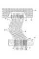
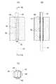
図1を参照するに、プローブカード20は、配線基板22と、配線基板22の下側に配置されたプローブ基板24と、プローブ基板24から下方へ延びる状態にプローブ基板24に配置された棒状の多数のプローブ26とを含む。 Referring to FIG. 1, a probe card 20 includes a
配線基板22は、ガラス入りエポキシ樹脂、セラミック等、電気絶縁性を有する材料で円板状に形成されている。配線基板22は、下面に設けられた導電性の多数の接合部28と、一端部において接合部28に電気的に接続された多数の内部配線30と、上面に設けられた多数の接続部32とを備える。 The
複数の接合部28は、それぞれが複数の接合部28を含む複数の接合部列の形に形成されており、またランドの形を有する。接続部32は、図示の例では、テスタの電気回路に接続されるテスラ-ランドであるが、コネクタの端子であってもよい。 The plurality of
各内部配線30は、接合部28と接続部32とに電気的に接続されている。しかし、コンデンサ、ICリレー、テスト用の集積回路等の複数の電子部品が配線基板22の上面に設けられる場合は、いくつかの内部配線30は接合部28と接続部32とに接続され、残りのいくつかの内部配線30は接合部28と電子部品とに接続され、残りの内部配線30は接続部32と電子部品とに接続される。 Each
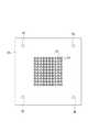
プローブ基板24は、セラミックのような電気絶縁材料により矩形の平面形状に製作されており、また図2(A)及び(B)に詳細に示すように上面及び下面に開口する多数の貫通穴34を中央領域に有すると共に、貫通穴36を4つの隅角部のそれぞれに有する。多数の貫通穴34は、それぞれが複数の貫通穴34を含む複数の貫通穴列の形に形成されており、またプローブ26の上端部を受け入れている。各貫通穴34は、円形の横断面形状を有する。 The
プローブ基板24を配線基板22に対して位置決める位置決めピン(図示せず)は、矩形の1つの対角線の方向に位置する一対の貫通穴36のそれぞれに通すことができる。プローブ基板24を配線基板22に取り付けるボルト(図示せず)は、矩形の他の対角線の方向に位置する一対の貫通穴36のそれぞれに通すことができる。しかし、全ての貫通穴36に位置決めピンを通してもよいし、ボルトが挿入される貫通穴を他の箇所に設けてもよい。 Positioning pins (not shown) for positioning the
各プローブ26は、図示の例では、角柱のように矩形の断面形状を有する。各プローブ26は、上下方向へ延びる針主体部38と、針主体部38の下端から下方へ延びる針先部40と、針主体部38の上端から上方へ延びる取り付け部42とを備える。各プローブ26は、また、下端を被検査体の電極に押圧される針先44とされている。 In the illustrated example, each
各プローブ26は、針主体部38及び針先部40がプローブ基板24から上下方向へ延びる状態に、及び取り付け部42その上端部がプローブ基板24から上方に僅かに突出した状態に、取り付け部42をプローブ基板24の貫通穴34に通されて、その貫通穴34を形成する壁部に導電性接合材(図示せず)により固定されていると共に、上端部において配線基板22の接合部28に導電性接合材(図示せず)により固定されている。 Each
各プローブ26の針主体部38は、同じ方向に湾曲されている。各プローブ26は、フォトレジストに対する露光及びエッチングを行うフォトリソグラフィー技術と、フォトリソグラフィー技術により形成された凹所にニッケル・ボロン、ニッケル・リン等のニッケル合金やニッケル等の金属材料を堆積させるエレクトロフォーミングやスパッタリングのような堆積技術により製作されている。 The needle
プローブ26の形状及び構造、配線基板22及びプローブ基板24とプローブ26との関係は、後に詳細に説明する。 The shape and structure of the
図3を参照して、上記のようなプローブカードの製造方法を以下に説明する。 With reference to FIG. 3, the manufacturing method of the above probe card is demonstrated below.
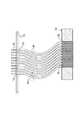
先ず、図2に示すプローブ基板24と、図4に示すタブ付の複数のプローブ板50とが製作される(ステップ200及び201)。プローブ基板24は、セラミックの板材に、貫通穴34,36をレーザ加工、ドリル加工をすることにより得ることができる。 First, the
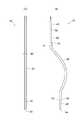
図4に示すように、各プローブ板50は、複数のプローブ52を板状のタブ54に針先部40において分離可能に、一体的に及び並列的に結合している。各プローブ52は、図10から12に示すように、既に述べた、湾曲された変形部を有する針主体部38、針主体部38の下端に続きかつ下端を針先44とされた針先部40、針主体部38の上端に続く取り付け部42に加え、取り付け部42の上端に続きかつ取り付け部42から上方へ延びる先導部46を有する。 As shown in FIG. 4, each
針主体部38、針先部40、取り付け部42及び先導部46は、ニッケル・ボロン合金やニッケル・リンのようなニッケル系の合金、ニッケル等、高い靭性を有する金属材料で一体的に製作されている。少なくとも針先44には、針主体部38のような他の部位の素材より高い硬度を有する金属材料からなる高硬度金属膜が形成されている。そのような高硬度金属膜は、メッキにより形成することができる。 The needle
図10から15に詳細に示すように、針主体部38は、矩形の断面形状を有している。図示の例では、針主体部38の一部を弧状に湾曲させて、その湾曲部を変形部としているが、針主体部38の一部を横V字状に屈曲させて、その屈曲部を変形部としてもよい。針主体部38は、矩形の断面形状を有する。そのような矩形は、図10に示すように、針主体部38の左右方向における寸法(厚さ寸法又は幅寸法)W1が前後方向における寸法W2と同じ又は寸法W2よりやや大きくなる形状とすることができる。 As shown in detail in FIGS. 10 to 15, the needle
針先部40は、寸法W1に対応する寸法が寸法W2対応する寸法より小さい矩形の断面形状を有する上部領域と、寸法W1に対応する寸法が針先44の側の部位ほど小さい下部領域とを有する。このため、針主体部38と針先部40との境界の下向き段部56が左右方向における一方の側及び他方の側のそれぞれに形成されている。 The
取り付け部42は、寸法W1に対応する寸法が寸法W2対応する寸法より小さい矩形の断面形状を有する。取り付け部42は、針主体部38の上端部に対し左右方向における一方の側に変位されている、針主体部38と取り付け部42との境界の上向き段部58が左右方向における一方の側に形成されている。 The
先導部46は、取り付け部42と同軸的に上方へ延びており、また取り付け部42と同じ大きさ及び同じ形状の矩形の断面形状を有する下部領域と、寸法W1に対応する寸法が上端側の部位ほど小さい下部領域とを有する。 The leading
各プローブ26は、また、矩形の対向する2つの辺を形成する2つの面領域の一方の側から他方の側に達する凹所すなわち開口60を上端面に有すると共に、金属層62を、取り付け部42の上端部領域の外周面、該上端部領域に続く領域の相対する2つの面領域、及び開口60を形成する面領域のそれぞれに有し、さらに取り付け部42の上端部領域の3つの外周面の露出部分と、該上端部領域に続く領域の相対する2つの面領域の金属層62とを覆うように設けられた接合材層64を取り付け部42に有する。 Each
図14及び15に示す例では、取り付け部42の上端部領域の外周面に設けられた金属層62は前記上端部領域の周方向全体に設けられており、前記2つの面領域に設けられた金属層62は、前記面領域より小さい幅寸法を有しかつ取り付け部42の長手方向全体にわたって延びる帯の形状を有している。 In the example shown in FIGS. 14 and 15, the
金属層62は、金属層62に対する接合材層64の湿潤性(濡れ性)が取り付け部42に対する接合材層64の湿潤性より高い材料で形成されている。また、接合材層64は、取り付け部42及び金属層62より低い融点を有する金属材料で形成されている。取り付け部42が、ニッケル、ニッケル合金等、ニッケル系の金属材料性である場合、金属層62の素材は、金、金合金、銀、銀合金等、金系又は銀系の金属材料とすることができ、接合材層64の素材は、錫、錫鉛合金等、錫系の金属材料とすることができる。 The
図4に示すように、タブ54は、前後方向におけるプローブ26の厚さ寸法と同じ厚さ寸法を有する矩形の板の形状を有しており、またプローブ26の針主体部38、針先部40及び先導部46と同じ金属材料で一体的に製作されている。タブ54は、図4に示すように、厚さ方向に貫通する多数の穴66を有すると共に、矩形の1つの辺の方向に間隔をおいた多数の凹所68を該矩形の1つの辺に有する。各凹所68には、プローブ26の針先部40が位置されている。 As shown in FIG. 4, the
図12に示すように、各凹所68はΩ字状の形状を有しており、各凹所68の入り口は対向する2つの突出部すなわち結合部70により狭くされている。各結合部70は、三角形の形状を有しており、また三角形の頂点に対応する先端を対向させている。針先部40は、結合部70の先端に一体的に結合されている。 As shown in FIG. 12, each
上記のようなプローブ板50は、前記したフォトリソグラフィー技術と堆積技術とにより製作することができる。 The
図3に戻り、次に上記のようなプローブ板50のプローブ52の取り付け部42が、プローブ基板24の貫通穴34に先導部46の側から挿入される(ステップ202)。取り付け部42の長さ寸法は、プローブ基板24の厚さ寸法より僅かに大きい。このため、図5,16及び17に示すように、取り付け部42は、段部58がプローブ基板24に当接するまで、挿入されると、先導部46の側の端部をプローブ基板から僅かに突出させている。 Returning to FIG. 3, the
段部58がプローブ基板24に当接されていると、貫通穴34へのプローブ52の挿入長さが同じになると共に、プローブ基板24からの取り付け部42の突出長さが同じになるように、各プローブ52の取り付け部42を貫通穴34に容易に挿入することができる。 When the stepped
プローブ52を図5に示すように上下を逆にした状態で、取り付け部42を貫通穴34に挿入すれば、貫通穴34への取り付け部42の挿入作業が容易になる。また、先導部46の下部領域の寸法W1に対応する寸法が上端側の部位ほど小さいことによっても、貫通穴34への取り付け部42の挿入作業が容易になる。 If the
次いで、プローブ基板24とプローブ板50とが加熱されて、接合材層64の材料(接合材)が溶融され、その溶融物が固化される(ステップ203)。その結果、各プローブ52がプローブ基板24の貫通穴34に固定される。 Next, the
既に述べたように、金属層62は、接合材層64の液化物の湿潤性が取り付け部42に対するよりも高い材料で形成されている。したがって、図15に示すように金属層62を覆う接合材層64は、ステップ203において溶融されると、図17に示すように、溶融物すなわち液化物は、自体の表面張力とあいまって、金層62に集中し、その状態で固化することにより、取り付け部42の外周面と貫通穴34を形成している内面とを接合する結合材82となる。その結果、各プローブ52は取り付け部42においてプローブ基板24に固定される。 As already described, the
次いで、図6に示すように、先導部46がタブ付プローブ52から切除され、
各プローブ52がタブ54から針先部40及び結合部70において切り離される(ステップ204)。これにより、各プローブ52はプローブカード20用のプローブ26に変換され、またプローブ組立体が得られる。Next, as shown in FIG. 6, the leading
Each
先導部46の切除作業は、プローブ52の寸法が数十から百数十ミクロンと小さいから、先導部46を取り付け部42から折ることにより、容易に行うことができる。得られたプローブ組立体を図7に示し、図7の底面図20に示す。先導部46の切除により、取り付け部42と先導部46との境界に存在していた開口60は、針主体部38と反対の側に開放しかつV字状の断面形状を有する溝すなわち凹所として作用する。 The cutting operation of the leading
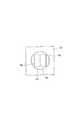
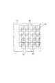
次いで、上記とは別の工程により製造された板状の3つの位置決め部材72が用意される(ステップ205)。各位置決め部材72は、図18に示すように、同じ大きさの矩形の形状を有しており、また厚さ方向に貫通する矩形の多数の貫通穴74を中央領域に複数列に有すると共に、貫通穴76を4つの隅角部のそれぞれに有する。 Next, three plate-
各位置決め部材72は、貫通穴76が変形しない金属材料又は樹脂材料で製作されている。位置決め部材72は、フォトリソグラフィー技術と体積技術とにより製作することができる。 Each positioning
3つの位置決め部材72の貫通穴74は、同じ大きさを有しており、また3つの位置決め部材72が重ねられて、針先部40の厚さ寸法の相当する寸法だけずれた状態に重ね合わされたとき整合する箇所に設けられている。これに対し、3つの位置決め部材72の貫通穴76も、同じ大きさを有しており、また3つの位置決め部材72が正確に重ね合わされた状態において整合する箇所に設けられている。 The through holes 74 of the three
次いで、図8に示すように、貫通穴74が整合する状態に3つの位置決め部材72が重ねられ、その状態において各プローブ26の針先部40が貫通穴74に挿入されて、その後針先部40の相対的位置が仮に固定される(ステップ206)。貫通穴74への針先部40の挿入は、図8に示すように、全ての位置決め部材72の貫通穴74を整列させた状態で、行われる。 Next, as shown in FIG. 8, the three
ステップ206においては、各プローブを、その段部が位置決め部材に当接するまで、針先部を貫通穴に挿入し、その状態で位置決め部材を相対的に変位させることができるから、針先部の相対的位置決めが容易になり、正確になる。 In step 206, each probe is inserted into the through-hole until the stepped portion abuts against the positioning member, and the positioning member can be relatively displaced in this state. Relative positioning is facilitated and accurate.
針先部40の二次元位置の仮固定は、図19に示すように隣り合う位置決め部材72を矩形の対角線の方向に逆に相対的に変位させ、その状態で図9に示すように留め具78を全ての位置決め部材72の貫通穴76に挿し通して仮止めすることにより、行われる。これにより、針先44の相対的な二次元的位置が安定する。 The temporary fixing of the two-dimensional position of the
次いで、針先44の二次元的位置が検査及び調整されて、針先部40の相対的位置が3つの位置決め部材72により維持される(ステップ207)。3つの位置決め部材72を用いる代わりに、2つ又は4つ以上の位置決め部材72を用いてもよい。 Next, the two-dimensional position of the
次いで、全てのプローブ26の接合材82の熱処理が行われる(ステップ208)。この熱処理は、接合材82の溶融温度のほぼ2分の1程度の温度(例えば、錫の場合150°Cから170°C)で数時間(例えば、2時間から3時間)加熱した後、徐冷することにより行われる。 Next, heat treatment is performed on the
上記の熱処理により、各プローブ26の接合材82が変形可能に軟化されるから、各プローブ26の取り付け部42は軟化した接合材82を変形させて貫通穴34に対して変位可能になる。その結果、位置決め部材72により針先44の相対的位置を維持されている起因して、各プローブ26に存在する歪みのような残留応力が除去され、各プローブ26がプローブ基板24に安定に保持されて、プローブ26の針先44の相対的位置関係が安定する。 Since the
ステップ209において、取り付け部42を貫通穴34に固定している接合材82の少なくとも一部も軟化するが、金に対する接合材の濡れ性及び接合材の表面張力により、溶融又は軟化した接合材82は、固化後においては、取り付け部42の外周面と貫通穴34を形成している内面とを接合した状態に戻る。 In
次いで、上記とは別の工程により製造されかつ既に述べた配線基板22が用意される(ステップ210)。 Next, the
次いで、各プローブ26がその取り付け部42の側の端部において配線基板22の接合部28に固定される(ステップ211)。この作業は、各プローブ26の取り付け部42の側の端面が配線基板22の接合部28に当接する状態に、プローブ基板24を配線基板22の1つの面の側に配置し、その状態で少なくとも取り付け部42の端部に存在する接合材82を溶融・固化させることにより行われる。 Next, each
ステップ211において、取り付け部42を貫通穴34に固定している接合材82の少なくとも一部も溶融又は軟化するが、金に対する接合材の濡れ性及び接合材の表面張力により、溶融又は軟化した接合材82は、固化後においては、取り付け部42の外周面と貫通穴42を形成している内面とを接合した状態に戻る。 In
その後、位置決め部材72がプローブ26から取り外される。この作業は、留め具78を除去した後、各位置決め部材72を位置決め部材72から抜き去ることにより、行うことができる。しかし、位置決め部材72を取り去ることなく、すなわち位置決め部材72で針先44の二次元位置を規定した状態で、プローブカードを使用してもよい。この場合、位置決め部材72は電気絶縁材料製とされる。 Thereafter, the positioning
上記の結果、図1に示すプローブカード20が完成される。完成されたプローブカード20においては、取り付け部42と接合部28とを結合している結合材(図示せず)が開口すなわち凹所60(図14参照)に存在するから、取り付け部42への接合材の接触面積が大きく、かつ取り付け部42と接合部28との接合強度が大きい。 As a result, the probe card 20 shown in FIG. 1 is completed. In the completed probe card 20, a bonding material (not shown) that joins the
上記のステップは、適宜変更することができる。 The above steps can be changed as appropriate.
例えば、ステップ203における作業のうち、接合材層64の材料を溶融・固化させて、取り付け部42を貫通穴34に固定する作業は、ステップ211までに行ってもよいし、ステップ211のときに行ってもよい。また、ステップ204における作業のうち、先導部46を取り付け部42から切り離す作業は、ステップ203の前に行ってもよい。 For example, among the operations in
板状のタブ54に結合された複数のプローブ52を用いる代わりに、図21に示すように、それぞれが独立された多数のプローブ52を用いてもよい。 Instead of using the plurality of
本発明は、上記実施例に限定されず、特許請求の範囲に記載された趣旨を逸脱しない限り、種々に変更することができる。 The present invention is not limited to the above-described embodiments, and various modifications can be made without departing from the spirit described in the claims.
20 プローブカード
22 配線基板
24 プローブ基板
26 プローブ
28 接合部
30 内部配線
32 接続部
34,36 貫通穴
38 針主体部
40 針先部
42 取り付け部
44 針先
46 先導部
50 プローブ板
52 プローブ
54 タブ
56,58 段部
60 開口(凹所)
62 金属層
64 接合材層
66 穴
68 凹所
70 結合部
72 位置決め部材
74,76 貫通穴
78 留め具
82 接合材DESCRIPTION OF SYMBOLS 20
62
Claims (10)
Translated fromJapanese各プローブの前記取り付け部をプローブ基板に少なくとも一列に設けられた第1の貫通穴の1つに通す第2の工程と、
厚さ方向に合わされた板状の少なくとも2つの位置決め部材のそれぞれに少なくとも1列に設けられた第2の貫通穴に各プローブの前記針先部を通し、その後隣り合う位置決め部材を逆の方向に相対的に変位させて、前記プローブの針先部の二次元的な位置決めをする第3の工程と、
前記導電性接合材を軟化させて、前記第1の貫通穴に対し各プローブの前記取り付け部を位置決める第4の工程とを含む、プローブカードの製造方法。1st process which manufactures several rod-shaped probes, Comprising: Each probe has the needle main-body part extended to an up-down direction, the needle tip part extended below from the lower end of this needle main-body part, and the upper end of said needle main-body part A first step having an attachment portion extending upward from the upper surface of the attachment portion and a conductive bonding material layer provided on the outer surface of the upper end portion of the attachment portion;
A second step of passing the attachment portion of each probe through one of the first through holes provided in at least one row on the probe substrate;
The probe tip of each probe is passed through a second through-hole provided in at least one row in each of at least two plate-like positioning members aligned in the thickness direction, and then the adjacent positioning members are reversed in the opposite direction. A third step of relatively displacing and two-dimensional positioning of the probe tip of the probe;
And a fourth step of softening the conductive bonding material and positioning the mounting portion of each probe with respect to the first through hole.
前記第3の工程は、前記隣り合う位置決め部材を前記第2の貫通穴の前記矩形の対角線の方向が揃うように合わせることを含み、
前記第3の工程は、前記隣り合う位置決め部材を前記矩形の前記対角線の方向へ相対的に変位させて、その状態に維持することを含む、請求項1及び2のいずれか1項に記載の製造方法。The part that is passed through the second through hole of each probe and each second through hole of each positioning member have a rectangular cross-sectional shape,
The third step includes adjusting the adjacent positioning members so that the diagonal directions of the rectangles of the second through holes are aligned,
3. The method according to claim 1, wherein the third step includes relatively displacing the adjacent positioning members in the diagonal direction of the rectangle and maintaining the state in that state. 4. Production method.
前記第3の工程は、前記針先部を前記第2の貫通穴に通す前に、各プローブと前記タブとを分離することを含む、請求項1から4のいずれか1項に記載の製造方法。The first step includes manufacturing a probe plate in which the plurality of probes are integrally and parallelly coupled to a plate-like tab in a detachable manner at the needle tip portion;
5. The manufacturing according to claim 1, wherein the third step includes separating each probe and the tab before passing the needle tip portion through the second through hole. 6. Method.
前記第2の工程は、各プローブの前記針先部を前記第1の貫通穴に前記先導部の側から通し、
製造方法は、さらに、前記第2の工程の後の任意な時期に、前記プローブの前記先導部を取り付け部から除去する工程と、前記第4の工程の後の任意な時期に、前記位置決め部材を前記プローブから除去する工程とを含む、請求項1から5のいずれか1項に記載の製造方法。Each probe includes a leading portion extending rearward from the rear end portion of the attachment portion,
In the second step, the needle tip portion of each probe is passed through the first through hole from the side of the leading portion,
The manufacturing method further includes the step of removing the leading portion of the probe from the mounting portion at an arbitrary time after the second step, and the positioning member at an arbitrary time after the fourth step. The manufacturing method of any one of Claim 1 to 5 including the process of removing from a said probe.
前記第1の工程は、前記複数のプローブを板状のタブに前記針先部において分離可能に一体的に及び並列的に結合させた複数のプロ−ブ板を製作することを含み、
前記第3の工程は、前記針先部を前記第2の貫通穴に通す前に、各プローブと前記タブとを分離することを含む、請求項1から6のいずれか1項に記載の製造方法。Each of the probe board and each positioning member has the plurality of through holes in a plurality of rows,
The first step includes fabricating a plurality of probe plates in which the plurality of probes are coupled to a plate-shaped tab in a detachable manner at the needle tip portion in an integrated and parallel manner;
The manufacturing according to any one of claims 1 to 6, wherein the third step includes separating each probe and the tab before passing the needle tip portion through the second through hole. Method.
Priority Applications (2)
| Application Number | Priority Date | Filing Date | Title |
|---|---|---|---|
| JP2010183660AJP2012042330A (en) | 2010-08-19 | 2010-08-19 | Manufacturing method of probe card |
| US13/182,254US9015935B2 (en) | 2010-08-19 | 2011-07-13 | Method for manufacturing probe card |
Applications Claiming Priority (1)
| Application Number | Priority Date | Filing Date | Title |
|---|---|---|---|
| JP2010183660AJP2012042330A (en) | 2010-08-19 | 2010-08-19 | Manufacturing method of probe card |
Publications (1)
| Publication Number | Publication Date |
|---|---|
| JP2012042330Atrue JP2012042330A (en) | 2012-03-01 |
Family
ID=45592907
Family Applications (1)
| Application Number | Title | Priority Date | Filing Date |
|---|---|---|---|
| JP2010183660APendingJP2012042330A (en) | 2010-08-19 | 2010-08-19 | Manufacturing method of probe card |
Country Status (2)
| Country | Link |
|---|---|
| US (1) | US9015935B2 (en) |
| JP (1) | JP2012042330A (en) |
Cited By (5)
| Publication number | Priority date | Publication date | Assignee | Title |
|---|---|---|---|---|
| CN105353260A (en)* | 2015-12-25 | 2016-02-24 | 东莞市海轮电子科技有限公司 | A testing device and testing method for connecting terminals |
| EP3026439A2 (en) | 2014-11-26 | 2016-06-01 | Kabushiki Kaisha Nihon Micronics | Contact inspection device |
| JP2018036136A (en)* | 2016-08-31 | 2018-03-08 | 日本電子材料株式会社 | Probe card manufacturing method |
| JP2023520244A (en)* | 2020-04-03 | 2023-05-16 | ファイコム カンパニー リミテッド | Probe card manufacturing jig, probe alignment system including the same, and probe card manufactured using the same |
| WO2025115082A1 (en)* | 2023-11-28 | 2025-06-05 | 日本電子材料株式会社 | Probe and probe card |
Families Citing this family (9)
| Publication number | Priority date | Publication date | Assignee | Title |
|---|---|---|---|---|
| EP3026440B1 (en)* | 2014-11-26 | 2024-08-21 | Kabushiki Kaisha Nihon Micronics | Probe and contact inspection device |
| IT201600127507A1 (en)* | 2016-12-16 | 2018-06-16 | Technoprobe Spa | Contact probe and relative measuring head for an electronic device test device |
| JP6221031B1 (en) | 2016-12-16 | 2017-11-01 | 日本電産リード株式会社 | Contact probe and electrical connection jig |
| JP7005939B2 (en)* | 2017-05-25 | 2022-01-24 | 日本電産リード株式会社 | Contact probe |
| CN110034057A (en)* | 2019-04-26 | 2019-07-19 | 德淮半导体有限公司 | Device, chuck assembly and method for positioning probe |
| JP2021056158A (en)* | 2019-10-01 | 2021-04-08 | 株式会社日本マイクロニクス | Electric contactor, electric connection structure, and electric connection device |
| KR102235344B1 (en) | 2020-12-31 | 2021-04-05 | 황동원 | Contact pin, and a spring contact and test socket with the same for high speed signal ic test |
| JP7658768B2 (en)* | 2021-03-19 | 2025-04-08 | 株式会社日本マイクロニクス | Electrical Connection Device |
| CN114487517B (en)* | 2021-11-11 | 2024-06-07 | 渭南木王智能科技股份有限公司 | Method for processing probe needle formed by crimping multiple tiny needles |
Family Cites Families (12)
| Publication number | Priority date | Publication date | Assignee | Title |
|---|---|---|---|---|
| US3952410A (en)* | 1974-03-28 | 1976-04-27 | Xynetics, Inc. | Probe card including a multiplicity of probe contacts and method of making |
| US4623839A (en)* | 1982-09-17 | 1986-11-18 | Angliatech Limited | Probe device for testing an integrated circuit |
| US5066907A (en)* | 1990-02-06 | 1991-11-19 | Cerprobe Corporation | Probe system for device and circuit testing |
| CA2079418A1 (en)* | 1992-11-18 | 1994-05-19 | Cody Zane Slater | Apparatus and method for manufacturing printed circuit boards |
| US20020053734A1 (en)* | 1993-11-16 | 2002-05-09 | Formfactor, Inc. | Probe card assembly and kit, and methods of making same |
| US20100065963A1 (en)* | 1995-05-26 | 2010-03-18 | Formfactor, Inc. | Method of wirebonding that utilizes a gas flow within a capillary from which a wire is played out |
| US7262611B2 (en)* | 2000-03-17 | 2007-08-28 | Formfactor, Inc. | Apparatuses and methods for planarizing a semiconductor contactor |
| US7143500B2 (en)* | 2001-06-25 | 2006-12-05 | Micron Technology, Inc. | Method to prevent damage to probe card |
| US6729019B2 (en)* | 2001-07-11 | 2004-05-04 | Formfactor, Inc. | Method of manufacturing a probe card |
| JP4217468B2 (en)* | 2002-12-03 | 2009-02-04 | 株式会社アドバンテスト | Method of connecting probe pins to wiring board and method of manufacturing probe card |
| JP2009162483A (en) | 2007-12-28 | 2009-07-23 | Micronics Japan Co Ltd | Electrical connection device |
| US8310259B2 (en)* | 2008-02-01 | 2012-11-13 | International Business Machines Corporation | Silicon carrier space transformer and temporary chip attach burn-in vehicle for high density connections |
- 2010
- 2010-08-19JPJP2010183660Apatent/JP2012042330A/enactivePending
- 2011
- 2011-07-13USUS13/182,254patent/US9015935B2/enactiveActive
Cited By (8)
| Publication number | Priority date | Publication date | Assignee | Title |
|---|---|---|---|---|
| EP3026439A2 (en) | 2014-11-26 | 2016-06-01 | Kabushiki Kaisha Nihon Micronics | Contact inspection device |
| KR20160063286A (en) | 2014-11-26 | 2016-06-03 | 가부시키가이샤 니혼 마이크로닉스 | Contact inspection device |
| US10215801B2 (en) | 2014-11-26 | 2019-02-26 | Kabushiki Kaisha Nihon Micronics | Contact inspection device having a probe head and rotation restricting portions |
| CN105353260A (en)* | 2015-12-25 | 2016-02-24 | 东莞市海轮电子科技有限公司 | A testing device and testing method for connecting terminals |
| CN105353260B (en)* | 2015-12-25 | 2019-01-08 | 东莞市海轮电子科技有限公司 | Testing device and testing method for connecting terminal |
| JP2018036136A (en)* | 2016-08-31 | 2018-03-08 | 日本電子材料株式会社 | Probe card manufacturing method |
| JP2023520244A (en)* | 2020-04-03 | 2023-05-16 | ファイコム カンパニー リミテッド | Probe card manufacturing jig, probe alignment system including the same, and probe card manufactured using the same |
| WO2025115082A1 (en)* | 2023-11-28 | 2025-06-05 | 日本電子材料株式会社 | Probe and probe card |
Also Published As
| Publication number | Publication date |
|---|---|
| US9015935B2 (en) | 2015-04-28 |
| US20120042509A1 (en) | 2012-02-23 |
Similar Documents
| Publication | Publication Date | Title |
|---|---|---|
| JP5487050B2 (en) | Probe card manufacturing method | |
| JP2012042330A (en) | Manufacturing method of probe card | |
| TWI517326B (en) | Substrate having leads | |
| US9000793B2 (en) | Fine pitch probes for semiconductor testing, and a method to fabricate and assemble same | |
| US7548082B2 (en) | Inspection probe | |
| KR101034979B1 (en) | Contact for electrical test of electronic device, probe assembly and manufacturing method thereof | |
| TW200841020A (en) | Lateral interposer contact design and probe card assembly | |
| JP2009508141A (en) | Lateral interposer contact design and probe card assembly | |
| JP2002116224A (en) | Combination members for multiplex chip probe and general-purpose tester contact point and manufacturing method thereof | |
| JP2008530580A (en) | Probe card assembly and method of attaching a probe to the probe card assembly | |
| TW200840150A (en) | Probe card including a plurality of connectors and method of bonding the connectors to a substrate of the probe card | |
| JP2009270880A5 (en) | ||
| TW200809215A (en) | Contactor assembly | |
| JP5487049B2 (en) | Probe card | |
| JP7471778B2 (en) | Probe Card | |
| US7316065B2 (en) | Method for fabricating a plurality of elastic probes in a row | |
| JP2004003911A (en) | Laminated probe, jig for producing laminated probe, method for producing laminated probe, and vertical probe card using laminated probe | |
| KR101757742B1 (en) | Probe and Probe Manufacturing Method | |
| JP5342418B2 (en) | Electrical test probe and electrical connection device using the same | |
| US9329206B2 (en) | Probe card and method for manufacturing the same | |
| JP3962264B2 (en) | Contact probe and manufacturing method thereof | |
| US20240347237A1 (en) | Built-in chip resistor for substrate, resistor built-in module, manufacturing method of resistor built-in module, and trimming | |
| JP2009092484A (en) | How to make a probe | |
| JP4812967B2 (en) | Probe card and probe card manufacturing method | |
| JP3996124B2 (en) | Probe card manufacturing method |