JP2012028859A - Variable gain differential amplifier circuit - Google Patents
Variable gain differential amplifier circuitDownload PDFInfo
- Publication number
- JP2012028859A JP2012028859AJP2010163005AJP2010163005AJP2012028859AJP 2012028859 AJP2012028859 AJP 2012028859AJP 2010163005 AJP2010163005 AJP 2010163005AJP 2010163005 AJP2010163005 AJP 2010163005AJP 2012028859 AJP2012028859 AJP 2012028859A
- Authority
- JP
- Japan
- Prior art keywords
- transistors
- current
- transistor
- pair
- circuit
- Prior art date
- Legal status (The legal status is an assumption and is not a legal conclusion. Google has not performed a legal analysis and makes no representation as to the accuracy of the status listed.)
- Pending
Links
- 230000003321amplificationEffects0.000claimsabstractdescription14
- 238000003199nucleic acid amplification methodMethods0.000claimsabstractdescription14
- 230000000295complement effectEffects0.000claimsdescription11
- 238000010586diagramMethods0.000description15
- 230000003068static effectEffects0.000description13
- 230000003287optical effectEffects0.000description8
- 238000012546transferMethods0.000description7
- 238000001514detection methodMethods0.000description4
- 238000004891communicationMethods0.000description3
- 150000001875compoundsChemical class0.000description3
- 239000004065semiconductorSubstances0.000description3
- 230000002457bidirectional effectEffects0.000description2
- 230000000694effectsEffects0.000description2
- 230000003334potential effectEffects0.000description2
- 230000000087stabilizing effectEffects0.000description2
- 238000013459approachMethods0.000description1
- 238000007796conventional methodMethods0.000description1
- 230000007423decreaseEffects0.000description1
- 230000005669field effectEffects0.000description1
- 125000005842heteroatomChemical group0.000description1
Images


Classifications
- H—ELECTRICITY
- H03—ELECTRONIC CIRCUITRY
- H03F—AMPLIFIERS
- H03F3/00—Amplifiers with only discharge tubes or only semiconductor devices as amplifying elements
- H03F3/45—Differential amplifiers
- H03F3/45071—Differential amplifiers with semiconductor devices only
- H03F3/45076—Differential amplifiers with semiconductor devices only characterised by the way of implementation of the active amplifying circuit in the differential amplifier
- H03F3/4508—Differential amplifiers with semiconductor devices only characterised by the way of implementation of the active amplifying circuit in the differential amplifier using bipolar transistors as the active amplifying circuit
- H03F3/45098—PI types
- H—ELECTRICITY
- H03—ELECTRONIC CIRCUITRY
- H03F—AMPLIFIERS
- H03F3/00—Amplifiers with only discharge tubes or only semiconductor devices as amplifying elements
- H03F3/04—Amplifiers with only discharge tubes or only semiconductor devices as amplifying elements with semiconductor devices only
- H03F3/08—Amplifiers with only discharge tubes or only semiconductor devices as amplifying elements with semiconductor devices only controlled by light
- H03F3/087—Amplifiers with only discharge tubes or only semiconductor devices as amplifying elements with semiconductor devices only controlled by light with IC amplifier blocks
- H—ELECTRICITY
- H03—ELECTRONIC CIRCUITRY
- H03F—AMPLIFIERS
- H03F3/00—Amplifiers with only discharge tubes or only semiconductor devices as amplifying elements
- H03F3/45—Differential amplifiers
- H03F3/45071—Differential amplifiers with semiconductor devices only
- H03F3/45076—Differential amplifiers with semiconductor devices only characterised by the way of implementation of the active amplifying circuit in the differential amplifier
- H03F3/4508—Differential amplifiers with semiconductor devices only characterised by the way of implementation of the active amplifying circuit in the differential amplifier using bipolar transistors as the active amplifying circuit
- H03F3/45098—PI types
- H03F3/45103—Non-folded cascode stages
- H—ELECTRICITY
- H03—ELECTRONIC CIRCUITRY
- H03F—AMPLIFIERS
- H03F3/00—Amplifiers with only discharge tubes or only semiconductor devices as amplifying elements
- H03F3/45—Differential amplifiers
- H03F3/45071—Differential amplifiers with semiconductor devices only
- H03F3/45076—Differential amplifiers with semiconductor devices only characterised by the way of implementation of the active amplifying circuit in the differential amplifier
- H03F3/45475—Differential amplifiers with semiconductor devices only characterised by the way of implementation of the active amplifying circuit in the differential amplifier using IC blocks as the active amplifying circuit
- H—ELECTRICITY
- H03—ELECTRONIC CIRCUITRY
- H03G—CONTROL OF AMPLIFICATION
- H03G3/00—Gain control in amplifiers or frequency changers
- H03G3/20—Automatic control
- H03G3/30—Automatic control in amplifiers having semiconductor devices
- H03G3/3084—Automatic control in amplifiers having semiconductor devices in receivers or transmitters for electromagnetic waves other than radiowaves, e.g. lightwaves
- H—ELECTRICITY
- H03—ELECTRONIC CIRCUITRY
- H03F—AMPLIFIERS
- H03F2203/00—Indexing scheme relating to amplifiers with only discharge tubes or only semiconductor devices as amplifying elements covered by H03F3/00
- H03F2203/45—Indexing scheme relating to differential amplifiers
- H03F2203/45138—Two or more differential amplifiers in IC-block form are combined, e.g. measuring amplifiers
- H—ELECTRICITY
- H03—ELECTRONIC CIRCUITRY
- H03F—AMPLIFIERS
- H03F2203/00—Indexing scheme relating to amplifiers with only discharge tubes or only semiconductor devices as amplifying elements covered by H03F3/00
- H03F2203/45—Indexing scheme relating to differential amplifiers
- H03F2203/45302—Indexing scheme relating to differential amplifiers the common gate stage of a cascode dif amp being controlled
- H—ELECTRICITY
- H03—ELECTRONIC CIRCUITRY
- H03F—AMPLIFIERS
- H03F2203/00—Indexing scheme relating to amplifiers with only discharge tubes or only semiconductor devices as amplifying elements covered by H03F3/00
- H03F2203/45—Indexing scheme relating to differential amplifiers
- H03F2203/45702—Indexing scheme relating to differential amplifiers the LC comprising two resistors
Landscapes
- Engineering & Computer Science (AREA)
- Power Engineering (AREA)
- Physics & Mathematics (AREA)
- Electromagnetism (AREA)
- Amplifiers (AREA)
- Control Of Amplification And Gain Control (AREA)
Abstract
Translated fromJapaneseDescription
Translated fromJapanese本発明は、利得可変差動増幅回路に関するものである。 The present invention relates to a variable gain differential amplifier circuit.
特許文献1には、図9に示される通信用の利得可変増幅器が開示されている。この利得可変増幅器100は、エミッタ同士が相互に接続された一対のトランジスタ101及び102と、トランジスタ101のコレクタ側に接続され且つエミッタ同士が相互に接続された一対のトランジスタ103及び104と、トランジスタ102のコレクタ側に接続され且つエミッタ同士が相互に接続された一対のトランジスタ105及び106とを備える。トランジスタ103及び106のコレクタは、それぞれ負荷抵抗107及び108を介して電源線109に接続されている。トランジスタ104及び105のコレクタは、電流加算器110及び電流分配器111を介して負荷抵抗107及び108にそれぞれ接続されている。トランジスタ101及び102のエミッタには電流源112が接続されている。 Patent Document 1 discloses a variable gain amplifier for communication shown in FIG. The
特許文献2には、差動対を用いた利得可変増幅器に使用される直流レベル安定化回路が開示されている。図10は、この直流レベル安定化回路を含む利得可変増幅器200の構成を示す回路図である。利得可変増幅器200は、図9に示された利得可変増幅器100と同様の構成を有するトランジスタ101〜106、負荷抵抗107,108及び電流源112を備える。また、この利得可変増幅器200では、トランジスタ104,105を流れる電流に比例する電流が、カレントミラー回路120,121によって負荷抵抗107,108に流れる。これにより、直流電位差を一定とし、ダイナミックレンジのみを拡大する。 Patent Document 2 discloses a DC level stabilizing circuit used for a variable gain amplifier using a differential pair. FIG. 10 is a circuit diagram showing a configuration of
特許文献3には、温度や電源電圧の変動によって出力電位が変化しないように、動作点を補償しつつ自動利得制御を行う利得可変増幅器が開示されている。図11は、この利得可変増幅器300の構成を示す回路図である。利得可変増幅器300は、利得制御部310、整合回路320、及び差動増幅器330からなる。利得制御部310は、トランジスタ101〜106、負荷抵抗107,108及び電流源112を備える。負荷抵抗107,108と電源線109との間には、トランジスタ131が更に接続されている。また、整合回路320は2段のエミッタフォロア回路を有しており、トランジスタ103,106のエミッタ電位を増幅して差動増幅器330へ出力する。差動増幅器330は、エミッタ同士が相互に接続された一対のトランジスタ132及び133を有する。 Patent Document 3 discloses a variable gain amplifier that performs automatic gain control while compensating for the operating point so that the output potential does not change due to fluctuations in temperature or power supply voltage. FIG. 11 is a circuit diagram showing a configuration of the
この利得可変増幅器300では、後段の差動増幅器330における出力電圧の変動をも補償するようにフィードバック回路が構成されている。すなわち、差動増幅器330の一対のトランジスタ132及び133の共通エミッタ電位をトランジスタ135によって検出し、このエミッタ電位の変動を、トランジスタ131を介して一対のトランジスタ101及び102の電源電圧に反映させている。 In this
図12は、バイポーラトランジスタを備える一般的な利得可変差動増幅回路の構成を示す回路図である。この利得可変差動増幅回路400は、エミッタ同士が抵抗410を介して相互に接続された一対の差動トランジスタ401及び402と、差動トランジスタ401のコレクタ側に接続され且つエミッタ同士が相互に接続された一対のトランジスタ403及び404と、差動トランジスタ402のコレクタ側に接続され且つエミッタ同士が相互に接続された一対のトランジスタ405及び406とを備える。トランジスタ403及び406のコレクタは、それぞれ負荷抵抗407及び408を介して電源線409に接続されている。トランジスタ404及び405のコレクタは、電源線409に直接接続されている。差動トランジスタ401のエミッタには電流源412が接続され、差動トランジスタ402のエミッタには電流源413が接続されている。差動トランジスタ401及び402の各ベースには、高周波の相補的な信号Vinが入力される。トランジスタ403及び406のベースと、トランジスタ404及び405のベースとのそれぞれには、相補的な利得制御信号Vcが入力される。そして、トランジスタ403,406のコレクタ電位が出力電圧Vout1,Vout2として取り出される。FIG. 12 is a circuit diagram showing a configuration of a general variable gain differential amplifier circuit including a bipolar transistor. In the variable gain differential amplifier circuit 400, a pair of
この利得可変差動増幅回路400では、トランジスタ403及び406を流れる電流量が、利得制御信号Vcによって制御される。これにより、負荷抵抗407,408を流れる電流量を可変とし、この利得可変差動増幅回路400への入力信号Vinに対する出力電圧Vout1,Vout2の利得を変化させることができる。In the variable gain differential amplifier circuit 400, the amount of current flowing through the
ここで、トランジスタ403及び406を流れる電流の大きさは、次の数式IQによって表される。この数式において、I1は、電流源412,413によって規定される直流成分であり、制御信号Vcによってトランジスタ403及び404、並びにトランジスタ405及び406のそれぞれに振り分けられる。i1は、入力信号Vinによって生じる交流成分であり、トランジスタ401,402に相対的に振り分けられる。VTは電子の熱エネルギーであり、Tは絶対温度である。室温でVTは約25mVの値を有する。
この数式の右辺は、出力電圧Vout1(またはVout2)に含まれる直流成分を決定する電流I1に関する項と、利得および出力振幅を決定する電流i1に関する項とからなり、何れの項の値も利得制御信号Vcによって変化する。すなわち、利得を変化させる為に利得制御信号Vcを変化させると、電流I1に関する項によって、出力電圧Vout1(またはVout2)の出力振幅だけでなく直流成分の大きさも変動する。そして、出力電圧Vout1(またはVout2)のダイナミックレンジを広くすると、この直流成分の変動も更に大きくなってしまう。直流成分の大きな変動は、利得可変差動増幅回路の出力信号波形の歪み、後段に接続される増幅器の定格入力電圧範囲の上限値に近づくことによる歪み、或いは、振幅検出回路から利得制御回路までを含むフィードバックループの不安定性の原因となる。The right side of this equation is composed of a term related to the current I1 that determines the DC component included in the output voltage Vout1 (or Vout2 ) and a term related to the current i1 that determines the gain and output amplitude. The value also changes depending on the gain control signal Vc. That is, when the gain control signal Vc is changed in order to change the gain, not only the output amplitude of the output voltage Vout1 (or Vout2 ) but also the magnitude of the DC component varies depending on the term relating to the current I1 . When the dynamic range of the output voltage Vout1 (or Vout2 ) is widened, the fluctuation of the direct current component is further increased. The large fluctuation of the DC component is caused by distortion of the output signal waveform of the variable gain differential amplifier circuit, distortion caused by approaching the upper limit value of the rated input voltage range of the amplifier connected to the subsequent stage, or from the amplitude detection circuit to the gain control circuit. This causes instability of the feedback loop including.
本発明は、このような問題点に鑑みてなされたものであり、利得を変化させた場合に、出力電圧に含まれる直流成分の変動を抑えることができる利得可変差動増幅回路を提供することを目的とする。 The present invention has been made in view of such a problem, and provides a variable gain differential amplifier circuit capable of suppressing fluctuations in a DC component included in an output voltage when the gain is changed. With the goal.
上述した課題を解決するために、本発明による利得可変差動増幅回路は、増幅段及び調整段を備える利得可変差動増幅回路であって、増幅段は、一方の電流端子が互いに接続された一対のトランジスタ(Q1,Q2)を含み、該一対のトランジスタ(Q1,Q2)の制御端子に相補的な入力信号を受ける第1の差動回路、一方の電流端子が互いに接続された一対のトランジスタ(Q3,Q4)を含む第2の差動回路、一方の電流端子が互いに接続された一対のトランジスタ(Q5,Q6)を含む第3の差動回路、及び一対のトランジスタ(Q1,Q2)の一方の電流端子に接続された第1の電流源を有し、一対のトランジスタ(Q3,Q4)の一方の電流端子が一対のトランジスタ(Q1,Q2)のうち一方の第1のトランジスタ(Q1)の他方の電流端子に接続されており、一対のトランジスタ(Q5,Q6)の一方の電流端子が一対のトランジスタ(Q1,Q2)のうち他方の第1のトランジスタ(Q2)の他方の電流端子に接続されており、正負2つの信号からなる互いに相補的な制御信号のうち一方の制御信号がトランジスタ(Q3,Q6)の制御端子に入力され、他方の制御信号がトランジスタ(Q4,Q5)の制御端子に入力され、トランジスタ(Q3,Q6)の他方の電流端子が負荷抵抗を介して電源線に接続されており、トランジスタ(Q4,Q5)の他方の電流端子が電源線に直接接続されており、調整段は、一方の電流端子が互いに接続された一対のトランジスタ(Q7,Q8)を含む第4の差動回路、一対のトランジスタ(Q7,Q8)の一方の電流端子に接続された第2の電流源、一方の電流端子が互いに接続された一対のトランジスタ(Q9,Q10)を含む第5の差動回路、及び一対のトランジスタ(Q9,Q10)の一方の電流端子に接続された第3の電流源を有し、一方の制御信号がトランジスタ(Q7,Q10)の制御端子に入力され、他方の制御信号がトランジスタ(Q8,Q9)の制御端子に入力され、トランジスタ(Q7,Q10)の他方の電流端子が電源線に直接接続されており、トランジスタ(Q8,Q9)の他方の電流端子が負荷抵抗を介して電源線に接続されていることを特徴とする。 In order to solve the above-described problem, a variable gain differential amplifier circuit according to the present invention is a variable gain differential amplifier circuit including an amplification stage and an adjustment stage, and the amplification stage has one current terminal connected to each other. A first differential circuit including a pair of transistors (Q1, Q2) and receiving a complementary input signal at the control terminals of the pair of transistors (Q1, Q2); a pair of transistors having one current terminal connected to each other A second differential circuit including (Q3, Q4), a third differential circuit including a pair of transistors (Q5, Q6) having one current terminal connected to each other, and a pair of transistors (Q1, Q2). A first current source connected to one current terminal, and one current terminal of the pair of transistors (Q3, Q4) is one first transistor (Q1) of the pair of transistors (Q1, Q2). of One of the pair of transistors (Q5, Q6) is connected to the other current terminal of the other first transistor (Q2) of the pair of transistors (Q1, Q2). One of the complementary control signals consisting of two positive and negative signals is input to the control terminal of the transistor (Q3, Q6), and the other control signal is the control terminal of the transistor (Q4, Q5). And the other current terminal of the transistor (Q3, Q6) is connected to the power supply line via the load resistor, and the other current terminal of the transistor (Q4, Q5) is directly connected to the power supply line, The adjustment stage includes a fourth differential circuit including a pair of transistors (Q7, Q8) having one current terminal connected to each other, and one current terminal of the pair of transistors (Q7, Q8). A second current source that is connected, a fifth differential circuit including a pair of transistors (Q9, Q10) with one current terminal connected to each other, and one current terminal of the pair of transistors (Q9, Q10) A third current source connected, one control signal is input to the control terminal of the transistor (Q7, Q10), the other control signal is input to the control terminal of the transistor (Q8, Q9), The other current terminal of Q7, Q10) is directly connected to the power supply line, and the other current terminal of the transistors (Q8, Q9) is connected to the power supply line via a load resistor.
また、利得可変差動増幅回路は、第2及び第3の電流源によって規定される電流値が、第1の電流源によって規定される電流値の1/2であることを特徴としてもよい。 The variable gain differential amplifier circuit may be characterized in that a current value defined by the second and third current sources is ½ of a current value defined by the first current source.
また、利得可変差動増幅回路は、トランジスタ(Q1ないしQ10)がnpnトランジスタであることを特徴としてもよい。 The variable gain differential amplifier circuit may be characterized in that the transistors (Q1 to Q10) are npn transistors.
また、利得可変差動増幅回路は、トランジスタ(Q1ないしQ10)がヘテロバイポーラトランジスタであることを特徴としてもよい。 The variable gain differential amplifier circuit may be characterized in that the transistors (Q1 to Q10) are heterobipolar transistors.
また、利得可変差動増幅回路は、一対のトランジスタ(Q1,Q2)それぞれの一方の電流端子に二つの第1の電流源それぞれが接続されており、一対のトランジスタ(Q1,Q2)の各一方の電流端子が抵抗を介して互いに接続されていることを特徴としてもよい。 The variable gain differential amplifier circuit has two first current sources connected to one current terminal of each of the pair of transistors (Q1, Q2), and each one of the pair of transistors (Q1, Q2). The current terminals may be connected to each other through a resistor.
本発明による利得可変差動増幅回路によれば、利得を変化させた場合に、出力電圧に含まれる直流成分の変動を抑えることができる。 According to the variable gain differential amplifier circuit of the present invention, it is possible to suppress fluctuations in the DC component included in the output voltage when the gain is changed.
以下、添付図面を参照しながら本発明による利得可変差動増幅回路の実施の形態を詳細に説明する。なお、図面の説明において同一の要素には同一の符号を付し、重複する説明を省略する。また、トランジスタとはバイポーラトランジスタ及び電界効果トランジスタ(FET)の双方を含む。以下の説明ではトランジスタがバイポーラトランジスタである場合を例示するが、トランジスタがFETである場合、ベース、エミッタ及びコレクタはそれぞれゲート、ソース及びドレインと置き換えられる。 Embodiments of a variable gain differential amplifier circuit according to the present invention will be described below in detail with reference to the accompanying drawings. In the description of the drawings, the same elements are denoted by the same reference numerals, and redundant description is omitted. Transistors include both bipolar transistors and field effect transistors (FETs). In the following description, the case where the transistor is a bipolar transistor is illustrated, but when the transistor is an FET, the base, the emitter, and the collector are replaced with the gate, the source, and the drain, respectively.
図1は、本発明の一実施形態に係る利得可変差動増幅回路を備える光受信装置の構成を示すブロック図である。この光受信装置10は、フォトダイオードPDからの光電流Ipdを電圧信号に変換し、増幅して出力するための装置である。図1に示されるように、光受信装置10は、トランスインピーダンスアンプ(TIA)11、2つの利得可変差動増幅回路12及び13、振幅検出回路26、及び利得制御回路27を備える。加えて、光受信装置10は、差動増幅器28及びオフセット補償回路29を備える。 FIG. 1 is a block diagram showing a configuration of an optical receiving apparatus including a variable gain differential amplifier circuit according to an embodiment of the present invention. The
フォトダイオードPDに高周波の信号光が入射すると、フォトダイオードPDは該信号光に対応する光電流Ipdを生成する。光電流Ipdは、光受信装置10の入力端子10aを経てTIA11に入力される。TIA11は、光電流Ipdに応じた電圧信号Vinを生成する。電圧信号Vinは、利得可変差動増幅回路12及び13に順次入力され、増幅される。利得可変差動増幅回路13から出力された電圧信号は、差動増幅器28によって更に増幅され、光受信装置10の出力端子10bを経て外部へ出力される。 When high-frequency signal light is incident on the photodiode PD, the photodiode PD generates a photocurrent Ipd corresponding to the signal light. The photocurrent Ipd is input to the TIA 11 through the
振幅検出回路26は、利得可変差動増幅回路13から出力された電圧信号の振幅を検出する。電圧信号の振幅に関する情報は、利得制御回路27へ提供される。利得制御回路27は、利得可変差動増幅回路12及び13へ利得制御信号Vcを提供する。利得制御信号Vcは、電圧信号の振幅が所定の大きさとなるように、利得可変差動増幅回路12及び13から出力される電圧信号の振幅を調整する為の信号である。また、オフセット補償回路29は、利得可変差動増幅回路12のオフセットを調整するためのフィードバック回路であり、差動増幅器28から出力された電圧信号を入力し、この電圧信号に基づいて利得可変差動増幅回路12のオフセットを調整する。 The
図2は、利得可変差動増幅回路12の回路構成を示す図である。なお、利得可変差動増幅回路13は、この利得可変差動増幅回路12と同様の回路構成を有することができる。図2に示されるように、本実施形態の利得可変差動増幅回路12は、増幅段12A及び調整段12Bを備える。増幅段12Aは、第1の差動回路13、第2の差動回路14、第3の差動回路15、及び第1の電流源16a,16bを有する。 FIG. 2 is a diagram showing a circuit configuration of the variable gain
第1の差動回路13は、一対の差動トランジスタQ1及びQ2を含む。差動トランジスタQ1及びQ2の各エミッタ(一方の電流端子)は、抵抗17を介して互いに接続されている。また、差動トランジスタQ1のエミッタには第1の電流源16aが接続されており、差動トランジスタQ2のエミッタには第1の電流源16bが接続されている。差動トランジスタQ1及びQ2のベース(制御端子)には、図1に示されたTIA11から相補的な高周波の交流信号Vinが入力される。 The first
第2の差動回路14は、一対のトランジスタQ3及びQ4を含む。トランジスタQ3及びQ4の各エミッタ(一方の電流端子)は、互いに接続され、且つ差動トランジスタQ1のコレクタ(他方の電流端子)と接続されている。また、トランジスタQ3のコレクタ(他方の電流端子)は負荷抵抗18を介して電源線20に接続されており、トランジスタQ4のコレクタは電源線20に直接(すなわち有意な抵抗を介することなく)接続されている。 The second
第3の差動回路15は、一対のトランジスタQ5及びQ6を含む。トランジスタQ5及びQ6の各エミッタ(一方の電流端子)は、互いに接続され、且つ差動トランジスタQ2のコレクタと接続されている。また、トランジスタQ5のコレクタ(他方の電流端子)は電源線20に直接接続されており、トランジスタQ6のコレクタは負荷抵抗19を介して電源線20に接続されている。 The third
トランジスタQ3及びQ6のベース(制御端子)には、利得制御信号Vc+が入力される。また、トランジスタQ4及びQ5のベースには、利得制御信号Vc−が入力される。利得制御信号Vc+及びVc−は、正負2つの信号からなる互いに相補的な利得制御信号Vc(図1を参照)を構成する。The gain control signal Vc+ is input to the bases (control terminals) of the transistors Q3 and Q6. Further, the bases of the transistors Q4 and Q5, the gain control signal Vc- is entered. Gain control signal Vc+ and Vc- constitutes consists two positive and negative signals complementary to each other gain control signal Vc (see Figure 1).
調整段12Bは、第4の差動回路21、第5の差動回路22、第2の電流源23、及び第3の電流源24を有する。 The
第4の差動回路21は、一対のトランジスタQ7及びQ8を含む。トランジスタQ7及びQ8の各エミッタ(一方の電流端子)は、互いに接続され、且つ第2の電流源23に接続されている。また、トランジスタQ7のコレクタ(他方の電流端子)は電源線20に直接接続されており、トランジスタQ8のコレクタは負荷抵抗18を介して電源線20に接続されている。 The fourth
第5の差動回路22は、一対のトランジスタQ9及びQ10を含む。トランジスタQ9及びQ10の各エミッタ(一方の電流端子)は、互いに接続され、且つ第3の電流源24に接続されている。また、トランジスタQ9のコレクタ(他方の電流端子)は負荷抵抗19を介して電源線20に接続されており、トランジスタQ10のコレクタは電源線20に直接接続されている。 The fifth
トランジスタQ7及びQ10のベース(制御端子)には、上述した利得制御信号Vc+が入力される。また、トランジスタQ8及びQ9のベースには、上述した利得制御信号Vc−が入力される。The above-described gain control signal Vc+ is input to the bases (control terminals) of the transistors Q7 and Q10. Further, the bases of the transistors Q8 and Q9, the gain control signal Vc as described above- is entered.
トランジスタQ1〜Q10は、npnトランジスタであることが好ましく、また、ヘテロバイポーラトランジスタであることが好ましい。これにより、図2に示された第1ないし第5の差動回路13〜15、21及び22を好適に構成することができる。 Transistors Q1-Q10 are preferably npn transistors and are preferably heterobipolar transistors. Thereby, the 1st thru | or 5th differential circuits 13-15, 21, and 22 shown by FIG. 2 can be comprised suitably.
以上の構成を備える利得可変差動増幅回路12の作用および効果について、従来技術とその課題を踏まえて説明する。 The operation and effect of the variable gain
図3は、差動増幅回路の利得を可変とするための一般的な回路構成を示す図である。図3に示される回路30は、2本の電流経路30a及び30bを有する。電流経路30aは、負荷抵抗31aと、差動対の一方を構成するトランジスタ32aと、電流源33aとが直列に接続されて成る。同様に、電流経路30bは、負荷抵抗31bと、差動対の他方を構成するトランジスタ32bと、電流源33bとが直列に接続されて成る。電流経路30a及び30bの一端は電源線34に接続されている。相補的な入力信号InP及びInNのうち一方の入力信号InPはトランジスタ32aのベースに入力され、他方の入力信号InNはトランジスタ32bのベースに入力される。トランジスタ32a及び32bのコレクタ電位は、この回路30の出力信号として取り出される。 FIG. 3 is a diagram showing a general circuit configuration for making the gain of the differential amplifier circuit variable. The
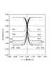
これら2本の電流経路30a及び30bの各トランジスタ32a及び32bのエミッタ間に抵抗35を接続し、且つこの抵抗35の値を可変とすることにより、利得を可変とすることができる。図4は、この回路30の静特性(入力信号InP,InNから出力信号への伝達特性のうち、直流成分のみに関する特性)を示すグラフである。図4の縦軸はトランジスタ32a及び32bのコレクタ出力(すなわち出力信号電圧)を示しており、横軸はトランジスタ32a及び32bのベース電位差(すなわち入力信号InP,InNの電位差)を示している。また、図4に示されるグラフG11〜G15はトランジスタ32aのコレクタ出力を示し、グラフG21〜G25はトランジスタ32bのコレクタ出力を示す。また、これらのグラフG11〜G15のそれぞれは、抵抗35がそれぞれ0Ω、100Ω、200Ω、500Ω、及び1kΩである場合に対応している。同様に、グラフG21〜G25のそれぞれは、抵抗35がそれぞれ0Ω、100Ω、200Ω、500Ω、及び1kΩである場合に対応している。なお、図4では、電源線34の電源電圧値として3.3Vを仮定している。また、以下の説明では、理解の容易のためトランジスタ32aをオフ側トランジスタ、トランジスタ32bをオン側トランジスタとして説明する。 By connecting a
図4に示されるように、一対のトランジスタ32a,32bのうち一方(オフ側)のトランジスタ32aのコレクタ電位は、電源電圧(3.3V)と等しくなる。また、他方(オン側)のトランジスタ32bには、二つの電流源33a及び33bによる電流が全て流れる。すなわち、この電流は一方の負荷抵抗31bを流れることとなり、電位効果が生じてその分だけトランジスタ32bのコレクタ電位が低下する。なお、一実施例では、電流源33a及び33bの電流値は各々0.5mAである。また、負荷抵抗31a,31bの大きさは例えば1kΩである。この場合、上記電位効果は1Vであり、トランジスタ32bのコレクタ電位は2.3Vに低下する。 As shown in FIG. 4, the collector potential of one (off-side)
また、抵抗35が有限の値に設定された場合、オフ側のトランジスタ32aを含む電流経路30aの電流源33aからの電流帰還作用が働くので、オン側のトランジスタ32bのエミッタ電位が上昇する。この作用は、トランジスタ32bのベースバイアスを低下させることに繋がるので、当該電流経路30bの出力電圧の利得が減少する。しかし、最終的に、オン側トランジスタ32bを流れる電流は、二つの電流源33a及び33bの電流の和となる。したがって、該トランジスタ32bのコレクタ出力のオフレベル及びオンレベルに変化はなく、図4に示されるような特性を得ることができる。 When the
しかしながら、図3に示された回路30の抵抗35においては、電流が双方向に流れうることが必要があるが、バイポーラトランジスタ(化合物半導体に限らない)で双方向の等価抵抗特性を得るのは極めて困難である。もし双方向の等価抵抗特性を実現できたとしても、その動作範囲は極めて狭く、バイアス条件がポイント的となり実用的ではない。そこで、FET(特にMOSFET)をアクティブ抵抗として利用することが想定されるが、化合物半導体を主な構成材料とするFETによってアクティブ抵抗を実現することは極めて困難である。なお、バイポーラトランジスタとMOSFETとが集積化されてなるバイポーラCMOSが存在するが、化合物半導体で構成されるHBT(ヘテロバイポーラトランジスタ)の場合、このようなバイポーラCMOSは極めて高価となり、これをアクティブ抵抗として用いることは現実的ではない。 However, in the
そこで、アクティブ抵抗を用いることなく構成可能な利得可変差動増幅回路を考える。図5は、そのような利得可変差動増幅回路の一例を示す回路図である。この回路40は、図2に示された利得可変差動増幅回路12の増幅段12Aとほぼ同様の構成を備える。すなわち、回路40は、差動回路41〜43及び電流源44を有する。差動回路41は、一対の差動トランジスタ41a,41bを含む。差動トランジスタ41a,41bの各エミッタは、互いに接続され、且つ電流源44に接続されている。差動トランジスタ41a,41bのベースには、相補的な高周波の交流信号InP,InNが入力される。 Thus, a variable gain differential amplifier circuit that can be configured without using an active resistor is considered. FIG. 5 is a circuit diagram showing an example of such a variable gain differential amplifier circuit. The
差動回路42は、一対のトランジスタ42a,42bを含む。トランジスタ42a,42bの各エミッタは、互いに接続され、且つ差動トランジスタ41aのコレクタと接続されている。トランジスタ42aのコレクタは負荷抵抗45を介して電源線47に接続されており、トランジスタ42bのコレクタは電源線47に直接接続されている。差動回路43は、一対のトランジスタ43a,43bを含む。トランジスタ43a,43bの各エミッタは、互いに接続され、且つ差動トランジスタ41bのコレクタと接続されている。トランジスタ43aのコレクタは電源線47に直接接続されており、トランジスタ43bのコレクタは負荷抵抗46を介して電源線47に接続されている。 The
トランジスタ42a及び43bのベースには、利得制御信号CtrlPが入力される。また、トランジスタ42b及び43aのベースには、利得制御信号CtrlNが入力される。利得制御信号CtrlP及びCtrlNは、互いに相補的な信号である。そして、これら利得制御信号CtrlP及びCtrlNを相対的に変化させることによって、トランジスタ42a,43bを流れる電流の大きさを制御することができる。 A gain control signal CtrlP is input to the bases of the
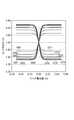
ここで、この回路40が有する問題点について説明する。図6は、図5に示された回路40の静特性を示すグラフである。図6の縦軸はトランジスタ42a及び43bのコレクタ出力(すなわち出力信号電圧)を示しており、横軸はトランジスタ41a,41bのベース電位差(すなわち入力信号InP,InNの電位差)を示している。また、図6に示されるグラフG31〜G36はトランジスタ42aのコレクタ出力を示し、グラフG41〜G45はトランジスタ43bのコレクタ出力を示す。また、これらのグラフG31〜G36,G41〜G46のそれぞれは、相対バイアス値(CtrlP−CtrlN)を0Vから0.1Vまで0.02Vずつ変化させたときの、トランジスタ42a,43bそれぞれのコレクタ電位の変化を示している。グラフG31,G41の相対バイアス値が最も低く(0V)、グラフG36,G46の相対バイアス値が最も高い(0.1V)。また、図6では、電源線47の電源電圧値として3.3Vを仮定している。また、一実施例では、電流源44の電流値は1mAである。また、負荷抵抗45,46の大きさは例えば1kΩである。 Here, the problem of the
この回路40において、制御信号CtrlP及びCtrlNの相対バイアス値が0Vであるとき、トランジスタ42a,43bは相対的にオフモードとなり、電流源44によって生じる電流の殆どは、バイパス用のトランジスタ42b,43aを流れる。したがって、負荷抵抗45,46における電圧降下量は0に近づく。そして、トランジスタ42a,43bのバイアス電圧を相対的に大きくする(トランジスタ42a,43bをオンモードにする)と、電流源44の電流の殆どがトランジスタ42a,43bを流れる。また、トランジスタ42b,43aはオンモードに準じた状態となるので、その等価抵抗値(コレクタ−エミッタ間抵抗)は負荷抵抗値と比較して十分に小さな値となり無視できる。従って、負荷抵抗45,46における電位降下量は、図3に示した回路30と同様に、例えば電流値が1mAであり且つ抵抗値が1kΩである場合、1V(すなわち出力電圧は2.3V)となる。そして、このときの利得はクロスポイント(グラフG31〜G36とグラフG41〜G46とが互いに交差する点)での静特性の傾きで与えられるので、制御信号CtrlPが大きくなるに従って利得が増加することとなる。 In this
しかし、この回路40では、図6のグラフG31からグラフG36への変化、及びグラフG41からグラフG46への変化から明らかなように、相対バイアス値(CtrlP−CtrlN)を変化させると、出力信号となるトランジスタ42a,43bのコレクタ電位も変化してしまう。この変化はクロスポイントのシフトとなって現れるので、通信システムにこの回路40をそのまま適用すると、信号波形の歪みが生じてしまう。 However, in this
そこで、このような問題点を解決するために、前述した特許文献1によって図9に示された利得可変増幅器100が提案されている。この利得可変増幅器100では、電流加算器110及び電流分配器111を介して負荷抵抗107及び108に無効電流を流すことにより、図7に示されるようなクロスポイント不変の静特性を実現している。なお、図7の縦軸および横軸は図6と同様であり、グラフG51〜G56はトランジスタ103のコレクタ出力を示し、グラフG61〜G66はトランジスタ106のコレクタ出力を示す。また、これらのグラフG51〜G56,G61〜G66のそれぞれは、相対バイアス値を0Vから0.1Vまで0.02Vずつ変化させたときのコレクタ電位の変化を示している。グラフG51,G61の相対バイアス値が最も低く(0V)、グラフG56,G66の相対バイアス値が最も高い(0.1V)。 Therefore, in order to solve such a problem, a
また、前述した特許文献3によって図11に示された利得可変増幅器300が提案されている。この利得可変増幅器300では、トランジスタ132及び133の共通エミッタ電位をトランジスタ135によって検出し、このエミッタ電位をトランジスタ131を介して一対の差動トランジスタ101及び102の電源に反映させることで、図7と同等の特性を実現している。静特性のクロスポイントが不変となるのは、次の理由による。すなわち、クロスポイントレベルは共通エミッタ電位と対応するが、図11に示された回路300では、共通エミッタ電位すなわちクロスポイントレベルを一定値に近づけようとする帰還作用が働く。但し、図4に示された伝達特性と、図7に示された伝達特性とでは、次の点で僅かに異なる。図4に示された伝達特性では、飽和時のハイレベル及びローレベルは共通エミッタ抵抗35を変化させても不変である。すなわち、当該回路30はリミッタ回路的に動作し、クロスポイントでの伝達特性の傾き(利得に相当)のみが変化する。これに対し、図7に示された伝達特性では、クロスポイントでの傾きの変化に加え、飽和時のハイレベル及びローレベルも変化している。したがって、この回路300の動作はリミッタ回路とは異なる。厳密には、リミッタ回路的に動作するが、そのリミッタ範囲が利得に追随して変化してしまう。 Further, the
以上に述べた問題点を解決するために、本実施形態に係る利得可変差動増幅回路12では、図5に示された回路40(増幅段12Aに相当)に加えて、調整段12Bが設けられている。増幅段12Aでは、出力Vout側の負荷抵抗19を流れる電流の大きさは次の数式で表される。
但し、上の数式においてIQ6はトランジスタQ6を流れる電流量であり、IQ9はトランジスタQ9を流れる電流量である。また、I1は電流源16a,16bによって規定される電流量であり、i1は入力信号Vinによって生じる交流成分である。また、ΔVは相対バイアス値(Vc+−Vc−)である。In the above equation, IQ6 is the amount of current flowing through the transistor Q6, and IQ9 is the amount of current flowing through the transistor Q9. I1 is a current amount defined by the
上の数式に示されるように、本実施形態の利得可変差動増幅回路12では、出力Voutに含まれる直流成分を決定するI1に関する項が、相対バイアス値ΔVによらず一定値となることがわかる。これは、利得を変化させたときに出力Voutの直流成分が変動しないことを表している。As shown in the above formula, in the variable gain
この作用を具体的に説明する。利得可変差動増幅回路12では、利得制御信号Vc+及びVc−によって、トランジスタQ3及びQ6に流れる電流(有効電流)と、トランジスタQ4及びQ5に流れる電流(無効電流)との相対的な差が決定される。有効電流量と無効電流量との和は常に一定となり、この和は、二つの電流源16a,16bそれぞれによって規定される電流量の和に等しい。This action will be specifically described. In the variable gain
調整段12BのトランジスタQ7〜Q10においては、各ベースに入力される利得制御信号Vc+及びVc−の配分が、増幅段12AのトランジスタQ3〜Q6とは逆になっている。すなわち、トランジスタQ7及びQ8からなる一つの差動回路21に注目すると、ベースに利得制御信号Vc+が入力されるトランジスタQ7は有効電流を提供するが、そのコレクタは電源線20(電源電圧Vcc)に直接接続されている。一方、ベースに利得制御信号Vc−が入力されるトランジスタQ8は無効電流を提供するが、そのコレクタはトランジスタQ3のコレクタに接続されており、無効電流は負荷抵抗18を通過する。すなわち、負荷抵抗18には、トランジスタQ3による有効電流とトランジスタQ7による無効電流との何れか一方が常に流れており、その電圧降下は常に一定となる。In the transistor Q7~
図8は、利得可変差動増幅回路12の静特性を示すグラフである。図8の縦軸はトランジスタQ3及びQ6のコレクタ出力(すなわち出力信号電圧)を示しており、横軸はトランジスタQ1,Q2のベース電位差(すなわち入力信号Vinの正電位側と負電位側との電位差)を示している。また、図8に示されるグラフG71〜G76はトランジスタQ3のコレクタ出力を示し、グラフG81〜G86はトランジスタQ6のコレクタ出力を示す。また、これらのグラフG71〜G76,G81〜G86のそれぞれは、相対バイアス値(Vc+−Vc−)を0Vから0.1Vまで0.2Vずつ変化させたときの、トランジスタQ3,Q6それぞれのコレクタ電位の変化を示している。グラフG71,G81の相対バイアス値が最も低く(0V)、グラフG76,G86の相対バイアス値が最も高い(0.1V)。また、図8では、電源線20の電源電圧値として3.3Vを仮定している。また、一実施例では、電流源16a,16bの電流値はそれぞれ0.5mAである。また、負荷抵抗18,19の大きさは例えば1kΩである。FIG. 8 is a graph showing the static characteristics of the variable gain
図8に示される静特性では、図7に示された静特性と比較して、ハイレベルとローレベルとの間の変化幅が大きくなっている。これは、図7に示された静特性を有する回路においては、抵抗を介して無効電流を負荷抵抗に戻しているので、抵抗による電圧降下の影響が現れているからである。図9に示された回路100のトランジスタ103から見た負荷回路は、通常の負荷抵抗107と、無効電流供給のための抵抗とからなる並列回路である。したがって、この無効電流供給用抵抗の値を小さくすると、差動回路全体の利得を減少させることとなり、この値を小さくすることには制限がある。本実施形態の利得可変差動増幅回路12では、トランジスタQ8及びQ9のコレクタが負荷抵抗18及び19にそれぞれ直接接続されているので、トランジスタQ3及びQ6から見たこれらのトランジスタQ8及びQ9のコレクタのインピーダンスは、数kΩ程度は十分に確保され、回路動作に与える影響は少ない。更に、下記のように抵抗による電位降下を考慮しなければならず、電源電圧Vccの低減化の妨げとなる。すなわち、電流加算器111は、電流を加算するためには抵抗が必須素子となり、この抵抗に流れる電流により電位降下が生ずる。電源109はこの電流加算器111を正常に動作させるためには、この電位降下分だけその設定電位を高くしなければならず、低消費電力化、低電圧化の妨げとなる。 In the static characteristic shown in FIG. 8, the range of change between the high level and the low level is larger than the static characteristic shown in FIG. This is because, in the circuit having the static characteristics shown in FIG. 7, the reactive current is returned to the load resistance via the resistor, so that the influence of the voltage drop due to the resistance appears. The load circuit viewed from the
ここで、トランジスタQ3〜Q6を含む増幅段12Aに含まれる電流源16a,16bが規定する電流量I1と、トランジスタQ7〜Q10を含む調整段12Bに含まれる二つの差動回路21,22それぞれの電流源23,24の電流量I2との比(I2/I1)は1/2であることが好ましい。この比が1/2から大きくずれると、図8に示される伝達特性が得られず、クロスポイントが制御信号Vcに追随して変化し、かつ、ハイレベル及びローレベルが、クロスポイントに対して対称とはならないからである。 Here, the current amount I1 defined by the
また、本実施形態の利得可変差動増幅回路12においては、差動トランジスタQ1及びQ2のエミッタ間に抵抗17が接続され、また、二つの電流源16a及び16bそれぞれが差動トランジスタQ1及びQ2それぞれに接続されているが、当該構成は、エミッタ同士が直接接続され、単一の電流源にて駆動されるような構成であってもよい。エミッタ間に挿入された抵抗17は、図3に示された回路30の抵抗35と同様に、差動回路の基本利得を調整するためのものである。この抵抗17の値により設定された利得が、この差動回路の最大利得となり、利得制御信号Vcの電圧値を調整することで、利得をこの最大利得から低下させることができる。 In the variable gain
以上に説明したように、本実施形態の利得可変差動増幅回路12によれば、利得を変化させた場合に、出力電圧に含まれる直流成分の変動(すなわち、クロスポイントの変動)を好適に抑えることができる。 As described above, according to the variable gain
なお、本実施形態の利得可変差動増幅回路12は、更に、以下に述べる効果を奏することができる。すなわち、特許文献2の第3図に示された回路では、利得を可変させるために分流された電流信号I5,I6を加算することで交流成分をキャンセルして直流成分のみとし、電流I8によってトランジスタのエミッタ電位(差動回路の電源電圧)を補正し、出力電圧の直流成分を安定させている。この回路では、差動増幅器に印加される電源電圧に加え、抵抗およびトランジスタに印加される電圧が別途必要となり、低電源電圧回路の実現が困難である。更に、トランジスタの温度依存性によって、出力電圧の直流成分も温度に依存してしまう。 Note that the variable gain
また、特許文献1の第1図に示された回路では、分流電流を加算した直流電流を、電流分配器を用いて負荷抵抗に流すことにより出力電圧の直流成分を安定化させている。この場合、差動増幅器には電源電圧を直接印加することができるので、電流加算器及び電流分配器に大きな電源電圧を必要としない限り、低電源電圧での動作が可能となる。しかし、出力端子に接続される電流分配器の出力インピーダンスが十分大きいことが必要であり、低電源電圧回路の実現は容易ではない。 Further, in the circuit shown in FIG. 1 of Patent Document 1, the DC component of the output voltage is stabilized by flowing a DC current obtained by adding the shunt current to a load resistor using a current distributor. In this case, since a power supply voltage can be directly applied to the differential amplifier, an operation with a low power supply voltage is possible unless a large power supply voltage is required for the current adder and the current distributor. However, it is necessary that the output impedance of the current distributor connected to the output terminal is sufficiently large, and it is not easy to realize a low power supply voltage circuit.
これらの従来技術と比較して、本実施形態の利得可変差動増幅回路12によれば、電源線20(電源電圧Vcc)以外に別途必要な電源電圧はなく、低電源電圧回路を好適に実現できる。 Compared with these conventional techniques, according to the variable gain
10…光受信装置、10a…入力端子、10b…出力端子、12,13…利得可変差動増幅回路、12A…増幅段、12B…調整段、13…第1の差動回路、14…第2の差動回路、15…第3の差動回路、16a,16b…第1の電流源、17…抵抗、18,19…負荷抵抗、20…電源線、21…第4の差動回路、22…第5の差動回路、23…第2の電流源、24…第3の電流源、26…振幅検出回路、27…利得制御回路、28…差動増幅器、29…オフセット補償回路、PD…フォトダイオード、Vc…利得制御信号、Vin…入力信号。 DESCRIPTION OF
Claims (5)
Translated fromJapanese前記増幅段は、一方の電流端子が互いに接続された一対のトランジスタ(Q1,Q2)を含み、該一対のトランジスタ(Q1,Q2)の制御端子に相補的な入力信号を受ける第1の差動回路、一方の電流端子が互いに接続された一対のトランジスタ(Q3,Q4)を含む第2の差動回路、一方の電流端子が互いに接続された一対のトランジスタ(Q5,Q6)を含む第3の差動回路、及び前記一対のトランジスタ(Q1,Q2)の前記一方の電流端子に接続された第1の電流源を有し、
前記一対のトランジスタ(Q3,Q4)の前記一方の電流端子が前記一対のトランジスタ(Q1,Q2)のうち一方の前記第1のトランジスタ(Q1)の他方の電流端子に接続されており、
前記一対のトランジスタ(Q5,Q6)の前記一方の電流端子が前記一対のトランジスタ(Q1,Q2)のうち他方の前記第1のトランジスタ(Q2)の他方の電流端子に接続されており、
正負2つの信号からなる互いに相補的な制御信号のうち一方の制御信号が前記トランジスタ(Q3,Q6)の制御端子に入力され、他方の制御信号が前記トランジスタ(Q4,Q5)の制御端子に入力され、
前記トランジスタ(Q3,Q6)の他方の電流端子が負荷抵抗を介して電源線に接続されており、前記トランジスタ(Q4,Q5)の他方の電流端子が前記電源線に直接接続されており、
前記調整段は、一方の電流端子が互いに接続された一対のトランジスタ(Q7,Q8)を含む第4の差動回路、前記一対のトランジスタ(Q7,Q8)の前記一方の電流端子に接続された第2の電流源、一方の電流端子が互いに接続された一対のトランジスタ(Q9,Q10)を含む第5の差動回路、及び前記一対のトランジスタ(Q9,Q10)の前記一方の電流端子に接続された第3の電流源を有し、
前記一方の制御信号が前記トランジスタ(Q7,Q10)の制御端子に入力され、前記他方の制御信号が前記トランジスタ(Q8,Q9)の制御端子に入力され、
前記トランジスタ(Q7,Q10)の他方の電流端子が前記電源線に直接接続されており、前記トランジスタ(Q8,Q9)の他方の電流端子が前記負荷抵抗を介して前記電源線に接続されている
ことを特徴とする、利得可変差動増幅回路。A gain variable differential amplifier circuit comprising an amplification stage and a regulation stage,
The amplification stage includes a pair of transistors (Q1, Q2) having one current terminal connected to each other, and a first differential receiving a complementary input signal at a control terminal of the pair of transistors (Q1, Q2). Circuit, a second differential circuit including a pair of transistors (Q3, Q4) with one current terminal connected to each other, a third differential circuit including a pair of transistors (Q5, Q6) with one current terminal connected to each other A differential circuit, and a first current source connected to the one current terminal of the pair of transistors (Q1, Q2);
The one current terminal of the pair of transistors (Q3, Q4) is connected to the other current terminal of the first transistor (Q1) of the pair of transistors (Q1, Q2);
The one current terminal of the pair of transistors (Q5, Q6) is connected to the other current terminal of the other first transistor (Q2) of the pair of transistors (Q1, Q2);
One of the complementary control signals consisting of two positive and negative signals is input to the control terminal of the transistor (Q3, Q6), and the other control signal is input to the control terminal of the transistor (Q4, Q5). And
The other current terminal of the transistor (Q3, Q6) is connected to a power supply line via a load resistor, and the other current terminal of the transistor (Q4, Q5) is directly connected to the power supply line,
The adjustment stage is connected to the one current terminal of the pair of transistors (Q7, Q8), a fourth differential circuit including a pair of transistors (Q7, Q8) having one current terminal connected to each other. Connected to the second current source, a fifth differential circuit including a pair of transistors (Q9, Q10) having one current terminal connected to each other, and the one current terminal of the pair of transistors (Q9, Q10) A third current source connected,
The one control signal is input to the control terminal of the transistor (Q7, Q10), the other control signal is input to the control terminal of the transistor (Q8, Q9),
The other current terminal of the transistor (Q7, Q10) is directly connected to the power supply line, and the other current terminal of the transistor (Q8, Q9) is connected to the power supply line via the load resistor. A variable gain differential amplifier circuit characterized by that.
Priority Applications (2)
| Application Number | Priority Date | Filing Date | Title |
|---|---|---|---|
| JP2010163005AJP2012028859A (en) | 2010-07-20 | 2010-07-20 | Variable gain differential amplifier circuit |
| US13/180,752US8816772B2 (en) | 2010-07-20 | 2011-07-12 | Differential amplifier with function of variable gain and optical receiver implemented with the same |
Applications Claiming Priority (1)
| Application Number | Priority Date | Filing Date | Title |
|---|---|---|---|
| JP2010163005AJP2012028859A (en) | 2010-07-20 | 2010-07-20 | Variable gain differential amplifier circuit |
Publications (1)
| Publication Number | Publication Date |
|---|---|
| JP2012028859Atrue JP2012028859A (en) | 2012-02-09 |
Family
ID=45492810
Family Applications (1)
| Application Number | Title | Priority Date | Filing Date |
|---|---|---|---|
| JP2010163005APendingJP2012028859A (en) | 2010-07-20 | 2010-07-20 | Variable gain differential amplifier circuit |
Country Status (2)
| Country | Link |
|---|---|
| US (1) | US8816772B2 (en) |
| JP (1) | JP2012028859A (en) |
Cited By (1)
| Publication number | Priority date | Publication date | Assignee | Title |
|---|---|---|---|---|
| US9608581B2 (en) | 2015-03-27 | 2017-03-28 | Sumitomo Electric Industries, Ltd. | Differential amplifier |
Families Citing this family (3)
| Publication number | Priority date | Publication date | Assignee | Title |
|---|---|---|---|---|
| JP6107103B2 (en)* | 2012-12-11 | 2017-04-05 | 富士通株式会社 | Amplifier and optical receiver |
| JP2018113520A (en)* | 2017-01-10 | 2018-07-19 | 住友電気工業株式会社 | Gain-variable differential amplifier circuit |
| KR20220125102A (en) | 2021-03-04 | 2022-09-14 | 삼성전자주식회사 | Interface circuit including variable impedence circuit and operating method thereof |
Citations (2)
| Publication number | Priority date | Publication date | Assignee | Title |
|---|---|---|---|---|
| JPH05218767A (en)* | 1992-01-28 | 1993-08-27 | Nec Corp | Variable gain amplifier circuit |
| JP2006157141A (en)* | 2004-11-25 | 2006-06-15 | Sharp Corp | Variable gain amplifier circuit, transmitter and receiver |
Family Cites Families (4)
| Publication number | Priority date | Publication date | Assignee | Title |
|---|---|---|---|---|
| JPS61219208A (en) | 1985-03-25 | 1986-09-29 | Hitachi Ltd | variable gain amplifier |
| JPS62245810A (en) | 1986-04-18 | 1987-10-27 | Fujitsu Ltd | Dc level stabilizing circuit |
| JPH01133403A (en) | 1987-11-19 | 1989-05-25 | Furukawa Electric Co Ltd:The | Automatic gain-variable amprifier |
| US6657494B2 (en)* | 2001-09-28 | 2003-12-02 | International Business Machines Corporation | Variable gain mixer-amplifier with fixed DC operating voltage level |
- 2010
- 2010-07-20JPJP2010163005Apatent/JP2012028859A/enactivePending
- 2011
- 2011-07-12USUS13/180,752patent/US8816772B2/enactiveActive
Patent Citations (2)
| Publication number | Priority date | Publication date | Assignee | Title |
|---|---|---|---|---|
| JPH05218767A (en)* | 1992-01-28 | 1993-08-27 | Nec Corp | Variable gain amplifier circuit |
| JP2006157141A (en)* | 2004-11-25 | 2006-06-15 | Sharp Corp | Variable gain amplifier circuit, transmitter and receiver |
Cited By (1)
| Publication number | Priority date | Publication date | Assignee | Title |
|---|---|---|---|---|
| US9608581B2 (en) | 2015-03-27 | 2017-03-28 | Sumitomo Electric Industries, Ltd. | Differential amplifier |
Also Published As
| Publication number | Publication date |
|---|---|
| US8816772B2 (en) | 2014-08-26 |
| US20120018622A1 (en) | 2012-01-26 |
Similar Documents
| Publication | Publication Date | Title |
|---|---|---|
| JP4896547B2 (en) | Transimpedance amplifier with signal amplification circuit for adjusting power signal | |
| JP7115065B2 (en) | transimpedance amplifier | |
| US7557333B2 (en) | Optical signal receiving circuit and optical signal receiving apparatus | |
| CN105393453A (en) | Apparatus and method for transimpedance amplifiers with wide input current ranges | |
| JPS615608A (en) | Wide band, variable gain, differential input direct couplingamplifier | |
| US6879217B2 (en) | Triode region MOSFET current source to bias a transimpedance amplifier | |
| US7319220B2 (en) | Trans-impedance amplifier with offset current | |
| US6933786B1 (en) | Amplifier circuit and method | |
| US7253685B2 (en) | Class AB amplifier having adjustable quiescent current and output current | |
| CN113507270A (en) | Variable gain amplifier | |
| US20050264363A1 (en) | Temperature compensated on-chip bias circuit for linear RF HBT power amplifiers | |
| US7728669B2 (en) | Output stage circuit and operational amplifier thereof | |
| KR20090034793A (en) | Multiplier-transimpedance amplifier combination with input common-mode feedback | |
| JP2012028859A (en) | Variable gain differential amplifier circuit | |
| US8552802B2 (en) | Amplifying circuit and current-voltage conversion circuit | |
| JP4361087B2 (en) | Preamplifier | |
| US7683715B2 (en) | Feedback biasing technique for a stage of an amplifier that uses a feedback control loop having low gain | |
| US6781462B2 (en) | Power amplifier | |
| KR20120058400A (en) | Image signal output circuit | |
| US6664912B1 (en) | Preamplifier with improved CMRR and temperature stability and associated amplification method | |
| CN110546883A (en) | Transimpedance amplifier circuit | |
| US9608581B2 (en) | Differential amplifier | |
| CN208782782U (en) | Fully differential transimpedance amplifier circuit and communication device | |
| JP4867066B2 (en) | Amplifier circuit | |
| US6469578B1 (en) | Differential current mode gain stage and methods of using the same |
Legal Events
| Date | Code | Title | Description |
|---|---|---|---|
| A621 | Written request for application examination | Free format text:JAPANESE INTERMEDIATE CODE: A621 Effective date:20130718 | |
| A977 | Report on retrieval | Free format text:JAPANESE INTERMEDIATE CODE: A971007 Effective date:20131227 | |
| A131 | Notification of reasons for refusal | Free format text:JAPANESE INTERMEDIATE CODE: A131 Effective date:20140114 | |
| A02 | Decision of refusal | Free format text:JAPANESE INTERMEDIATE CODE: A02 Effective date:20140603 |