Movatterモバイル変換


[0]ホーム

URL:


JP2012028365A - Power storage device - Google Patents

Power storage device
Download PDF

Info

Publication number
JP2012028365A
JP2012028365AJP2010162503AJP2010162503AJP2012028365AJP 2012028365 AJP2012028365 AJP 2012028365AJP 2010162503 AJP2010162503 AJP 2010162503AJP 2010162503 AJP2010162503 AJP 2010162503AJP 2012028365 AJP2012028365 AJP 2012028365A
Authority
JP
Japan
Prior art keywords
frame
electrode
pair
power storage
storage device
Prior art date
Legal status (The legal status is an assumption and is not a legal conclusion. Google has not performed a legal analysis and makes no representation as to the accuracy of the status listed.)
Pending
Application number
JP2010162503A
Other languages
Japanese (ja)
Inventor
Teruhisa Miura
照久 三浦
Susumu Nomoto
進 野本
Current Assignee (The listed assignees may be inaccurate. Google has not performed a legal analysis and makes no representation or warranty as to the accuracy of the list.)
Panasonic Corp
Original Assignee
Panasonic Corp
Priority date (The priority date is an assumption and is not a legal conclusion. Google has not performed a legal analysis and makes no representation as to the accuracy of the date listed.)
Filing date
Publication date
Application filed by Panasonic CorpfiledCriticalPanasonic Corp
Priority to JP2010162503ApriorityCriticalpatent/JP2012028365A/en
Publication of JP2012028365ApublicationCriticalpatent/JP2012028365A/en
Pendinglegal-statusCriticalCurrent

Links

Images

Classifications

Landscapes

Abstract

Translated fromJapanese

【課題】本発明は低抵抗化に優れた蓄電装置を提供することを目的とする。
【解決手段】本発明における蓄電装置は、シート状の正極2および負極3の間にセパレータを介在させて積層され、正極2と負極3のそれぞれ対向する2箇所に形成された電極を引き出すリード部2c、3cをそれぞれ備えた素子1と、この素子1の内部に含浸された電解質と、一対のリード部3cに夫々接合された一対の接続部5aを有した第1フレーム5と、一対のリード部2cに夫々接合された一対の接続部6aを有した第2フレーム6とを少なくとも備え、これにより、素子1から第1フレーム5および第2フレーム6によって、それぞれ2箇所から引き出された電極が集約されて引き出されるため、素子1と第1フレーム5および第2フレーム6との間における接触接続抵抗を低減させることができ、蓄電装置として出力特性を高めることができる。
【選択図】図1
An object of the present invention is to provide a power storage device that is excellent in resistance reduction.
A power storage device according to the present invention is formed by stacking a separator between a sheet-like positive electrode 2 and a negative electrode 3 and pulling out electrodes formed at two opposing positions of the positive electrode 2 and the negative electrode 3, respectively. A first frame 5 having a pair of connection portions 5a respectively joined to a pair of lead portions 3c, an electrolyte impregnated inside the device 1; a pair of leads; At least a second frame 6 having a pair of connection portions 6a respectively joined to the portion 2c, whereby the electrodes drawn out from two locations by the first frame 5 and the second frame 6 from the element 1 respectively. Since they are aggregated and pulled out, the contact connection resistance between the element 1 and the first frame 5 and the second frame 6 can be reduced, and the output characteristics of the power storage device are high. Rukoto can.
[Selection] Figure 1

Description

Translated fromJapanese

本発明は各種電子機器、ハイブリッド自動車や燃料電池車のバックアップ電源用や回生用、あるいは電力貯蔵用等に使用される蓄電装置に関するものである。  The present invention relates to a power storage device used for backup power source, regeneration, or power storage of various electronic devices, hybrid vehicles, and fuel cell vehicles.

従来から、機器の動作時には、使用されるエネルギーの一部が熱エネルギー等としてその機器から不必要に消費されるエネルギーとなっている。この消費されるエネルギーを、電気エネルギーとして一旦、蓄電素子に貯蔵して必要な際に再利用することにより、消費されるエネルギーを低減し、効率化することが考えられている。  Conventionally, during operation of a device, part of the energy used is energy that is unnecessarily consumed from the device as heat energy or the like. It has been considered that the consumed energy is temporarily stored as electric energy in an electric storage element and reused when necessary, thereby reducing the consumed energy and improving the efficiency.

この際に、機器の動作に必要なエネルギーを必要な出力で取り出すことが出来る蓄電素子が必須となる。その蓄電素子の候補には、大別してキャパシタと二次電池の2種類がある。  At this time, an energy storage element that can extract energy necessary for operation of the device with a necessary output is essential. There are roughly two types of storage element candidates: capacitors and secondary batteries.

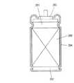
図9は従来のキャパシタの一例として示した電気二重層キャパシタの各電極の取出し方法を示した正面断面図である。  FIG. 9 is a front sectional view showing a method for taking out each electrode of an electric double layer capacitor shown as an example of a conventional capacitor.

素子200は互いに対向した帯状の正極および負極と、これら正極と負極との間に介在するセパレータからなる。  Theelement 200 includes strip-shaped positive and negative electrodes facing each other and a separator interposed between the positive and negative electrodes.

これら正極と負極は夫々、一端辺に電極部が形成されていない引き出し電極部201、202が形成されており、これら引き出し電極部201、202は互いに突出するようにずれて対向している。そして、これら引き出し電極部201、202が夫々、巻回軸方向両端部を形成するように前記正極、負極、ならびにセパレータを巻回して素子200を形成している。  Each of the positive electrode and the negative electrode is formed withlead electrode portions 201 and 202 in which no electrode portion is formed on one end side, and thelead electrode portions 201 and 202 face each other so as to protrude from each other. Then, theelement 200 is formed by winding the positive electrode, the negative electrode, and the separator so that thelead electrode portions 201 and 202 respectively form both ends in the winding axis direction.

この正極の引き出し電極部201は、金属製の端子板203と溶接などにより接合され、この端子板203から外部回路へと正極が引き出されていく。  Thelead electrode portion 201 of the positive electrode is joined to themetal terminal plate 203 by welding or the like, and the positive electrode is drawn out from theterminal plate 203 to an external circuit.

また、負極の引き出し電極部202は、有底筒状の金属ケース204の内底面と外底面などからの溶接により接合され、金属ケース204の外表面から負極が外部回路へと引き出されていく。  The negativeelectrode electrode portion 202 is joined by welding from the inner bottom surface and the outer bottom surface of the bottomedcylindrical metal case 204, and the negative electrode is drawn out from the outer surface of themetal case 204 to an external circuit.

そして、この端子板203の表面と金属ケース204は内面とが接触しないように、この間に絶縁テープ(図示なし)などを介在させている。  An insulating tape (not shown) or the like is interposed between the surface of theterminal plate 203 and themetal case 204 so that the inner surface does not contact the inner surface.

このように夫々の電極を取り出すことによって、端子板203や金属ケース204のような引き出し端子の役割をする部材と素子200との接続面積を増やすことができるため、キャパシタ内部における低抵抗化を図ることができる。  By taking out the respective electrodes in this way, the connection area between theelement 200 serving as a lead terminal such as theterminal plate 203 and themetal case 204 and theelement 200 can be increased, so that the resistance inside the capacitor is reduced. be able to.

なお、この出願に関する先行技術文献情報として、例えば特許文献1が知られている。  As prior art document information relating to this application, for example,Patent Document 1 is known.

特開2007−258414号公報JP 2007-258414 A

確かに、上記電気二重層キャパシタのように従来の蓄電装置は、上記引き出し電極部201、202のような電極未形成部からそれぞれの電極を引き出すことにより、電極の集電抵抗を減少させるとともに、この電極未形成部を端子板の底面または外装ケースの内底面へ直接接合させることにより、素子と端子板および外装ケースとの接続面積を増やし低抵抗化を図ってきた。  Certainly, the conventional power storage device, such as the electric double layer capacitor, reduces the current collecting resistance of the electrode by pulling out each electrode from the electrode-unformed part such as thelead electrode parts 201 and 202, By directly joining the electrode-unformed portion to the bottom surface of the terminal plate or the inner bottom surface of the outer case, the connection area between the element, the terminal plate and the outer case has been increased to reduce the resistance.

しかしながら、瞬時により多くのエネルギーを要する電子機器に搭載される蓄電装置については、上記電気二重層キャパシタの構成による低抵抗化に留まらず、更なる低抵抗化による出力密度の向上が求められている。  However, for power storage devices mounted on electronic devices that require more energy instantaneously, there is a demand not only for lowering the resistance by the configuration of the electric double layer capacitor but also for improving the output density by further lowering the resistance. .

そこで、本発明は低抵抗化によって出力特性が向上した蓄電装置を提供することを目的とする。  In view of the above, an object of the present invention is to provide a power storage device whose output characteristics are improved by reducing resistance.

上記課題に対して本発明における蓄電装置は、シート状の一対の電極の間にセパレータを介在させて積層され、外周面の対向する2箇所に形成されて一方の電極から電極を引き出す第1引出部と、この第1電極引出部を除いた外周面の対向する2箇所に形成されて他方の電極から電極を引き出す第2電極引出部を備えた素子と、この素子の内部に含まれた電解質と、前記素子に形成された一対の第1電極引出部に夫々接合された一対の接続部を有した第1フレームと、前記素子に形成された一対の第2電極引出部に夫々接合された一対の接続部を有した第2フレームとを少なくとも備えたことを特徴としている。  In order to solve the above-described problem, the power storage device according to the present invention is laminated with a separator interposed between a pair of sheet-like electrodes, and is formed at two opposing positions on the outer peripheral surface to draw out the electrode from one electrode. And an element including a second electrode lead portion formed at two opposing positions on the outer peripheral surface excluding the first electrode lead portion and pulling out the electrode from the other electrode, and an electrolyte contained in the element And a first frame having a pair of connection portions respectively joined to a pair of first electrode lead portions formed on the element, and a pair of second electrode lead portions formed on the element. And a second frame having a pair of connection portions.

この構成により本発明の蓄電装置は、帯状である電極体の一端辺から電流を取り出す従来の方法と比べて、電極の集電抵抗を半減させることができる。  With this configuration, the power storage device of the present invention can halve the current collecting resistance of the electrode as compared with the conventional method of taking out current from one end of the belt-like electrode body.

さらに、立方体である同じ空間に素子を可能な限り納める場合では、約2.55倍の接続面積を設けることができる。従って、各フレームと素子との間の接続抵抗を大幅に低減させることができ、より低抵抗な製品特性の発現が可能となり蓄電装置として出力特性を高めることができるものである。  Further, in the case where elements are accommodated as much as possible in the same space which is a cube, a connection area of about 2.55 times can be provided. Accordingly, the connection resistance between each frame and the element can be greatly reduced, and the product characteristics with lower resistance can be developed, and the output characteristics of the power storage device can be enhanced.

本発明の実施例1における電気二重層キャパシタを示した分解斜視図1 is an exploded perspective view showing an electric double layer capacitor in Example 1 of the present invention.本発明の実施例1における電気二重層キャパシタを示した上面断面図FIG. 3 is a top sectional view showing the electric double layer capacitor in Example 1 of the present invention.本発明の実施例1における電気二重層キャパシタを抜粋して示した正面断面図Front sectional drawing which extracted and showed the electric double layer capacitor in Example 1 of the present invention本発明の実施例1における電気二重層キャパシタを示した斜視図The perspective view which showed the electric double layer capacitor in Example 1 of this invention本発明の実施例1における電気二重層キャパシタに用いられる一方の電極の集電の様子を示した分解図The exploded view which showed the mode of the current collection of one electrode used for the electric double layer capacitor in Example 1 of this invention本発明の実施例2における電気二重層キャパシタに用いられる負極と第1フレームが当接する様子を抜粋して示したイメージ図The image figure which extracted and showed a mode that the negative electrode used for the electric double layer capacitor in Example 2 of this invention and a 1st flame | frame contact | abut本発明の実施例3における電気二重層キャパシタに用いられる素子を積層する様子を示した分解斜視図The exploded perspective view which showed a mode that the element used for the electric double layer capacitor in Example 3 of this invention was laminated | stacked(a)本発明の実施例3における電気二重層キャパシタに用いられる素子と第1フレームと第2フレームを示した上面断面図、(b)同実施例1における電気二重層キャパシタに用いられる素子を示した上面断面図(A) Top sectional view showing the element used in the electric double layer capacitor in Example 3 of the present invention and the first frame and the second frame, (b) Element used in the electric double layer capacitor in Example 1 Top view cross section shown従来の蓄電装置の一例である電気二重層キャパシタを示した正面断面図Front sectional view showing an electric double layer capacitor as an example of a conventional power storage device(a)従来の蓄電装置に用いられる素子を示した斜視図、(b)同素子を分解して一方の電極箔の一部を抜粋して示した分解図(A) The perspective view which showed the element used for the conventional electrical storage apparatus, (b) The exploded view which decomposed | disassembled the element and extracted and showed a part of one electrode foil

以下に図面を用いて本発明の実施例1および請求項1〜3、5〜12に記載の発明について説明を行うが、下記の内容に限定されない。  Hereinafter, the first embodiment of the present invention and the inventions described inclaims 1 to 3 and 5 to 12 will be described with reference to the drawings. However, the present invention is not limited to the following contents.

また、以下の本発明における蓄電装置の説明において、蓄電装置の一例として電気二重層キャパシタを用いて説明を行うが、本発明における蓄電装置は上記電気二重層キャパシタに限定されない。  In the following description of the power storage device in the present invention, an electric double layer capacitor is used as an example of the power storage device, but the power storage device in the present invention is not limited to the above electric double layer capacitor.

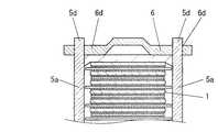
図1は本発明の実施例1における電気二重層キャパシタの分解斜視図である。  FIG. 1 is an exploded perspective view of an electric double layer capacitor according toEmbodiment 1 of the present invention.

図1において、本実施例の電気二重層キャパシタは矩形箔状である正極2および負極3を一対の電極として対向させ、この一対の電極の間にセパレータ4を介在させて積層した積層体を形成するために、一対の電極である、正極2および負極3を複数枚用意し、これらを交互に積層して正極2と負極3との間にはセパレータ4を介在させた素子1と、この素子1に含浸される電解液(図示なし)と、これら素子1および電解液を収容すると共に、素子1と電気的に接続されるコの字状の第1フレーム5および第2フレーム6から構成されている。  In FIG. 1, the electric double layer capacitor of this embodiment forms a laminated body in which apositive electrode 2 and anegative electrode 3 each having a rectangular foil shape are opposed to each other as a pair of electrodes, and a separator 4 is interposed between the pair of electrodes. In order to do this, a plurality ofpositive electrodes 2 andnegative electrodes 3 as a pair of electrodes are prepared, and these are alternately laminated, and aseparator 1 is interposed between thepositive electrode 2 and thenegative electrode 3, and thiselement 1 includes an electrolyte solution (not shown) impregnated in 1 and a U-shapedfirst frame 5 and second frame 6 that house theelement 1 and the electrolyte solution and are electrically connected to theelement 1. ing.

正極2および負極3は、例えばアルミニウム箔から成る矩形状の集電体2a、3aの表裏面上に活性炭を主成分とする電極層2b、3bを形成したものである。この電極層2b、3bを集電体2a、3aへ夫々形成する際、矩形状である集電体2a、3aの対向する一対の両端辺上には、上記電極層2b、3bを形成しない集電体表出部であるリード部2c、3cを設けるように形成する。  Thepositive electrode 2 and thenegative electrode 3 are obtained by formingelectrode layers 2b and 3b mainly composed of activated carbon on the front and back surfaces of rectangularcurrent collectors 2a and 3a made of aluminum foil, for example. When theelectrode layers 2b and 3b are formed on thecurrent collectors 2a and 3a, thecurrent collectors 2a and 3a having a rectangular shape are not formed on the pair of opposite ends of thecurrent collectors 2a and 3a. Thelead portions 2c and 3c, which are electric body exposed portions, are provided.

そして矩形状である正極2および負極3それぞれ一対のリード部2c、3cが直交するように、正極2および負極3を対向させ、その間にセパレータ4を介在させて複数の正極2および負極3、セパレータ4を積層し、素子1を構成する。その際、正極2および負極3はそれぞれのリード部2c、3cが直交関係となるように配置されているため、リード部2c、3cは互いに直交関係となるように表出している。  Thepositive electrode 2 and thenegative electrode 3 having a rectangular shape are opposed to each other such that a pair oflead portions 2c and 3c are orthogonal to each other, and a separator 4 is interposed therebetween, so that a plurality ofpositive electrodes 2 andnegative electrodes 3 and separators are interposed therebetween. 4 are stacked to form theelement 1. At that time, since thepositive electrode 2 and thenegative electrode 3 are arranged so that therespective lead portions 2c and 3c are orthogonal to each other, thelead portions 2c and 3c are exposed so as to be orthogonal to each other.

つまり、積層された素子1の積層距離を素子1の高さとすると、本実施例の電気二重層キャパシタに用いられる素子1は略十字状の柱体を形成し、四方の突出した端部はそれぞれ正極2または負極3のリード部2c、3cの集合体により構成される。  In other words, when the stacking distance of the stackedelements 1 is the height of theelement 1, theelement 1 used in the electric double layer capacitor of this embodiment forms a substantially cross-shaped column, and the projecting ends of the four sides are respectively It is comprised by the aggregate | assembly of thelead parts 2c and 3c of thepositive electrode 2 or thenegative electrode 3. FIG.

この素子1を構成するために、上記矩形状などの集電体2a、3aが方形状のものを用いた正極2および負極3を用いる場合、それぞれの電極に形成される電極層2b、3bの形状は互いに合同な正方形状とすることが好ましく、かつ、正極2の電極層2bが負極3の電極層3bとズレ少なく対向していることが望ましい。さらには、本実施例において、各電極を積層する際のズレを考慮すると、電極層3bが電極層2bの面積より大となる構成が好ましい。これは、充電において電極層2bの近傍に電解質アニオンが寄っていくが、電極層3bが対向していない場合は特に、電極層2bの近傍が酸性となり、これにより電極層2bのバインダ材料や、セパレータ4の電極層2bと対向した箇所が劣化してしまう可能性があるためである。  When thepositive electrode 2 and thenegative electrode 3 in which therectangular current collectors 2a and 3a are rectangular in order to form theelement 1, theelectrode layers 2b and 3b formed on the respective electrodes are used. The shapes are preferably congruent square shapes, and theelectrode layer 2b of thepositive electrode 2 is preferably opposed to theelectrode layer 3b of thenegative electrode 3 with little deviation. Furthermore, in the present embodiment, in consideration of a shift in stacking the electrodes, a configuration in which theelectrode layer 3b is larger than the area of theelectrode layer 2b is preferable. This is because the electrolyte anion approaches in the vicinity of theelectrode layer 2b in charging, but particularly in the case where theelectrode layer 3b is not opposed, the vicinity of theelectrode layer 2b becomes acidic, thereby the binder material of theelectrode layer 2b, This is because the portion of the separator 4 facing theelectrode layer 2b may be deteriorated.

なお、素子1を構成するセパレータ4は例えばセルロースなどの紙製のものなど正極2および負極3を絶縁するものであれば特に限定されない。  The separator 4 constituting theelement 1 is not particularly limited as long as it can insulate thepositive electrode 2 and thenegative electrode 3 such as paper made of cellulose or the like.

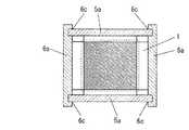
第1フレーム5は例えばコの字状のアルミニウム板から構成され、対向する一対の接続部5aとこの一対の接続部5aを中継する底面部5bから構成されている。第1フレーム5は上記素子1の一部を覆うように素子1の下側に位置し、第1フレーム5の一対の接続部5aの内面が、負極3に設けられたリード部3cにより構成された一対の集合体と当接すると共に、接合されている。つまり、リード部3cが上記第1電極引出部に該当する。  Thefirst frame 5 is composed of, for example, a U-shaped aluminum plate, and is composed of a pair ofopposing connection portions 5a and abottom surface portion 5b that relays the pair ofconnection portions 5a. Thefirst frame 5 is located on the lower side of theelement 1 so as to cover a part of theelement 1, and the inner surfaces of the pair ofconnection portions 5 a of thefirst frame 5 are constituted bylead portions 3 c provided on thenegative electrode 3. And abutted against the pair of aggregates. That is, thelead portion 3c corresponds to the first electrode lead portion.

第2フレーム6は第1フレーム5と同様に例えばコの字状のアルミニウム板から構成され、対向する平板状の一対の接続部6aとこの一対の接続部6aを中継する上面部6bから構成されている。上記素子1に対してこの第2フレーム6は上記素子1の一部を覆うように、素子1の上側に位置し、第2フレーム6の一対の接続部6aの内面が、正極2に設けられたリード部2cにより構成された一対の集合体と当接すると共に、接合されている。つまり、リード部2cが上記第2電極引出部に該当する。  Like thefirst frame 5, the second frame 6 is composed of, for example, a U-shaped aluminum plate, and is composed of a pair of opposed flat plate-like connection portions 6a and anupper surface portion 6b that relays the pair ofconnection portions 6a. ing. The second frame 6 is positioned above theelement 1 so as to cover a part of theelement 1 with respect to theelement 1, and the inner surfaces of the pair ofconnection portions 6 a of the second frame 6 are provided on thepositive electrode 2. In addition to being in contact with and joined to a pair of aggregates constituted by thelead portions 2c. That is, thelead portion 2c corresponds to the second electrode lead portion.

なお、第1フレーム5および第2フレーム6はアルミニウムの他にニッケルや鉄、銅などによって構成されていても良い。  In addition, the 1st flame |frame 5 and the 2nd flame | frame 6 may be comprised with nickel, iron, copper other than aluminum.

そして、第1フレーム5および第2フレーム6の接合および絶縁については、絶縁部材(図示なし)として例えば変性ポリプロピレンなどを当接する第1フレーム5端辺および第2フレーム6の端辺の間に介在させ、この絶縁部材へ熱を加えて融着させる、もしくは、上記変性ポリプロピレンに代えて、エポキシ系接着剤を塗布し固化させるなどが考えられるが、当接する第1フレーム5および第2フレーム6間の絶縁、封止および固定を行える手段であれば特に限定されない。  For joining and insulation between thefirst frame 5 and the second frame 6, for example, an insulating member (not shown) is interposed between the edge of thefirst frame 5 and the edge of the second frame 6 that abuts, for example, modified polypropylene. It is conceivable to apply heat to the insulating member for fusing, or to apply and solidify an epoxy adhesive instead of the modified polypropylene, but between thefirst frame 5 and the second frame 6 in contact with each other. There is no particular limitation as long as it is a means capable of insulating, sealing, and fixing.

図2は、本発明の実施例1における電気二重層キャパシタを示した上面断面図である。  FIG. 2 is a top cross-sectional view showing the electric double layer capacitor in Example 1 of the present invention.

図2のように、第1フレーム5および第2フレーム6を接合する際、さらに本実施例では、充放電時のガス発生による内圧上昇に対して機械的強度を向上させるために、第1フレーム5および第2フレーム6の接続部5a、6aにおいて、接続部6aの内面上の接続部5aの周端辺部分が当接する箇所にガイド溝6cが形成され、このガイド溝6c内面に接続部5aの周端辺部分が当接しながら第1フレーム5がガイド溝6c形成方向に沿ってスライド移動し、第2フレーム6と当接し、ガイド溝6c内部に接続部5aの周端辺部分を埋没した状態で固定されている。  As shown in FIG. 2, when thefirst frame 5 and the second frame 6 are joined, in the present embodiment, in order to improve the mechanical strength against an increase in internal pressure due to gas generation at the time of charge / discharge, thefirst frame 5 and the connectingportions 5a and 6a of the second frame 6, aguide groove 6c is formed at a location where the peripheral edge of the connectingportion 5a on the inner surface of the connectingportion 6a contacts, and the connectingportion 5a is formed on the inner surface of theguide groove 6c. Thefirst frame 5 slides along theguide groove 6c forming direction while the peripheral edge portion of the contact portion abuts, contacts the second frame 6, and the peripheral edge portion of the connectingportion 5a is buried inside theguide groove 6c. It is fixed in the state.

そして、図1のように、接続部5aの内面には同様に、接続部6aの周端辺部分が当接する箇所にガイド溝5cを形成し、ガイド溝5c内部に埋没した状態で接続部6aの周端辺部分を固定している。  As shown in FIG. 1, similarly, a guide groove 5 c is formed on the inner surface of theconnection portion 5 a at a location where the peripheral edge portion of theconnection portion 6 a abuts, and theconnection portion 6 a is buried in the guide groove 5 c. The peripheral edge part of is fixed.

この構成により、単に絶縁部材が介在して第1フレーム5および第2フレーム6を固定した構成に比べて、金属により構成された溝によって接続部5a、6aが固定されるため、格別に機械的強度が向上する。  Compared to the configuration in which thefirst frame 5 and the second frame 6 are fixed simply by interposing an insulating member, theconnection portions 5a and 6a are fixed by the grooves formed of metal, so that the mechanical structure is exceptionally mechanical. Strength is improved.

図3は、本実施例における電気二重層キャパシタを抜粋して示した正面断面図である。  FIG. 3 is a front cross-sectional view showing an excerpt of the electric double layer capacitor in this example.

加えて、図3のように本実施例では、第2フレーム6の上面部6b上において、接続部5aが当接する箇所に貫通孔6dを形成し、この接続部5aの端辺部分において貫通孔6dと対応する箇所に、貫通孔6d内に嵌合させるための突起部5dを形成し、この突起部5dを貫通孔6dへ挿入して嵌合させることにより、第1フレーム5および第2フレーム6を接合する上でさらに機械的強度を高めることができる。  In addition, as shown in FIG. 3, in this embodiment, a throughhole 6d is formed on theupper surface portion 6b of the second frame 6 at a position where the connectingportion 5a abuts, and a through hole is formed at the end portion of the connectingportion 5a. Aprojection 5d for fitting into the through-hole 6d is formed at a position corresponding to 6d, and theprojection 5d is inserted into the through-hole 6d and fitted into thefirst frame 5 and the second frame. In joining 6, the mechanical strength can be further increased.

なお、上記ガイド溝5c、6cおよび貫通孔6dと接続部5a、6aを当接させるために、その間に上記のような絶縁部材を介在させることが当然ながら必要である。上記絶縁を行うために、ガイド溝5c、6cや貫通孔6dへ絶縁部材としてゴムなどの絶縁性を有した弾性体を予め配設し、接続部5a、6aにより、圧着させる構成であってもよい。  In order to bring theguide grooves 5c and 6c and the throughhole 6d into contact with the connectingportions 5a and 6a, it is naturally necessary to interpose the insulating member as described above. In order to perform the above-described insulation, an elastic body having an insulating property such as rubber is provided in advance as an insulating member in theguide grooves 5c and 6c and the throughhole 6d, and theconnection portions 5a and 6a are crimped. Good.

図4は、本実施例における電気二重層キャパシタの斜視図である。  FIG. 4 is a perspective view of the electric double layer capacitor in the present embodiment.

また、図4のように素子1と第1フレーム5または第2フレーム6を接合する際、接続部5a、6aの外表面へ素子1を構成するリード部2c、3cの箔の端辺方向に対して垂直方向に溶接痕5e、6eがそれぞれ形成されることが好ましい。これは一度の溶接で略全ての集電体2aまたは集電体3aと接合箇所を形成することができ、本発明の蓄電装置を作製する上で生産性が高まるためである。そして、本実施例では素子1内部で電解液が分解されるなどによって生じるガスを抜くために、第2フレーム6上に自己復帰型の調圧弁7を設けた。この調圧弁7は、本実施例のように電解液を用いる場合、第1フレーム5および第2フレーム6が接合された後に第1フレーム5および第2フレーム6によって形成される素子1を収容した収容室(図示なし)の内部へ注入される電解液の注入孔(図示なし)を第1フレーム5または第2フレーム6に形成する必要があり、この注入孔を封止するように設けられていることが、部品点数などを減らせることなどから好ましい。  In addition, when theelement 1 and thefirst frame 5 or the second frame 6 are joined as shown in FIG. 4, in the direction of the edge of the foil of thelead portions 2 c and 3 c constituting theelement 1 to the outer surface of theconnection portions 5 a and 6 a. On the other hand, it is preferable that welding marks 5e and 6e are respectively formed in the vertical direction. This is because almost all thecurrent collectors 2a or current collectors 3a can be joined to each other by one-time welding, and the productivity increases in manufacturing the power storage device of the present invention. In this embodiment, a self-returning pressure regulating valve 7 is provided on the second frame 6 in order to remove gas generated due to decomposition of the electrolyte in theelement 1. When the electrolytic solution is used as in this embodiment, the pressure regulating valve 7 accommodates theelement 1 formed by thefirst frame 5 and the second frame 6 after thefirst frame 5 and the second frame 6 are joined. It is necessary to form an injection hole (not shown) for electrolyte to be injected into the interior of the storage chamber (not shown) in thefirst frame 5 or the second frame 6, and the injection hole is provided to seal the injection hole. It is preferable that the number of parts can be reduced.

また、この注入孔も電解液が上記収容室内部を流れていくことを考慮すると、第1フレーム5および第2フレーム6において、素子1が対向していない箇所、あるいは素子1が当接していない箇所に形成されていることが好ましい。  Further, in consideration of the fact that the electrolyte also flows through the inside of the accommodation chamber, the injection hole also does not contact theelement 1 in thefirst frame 5 and the second frame 6 or theelement 1 is not in contact with the injection hole. It is preferable that it is formed at a location.

これは、上記収容室において上記注入孔の近傍の空間を意図的に空けることにより、電解液の注入をよりスムーズに行うことができるためである。  This is because the electrolytic solution can be injected more smoothly by intentionally opening a space near the injection hole in the storage chamber.

この構成により、より早く素子1内部の奥深くまで電解液を含浸させることができ生産性を向上させることができる。  With this configuration, the electrolytic solution can be impregnated more deeply into theelement 1 and productivity can be improved.

このように、正極2および負極3から引き出される電極を夫々の集電体2a、3aにおいて対向する端辺部分にあたるリード部2c、3cから引き出すとともに、短絡しないようにリード部2c、3cの表出方向を直交させて素子1を形成し、それぞれのリード部2c、3cと接続する接続部5a、6aを備えた第1フレーム5および第2フレーム6によって、各電極を引き出すことによって、限られた容積の中で素子1と外部端子の役割を担う第1フレーム5および第2フレーム6の接触面積を増加させることができ、蓄電装置として素子1と第1フレーム5および第2フレーム6との間における低抵抗化を図ることができる。これは、仮に、一辺の長さをrとした立方体形状を有した同じ容積の空間に内接するように素子を収容した場合、上記一端辺から電流を取り出す従来の巻回状の素子(概算接続面積:π×r2/4)と比べて、本発明の素子1(概算接続面積:r2×2)は、一方の電極において約2.55倍の接続面積を得ることができるためである。In this way, the electrodes drawn out from thepositive electrode 2 and thenegative electrode 3 are drawn out from thelead portions 2c and 3c corresponding to the opposite end portions of the respectivecurrent collectors 2a and 3a, and thelead portions 2c and 3c are exposed so as not to be short-circuited. Theelement 1 is formed with the directions orthogonal to each other, and is limited by pulling out each electrode by thefirst frame 5 and the second frame 6 provided with theconnection portions 5a and 6a connected to therespective lead portions 2c and 3c. The contact area between theelement 1 and thefirst frame 5 and the second frame 6 serving as external terminals in the volume can be increased, and theelement 1 and thefirst frame 5 and the second frame 6 can be used as a power storage device. The resistance can be reduced. This is because if a device is accommodated so as to be inscribed in a space of the same volume having a cubic shape with the length of one side being r, a conventional spiral-shaped device (approximate connection) that takes out current from the one end side. area: compared with π × r2/4), theelement 1 of the present invention (approximately connection area: r2 × 2) is a it is possible to obtain the connection area of about 2.55 times the one of the electrodes .

さらに、上記従来の素子と比べて、本発明の素子1は各電極の集電抵抗を半減させることができる。その理由を以下に詳しく述べる。  Furthermore, as compared with the conventional element, theelement 1 of the present invention can halve the current collecting resistance of each electrode. The reason will be described in detail below.

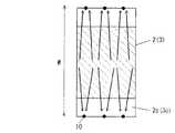
図5は本発明の蓄電装置に用いられる素子1を分解して一方の電極における接合箇所および電極内の集電方向を示した分解図である。  FIG. 5 is an exploded view of theelement 1 used in the power storage device of the present invention, showing the joint location in one electrode and the current collection direction in the electrode.

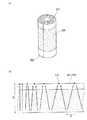
図10(a)は従来の蓄電装置に用いられる素子200を表した斜視図であり、(b)は同素子を分解して一方の電極における接合箇所および電極内の集電方向を示した分解図である。  FIG. 10A is a perspective view showing anelement 200 used in a conventional power storage device, and FIG. 10B is an exploded view showing the joint location in one electrode and the current collecting direction in the electrode by disassembling the element. FIG.

図10(a)において、従来の素子200は、巻回方向両端から電流を取り出していくため、この両端部に位置する上記引き出し電極部201、202において、上記電極引き出し部材(図示なし)と接合される。その際、図10(a)に示される矢印方向へ伸びるようにレーザー溶接などによって接合される。そして、図10(b)ように、溶接により形成された接合箇所210が形成される。この接合箇所210は、素子200が巻回状であるため、巻回軸(図示なし)により近い部分は各溶接箇所210の間隔が小さい。しかし、巻回軸から遠い部分は、同時に、集電体端部により構成される略円環の径が大きくなるため、溶接箇所210の間隔が広くなってしまう。この際、図10(b)に示される矢印のように、電極内を流れる電流は、溶接箇所210へ到達するために移動する経路が、少なくとも集電体箔の幅の距離Wの分だけ要し、加えて、接合箇所210の間隔が広い部分はその間隔の距離Dだけ移動することを要する。また、特に巻回状の素子200の最外周近傍に該当する部分は、いくら巻回軸を中心にして放射線状に溶接箇所を増やしても、素子200最外周近傍に位置する接合箇所210の間隔を狭めることは難しい。  In FIG. 10A, since theconventional element 200 takes out current from both ends in the winding direction, it is joined to the electrode lead member (not shown) at thelead electrode portions 201 and 202 located at both ends. Is done. In that case, it joins by laser welding etc. so that it may extend in the arrow direction shown by Fig.10 (a). Then, as shown in FIG. 10 (b), ajoint location 210 formed by welding is formed. Since theelement 200 has a winding shape in the joiningportion 210, a portion closer to the winding shaft (not shown) has a small interval between thewelding portions 210. However, in the portion far from the winding axis, the diameter of the substantially circular ring formed by the current collector end portion is increased at the same time, so that the interval between thewelding locations 210 is widened. At this time, as indicated by an arrow shown in FIG. 10 (b), the current flowing through the electrode requires a path for moving to reach thewelding point 210 at least for the distance W of the width of the current collector foil. In addition, it is necessary to move the portion where the interval between thejoints 210 is wide by the distance D of the interval. In particular, the portion corresponding to the vicinity of the outermost periphery of thewound element 200 has an interval between the joiningpoints 210 located near the outermost periphery of theelement 200, no matter how many welding points are radially increased around the winding axis. It is difficult to narrow down.

上記構成に比べ、図5のように、本発明に用いられる正極2あるいは負極3は、リード部2c、3cの一対の端部に溶接箇所10を有する構成となる。これにより、例えば、図10(b)の電極の集電体箔の幅と同じ大きさに形成したとしても、各電極の両端に形成された接合箇所10へ移動しようと電極内部を流れる電流の集電経路は、矢印のように約半分になる。また、上記巻回状の素子200と異なり、本実施例における素子1は積層される各電極において、接合箇所どうしの間隔が広がることは少ないため、間隔方向に集電経路が増加することを抑えることができると共に、溶接箇所増加によって各接合箇所の間隔を狭めることが容易である。このように本発明の蓄電装置は、素子1内部における集電抵抗を大幅に低減させることができる。  Compared with the said structure, as FIG. 5 shows, thepositive electrode 2 or thenegative electrode 3 used for this invention becomes a structure which has thewelding location 10 in a pair of edge part of thelead parts 2c and 3c. Thus, for example, even if the current collector foil of FIG. 10B is formed to have the same width as that of the current collector foil, the current flowing through the electrodes in an attempt to move to thejoints 10 formed at both ends of each electrode. The current collection path is about half as shown by the arrow. In addition, unlike the above-describedwound element 200, theelement 1 in this embodiment suppresses an increase in the current collecting path in the interval direction because the gap between the joint portions is rarely widened in each stacked electrode. In addition, it is easy to reduce the interval between the joints by increasing the number of welds. As described above, the power storage device of the present invention can significantly reduce the current collecting resistance inside theelement 1.

上記のことから、蓄電装置として、出力特性を高めることができる。  From the above, output characteristics can be improved as the power storage device.

加えて、低抵抗化が図れることにより、素子1と第1フレーム5および第2フレーム6との接合箇所における発熱が抑制され、セパレータの炭化や電解液の分解などの性能劣化を抑制させることができる。  In addition, by reducing the resistance, heat generation at the junction between theelement 1 and thefirst frame 5 and the second frame 6 is suppressed, and performance deterioration such as carbonization of the separator and decomposition of the electrolyte can be suppressed. it can.

なお、本実施例に用いる電解液には、溶媒として、プロピレンカーボネート(PC)やエチレンカーボネート(EC)、ジメチルカーボネート(DMC)などのうち少なくとも一つを用いた溶媒に、電解質として例えばテトラエチルアンモニウムテトラフルオロボレート(TEABF4)や、トリエチルメチルアンモニウムテトラフルオロボレート(TEMABF4)、1−エチル−3−メチルイミダゾリウムテトラフルオロボレート(EMIBF4)、1−エチル−2、3−ジメチルイミダゾリウムテトラフルオロボレート(EDMIBF4)、1、2、3−トリメチルイミダゾリウムテトラフルオロボレート(TMIBF4)及び1、3−ジメチルイミダゾリウムテトラフルオロボレート(DMIBF4)などのうち少なくとも一つを用いることができるが、特に溶媒、電解質を限定するものではない。In addition, in the electrolytic solution used in this example, a solvent using at least one of propylene carbonate (PC), ethylene carbonate (EC), dimethyl carbonate (DMC), and the like as a solvent, for example, tetraethylammonium tetra Fluoroborate (TEABF4 ), triethylmethylammonium tetrafluoroborate (TEMAFF4 ), 1-ethyl-3-methylimidazolium tetrafluoroborate (EMIBF4 ), 1-ethyl-2,3-dimethylimidazolium tetrafluoroborate use (EDMIBF4), 1,2,3- trimethyl imidazolium tetrafluoroborate (TMIBF4) and 1,3-dimethyl-imidazolium tetrafluoroborate (DMIBF4) at least one of such Although it is Rukoto, is not particularly limited solvent, an electrolyte.

上記のように電解液として用いることに限らず、溶媒中にバインダを含ませ、ゲル状のものを用いた構成や、固体状の電解質を用いた構成であってもよい。  As described above, the present invention is not limited to use as an electrolytic solution, and a configuration in which a binder is included in a solvent and a gel-like one or a solid electrolyte is used may be used.

また、集電体2a、3aに用いられる材料は、上記のようにアルミニウムに限定されず、チタン、ジルコニウム、ハフニウム、ニオブ、タンタル、クロム、モリブデン、タングステン、マンガン、珪素、鉄、銀、鉛、ニッケル、銅、白金、金や、これらの合金を用いてもよい。  Further, the material used for thecurrent collectors 2a and 3a is not limited to aluminum as described above, and titanium, zirconium, hafnium, niobium, tantalum, chromium, molybdenum, tungsten, manganese, silicon, iron, silver, lead, Nickel, copper, platinum, gold, or an alloy thereof may be used.

また、電極層2b、3bには上記のように活性炭のような炭素材料の他に、カルボキシメチルセルロースのアンモニウム塩やポリテトラフルオロエチレンなどのバインダやアセチレンブラックなどの導電剤が含まれた方が活性炭どうしの距離の短縮や導電性を向上させることができるため、素子1としてより低抵抗化を図ることができる。  In addition to the carbon material such as activated carbon as described above, the electrode layers 2b and 3b include activated carbon that includes a binder such as ammonium salt of carboxymethyl cellulose and polytetrafluoroethylene, and a conductive agent such as acetylene black. Since the distance between the electrodes can be shortened and the conductivity can be improved, theelement 1 can have a lower resistance.

本実施例では、第1フレーム5が負極と接続し、素子1の下側に位置し、第2フレーム6が正極と接続し、素子1の上側に位置する構成を説明したが、これに限定されず、接続する電極やフレームの位置が逆であってもよい。  In the present embodiment, the configuration in which thefirst frame 5 is connected to the negative electrode and positioned on the lower side of theelement 1 and the second frame 6 is connected to the positive electrode and positioned on the upper side of theelement 1 has been described. The positions of electrodes and frames to be connected may be reversed.

以下に、図面を用いながら本発明の実施例2および請求項4に記載の発明の説明を行うが、本発明は下記の内容に限定されない。また、上記実施例1と同じ構成要素については実施例1と同じ符号を付与して説明を行う。  The invention according to the second embodiment and the fourth aspect of the present invention will be described below with reference to the drawings, but the present invention is not limited to the following contents. Further, the same components as those in the first embodiment will be described with the same reference numerals as those in the first embodiment.

図6は本実施例における電気二重層キャパシタに用いられる第1フレーム5と負極13が当接する様子を示したイメージ図である。  FIG. 6 is an image diagram showing a state in which thefirst frame 5 and thenegative electrode 13 used in the electric double layer capacitor in this embodiment are in contact with each other.

本実施例では、図6のように負極13の集電体13aの両端のリード部13cの距離が第1フレーム5の一対の接続部5aの距離より長くしている。  In this embodiment, as shown in FIG. 6, the distance between thelead portions 13 c at both ends of thecurrent collector 13 a of thenegative electrode 13 is longer than the distance between the pair ofconnection portions 5 a of thefirst frame 5.

この構成により、接続部5aの内面とリード部13cを当接させる時に、本実施例における集電体13aは、リード部13cが収まらないため、接続部5aの内面に圧接されたリード部13cどうしが折曲がって重なり合った状態(スウェージ部13d)で接続部5aの内面と当接する構成となる。  With this configuration, when the inner surface of the connectingportion 5a and thelead portion 13c are brought into contact with each other, thecurrent collector 13a in this embodiment does not fit in thelead portion 13c, so that thelead portions 13c pressed against the inner surface of the connectingportion 5a are connected to each other. Is in a state of being in contact with the inner surface of the connectingportion 5a in a state of being bent and overlapped (swage portion 13d).

この構成により本実施例における電気二重層キャパシタは、リード部3cの端部のみが当接し接合される実施例1と比べ、リード部13cの端部を押圧しながら当接するようにスウェージ部13dを形成することにより、リード部13cの端部付近の集電体13aは重なるように押し倒され、この結果第1フレーム5の接続部5aとリード部13cとの接触面積が大となり、前記スウェージ部13dにおいては集電体13aが密集した(集電体13aどうしの隙間が狭まり密度が大きい)状態となるため、レーザー溶接による集電体13aの溶断の防止や、第1フレーム5の接続部5aに孔が開くことを防止することができ、ものつくりの信頼性を向上させることができるものである。  With this configuration, the electric double layer capacitor in this embodiment has theswage portion 13d so as to abut against the end portion of thelead portion 13c while pressing the end portion of thelead portion 13c, as compared with the first embodiment in which only the end portion of thelead portion 3c abuts and is joined. By forming thecurrent collector 13a near the end of thelead portion 13c, thecurrent collector 13a is pushed down so as to overlap. As a result, the contact area between theconnection portion 5a of thefirst frame 5 and thelead portion 13c becomes large, and theswage portion 13d. Since thecurrent collector 13a is densely packed (the gap between thecurrent collectors 13a is narrowed and the density is high), thecurrent collector 13a can be prevented from being melted by laser welding, and theconnection portion 5a of thefirst frame 5 can be prevented. Opening of holes can be prevented, and the reliability of manufacturing can be improved.

また、リード部13cにおいてより容易にスウェージ部13dを形成するために、予めリード部13c上に屈曲部分(図示なし)、もしくは切り込み(図示なし)などを入れ、第2フレーム6、もしくは第1フレーム5にスライド挿入することにより得てもよいし、もしくは、上記屈曲部分、切り込みからリード部13cの端までを優先的に折り曲げるなど行ってもよい。  Further, in order to more easily form theswage portion 13d in thelead portion 13c, a bent portion (not shown) or a notch (not shown) is previously provided on thelead portion 13c, and the second frame 6 or the first frame. 5 or may be obtained by bending the bent portion or notch to the end of thelead portion 13c preferentially.

なお、リード部13cに上記屈曲部分を形成する方法として、例えば、リード部13cの所望の位置にローラー(図示なし)などを押し当てることにより、リード部13c側の電極層13bの端辺と平行方向に形成する方法などがある。  As a method of forming the bent portion in thelead portion 13c, for example, a roller (not shown) or the like is pressed against a desired position of thelead portion 13c to be parallel to the end side of theelectrode layer 13b on thelead portion 13c side. There is a method of forming in the direction.

また、リード部13cに上記切り込みを形成する方法として、例えば、リード部13cの端辺を形成するスリット加工と同時にカットローラー(図示なし)などを押し当てることでリード部13c側の電極層13bの端辺に対して平行方向にリード部13c上に形成する方法などがある。  In addition, as a method of forming the above-mentioned cut in thelead portion 13c, for example, theelectrode layer 13b on thelead portion 13c side is pressed by pressing a cut roller (not shown) at the same time as slitting for forming the end of thelead portion 13c. There is a method of forming on thelead portion 13c in a direction parallel to the end side.

なお、本実施例では負極13および接続部5aを用いて説明を行ったが、実施例1における正極2と接続部6aとの間においても同様の構成を用いて、同様にものつくりの信頼性を向上させることができるものである。  Although the present embodiment has been described using thenegative electrode 13 and the connectingportion 5a, the same structure is used between thepositive electrode 2 and the connectingportion 6a in the first embodiment, and the manufacturing reliability is also the same. Can be improved.

以下に、図面を用いて実施例3と請求項13に記載の発明について説明を行うが、以下の内容に限定されない。  The invention according to the third embodiment and the thirteenth aspect will be described below with reference to the drawings, but is not limited to the following contents.

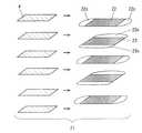
図7は本実施例における電気二重層キャパシタに用いられる素子21を形成する様子を示した分解斜視図である。  FIG. 7 is an exploded perspective view showing how theelement 21 used in the electric double layer capacitor in this embodiment is formed.

図8(a)は本実施例における電気二重層キャパシタに用いられる素子21と第1フレーム25と第2フレーム26の上面断面図であり、図8(b)は実施例1における電気二重層キャパシタに用いられる素子1の上面断面図である。  8A is a top sectional view of theelement 21, thefirst frame 25, and thesecond frame 26 used in the electric double layer capacitor in the present embodiment, and FIG. 8B is an electric double layer capacitor in the first embodiment. It is top surface sectional drawing of theelement 1 used for FIG.

図7のように、本実施例における電気二重層キャパシタは、実施例1において方形箔状であった正極2および負極3のリード部2c、3cに対して、接続部5a、6aと当接する端辺が円弧状となるようにリード部22c、23cを形成したものである。  As shown in FIG. 7, the electric double layer capacitor in this example is an end in contact with theconnection parts 5 a and 6 a with respect to thelead parts 2 c and 3 c of thepositive electrode 2 and thenegative electrode 3 that were in the shape of a rectangular foil in the first example. Leadportions 22c and 23c are formed so that the sides are arcuate.

これにより、接続部5a、6aが平板状だった実施例1に対して、本実施例の正極22および負極23に形成されたリード部22c、23cの形状に即して曲面を形成する構成となる。そして、第1フレーム5および第2フレーム6によりブロック体を形成した実施例1に対して、本実施例は、電気二重層キャパシタの側面に該当する第1フレーム25、第2フレーム26の接続部25a、26aの少なくとも一部に曲面が形成された蓄電装置を形成することができる。  Thereby, with respect to the first embodiment in which theconnection portions 5a and 6a are flat, a curved surface is formed in accordance with the shape of thelead portions 22c and 23c formed on thepositive electrode 22 and thenegative electrode 23 of the present embodiment. Become. Further, in contrast to the first embodiment in which the block body is formed by thefirst frame 5 and the second frame 6, this embodiment is a connecting portion of thefirst frame 25 and thesecond frame 26 corresponding to the side surface of the electric double layer capacitor. A power storage device in which a curved surface is formed on at least a part of 25a and 26a can be formed.

これは、これら曲面の内表面には接続部25a、26aとしてリード部22c、23cと電気的に接続した接合箇所が形成されている。この接合箇所は、本発明の蓄電装置を使用して充放電した場合、蓄電装置内部で発生した熱が内部から外部へ伝わる際に、熱の伝達経路となる。そして、蓄電装置の外表面の中で特に温度が高くなるこの接合箇所を積極的に冷却して、冷却効率を高めることができるためである。  In the inner surfaces of these curved surfaces, joint portions electrically connected to thelead portions 22c and 23c are formed asconnection portions 25a and 26a. When the power storage device according to the present invention is used for charging and discharging, the joint portion serves as a heat transfer path when heat generated inside the power storage device is transferred from the inside to the outside. This is because the joint portion where the temperature is particularly high in the outer surface of the power storage device can be actively cooled to increase the cooling efficiency.

このように接続部25a、26aに曲面が形成された本実施例における電気二重層キャパシタは、複数個並列に配置してユニットを形成し、接続部25a、26aを側面として冷媒を用いて冷却など行う場合、各本実施例の電気二重層キャパシタの並列方向に上記冷媒を流すと、冷媒は各本実施例の電気二重層キャパシタの有する接続部25a、26aの曲面に従って、この曲面の外周を覆うように通過していく。  As described above, the electric double layer capacitors in the present embodiment in which theconnection portions 25a and 26a have curved surfaces are arranged in parallel to form a unit, and theconnection portions 25a and 26a are cooled by using a refrigerant as a side surface. In the case of performing the above, when the refrigerant flows in the parallel direction of the electric double layer capacitor of each embodiment, the refrigerant covers the outer periphery of the curved surface according to the curved surfaces of the connectingportions 25a and 26a of the electric double layer capacitor of each embodiment. To pass through.

図8(b)のように、実施例1などの様にブロック体の電気二重層キャパシタを構成すると、このブロック体の電気二重層キャパシタを複数個並列させてユニットを構成する場合、容積効率を考慮して平面である各接続部5a、6aが対向し、近接するように並列させることが一般的である。このようにブロック体の電気二重層キャパシタによってユニットを構成すると、他の接続部5a、6aと対向していない接続部5a、6aの外表面が、冷媒によって優先的に冷却されることになる。これに対して、本実施例のように素子21との接合箇所が曲面である電気二重層キャパシタは、図8(a)のように、実施例1のようなブロック体の電気二重層キャパシタに比べて、側面が曲面であるため表面積が拡大し、かつ、冷媒が通過するスペースの確保が容易となるため電気二重層キャパシタの冷却性能を高めることができ、これにより、電気二重層キャパシタの信頼性を高めることができる。  As shown in FIG. 8B, when a block type electric double layer capacitor is configured as in the first embodiment or the like, when a unit is configured by arranging a plurality of block type electric double layer capacitors in parallel, volume efficiency is improved. In general, the connectingportions 5a and 6a, which are planes, face each other and are generally arranged in parallel so as to be close to each other. Thus, when a unit is comprised by the electric double layer capacitor of a block body, the outer surface of theconnection parts 5a and 6a which are not facing theother connection parts 5a and 6a will be cooled preferentially with a refrigerant | coolant. On the other hand, an electric double layer capacitor having a curved surface at the junction with theelement 21 as in the present embodiment is replaced with a block electric double layer capacitor as in the first embodiment as shown in FIG. Compared to the curved surface, the surface area is increased, and it is easy to secure a space for the refrigerant to pass through. Therefore, the cooling performance of the electric double layer capacitor can be improved. Can increase the sex.

なお、上記実施例1〜3において構成要素として説明された第1フレーム5および第2フレーム6は一対の接続部5a、6aを備えた略コの字状の金属部材であったが、この構成に限定されず、素子1の2方向の両端から各電極がそれぞれ引き出される構成に対して少なくとも一対の接続部を備え、2箇所から引き出される電極を一括して外部回路へ引き出す構成を有していれば、蓄電装置の低抵抗化という本発明の格別の効果を奏するものである。  In addition, although the1st frame 5 and the 2nd frame 6 which were demonstrated as a component in the said Examples 1-3 were the substantially U-shaped metal members provided with a pair ofconnection parts 5a and 6a, this structure It is not limited to, It has the structure which has at least a pair of connection part with respect to the structure by which each electrode is each pulled out from the both ends of theelement 1 in two directions, and pulls out the electrode pulled out from two places to an external circuit collectively Then, the special effect of the present invention, that is, lowering the resistance of the power storage device, is achieved.

従って、上記第1フレーム5または第2フレーム6の一方が有底状のケース状の金属部材であってもよく、また、第1フレーム5および第2フレーム6を外部端子としてだけ用い、素子1および電解質を収容する樹脂または金属部材などの外装体を、別途設けてもよい。  Accordingly, one of thefirst frame 5 and the second frame 6 may be a bottomed case-like metal member, and thefirst frame 5 and the second frame 6 are used only as external terminals, and theelement 1 In addition, an exterior body such as a resin or a metal member that accommodates the electrolyte may be provided separately.

しかし、これらの構成をとる場合、第1フレーム5および第2フレーム6が直接当接しないように絶縁を十分に行う必要がある。  However, when adopting these configurations, it is necessary to sufficiently insulate so that thefirst frame 5 and the second frame 6 do not directly contact each other.

なお、本発明は電気二重層キャパシタに限定されることはなく、電解質のカチオンとしてリチウムイオンを用い、負極の電極層に含まれる炭素材料、あるいはカチオンと合金化が可能である金属にリチウムを吸蔵させ、かつ、正極は電気二重層キャパシタの正極を用いて充放電を行う電気化学キャパシタや、同様に、リチウム二次電池を始めとする夫々の電極層の集電部材として金属部材を主に用いた蓄電池に応用しても上記のような蓄電装置として低抵抗化の実現という格別な効果を奏することができる。  The present invention is not limited to an electric double layer capacitor. Lithium ions are used as electrolyte cations, and lithium is occluded in a carbon material contained in the electrode layer of the negative electrode or a metal that can be alloyed with cations. The positive electrode is an electrochemical capacitor that is charged and discharged using the positive electrode of an electric double layer capacitor, and similarly, a metal member is mainly used as a current collecting member for each electrode layer such as a lithium secondary battery. Even when applied to a conventional storage battery, the power storage device as described above can achieve a special effect of realizing low resistance.

以上のように、本発明における蓄電装置は、シート状の正極および負極がセパレータを介在させた状態で積層された素子であるとともに、正極および負極が対向する両端から表出された電極引出部をそれぞれ備え、それぞれの一対である一方の電極引出部から電極を引き出す一対の第1の接続部を有した第1フレームおよび一対である他方の電極引出部から電極を引き出す一対の第2の接続部を有した第2フレームを少なくとも備えた構成であり、この一対の接続部を備えた第1フレームおよび第2フレームによって、従来それぞれの電極箔において一方から引き出された電極を、2箇所から引き出すことによって、限られた空間の中で素子の各一対の電極引出部と外部端子の役割を担う第1フレームおよび第2フレームの接触面積を増やし、蓄電装置として低抵抗化を図ることができる。  As described above, the power storage device according to the present invention is an element in which a sheet-like positive electrode and a negative electrode are stacked with a separator interposed therebetween, and an electrode lead-out portion exposed from both ends of the positive electrode and the negative electrode facing each other. A first frame having a pair of first connection portions each for providing an electrode from one electrode extraction portion that is each pair and a pair of second connection portions for extracting an electrode from the other electrode extraction portion that is a pair The first frame and the second frame having a pair of connection portions are used to pull out electrodes that have been drawn from one side in each of the conventional electrode foils from two locations. Increases the contact area between the pair of electrode lead portions of the element and the first frame and the second frame that serve as external terminals in a limited space. It can reduce the resistance as the power storage device.

本発明における蓄電装置は、シート状である各電極の対向する両端からそれぞれの電極を引き出す素子と、このシート状の電極から電極を引き出す一対の接続部を備えた第1フレームおよび第2フレームを少なくとも備え、これにより、素子から第1フレームおよび第2フレームを用いて電極を引き出す際の接触面積を増やし、低抵抗化が達成されたものである。  The power storage device according to the present invention includes a first frame and a second frame each having an element that pulls out each electrode from opposite ends of each sheet-like electrode, and a pair of connection portions that draw the electrode from the sheet-like electrode. At least, the contact area at the time of extracting an electrode from the element using the first frame and the second frame is increased, and a reduction in resistance is achieved.

従って、本発明における蓄電装置は、短時間でより多くの電力を取り出すことを要する電子機器や電気自動車などの移動体での利用が期待される。  Therefore, the power storage device according to the present invention is expected to be used in a mobile body such as an electronic device or an electric vehicle that needs to extract more power in a short time.

1、21 素子
2、22 正極
2a、3a、13a 集電体
2b、3b、13b 電極層
2c、3c、13c、22c、23c リード部
3、13、23 負極
13d スウェージ部
4 セパレータ
5、25 第1フレーム
5a、6a、25a、26a 接続部
5b 底面部
5c、6c ガイド溝
5d 突起部
5e、6e 溶接痕
6、26 第2フレーム
6b 上面部
6d 貫通孔
7 調圧弁
10 接合箇所
1, 21Element 2, 22Positive electrode 2a, 3a, 13aCurrent collector 2b, 3b,13b Electrode layer 2c, 3c, 13c, 22c,23c Lead part 3, 13, 23Negative electrode 13d Swage part 4Separator 5, 251st Frame 5a, 6a, 25a,26a Connection portion 5bBottom surface portion 5c,6c Guide groove5d Projection portion 5e, 6eWeld mark 6, 26Second frame 6bTop surface portion 6d Through hole 7Pressure regulating valve 10 Joint location

Claims (13)

Translated fromJapanese
シート状の一対の電極の間にセパレータを介在させて積層され、外周面の対向する2箇所に形成されて一方の電極から電極を引き出す第1電極引出部と、この第1電極引出部を除いた外周面の対向する2箇所に形成されて他方の電極から電極を引き出す第2電極引出部を備えた素子と、この素子の内部に含まれた電解質と、前記素子に形成された一対の第1電極引出部に夫々接合された一対の接続部を有した第1フレームと、前記素子に形成された第2電極引出部に夫々接合された一対の接続部を有した第2フレームとを少なくとも備えた蓄電装置。A pair of sheet-like electrodes are stacked with a separator interposed therebetween, and are formed at two opposing locations on the outer peripheral surface, excluding the first electrode lead-out portion that pulls out the electrode from one electrode, and excluding this first electrode lead-out portion An element having a second electrode extraction portion that is formed at two opposite positions on the outer peripheral surface and draws an electrode from the other electrode, an electrolyte contained in the element, and a pair of first electrodes formed in the element At least a first frame having a pair of connection portions respectively joined to one electrode lead portion and a second frame having a pair of connection portions respectively joined to a second electrode lead portion formed in the element. A power storage device provided.前記第1、2フレームがそれぞれ、平面部の両端をそれぞれ折り曲げて対向した一対の接続部が形成されたコの字型の金属材料から成り、これら第1、2フレームが有する夫々の接続部の位置が90度転回した状態で、かつ、互いの接続部を繋ぐ前記平面部の内面が対向するように配設され、前記第1フレームの一対の接続部が前記第1電極引出部に夫々接合されると共に、前記第2フレームの一対の接続部が前記素子の第2電極引出部に夫々接合された請求項1に記載の蓄電装置。Each of the first and second frames is made of a U-shaped metal material in which a pair of connection portions opposed to each other by bending both ends of the plane portion are formed. In a state where the position is rotated 90 degrees, the inner surfaces of the flat portions connecting the connecting portions are arranged to face each other, and the pair of connecting portions of the first frame are joined to the first electrode lead-out portions, respectively. The power storage device according to claim 1, wherein the pair of connection portions of the second frame are respectively joined to the second electrode lead-out portions of the elements.前記素子と接合された第1、2フレームの周端辺部が互いに当接して前記素子を収容する収容室が形成され、これら第1、2フレームの当接する箇所へ絶縁部が形成され、この絶縁部を介して第1、2フレームが互いに当接した請求項2に記載の蓄電装置。The peripheral edge sides of the first and second frames joined to the element are in contact with each other to form a storage chamber for storing the element, and an insulating portion is formed at a place where the first and second frames are in contact, The power storage device according to claim 2, wherein the first and second frames are in contact with each other via an insulating portion.前記第1、2フレームが互いに当接した箇所において、一方のフレームに凸部が形成されると共に、他方のフレームに凹部が形成され、前記凸部が前記凹部に挿入されて前記第1、2フレームが互いに当接した請求項3に記載の蓄電装置。At the place where the first and second frames are in contact with each other, a convex portion is formed on one frame, a concave portion is formed on the other frame, and the convex portion is inserted into the concave portion, so that the first and second frames are inserted. The power storage device according to claim 3, wherein the frames are in contact with each other.前記他方のフレームに形成された凹部がガイド溝であると共に、前記一方のフレームに形成された凸部が前記接続部の端辺であり、前記ガイド溝の内部に前記端辺の一部が埋没して当接した請求項4に記載の蓄電装置。The concave portion formed in the other frame is a guide groove, the convex portion formed in the one frame is an end side of the connection portion, and a part of the end side is buried in the guide groove. The power storage device according to claim 4, which is in contact with each other.前記第1、2フレームが互いに当接した箇所において、一方のフレームに凸部が形成されると共に、他方のフレームに貫通孔が形成され、前記凸部が前記貫通孔に嵌合されて前記第1フレームならびに第2フレームが互いに当接した請求項3に記載の蓄電装置。At the place where the first and second frames are in contact with each other, a convex portion is formed on one frame, a through hole is formed on the other frame, and the convex portion is fitted into the through hole to form the first The power storage device according to claim 3, wherein the first frame and the second frame are in contact with each other.前記素子は複数枚の前記一対の電極がその間に前記セパレータを介在させた状態で交互に積層されて構成された請求項1に記載の蓄電装置。The power storage device according to claim 1, wherein the element is configured by alternately laminating a plurality of the pair of electrodes with the separator interposed therebetween.前記一対の電極が夫々、シート状の金属から成る集電体と、この集電体の表面に形成された電極部から成り、前記正極および前記負極夫々に備えられた集電体の対向する端辺に前記電極部が形成されない一対の集電体表出部が形成され、これら一対の集電体表出部がそれぞれ、前記第1電極引出部または前記第2電極引出部である請求項1〜7いずれか一つに記載の蓄電装置。Each of the pair of electrodes is composed of a current collector made of sheet-like metal and an electrode portion formed on the surface of the current collector, and the opposite ends of the current collector provided in each of the positive electrode and the negative electrode 2. A pair of current collector exposed portions in which the electrode portions are not formed on a side are formed, and the pair of current collector exposed portions are the first electrode lead portion or the second electrode lead portion, respectively. The electrical storage apparatus as described in any one of -7.前記第1、2フレームに夫々形成された一対の接続部の対向距離が、前記一対の電極が有する集電体の電極引き出し方向両端の距離より小さい請求項8に記載の蓄電装置。The power storage device according to claim 8, wherein a facing distance between a pair of connection portions formed in the first and second frames is smaller than a distance between both ends of the current collector in the electrode drawing direction.前記一対の電極に形成された電極部に活性炭が含まれた請求項8に記載の蓄電装置。The power storage device according to claim 8, wherein activated carbon is contained in electrode portions formed on the pair of electrodes.前記一対の電極のうち負極に形成された電極部にはカチオンが吸蔵された炭素材料が含まれ、前記正極に形成された電極部にはアニオンを吸脱着する活性炭が含まれ、前記カチオンと前記アニオンからなる電解質が有機溶媒とともに電解液を構成した請求項8に記載の蓄電装置。The electrode part formed on the negative electrode of the pair of electrodes includes a carbon material in which cations are occluded, and the electrode part formed on the positive electrode includes activated carbon that absorbs and desorbs anions, and the cations and the The power storage device according to claim 8, wherein an electrolyte composed of an anion constitutes an electrolytic solution together with an organic solvent.前記電解質は溶媒に含まれて電解液を構成すると共に、前記第1フレームまたは第2フレームの前記平面部において、前記素子と当接していない箇所に貫通孔が形成された請求項2に記載の蓄電装置。3. The electrolyte according to claim 2, wherein the electrolyte is contained in a solvent to constitute an electrolytic solution, and a through-hole is formed at a location not in contact with the element in the planar portion of the first frame or the second frame. Power storage device.前記一対の電極それぞれに形成された集電体表出部の前記接続部と当接する端辺が円弧状である請求項8に記載の蓄電装置。The power storage device according to claim 8, wherein an end of the current collector exposed portion formed on each of the pair of electrodes that contacts the connection portion has an arc shape.
JP2010162503A2010-07-202010-07-20Power storage devicePendingJP2012028365A (en)

Priority Applications (1)

Application NumberPriority DateFiling DateTitle
JP2010162503AJP2012028365A (en)2010-07-202010-07-20Power storage device

Applications Claiming Priority (1)

Application NumberPriority DateFiling DateTitle
JP2010162503AJP2012028365A (en)2010-07-202010-07-20Power storage device

Publications (1)

Publication NumberPublication Date
JP2012028365Atrue JP2012028365A (en)2012-02-09

Family

ID=45780995

Family Applications (1)

Application NumberTitlePriority DateFiling Date
JP2010162503APendingJP2012028365A (en)2010-07-202010-07-20Power storage device

Country Status (1)

CountryLink
JP (1)JP2012028365A (en)

Cited By (5)

* Cited by examiner, † Cited by third party
Publication numberPriority datePublication dateAssigneeTitle
JP2017004902A (en)*2015-06-152017-01-05トヨタ自動車株式会社Manufacturing method for battery container, and battery container
JP2018045947A (en)*2016-09-162018-03-22トヨタ自動車株式会社 Stacked battery
JP2018045946A (en)*2016-09-162018-03-22トヨタ自動車株式会社 Stacked battery
JP2018045948A (en)*2016-09-162018-03-22トヨタ自動車株式会社Stacked battery
JP2022032463A (en)*2020-08-122022-02-25プライムプラネットエナジー&ソリューションズ株式会社Method of manufacturing square battery and square battery

Cited By (10)

* Cited by examiner, † Cited by third party
Publication numberPriority datePublication dateAssigneeTitle
JP2017004902A (en)*2015-06-152017-01-05トヨタ自動車株式会社Manufacturing method for battery container, and battery container
US10355252B2 (en)2015-06-152019-07-16Toyota Jidosha Kabushiki KaishaMethod for manufacturing bottomed cuboid battery container
JP2018045947A (en)*2016-09-162018-03-22トヨタ自動車株式会社 Stacked battery
JP2018045946A (en)*2016-09-162018-03-22トヨタ自動車株式会社 Stacked battery
JP2018045948A (en)*2016-09-162018-03-22トヨタ自動車株式会社Stacked battery
CN107834012A (en)*2016-09-162018-03-23丰田自动车株式会社Laminate type battery
US10446805B2 (en)2016-09-162019-10-15Toyota Jidosha Kabushiki KaishaStacked battery
JP2022032463A (en)*2020-08-122022-02-25プライムプラネットエナジー&ソリューションズ株式会社Method of manufacturing square battery and square battery
JP7285809B2 (en)2020-08-122023-06-02プライムプラネットエナジー&ソリューションズ株式会社 Prismatic battery manufacturing method and prismatic battery
US12148936B2 (en)2020-08-122024-11-19Prime Planet Energy & Solutions, Inc.Method for manufacturing angular battery, and angular battery

Similar Documents

PublicationPublication DateTitle
JP5774752B2 (en) Battery and battery pack
JP5583421B2 (en) Square sealed secondary battery and method for manufacturing square sealed secondary battery
JP4061938B2 (en) Storage element and method for manufacturing the same
JP4378657B2 (en) Battery and power supply
JP6582500B2 (en) Electricity storage element
JP5336024B1 (en) Secondary battery
JP4964350B2 (en) Electrochemical device and manufacturing method thereof
JP5258970B2 (en) Flat wound power storage device cell and flat wound power storage device module
JP5841571B2 (en) Secondary battery
JP5730321B2 (en) Lithium ion capacitor
JP2000150306A (en) Battery or capacitor current collection method
KR102394698B1 (en) battery pack
JP2004266091A (en)Film type storage device
JP2018060599A (en)Square secondary battery
JP2012028365A (en)Power storage device
JP2012060052A (en)Power storage device
JP2014203885A (en)Sealing structure of power storage device and electric double layer capacitor
JP2012059863A (en)Power storage element
WO2015186834A1 (en)Secondary battery
KR20110082966A (en) Secondary battery
JP6487716B2 (en) Power storage device and power storage module
JP2015060823A (en)Flat wound secondary battery
JP2013207026A (en)Capacitor and capacitor module using the same
JP6171395B2 (en) Power storage device and method for manufacturing power storage device
JP2012243839A (en)Electric power storage device cell and electric power storage device cell module

[8]ページ先頭

©2009-2025 Movatter.jp