JP2012023296A - Circuit board, method of manufacturing the same, substrate for suspension, suspension, suspension with element and hard disk drive - Google Patents
Circuit board, method of manufacturing the same, substrate for suspension, suspension, suspension with element and hard disk driveDownload PDFInfo
- Publication number
- JP2012023296A JP2012023296AJP2010161803AJP2010161803AJP2012023296AJP 2012023296 AJP2012023296 AJP 2012023296AJP 2010161803 AJP2010161803 AJP 2010161803AJP 2010161803 AJP2010161803 AJP 2010161803AJP 2012023296 AJP2012023296 AJP 2012023296A
- Authority
- JP
- Japan
- Prior art keywords
- wiring
- circuit board
- layer
- suspension
- wiring portion
- Prior art date
- Legal status (The legal status is an assumption and is not a legal conclusion. Google has not performed a legal analysis and makes no representation as to the accuracy of the status listed.)
- Pending
Links
Images


Landscapes
- Parts Printed On Printed Circuit Boards (AREA)
- Manufacturing Of Printed Circuit Boards (AREA)
- Manufacturing Of Printed Wiring (AREA)
Abstract
Translated fromJapaneseDescription
Translated fromJapanese本発明は、配線間隔を狭くすることができ、微細化に適した回路基板に関する。 The present invention relates to a circuit board that can narrow a wiring interval and is suitable for miniaturization.
回路基板における配線層のパターニングの方法として、いわゆるサブトラクティブ法が知られている。サブトラクティブ法は、例えば、パターニングする前の配線層(導体層)に、フォトレジストを塗布またはラミネートし、そのフォトレジストに露光および現像を行うことでレジストパターンを形成し、その後、レジストパターンから露出する導体層をエッチングすることにより、パターニングされた配線層を形成する方法である。 A so-called subtractive method is known as a method for patterning a wiring layer on a circuit board. In the subtractive method, for example, a photoresist is applied or laminated to a wiring layer (conductor layer) before patterning, and a resist pattern is formed by exposing and developing the photoresist, and then exposed from the resist pattern. In this method, a patterned wiring layer is formed by etching a conductor layer.
サブトラクティブ法は、絶縁層との密着性が良好な配線層を得ることができる反面、配線間隔が広くなり、微細化に適さないという問題がある。サブトラクティブ法の原理上、配線間隔はレジストパターンの開口寸法に依存する。配線間隔を狭くするためには、レジストパターンの開口寸法を小さくすることが有効であるが、露光の描画安定性およびレジストの解像性には限界がある。また、配線間隔を狭くするために、配線層(導体層)の厚さを小さくすることも有効であるが、配線層の厚さを小さくしすぎると、電気特性が悪化するという問題がある。なお、サブトラクティブ法には、サイドエッチングの問題もある(特許文献1、2)。 The subtractive method can obtain a wiring layer having good adhesion to the insulating layer, but has a problem that the wiring interval becomes wide and is not suitable for miniaturization. On the principle of the subtractive method, the wiring interval depends on the opening size of the resist pattern. In order to reduce the wiring interval, it is effective to reduce the opening size of the resist pattern, but there is a limit to the exposure drawing stability and the resist resolution. In order to reduce the wiring interval, it is effective to reduce the thickness of the wiring layer (conductor layer). However, if the thickness of the wiring layer is too small, there is a problem that electrical characteristics deteriorate. The subtractive method also has a problem of side etching (Patent Documents 1 and 2).
本発明は、上記問題点に鑑みてなされたものであり、配線間隔を狭くすることができ、微細化に適した回路基板を提供することを主目的とする。 The present invention has been made in view of the above problems, and a main object of the present invention is to provide a circuit board that can reduce the wiring interval and is suitable for miniaturization.
上記課題を解決するために、本発明においては、絶縁層と、上記絶縁層上に形成された配線層とを有する回路基板であって、上記配線層が、第一配線部と、上記第一配線部の側面にめっき法により形成された第二配線部とを有し、上記第一配線部および上記第二配線部の頂面の位置が一致していることを特徴とする回路基板を提供する。 In order to solve the above problems, in the present invention, a circuit board having an insulating layer and a wiring layer formed on the insulating layer, the wiring layer including a first wiring portion and the first wiring A circuit board having a second wiring portion formed by plating on a side surface of the wiring portion, and the top surfaces of the first wiring portion and the second wiring portion being aligned with each other is provided. To do.
本発明によれば、第一配線部の側面に第二配線部が形成されていることから、配線間隔を狭くすることができ、配線層の微細化に適した回路基板とすることができる。 According to the present invention, since the second wiring portion is formed on the side surface of the first wiring portion, the wiring interval can be narrowed, and a circuit board suitable for miniaturization of the wiring layer can be obtained.
上記発明においては、上記第一配線部の材料が、銅または銅合金であることが好ましい。導電性に優れているからである。 In the said invention, it is preferable that the material of said 1st wiring part is copper or a copper alloy. It is because it is excellent in electroconductivity.
上記発明においては、上記第二配線部の材料が、銅、ニッケル、銀、金、パラジウム、または、これらの金属を一種または二種以上含有する合金であることが好ましい。 In the said invention, it is preferable that the material of said 2nd wiring part is an alloy containing 1 type, or 2 or more types of these metals, copper, nickel, silver, gold | metal | money, palladium.
また、本発明においては、絶縁層と、上記絶縁層上に形成された配線層とを有する回路基板であって、上記配線層が、第一配線部と、上記第一配線部の側面および頂面にめっき法により形成され、上記第一配線部と同一材料の第三配線部とを有することを特徴とする回路基板を提供する。 According to the present invention, there is provided a circuit board having an insulating layer and a wiring layer formed on the insulating layer, wherein the wiring layer includes a first wiring portion, a side surface and a top of the first wiring portion. Provided is a circuit board characterized by having a third wiring part made of the same material as the first wiring part.
本発明によれば、第一配線部の側面および頂面に、第三配線部が形成されていることから、配線間隔を狭くすることができ、配線層の微細化に適した回路基板とすることができる。 According to the present invention, since the third wiring portion is formed on the side surface and the top surface of the first wiring portion, the wiring interval can be reduced, and a circuit board suitable for miniaturization of the wiring layer is obtained. be able to.
上記発明においては、上記第一配線部および上記第三配線部の材料が、銅または銅合金であることが好ましい。導電性に優れているからである。 In the said invention, it is preferable that the material of said 1st wiring part and said 3rd wiring part is copper or a copper alloy. It is because it is excellent in electroconductivity.
上記発明においては、上記第一配線部の断面形状が台形状であり、底面の長さと頂面の長さとの差が、15μm以下であることが好ましい。電気特性が良好な配線層とすることができるからである。 In the above invention, it is preferable that the cross-sectional shape of the first wiring portion is trapezoidal and the difference between the length of the bottom surface and the length of the top surface is 15 μm or less. This is because the wiring layer can have good electrical characteristics.
上記発明においては、上記配線層が形成された側とは反対側の上記絶縁層の表面に、金属支持基板が配置されていることが好ましい。例えばサスペンション用基板として有用な回路基板とすることができるからである。 In the said invention, it is preferable that the metal support substrate is arrange | positioned on the surface of the said insulating layer on the opposite side to the side in which the said wiring layer was formed. This is because, for example, a circuit board useful as a suspension board can be obtained.
また、本発明においては、絶縁層と、上記絶縁層上に形成された配線層とを有する回路基板の製造方法であって、上記配線層を形成するための導体層の表面にレジストパターンを形成し、上記レジストパターンから露出する上記導体層を、上記レジストパターンの裏面が露出するようにウェットエッチングし、第一配線部を形成する第一配線部形成工程と、上記レジストパターンを残した状態で、上記第一配線部の側面に、めっき法により第二配線部を形成する第二配線部形成工程と、を有することを特徴とする回路基板の製造方法を提供する。 The present invention also provides a method for manufacturing a circuit board having an insulating layer and a wiring layer formed on the insulating layer, wherein a resist pattern is formed on a surface of the conductor layer for forming the wiring layer. Then, the conductive layer exposed from the resist pattern is wet-etched so that the back surface of the resist pattern is exposed, and a first wiring part forming step for forming a first wiring part is left, and the resist pattern remains. And providing a second wiring part forming step of forming a second wiring part on a side surface of the first wiring part by a plating method.
本発明によれば、第一配線部を形成し、その後のめっき法により第二配線部を形成することで、配線間隔を狭くすることができ、配線層の微細化に適した回路基板を得ることができる。 According to the present invention, by forming the first wiring portion and then forming the second wiring portion by a plating method, the wiring interval can be reduced, and a circuit board suitable for miniaturization of the wiring layer is obtained. be able to.
上記発明においては、上記第一配線部の材料が、銅または銅合金であることが好ましい。導電性に優れているからである。 In the said invention, it is preferable that the material of said 1st wiring part is copper or a copper alloy. It is because it is excellent in electroconductivity.
上記発明においては、上記第二配線部の材料が、銅、ニッケル、銀、金、パラジウム、または、これらの金属を一種または二種以上含有する合金であることが好ましい。 In the said invention, it is preferable that the material of said 2nd wiring part is an alloy containing 1 type, or 2 or more types of these metals, copper, nickel, silver, gold | metal | money, palladium.
また、本発明においては、絶縁層と、上記絶縁層上に形成された配線層とを有する回路基板の製造方法であって、上記配線層を形成するための導体層の表面にレジストパターンを形成し、上記レジストパターンから露出する上記導体層を、上記レジストパターンの裏面が露出するようにウェットエッチングし、第一配線部を形成する第一配線部形成工程と、上記レジストパターンを除去した状態で、上記第一配線部の側面および頂面に、めっき法により、上記第一配線部と同一材料の第三配線部を形成する第三配線部形成工程と、を有することを特徴とする回路基板の製造方法を提供する。 The present invention also provides a method for manufacturing a circuit board having an insulating layer and a wiring layer formed on the insulating layer, wherein a resist pattern is formed on a surface of the conductor layer for forming the wiring layer. Then, the conductive layer exposed from the resist pattern is wet-etched so that the back surface of the resist pattern is exposed, and a first wiring portion forming step for forming a first wiring portion is performed, and the resist pattern is removed. And a third wiring part forming step for forming a third wiring part of the same material as that of the first wiring part on a side surface and a top surface of the first wiring part by a plating method. A manufacturing method is provided.
本発明によれば、第一配線部を形成し、その後のめっき法により第三配線部を形成することで、配線間隔を狭くすることができ、配線層の微細化に適した回路基板を得ることができる。 According to the present invention, the first wiring portion is formed, and then the third wiring portion is formed by a subsequent plating method, whereby the wiring interval can be reduced and a circuit board suitable for miniaturization of the wiring layer is obtained. be able to.
上記発明においては、上記第一配線部および上記第三配線部の材料が、銅または銅合金であることが好ましい。導電性に優れているからである。 In the said invention, it is preferable that the material of said 1st wiring part and said 3rd wiring part is copper or a copper alloy. It is because it is excellent in electroconductivity.
上記発明においては、上記第一配線部の断面形状が台形状であり、底面の長さと頂面の長さとの差が、15μm以下であることが好ましい。電気特性が良好な配線層を得ることができるからである。 In the above invention, it is preferable that the cross-sectional shape of the first wiring portion is trapezoidal and the difference between the length of the bottom surface and the length of the top surface is 15 μm or less. This is because a wiring layer having good electrical characteristics can be obtained.
上記発明においては、上記配線層が形成された側とは反対側の上記絶縁層の表面に、金属支持基板が配置されていることが好ましい。例えばサスペンション用基板として有用な回路基板を得ることができるからである。 In the said invention, it is preferable that the metal support substrate is arrange | positioned on the surface of the said insulating layer on the opposite side to the side in which the said wiring layer was formed. This is because, for example, a circuit board useful as a suspension board can be obtained.
また、本発明においては、上述した回路基板であることを特徴とするサスペンション用基板を提供する。 The present invention also provides a suspension substrate, which is the circuit substrate described above.
本発明によれば、上述した回路基板を用いることで、配線層の微細化に適したサスペンション用基板とすることができる。 According to the present invention, by using the circuit board described above, a suspension board suitable for miniaturization of the wiring layer can be obtained.
また、本発明においては、上述したサスペンション用基板を含むことを特徴とするサスペンションを提供する。 The present invention also provides a suspension including the above-described suspension substrate.
本発明によれば、上述したサスペンション用基板を用いることで、配線層の微細化に適したサスペンションとすることができる。 According to the present invention, a suspension suitable for miniaturization of the wiring layer can be obtained by using the suspension substrate described above.
また、本発明においては、上述したサスペンションと、上記サスペンションの素子実装領域に実装された素子と、を有することを特徴とする素子付サスペンションを提供する。 The present invention also provides an element-equipped suspension comprising the above-described suspension and an element mounted in an element mounting region of the suspension.
本発明によれば、上述したサスペンションを用いることで、配線層の微細化に適した素子付サスペンションとすることができる。 According to the present invention, by using the above-described suspension, a suspension with an element suitable for miniaturization of a wiring layer can be obtained.
また、本発明においては、上述した素子付サスペンションを含むことを特徴とするハードディスクドライブを提供する。 The present invention also provides a hard disk drive including the above-described suspension with an element.
本発明によれば、上述した素子付サスペンションを用いることで、より高機能化されたハードディスクドライブとすることができる。 According to the present invention, a hard disk drive with higher functionality can be obtained by using the above-described suspension with an element.
本発明においては、配線層の微細化に適した回路基板を提供できるという効果を奏する。 In the present invention, there is an effect that a circuit board suitable for miniaturization of a wiring layer can be provided.
以下、本発明の回路基板、回路基板の製造方法、サスペンション用基板、サスペンション、素子付サスペンションおよびハードディスクドライブについて詳細に説明する。 The circuit board, circuit board manufacturing method, suspension board, suspension, suspension with element, and hard disk drive of the present invention will be described in detail below.
A.回路基板
まず、本発明の回路基板について説明する。本発明の回路基板は、配線層の構成により2つの実施態様に大別することができる。A. Circuit Board First, the circuit board of the present invention will be described. The circuit board of the present invention can be roughly divided into two embodiments according to the configuration of the wiring layer.
1.第一実施態様
本発明の回路基板の第一実施態様は、絶縁層と、上記絶縁層上に形成された配線層とを有する回路基板であって、上記配線層が、第一配線部と、上記第一配線部の側面にめっき法により形成された第二配線部とを有し、上記第一配線部および上記第二配線部の頂面の位置が一致していることを特徴とするものである。1. First Embodiment A first embodiment of the circuit board of the present invention is a circuit board having an insulating layer and a wiring layer formed on the insulating layer, wherein the wiring layer includes a first wiring portion, A second wiring portion formed by plating on the side surface of the first wiring portion, and the top surfaces of the first wiring portion and the second wiring portion are aligned. It is.
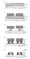
図1は、第一実施態様の回路基板の一例を示す概略平面図である。より具体的には、ハードディスクドライブ(HDD)に用いられるサスペンション用基板(フレキシャー)の一例を示す概略平面図である。なお、便宜上、カバー層の記載は省略している。図1に示される回路基板20は、一方の先端部分に形成された素子実装領域11と、他方の先端部分に形成された外部回路基板接続領域12と、素子実装領域11および外部回路基板接続領域12を電気的に接続する複数の配線層13a〜13dとを有するものである。配線層13aおよび配線層13bは一対の配線層であり、同様に、配線層13cおよび配線層13dも一対の配線層である。これらの2つの配線層は、一方がライト用の配線層であり、他方がリード用の配線層である。 FIG. 1 is a schematic plan view showing an example of a circuit board according to the first embodiment. More specifically, it is a schematic plan view showing an example of a suspension substrate (flexure) used in a hard disk drive (HDD). For convenience, the cover layer is not shown. A
図2(a)は、図1のA−A断面図である。図2(a)に示される回路基板は、金属支持基板1と、金属支持基板1上に形成された絶縁層2と、絶縁層2上に形成された配線層3とを有するものである。図2(b)は図2(a)の配線層3の拡大図であり、配線層3は、コアとなる第一配線部3aと、第一配線部3aの側面にめっき法により形成された第二配線部3bとを有する。また、第一実施態様の回路基板は、第一配線部3aおよび第二配線部3bの頂面の位置が一致していることを一つの特徴とする。 FIG. 2A is a cross-sectional view taken along the line AA in FIG. The circuit board shown in FIG. 2A has a metal supporting board 1, an insulating
第一実施態様によれば、第一配線部の側面に第二配線部が形成されていることから、配線間隔を狭くすることができ、配線層の微細化に適した回路基板とすることができる。この効果について図3を用いて説明する。第一実施態様の回路基板の配線層は、例えばサブトラクティブ法により形成することができる。従来のサブトラクティブ法では、図3(a)に示すように、レジストパターン6から露出する導体層(加工前の第一配線部3a)に対して、ウェットエッチング7を行う。この場合、配線間隔W1aはレジストパターン6の開口寸法に依存し、露光の描画安定性およびレジストの解像性には限界があることから、微細化は困難であった。これに対して、図3(b)に示すように、第一実施態様における配線層3は、第一配線部3aの側面に、めっき法により形成された第二配線部3bを有することから、従来のサブトラクティブ法の限界を超えて、配線間隔を狭くすることができる(W2a<W1a)。これにより、配線層の微細化を容易に図ることができる。さらに、第一実施態様によれば、第一配線部および第二配線部の頂面の位置が一致しているため、例えば配線層(端子)の上面に磁気ヘッド等の素子を実装する場合や、配線層(端子)とアンプとを金の超音波接合により接続する場合に、接合作業時のクリアランスを一定に保つことができ、良好な接触を実現できるという利点がある。According to the first embodiment, since the second wiring portion is formed on the side surface of the first wiring portion, the wiring interval can be reduced, and a circuit board suitable for miniaturization of the wiring layer can be obtained. it can. This effect will be described with reference to FIG. The wiring layer of the circuit board of the first embodiment can be formed by, for example, a subtractive method. In the conventional subtractive method, as shown in FIG. 3A, wet etching 7 is performed on the conductor layer (
また、第一実施態様の回路基板は、配線層の電気特性の向上を容易に図ることができるという利点もある。この効果について図4を用いて説明する。ここで、上述した図3(a)では、レジストパターン6の開口寸法をできるだけ小さくすることにより、配線間隔W1aを小さくしている。しかしながら、サブトラクティブ法では、厚さ方向のエッチングと同時に、幅方向のエッチング(サイドエッチング)が生じ、第一配線部3aの断面形状は台形状になる。さらに、第一配線部3aにおける頂面(上底)および底面(下底)の差が大きくなると(角度θ1aが小さくなると)、電気特性が低くなることが想定される。例えば、配線間の容量性結合が低下し、低インピーダンス化(特に高周波帯域での低インピーダンス化)を図ることが困難になる場合が想定される。In addition, the circuit board of the first embodiment has an advantage that the electrical characteristics of the wiring layer can be easily improved. This effect will be described with reference to FIG. Here, in FIG. 3A described above, the wiring interval W1a is reduced by making the opening size of the resist
これに対して、第一実施態様においては、図4(a)に示すように、配線間隔を狭くする目的に反して、敢えて第一配線部3aの配線間隔W1bを大きくすることができる。すなわち、従来よりもウェットエッチングを過剰に行うことにより、配線間隔W1bを大きくすることができる。これにより、第一配線部3aの断面形状を、台形状から矩形状に近づけることができる(角度θ1bを大きくすることができる)。その後、図4(b)に示すように、第一配線部3aの側面から、めっき法により第二配線部3bを成長させれば、めっきは等方的に成長するため、角度θ2bは角度θ1bと略同一となる。その結果、配線間隔W2bが小さく、かつ、電気特性が良好な配線層3とすることができる。ウェットエッチングを過剰に行うことにより角度θ1bが大きくなる理由は、レジストパターンに近い導体層の部分と、レジストパターンから遠い導体層の部分とでは、エッチングによる横方向の進み方が異なるからである。例えば、図5に示すように、レジストパターン6の露出部の下に存在する導体層3Xがウェットエッチングされるまでは、サイドエッチングの影響によりθは小さくなる。その後、ウェットエッチングを過剰に行うと、スプレー装置8から噴射されるエッチング液の影響を受けやすい絶縁層2に近い側の導体層3Xの部分では、エッチングの横方向の進み方が早く、エッチング液の影響を受けにくいレジストパターン6に近い側の導体層3Xの部分では、エッチングの横方向の進み方が遅くなる。その結果、θは大きくなる。エッチングの進み方は、スプレー圧、液の濃度、温度等によっても異なるが、定性的にはレジストの開口部中点を中心として放射線状に進む。On the other hand, in the first embodiment, as shown in FIG. 4A, contrary to the purpose of narrowing the wiring interval, the wiring interval W1b of the
一方、回路基板における配線層のパターニングの方法として、いわゆるアディティブ法が知られている。アディティブ法は、例えば図6に示すように、絶縁層2の表面にシード層(図示せず)を設け、その上にレジストパターン6を形成し、レジストパターン6から露出する表面に、めっき法により配線層3を形成する方法である。しかしながら、アディティブ法による配線形成には、以下のような欠点がある。まず、配線層3の形状および位置により、配線層3の高さが不均一になるという欠点がある。 On the other hand, a so-called additive method is known as a method for patterning a wiring layer on a circuit board. In the additive method, for example, as shown in FIG. 6, a seed layer (not shown) is provided on the surface of the insulating
配線層3の高さが不均一になる理由は、レジストパターンのサイズや配置に依存した電流密度の偏りが生じるからである。アディティブ法では、まず、配線層3を形成する位置に開口を有するレジストパターン6をフォトリソグラフィー等で形成する。次に、シード層(図示せず)を給電層として、配線層3を析出させる。この析出速度は電流密度に依存する。例えば、図6に示すように、細い配線層(領域I)と、太い配線層(パッド、領域III)とでは、細い配線層に電流が集中し、電流密度が高くなる。その結果、細い配線層における析出速度がより速くなる(A、B>D)。さらに、細い配線層であっても、3本もしくはそれ以上の細い配線層がほぼ等ピッチ間隔で配置された領域(領域I)と、1本もしくは2本程度の細い配線層が配置された領域(領域II)とでは、前者の方が電流が分散されるので、析出速度は後者の方が速くなる(C>A、B)。また、3本以上の複数の配線層がある場合(領域I)、最外の2本の配線層は、その内部の配線層よりも電流が集中するため、析出速度が速くなる(A、B)。このように、アディティブ法では、レジストパターンのサイズや配置に依存した電流密度の偏りが生じ、配線層の高さが不均一になりやすい。 The reason why the height of the
配線層の高さが不均一になることを防止するために、給電する電流値を下げたり、めっき液中において電極とワークとの間に、形状に合わせた遮蔽板を入れたりすることが考えられる。しかしながら、給電の電流値を下げることは、全体のめっき析出速度を下げることになり、生産性を著しく落とすことになる。さらに、遮蔽板も、レジストパターンに依存した析出速度の差を効果的に下げることは困難である。 In order to prevent the wiring layer height from becoming uneven, it may be possible to reduce the value of the current to be supplied or to insert a shielding plate that matches the shape between the electrode and the workpiece in the plating solution. It is done. However, lowering the current value of the power supply will lower the overall plating deposition rate, which will significantly reduce productivity. Furthermore, it is difficult for the shielding plate to effectively reduce the difference in deposition rate depending on the resist pattern.
また、配線層の高さが不均一であると、配線層(端子)の上面に磁気ヘッド等の素子を実装する場合や、配線層(端子)とアンプとを金の超音波接合により電気接続する場合に、接合作業時のクリアランスを一定に保てず、接触不良を起こす可能性がある。これに対して、第一実施態様においては、第一配線部および第二配線部の頂面の位置が一致しているため、このような問題は生じない。 Also, if the wiring layer height is not uniform, an element such as a magnetic head is mounted on the upper surface of the wiring layer (terminal), or the wiring layer (terminal) and the amplifier are electrically connected by gold ultrasonic bonding. In this case, the clearance during the joining operation cannot be kept constant, which may cause poor contact. On the other hand, in the first embodiment, such a problem does not occur because the positions of the top surfaces of the first wiring portion and the second wiring portion are the same.
また、アディティブ法による配線形成の他の欠点として、レジストパターン6を除去する際に、配線層3に割れや剥がれが生じやすくなるという欠点がある。アディティブ法では、図7(a)に示すように、レジストパターン6の開口部に配線層3を形成する。フォトリソグラフィーにより形成されたレジストパターン6の断面形状は、通常、矩形ではなく台形になる。そのため、レジストパターン6の開口部で析出した配線層3の断面形状は、逆台形になる。その結果、レジストパターン6を除去する際に、レジストパターン6が膨潤すると、レジストパターン6が抜けにくくなってしまう。さらに、膨潤する力が強ければ、配線層3に対して横の力が働く。そのため、配線層3に割れや剥がれが生じやすくなる。また、配線層3の断面形状が逆台形であるため、配線層3と絶縁層2との密着性が、サブトラクティブ法の場合に比べて低くなる。さらに、密着性の低下という観点では、レジストパターン6を除去した後にシード層9を除去する場合(図7(b))、シード層9が過剰に除去されるアンダーカットが生じやすく(図7(c))、配線層3と絶縁層2との密着性が、さらに低くなることが想定される。これに対して、第一実施態様においては、例えばサブトラクティブ法により第一配線部3を形成できるため、上記のような欠点は生じない。 Further, as another defect of the wiring formation by the additive method, there is a defect that when the resist
第一実施態様の回路基板は、少なくとも絶縁層および配線層を有するものである。さらに、配線層が形成された側とは反対側の絶縁層の表面に、金属支持基板が配置されていても良い。また、配線層を覆うカバー層が形成されていても良い。
以下、第一実施態様の回路基板について、構成ごとに説明する。The circuit board of the first embodiment has at least an insulating layer and a wiring layer. Furthermore, a metal supporting board may be disposed on the surface of the insulating layer opposite to the side on which the wiring layer is formed. Further, a cover layer covering the wiring layer may be formed.
Hereinafter, the circuit board of the first embodiment will be described for each configuration.
(1)配線層
第一実施態様における配線層は、後述する絶縁層上に形成されるものである。また、第一実施態様における配線層が、第一配線部と、第一配線部の側面にめっき法により形成された第二配線部とを有する。さらに、第一実施態様においては、第一配線部および第二配線部の頂面の位置が一致している。(1) Wiring layer The wiring layer in a 1st embodiment is formed on the insulating layer mentioned later. Moreover, the wiring layer in the first embodiment includes a first wiring portion and a second wiring portion formed on the side surface of the first wiring portion by a plating method. Furthermore, in the first embodiment, the positions of the top surfaces of the first wiring portion and the second wiring portion are the same.
第一配線部の材料は、導電性を有するものであれば特に限定されるものではないが、例えば金属を挙げることができる。具体的には、銅(Cu)、銅合金等を挙げることができ、中でも銅(Cu)が好ましい。導電性に優れ、安価だからである。また、銅合金としては、例えば、銅(Cu)と、亜鉛(Zn)、クロム(Cr)、スズ(Sn)およびケイ素(Si)からなる群から選択される少なくとも一種以上の元素との合金を挙げることができる。また、第一配線部の断面形状としては、例えば台形状および矩形状を挙げることができる。 The material of the first wiring part is not particularly limited as long as it has conductivity, and examples thereof include metals. Specifically, copper (Cu), a copper alloy, etc. can be mentioned, and copper (Cu) is particularly preferable. This is because it is highly conductive and inexpensive. As the copper alloy, for example, an alloy of copper (Cu) and at least one element selected from the group consisting of zinc (Zn), chromium (Cr), tin (Sn), and silicon (Si) is used. Can be mentioned. In addition, examples of the cross-sectional shape of the first wiring portion include a trapezoidal shape and a rectangular shape.
一方、第二配線部の材料は、導電性を有し、めっき法(電解めっき法、無電解めっき法)により形成可能なものであれば特に限定されるものではなく、通常は金属である。具体的には、銅(Cu)、ニッケル(Ni)、銀(Ag)、金(Au)、パラジウム(Pd)、スズ(Sn)、および、これらの金属を一種または二種以上含有する合金等を挙げることができ、中でも、銅(Cu)、ニッケル(Ni)、銀(Ag)、金(Au)、パラジウム(Pd)、および、これらの金属を一種または二種以上含有する合金であることが好ましい。また、第二配線部は、単層構造であっても良く、二層以上の積層構造であっても良い。ここで、第二配線部がNiめっき部を有していれば、機械的強度の向上を図ることができる。また、第二配線部がAgめっき部、Auめっき部のような貴金属めっき部を有していれば、耐腐食性に優れた配線層とすることができる。貴金属めっき部は第二配線部の最も外側に形成されていることが好ましい。また、特に第一実施態様においては、第二配線部がCuめっき部から構成されるもの、第二配線部が内側からCuめっき部およびNiめっき部を有するもの、第二配線部が内側からCuめっき部、Niめっき部およびAuめっき部を有するもののいずれかであることが好ましい。 On the other hand, the material of the second wiring portion is not particularly limited as long as it has conductivity and can be formed by a plating method (electrolytic plating method, electroless plating method), and is usually a metal. Specifically, copper (Cu), nickel (Ni), silver (Ag), gold (Au), palladium (Pd), tin (Sn), an alloy containing one or more of these metals, and the like Among them, copper (Cu), nickel (Ni), silver (Ag), gold (Au), palladium (Pd), and an alloy containing one or more of these metals. Is preferred. Further, the second wiring portion may have a single layer structure or a laminated structure of two or more layers. Here, if the second wiring part has the Ni plating part, the mechanical strength can be improved. Moreover, if the 2nd wiring part has noble metal plating parts like Ag plating part and Au plating part, it can be set as the wiring layer excellent in corrosion resistance. The noble metal plating part is preferably formed on the outermost side of the second wiring part. In particular, in the first embodiment, the second wiring part is composed of a Cu plating part, the second wiring part has a Cu plating part and a Ni plating part from the inside, and the second wiring part is Cu from the inside. It is preferably any one having a plating part, a Ni plating part and an Au plating part.
第一配線部の側面に第二配線部が形成されているか否かは、例えば、走査型電子顕微鏡(SEM)観察、透過型電子顕微鏡(TEM)観察、X線光電子分光(XPS)分析、蛍光X線(XRF)分析等により確認できる。なお、第一配線部および第二配線部の材料が同じである場合であっても、第一配線部の結晶粒径と、第二配線部の結晶粒径とが全く同じになることは通常起こり得ないことから、第一配線部および第二配線部の間には界面が形成され、この界面の存在を確認することで、第一配線部の側面に第二配線部が形成されていることを確認できる。 Whether or not the second wiring part is formed on the side surface of the first wiring part is determined by, for example, scanning electron microscope (SEM) observation, transmission electron microscope (TEM) observation, X-ray photoelectron spectroscopy (XPS) analysis, fluorescence It can be confirmed by X-ray (XRF) analysis or the like. Even if the materials of the first wiring part and the second wiring part are the same, the crystal grain size of the first wiring part and the crystal grain size of the second wiring part are usually the same. Since this cannot occur, an interface is formed between the first wiring part and the second wiring part, and the second wiring part is formed on the side surface of the first wiring part by confirming the existence of this interface. I can confirm that.
上述したように、第一配線部をサブトラクティブ法により形成する場合、通常は、第一配線部の断面形状が台形状になる。ここで、図8に示すように、第一配線部3aの底面の幅をWaとし、第一配線部3aの頂面の幅をWbとし、第二配線部3bの幅をWcとし、配線層3の厚さをWdとし、隣り合う配線層3の配線間隔をW2とする。Waの値は、例えば20μm以下であることが好ましく、18μm以下であることがより好ましい。Waの値が大きすぎると、目的とする微細構造を得ることができない可能性があるからである。一方、Waの値は、例えば10μm以上であることが好ましく、12μm以上であることがより好ましい。Waの値が小さすぎると、第一配線部3aと絶縁層2との密着性が低くなる可能性があるからである。As described above, when the first wiring portion is formed by the subtractive method, the cross-sectional shape of the first wiring portion is usually trapezoidal. Here, as shown in FIG. 8, the width of the bottom surface of the
Wbの値は、例えば5μm〜15μmの範囲内であることが好ましく、7μm〜10μmの範囲内であることがより好ましい。Wbの値が大きすぎると、目的とする微細構造を得ることができない可能性があるからであり、Wbの値が小さすぎると、レジストパターンを保持できず、レジストに割れが生じる可能性があるからである。さらに、第一配線部3における底面の長さと頂面の長さとの差(Wa−Wb)は、例えば15μm以下であることが好ましく、10μm以下であることがより好ましく、5μm以下であることがさらに好ましい。また、第二配線部は、めっき法により等方的に形成されたものであることから、通常、θ1とθ2とは一致する。θ1およびθ2は、それぞれ、58°〜90°の範囲内であることが好ましく、63°〜80°の範囲内であることがより好ましい。例えば、第一配線層の厚さが12μmであり、かつ、台形の片側の張り出し部分の長さが7.5μmである場合、その角度は58°になる(arctan(12/7.5))。同様に、台形の片側の張り出し部分の長さが5μmである場合、その角度は63°になり(arctan(12/5))、台形の片側の張り出し部分の長さが2μmである場合、その角度は80°になる。The value of Wb is preferably in the range of 5 μm to 15 μm, for example, and more preferably in the range of 7 μm to 10 μm. When the value of Wb is too large, it is a possibility that it is impossible to obtain a fine structure of interest, the value of Wb is too small, it can not hold a resist pattern, a possibility that cracking occurs in the resist Because there is. Furthermore, the difference (Wa −Wb ) between the length of the bottom surface and the length of the top surface in the
Wcの値は、例えば0.5μm〜10μmの範囲内であることが好ましく、0.5μm〜5μmの範囲内であることがより好ましい。また、Wc/Waの値は、例えば0.03以上であり、0.03〜1.0の範囲内であることが好ましく、0.03〜0.5の範囲内であることがより好ましく、0.03〜0.1の範囲内であることがさらに好ましく、0.03〜0.05の範囲内であることが特に好ましい。また、Wdの値は、例えば3μm〜25μmの範囲内であることが好ましく、5μm〜12μmの範囲内であることがより好ましい。また、W2の値は、配線層のパターンによって大きく異なるものであるが、隣り合う配線層が最も近接した位置でのW2の値は、例えば5μm〜25μmの範囲内であることが好ましく、5μm〜20μmの範囲内であることがより好ましく、5μm〜10μmの範囲内であることがさらに好ましい。W2の値が大きすぎると、目的とする微細構造を得ることができない可能性があり、W2の値が小さすぎると、短絡が生じる可能性があるからである。The value of Wc is preferably in the range of 0.5 μm to 10 μm, for example, and more preferably in the range of 0.5 μm to 5 μm. In addition, the value of Wc / Wa is, for example, 0.03 or more, preferably in the range of 0.03 to 1.0, and more preferably in the range of 0.03 to 0.5. Preferably, it is in the range of 0.03-0.1, more preferably in the range of 0.03-0.05. Further, the value of Wd is preferably in the range of 3 μm to 25 μm, for example, and more preferably in the range of 5 μm to 12 μm. Further, the value of W2 varies greatly depending on the pattern of the wiring layer, but the value of W2 at the position where the adjacent wiring layers are closest to each other is preferably in the range of 5 μm to 25 μm, for example. It is more preferably in the range of 5 μm to 20 μm, and still more preferably in the range of 5 μm to 10 μm. This is because if the value of W2 is too large, the target microstructure may not be obtained, and if the value of W2 is too small, a short circuit may occur.
また、図9(a)に示すように、配線層3はカバー層4により覆われていても良い。配線層の劣化(例えば腐食)を防止できるからである。カバー層の材料としては、例えば、上述した絶縁層の材料として記載した樹脂を挙げることができ、中でもポリイミド樹脂が好ましい。また、カバー層の材料は、感光性材料であっても良く、非感光性材料であっても良い。カバー層の厚さは、例えば2μm〜30μmの範囲内であることが好ましく、2μm〜10μmの範囲内であることがより好ましい。 Further, as shown in FIG. 9A, the
また、図9(b)、(c)に示すように、配線層3の表面には、保護めっき部5が形成されていても良い。保護めっき部を設けることにより、配線層の劣化(腐食等)を防止できるからである。保護めっき部の種類は特に限定されるものではないが、例えばNiめっき、Auめっき等を挙げることができる。保護めっき部の厚さは、例えば0.1μm〜4.0μmの範囲内である。また、第一実施態様においては、素子または外部回路基板との電気的な接続を行う端子部に保護めっき部が形成されていることが好ましい。なお、図9(c)に示すように、絶縁層2が存在しないフライングリード部に、第二配線部3bが形成されることで、フライングリード部の機械的強度が向上するという利点がある。フライングリード部は、図10に示すように、配線層3が、金属支持基板(図示せず)、絶縁層2およびカバー層4等から露出した部分をいう。例えば、第一実施態様の回路基板がサスペンション用基板である場合、磁気ヘッド等の素子からピックアップした信号をアンプにつなげるための接続端子領域に、フライングリード構造を採用することができる。なお、図9(c)は、図10のA−A断面図に相当する。 Further, as shown in FIGS. 9B and 9C, a
第一実施態様においては、第一配線部の側面に第二配線部が形成されていることを一つの特徴としているが、第二配線部は、第一配線部の全長に渡って形成されている必要はなく、第一配線部の少なくとも一部に形成されていれば良い。例えば、第二配線部は、素子との電気的な接続を行う端子部のみに形成されたものであっても良く、外部回路基板との電気的な接続を行う端子部のみに形成されたものであっても良く、第一配線部の全長に渡って形成されたものであっても良い。 The first embodiment is characterized in that the second wiring portion is formed on the side surface of the first wiring portion, but the second wiring portion is formed over the entire length of the first wiring portion. It is not necessary to be formed on at least a part of the first wiring portion. For example, the second wiring portion may be formed only in the terminal portion that performs electrical connection with the element, or may be formed only in the terminal portion that performs electrical connection with the external circuit board. It may be formed over the entire length of the first wiring portion.
また、第一実施態様における配線層の機能は、特に限定されるものではなく、回路基板の種類に応じて適宜選択されるものである。例えば回路基板がサスペンション用基板である場合、配線層の種類は、例えばライト配線層、リード配線層、ノイズシールド用配線層、クロストーク防止用配線層、電源用配線層、グランド用配線層、フライトハイトコントロール用配線層、センサー用配線層、アクチュエータ用配線層、熱アシスト用配線層等を挙げることができる。 Moreover, the function of the wiring layer in the first embodiment is not particularly limited, and is appropriately selected according to the type of the circuit board. For example, when the circuit board is a suspension board, the types of wiring layers include, for example, a write wiring layer, a lead wiring layer, a noise shield wiring layer, a crosstalk prevention wiring layer, a power wiring layer, a ground wiring layer, and a flight. Examples thereof include a height control wiring layer, a sensor wiring layer, an actuator wiring layer, and a heat assist wiring layer.
(2)絶縁層
第一実施態様における絶縁層は、配線層を他の部材から絶縁する層である。絶縁層の材料は、絶縁性を有するものであれば特に限定されるものではないが、例えば樹脂を挙げることができる。上記樹脂としては、例えばポリイミド樹脂、ポリベンゾオキサゾール樹脂、ポリベンゾイミダゾール樹脂、アクリル樹脂、ポリエーテルニトリル樹脂、ポリエーテルスルホン樹脂、ポリエチレンテレフタレート樹脂、ポリエチレンナフタレート樹脂およびポリ塩化ビニル樹脂を挙げることができ、中でもポリイミド樹脂が好ましい。絶縁性、耐熱性および耐薬品性に優れているからである。また、絶縁層の材料は、感光性材料であっても良く、非感光性材料であっても良い。(2) Insulating layer The insulating layer in the first embodiment is a layer that insulates the wiring layer from other members. The material of the insulating layer is not particularly limited as long as it has insulating properties, and examples thereof include a resin. Examples of the resin include polyimide resin, polybenzoxazole resin, polybenzimidazole resin, acrylic resin, polyether nitrile resin, polyether sulfone resin, polyethylene terephthalate resin, polyethylene naphthalate resin, and polyvinyl chloride resin. Of these, polyimide resin is preferred. It is because it is excellent in insulation, heat resistance and chemical resistance. In addition, the material of the insulating layer may be a photosensitive material or a non-photosensitive material.
絶縁層の厚さは、回路基板の種類に応じて異なるものであり、特に限定されるものではない。例えば、回路基板がサスペンション用基板である場合、絶縁層の厚さは、例えば5μm〜30μmの範囲内であることが好ましく、5μm〜18μmの範囲内であることがより好ましく、5μm〜12μmの範囲内であることがさらに好ましい。 The thickness of the insulating layer varies depending on the type of circuit board and is not particularly limited. For example, when the circuit board is a suspension board, the thickness of the insulating layer is, for example, preferably in the range of 5 μm to 30 μm, more preferably in the range of 5 μm to 18 μm, and in the range of 5 μm to 12 μm. More preferably, it is within.
(3)金属支持基板
第一実施態様の回路基板は、配線層が形成された側とは反対側の絶縁層の表面に、金属支持基板を有することが好ましい。例えばサスペンション用基板として有用な回路基板とすることができるからである。金属支持基板の材料は、回路基板の種類に応じて異なるものであり、特に限定されるものではない。例えば回路基板がサスペンション用基板である場合、金属支持基板の材料は、ばね性を有する金属であることが好ましく、SUSであることがより好ましい。また、金属支持基板の厚さは、回路基板の種類に応じて異なるものであるが、例えば10μm〜20μmの範囲内である。(3) Metal Support Board The circuit board of the first embodiment preferably has a metal support board on the surface of the insulating layer opposite to the side on which the wiring layer is formed. This is because, for example, a circuit board useful as a suspension board can be obtained. The material of the metal supporting board varies depending on the type of circuit board and is not particularly limited. For example, when the circuit board is a suspension board, the material of the metal support board is preferably a spring metal, and more preferably SUS. Moreover, although the thickness of a metal support substrate changes with kinds of circuit board, it exists in the range of 10 micrometers-20 micrometers, for example.
(4)回路基板
第一実施態様の回路基板は、上述した配線層および絶縁層を有するものであれば特に限定されるものではない。回路基板の用途としては、例えば、HDD用回路基板を挙げることができる。HDD用回路基板としては、例えばサスペンション用基板(フレキシャー)および中継基板等を挙げることができる。また、第一実施態様の回路基板は、一般的なプリント基板(PC)およびフレキシブルプリント基板(FPC)に用いることができる。(4) Circuit board The circuit board of the first embodiment is not particularly limited as long as it has the wiring layer and the insulating layer described above. As an application of the circuit board, for example, a circuit board for HDD can be cited. Examples of HDD circuit boards include suspension boards (flexures) and relay boards. The circuit board of the first embodiment can be used for a general printed circuit board (PC) and a flexible printed circuit board (FPC).
2.第二実施態様
次に、本発明の回路基板の第二実施態様について説明する。第二実施態様の回路基板は、絶縁層と、上記絶縁層上に形成された配線層とを有する回路基板であって、上記配線層が、第一配線部と、上記第一配線部の側面および頂面にめっき法により形成され、上記第一配線部と同一材料の第三配線部とを有することを特徴とするものである。2. Second Embodiment Next, a second embodiment of the circuit board of the present invention will be described. The circuit board of the second embodiment is a circuit board having an insulating layer and a wiring layer formed on the insulating layer, wherein the wiring layer includes a first wiring part and a side surface of the first wiring part. Further, the first wiring part is formed on the top surface by a plating method and has a third wiring part made of the same material as the first wiring part.
図11(a)は、図2(a)と同様に図1のA−A断面図に相当するものである。図11(a)に示される回路基板は、金属支持基板1と、金属支持基板1上に形成された絶縁層2と、絶縁層2上に形成された配線層3とを有するものである。図11(b)は図11(a)の配線層3の拡大図であり、配線層3は、コアとなる第一配線部3aと、第一配線部3aの側面および頂面にめっき法により形成され、第一配線部3aと同一材料の第三配線部3cとを有する。 FIG. 11A corresponds to the AA cross-sectional view of FIG. 1 like FIG. 2A. The circuit board shown in FIG. 11A has a metal supporting board 1, an insulating
第二実施態様によれば、第一配線部の側面および頂面に、第三配線部が形成されていることから、配線間隔を狭くすることができ、配線層の微細化に適した回路基板とすることができる。なお、第二実施態様の回路基板は、第一配線部の側面および頂面に第三配線部が形成されていること以外は、第一実施態様の回路基板と同様であるので、ここでの記載は省略する。 According to the second embodiment, since the third wiring portion is formed on the side surface and the top surface of the first wiring portion, the wiring interval can be reduced, and the circuit board suitable for miniaturization of the wiring layer. It can be. The circuit board of the second embodiment is the same as the circuit board of the first embodiment except that the third wiring part is formed on the side surface and the top surface of the first wiring part. Description is omitted.
B.回路基板の製造方法
次に、本発明の回路基板の製造方法について説明する。本発明の回路基板の製造方法は、配線層の構成により、2つの実施態様に大別することができる。B. Next, a method for manufacturing a circuit board according to the present invention will be described. The method for manufacturing a circuit board according to the present invention can be roughly divided into two embodiments according to the configuration of the wiring layer.
1.第一実施態様
本発明の回路基板の製造方法の第一実施態様は、絶縁層と、上記絶縁層上に形成された配線層とを有する回路基板の製造方法であって、上記配線層を形成するための導体層の表面にレジストパターンを形成し、上記レジストパターンから露出する上記導体層を、上記レジストパターンの裏面が露出するようにウェットエッチングし、第一配線部を形成する第一配線部形成工程と、上記レジストパターンを残した状態で、上記第一配線部の側面に、めっき法により第二配線部を形成する第二配線部形成工程と、を有することを特徴とするものである。1. 1st embodiment The 1st embodiment of the manufacturing method of the circuit board of this invention is a manufacturing method of the circuit board which has an insulating layer and the wiring layer formed on the said insulating layer, Comprising: Forming the said wiring layer Forming a first wiring part by forming a resist pattern on the surface of the conductive layer to be etched, wet etching the conductive layer exposed from the resist pattern so that the back surface of the resist pattern is exposed, and forming a first wiring part; And a second wiring portion forming step of forming a second wiring portion by plating on the side surface of the first wiring portion with the resist pattern remaining. .
図12は、第一実施態様の回路基板の製造方法の一例を示す概略断面図である。図12においては、まず、絶縁層2と導体層3Xとを有する積層部材を準備する(図12(a))。次に、導体層3Xの表面にドライフィルムレジスト(DFR)をラミネートし、露光、現像を行うことにより、レジストパターン6を形成する(図12(b))。次に、レジストパターンから露出する導体層6をウェットエッチングし、第一配線部3aを形成する(図12(c))。この際、深さ方向において絶縁層2が露出し、かつ、幅方向においてレジストパターン6の裏面が露出するようにウェットエッチングを行う。その後、レジストパターン6を残した状態で、第一配線部3aの側面に、めっき法により第二配線部3bを形成する(図12(d))。最後に、レジストパターン6を除去して、回路基板20を得る(図12(e))。 FIG. 12 is a schematic cross-sectional view showing an example of a method for manufacturing a circuit board according to the first embodiment. In FIG. 12, first, a laminated member having the insulating
第一実施態様によれば、第一配線部を形成し、その後のめっき法により第二配線部を形成することで、配線間隔を狭くすることができ、配線層の微細化に適した回路基板を得ることができる。また、レジストパターンを残した状態で第二配線部を形成することにより、第一配線部および第二配線部の頂面の位置が一致した回路基板を得ることができる。また、レジストパターンの裏面には、存在していた導体層の凹凸が転写されていることから、めっきの種類(光沢、無光沢)によらず、エッチングされた導体層の表面を第二配線部で再現することができる。
以下、第一実施態様の回路基板の製造方法について、工程ごとに説明する。According to the first embodiment, the first wiring portion is formed, and the second wiring portion is formed by a subsequent plating method, whereby the wiring interval can be narrowed, and the circuit board suitable for miniaturization of the wiring layer Can be obtained. Further, by forming the second wiring portion with the resist pattern remaining, a circuit board in which the positions of the top surfaces of the first wiring portion and the second wiring portion are matched can be obtained. In addition, since the unevenness of the existing conductor layer is transferred to the back surface of the resist pattern, the surface of the etched conductor layer can be used as the second wiring portion regardless of the type of plating (glossy or matte). Can be reproduced.
Hereinafter, the manufacturing method of the circuit board of the first embodiment will be described for each process.
(1)第一配線部形成工程
第一実施態様における第一配線部形成工程は、上記配線層を形成するための導体層の表面にレジストパターンを形成し、上記レジストパターンから露出する上記導体層を、上記レジストパターンの裏面が露出するようにウェットエッチングし、第一配線部を形成する工程である。(1) First Wiring Portion Forming Step The first wiring portion forming step in the first embodiment includes forming a resist pattern on the surface of the conductor layer for forming the wiring layer and exposing the conductor layer from the resist pattern. Is a step of performing wet etching so that the back surface of the resist pattern is exposed to form a first wiring portion.
第一実施態様における絶縁層および導体層については、上述した「A.回路基板」に記載した内容と同様である。また、導体層は、めっき法(電解めっき法、無電解めっき法)により形成されたものであっても良く、金属箔を絶縁層に張り合わせて形成されたものであっても良い。 The insulating layer and the conductor layer in the first embodiment are the same as those described in “A. Circuit board”. The conductor layer may be formed by a plating method (electrolytic plating method, electroless plating method), or may be formed by bonding a metal foil to an insulating layer.
第一実施態様に用いられるレジストは、エッチング液に対する耐性を有するものであれば特に限定されるものではないが、通常、感光性レジストである。さらに、感光性レジストとしては、具体的には、アクリル系レジスト、ノボラック系レジスト等を挙げることができる。また、上記レジストは、ドライフィルムレジストであっても良く、液状レジストであっても良い。なお、後述する第二配線部形成工程でシアン浴を用いる場合は、耐薬品性に優れたレジストを用いることが好ましい。 The resist used in the first embodiment is not particularly limited as long as it has resistance to an etching solution, but is usually a photosensitive resist. Furthermore, specific examples of the photosensitive resist include acrylic resists and novolac resists. The resist may be a dry film resist or a liquid resist. In addition, when using a cyan bath in the 2nd wiring part formation process mentioned later, it is preferable to use the resist excellent in chemical resistance.
ウェットエッチングに用いられるエッチング液は、導体層の材料に応じて異なるものであるが、例えば導体層の材料が銅である場合、エッチング液として、塩化鉄系エッチング液を用いることができる。 The etching solution used for the wet etching varies depending on the material of the conductor layer. For example, when the material of the conductor layer is copper, an iron chloride-based etching solution can be used as the etching solution.
また、第一実施態様においては、導体層に対して、レジストパターンの裏面が露出するようにウェットエッチングする。これにより、図12(d)に示したように、レジストパターン6の裏面の露出部分に沿って、第二配線部3bが形成される。さらに、第一実施態様においては、図4(a)に示したように、第一配線部3aにおける底面および側面のなす角度θ1bが大きくなるようにエッチングを行うことが好ましい。電気特性が良好な配線層を得ることができるからである。なお、好ましい角度およびその他の寸法については、上述した図8で説明した内容と同様であるので、ここでの記載は省略する。In the first embodiment, the conductor layer is wet-etched so that the back surface of the resist pattern is exposed. As a result, as shown in FIG. 12D, the
また、図13に示すように、レジストパターン6の裏面の露出部分の幅をW3とし、隣り合う第一配線部3aの配線間隔をW1とした場合、W1およびW3は、W1>W3×2を満たすことが好ましい。第二配線部の幅を最大限に大きくしても、短絡が生じないからである。なお、短絡防止の観点からは、W1>W3×2.5を満たすことがより好ましく、W1>W3×3を満たすことがさらに好ましい。Further, as shown in FIG. 13, if the width of the rear surface exposed portion of the resist
また、本発明における「過剰なウェットエッチング」は、例えば、目的とする設計寸法よりも過剰にウェットエッチングすること、と定義することもできる。例えば、目的とする所定のL/S(ラインアンドスペース)に対してラインの寸法を意図的に小さくした場合は、過剰なウェットエッチングに該当する。具体的には、L/S=20/20(μm)を目的とする場合は、Lを20μmよりも小さくすること(例えばL/S=15/25(μm))が、過剰なウェットエッチングに該当する。なお、L/Sは、通常、底辺の間隔で検討されるものであることから、ラインの断面形状によらず評価することができる。 In addition, “excess wet etching” in the present invention can be defined as, for example, excessive wet etching beyond a target design dimension. For example, when the line size is intentionally reduced with respect to a predetermined predetermined L / S (line and space), it corresponds to excessive wet etching. Specifically, when L / S = 20/20 (μm) is aimed, L is made smaller than 20 μm (for example, L / S = 15/25 (μm)) for excessive wet etching. Applicable. In addition, since L / S is normally considered by the space | interval of a base, it can be evaluated irrespective of the cross-sectional shape of a line.
また、図14は、ウェットエッチング時の第一配線部の底部の形状を示す概略平面図である。図14(a)に示すように、ウェットエッチングの初期の段階では、第一配線部3aの底部形状の直線性が悪い。その後、ある程度エッチングが進むと、図14(b)に示すように、レジストパターン(図示せず)の形状に対応して、第一配線部3aの底部形状の直線性が良くなる。このように、第一実施態様においては、第一配線部3aの底部の形状が、レジストパターンに対応する形状になるまで、ウェットエッチングを行うことが好ましい。 FIG. 14 is a schematic plan view showing the shape of the bottom of the first wiring part during wet etching. As shown in FIG. 14A, at the initial stage of wet etching, the linearity of the bottom shape of the
(2)第二配線部形成工程
第一実施態様における第二配線部形成工程は、上記レジストパターンを残した状態で、上記第一配線部の側面に、めっき法により第二配線部を形成する工程である。(2) Second wiring portion forming step In the second wiring portion forming step in the first embodiment, the second wiring portion is formed by plating on the side surface of the first wiring portion with the resist pattern remaining. It is a process.
第二配線部を形成するめっき法は、電解めっき法であっても良く、無電解めっき法であっても良いが、電解めっき法が好ましい。電解ニッケルめっきとしては、例えばワット浴ニッケルめっき、ジュールニッケルめっき、サチライトニッケルめっき、スルファミン酸浴ニッケルめっき、ウッド浴ニッケルストライクめっき等を挙げることができる。また、電解金めっきとしては、例えばシアン浴金めっき、酸性浴金めっき等を挙げることができる。また、電解銅めっきとしては、例えば硫酸浴銅めっき、ピロリン酸浴銅めっき、シアン浴銅めっき等を挙げることができる。なお、本工程においては、めっき法を2回以上繰り返すことによって、積層構造を有する第二配線部を形成することができる。 The plating method for forming the second wiring portion may be an electrolytic plating method or an electroless plating method, but an electrolytic plating method is preferred. Examples of the electrolytic nickel plating include Watt bath nickel plating, Joule nickel plating, satellite nickel plating, sulfamic acid bath nickel plating, and wood bath nickel strike plating. Examples of the electrolytic gold plating include cyan bath gold plating and acid bath gold plating. Examples of the electrolytic copper plating include sulfuric acid bath copper plating, pyrophosphate bath copper plating, and cyan bath copper plating. In this step, the second wiring part having a laminated structure can be formed by repeating the plating method twice or more.
第一実施態様においては、上述した第一配線部形成工程および第二配線形成部により、回路基板を得ることができる。ここで、回路基板がサスペンション用基板である場合について、その具体的な製造方法を、図15を用いて説明する。図15においては、まず、金属支持部材1X、絶縁部材2Xおよび導体層(導体部材)3Xをこの順に有する積層部材を準備する(図15(a))。次に、導体部材3Xの表面上に、DFRをラミネートし、露光および現像を行うことにより、レジストパターン6を形成する(図15(b))。この際、金属支持部材1Xの表面に同様のレジストパターンを形成し、治具孔等を同時に形成しても良い。次に、レジストパターン6から露出する導体部材3Xをウェットエッチングし、第一配線部3aを形成する(図15(c))。次に、レジストパターン6を残した状態で、第一配線部3aの側面に、めっき法により第二配線部3bを形成し(図15(d))、次いでレジストパターン6を除去する(図15(e))。その後、配線層3を覆うカバー層4を形成する(図15(f))。次に、図示しない箇所の絶縁部材2Xをウェットエッチングし、絶縁層2を形成する。次に、同じく図示しない箇所の金属支持部材1Xをウェットエッチングすることで、外形加工を行い、金属支持基板1を形成する。これにより、サスペンション用基板を得る(図15(g))。 In the first embodiment, a circuit board can be obtained by the first wiring portion forming step and the second wiring forming portion described above. Here, when the circuit board is a suspension board, a specific manufacturing method will be described with reference to FIG. In FIG. 15, first, a laminated member having a
また、図15においては、種々のウェットエッチングを行っているが、ウェットエッチングに用いられるエッチング液は、各材料の特性を考慮して、適宜選択することが好ましい。例えば、金属支持基板にSUSを用いている場合、および、配線層に銅を用いている場合には、エッチング液として、例えば塩化鉄系エッチング液を用いることができる。また、絶縁層およびカバー層にポリイミド樹脂を用いている場合は、エッチング液として、例えばアルカリ系エッチング液(例えば有機アミン化合物および水酸化ナトリウムを含むエッチング液)を用いることができる。 In FIG. 15, various wet etching is performed, but it is preferable that an etching solution used for the wet etching is appropriately selected in consideration of characteristics of each material. For example, when SUS is used for the metal support substrate and copper is used for the wiring layer, for example, an iron chloride-based etchant can be used as the etchant. In the case where a polyimide resin is used for the insulating layer and the cover layer, for example, an alkaline etching solution (for example, an etching solution containing an organic amine compound and sodium hydroxide) can be used as the etching solution.
2.第二実施態様
次に、本発明の回路基板の製造方法の第二実施態様について説明する。第二実施態様の回路基板の製造方法は、絶縁層と、上記絶縁層上に形成された配線層とを有する回路基板の製造方法であって、上記配線層を形成するための導体層の表面にレジストパターンを形成し、上記レジストパターンから露出する上記導体層を、上記レジストパターンの裏面が露出するようにウェットエッチングし、第一配線部を形成する第一配線部形成工程と、上記レジストパターンを除去した状態で、上記第一配線部の側面および頂面に、めっき法により、上記第一配線部と同一材料の第三配線部を形成する第三配線部形成工程と、を有することを特徴とするものである。2. Second Embodiment Next, a second embodiment of the circuit board manufacturing method of the present invention will be described. A method for manufacturing a circuit board according to a second embodiment is a method for manufacturing a circuit board having an insulating layer and a wiring layer formed on the insulating layer, and the surface of the conductor layer for forming the wiring layer Forming a first resist pattern, and wet-etching the conductive layer exposed from the resist pattern so that the back surface of the resist pattern is exposed to form a first wiring portion; and the resist pattern A third wiring part forming step of forming a third wiring part of the same material as that of the first wiring part on a side surface and a top surface of the first wiring part by a plating method. It is a feature.
第二実施態様によれば、第一配線部を形成し、その後のめっき法により第三配線部を形成することで、配線間隔を狭くすることができ、配線層の微細化に適した回路基板を得ることができる。なお、第二実施態様の回路基板の製造方法は、レジストパターンを除去した状態で第三配線部を形成すること以外は、第一実施態様の回路基板の製造方法と同様であるので、ここでの記載は省略する。 According to the second embodiment, the first wiring portion is formed, and then the third wiring portion is formed by a subsequent plating method, whereby the wiring interval can be narrowed, and the circuit board suitable for miniaturization of the wiring layer Can be obtained. The method for manufacturing the circuit board according to the second embodiment is the same as the method for manufacturing the circuit board according to the first embodiment except that the third wiring portion is formed with the resist pattern removed. Is omitted.
C.サスペンション用基板
次に、本発明のサスペンション用基板について説明する。本発明のサスペンション用基板は、上述した回路基板であることを特徴とするものである。なお、サスペンション用基板は、通常、配線層が形成された側とは反対側の絶縁層の表面に、金属支持基板が配置されたものである。C. Next, the suspension substrate of the present invention will be described. The suspension board of the present invention is the circuit board described above. The suspension substrate is usually a metal support substrate disposed on the surface of the insulating layer opposite to the side on which the wiring layer is formed.
本発明によれば、上述した回路基板を用いることで、配線層の微細化に適したサスペンション用基板とすることができる。なお、サスペンション用基板の具体例については、上述した図1、図2、図11で説明した内容と同様であるので、ここでの記載は省略する。 According to the present invention, by using the circuit board described above, a suspension board suitable for miniaturization of the wiring layer can be obtained. A specific example of the suspension substrate is the same as that described with reference to FIGS. 1, 2, and 11, and is not described here.
D.サスペンション
次に、本発明のサスペンションについて説明する。本発明のサスペンションは、上述したサスペンション用基板を含むことを特徴とするものである。D. Suspension Next, the suspension of the present invention will be described. The suspension of the present invention includes the above-described suspension substrate.
本発明によれば、上述したサスペンション用基板を用いることで、配線層の微細化に適したサスペンションとすることができる。 According to the present invention, a suspension suitable for miniaturization of the wiring layer can be obtained by using the suspension substrate described above.
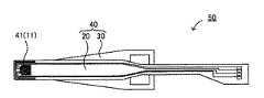
図16は、本発明のサスペンションの一例を示す概略平面図である。図16に示されるサスペンション40は、上述したサスペンション用基板20と、素子実装領域11が形成されている表面とは反対側のサスペンション用基板20の表面に備え付けられたロードビーム30とを有するものである。 FIG. 16 is a schematic plan view showing an example of the suspension of the present invention. A
本発明のサスペンションは、少なくともサスペンション用基板を有し、通常は、さらにロードビームを有する。サスペンション用基板については、上記「C.サスペンション用基板」に記載した内容と同様であるので、ここでの記載は省略する。また、ロードビームは、一般的なサスペンションに用いられるロードビームと同様のものを用いることができる。 The suspension of the present invention has at least a suspension substrate, and usually further has a load beam. The suspension substrate is the same as that described in “C. Suspension substrate”, and therefore, the description thereof is omitted here. The load beam can be the same as the load beam used for a general suspension.
E.素子付サスペンション
次に、本発明の素子付サスペンションについて説明する。本発明の素子付サスペンションは、上述したサスペンションと、上記サスペンションの素子実装領域に実装された素子と、を有することを特徴とするものである。E. Next, the suspension with an element of the present invention will be described. A suspension with an element of the present invention includes the above-described suspension and an element mounted in an element mounting region of the suspension.
本発明によれば、上述したサスペンションを用いることで、配線層の微細化に適した素子付サスペンションとすることができる。 According to the present invention, by using the above-described suspension, a suspension with an element suitable for miniaturization of a wiring layer can be obtained.
図17は、本発明の素子付サスペンションの一例を示す概略平面図である。図17に示される素子付サスペンション50は、上述したサスペンション40と、サスペンション40の素子実装領域11に実装された素子41とを有するものである。 FIG. 17 is a schematic plan view showing an example of the suspension with an element of the present invention. A suspension with an
本発明の素子付サスペンションは、少なくともサスペンションおよび素子を有するものである。サスペンションについては、上記「D.サスペンション」に記載した内容と同様であるので、ここでの記載は省略する。また、素子実装領域に実装される素子としては、例えば、磁気ヘッドスライダ、アクチュエータ、半導体等を挙げることができる。また、上記アクチュエータは、磁気ヘッドを有するものであっても良く、磁気ヘッドを有しないものであっても良い。 The suspension with an element of the present invention has at least a suspension and an element. The suspension is the same as that described in “D. Suspension” above, and therefore the description thereof is omitted here. In addition, examples of elements mounted in the element mounting area include a magnetic head slider, an actuator, and a semiconductor. The actuator may have a magnetic head or may not have a magnetic head.
F.ハードディスクドライブ
次に、本発明のハードディスクドライブについて説明する。本発明のハードディスクドライブは、上述した素子付サスペンションを含むことを特徴とするものである。F. Next, the hard disk drive of the present invention will be described. The hard disk drive of the present invention is characterized by including the above-described suspension with an element.
本発明によれば、上述した素子付サスペンションを用いることで、より高機能化されたハードディスクドライブとすることができる。 According to the present invention, a hard disk drive with higher functionality can be obtained by using the above-described suspension with an element.
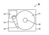
図18は、本発明のハードディスクドライブの一例を示す概略平面図である。図18に示されるハードディスクドライブ60は、上述した素子付サスペンション50と、素子付サスペンション50がデータの書き込みおよび読み込みを行うディスク51と、ディスク51を回転させるスピンドルモータ52と、素子付サスペンション50の素子を移動させるアーム53およびボイスコイルモータ54と、上記の部材を密閉するケース55とを有するものである。 FIG. 18 is a schematic plan view showing an example of the hard disk drive of the present invention. The
本発明のハードディスクドライブは、少なくとも素子付サスペンションを有し、通常は、さらにディスク、スピンドルモータ、アームおよびボイスコイルモータを有する。素子付サスペンションについては、上記「E.素子付サスペンション」に記載した内容と同様であるので、ここでの記載は省略する。また、その他の部材についても、一般的なハードディスクドライブに用いられる部材と同様のものを用いることができる。 The hard disk drive of the present invention has at least a suspension with an element, and usually further includes a disk, a spindle motor, an arm, and a voice coil motor. The suspension with an element is the same as that described in the above “E. As other members, the same members as those used in a general hard disk drive can be used.
なお、本発明は、上記実施形態に限定されるものではない。上記実施形態は例示であり、本発明の特許請求の範囲に記載された技術的思想と、実質的に同一の構成を有し、同様な作用効果を奏するものは、いかなる場合であっても本発明の技術的範囲に包含される。 The present invention is not limited to the above embodiment. The above-described embodiment is an exemplification, and the technical idea described in the claims of the present invention has substantially the same configuration and exhibits the same function and effect regardless of the case. It is included in the technical scope of the invention.
以下、実施例を用いて、本発明をさらに具体的に説明する。
[実施例1]
ポリイミド樹脂層(絶縁層)の上に、厚さ12μmの電解銅層(導体層)を有する積層部材を準備した。次に、電解銅層の表面に、アクリル系のDFRをラミネートし、露光および現像を行い、レジストパターンを形成した。レジストパターンの開口幅は10μmであり、ピッチは40μmであった。次に、塩化鉄系エッチング液を用いて、レジストパターンから露出する電解銅層をウェットエッチングした。これにより、頂面での幅が5μm、底面での幅が13μmの第一配線部を形成した。Hereinafter, the present invention will be described more specifically with reference to examples.
[Example 1]
A laminated member having an electrolytic copper layer (conductor layer) having a thickness of 12 μm was prepared on the polyimide resin layer (insulating layer). Next, an acrylic DFR was laminated on the surface of the electrolytic copper layer, and exposure and development were performed to form a resist pattern. The opening width of the resist pattern was 10 μm, and the pitch was 40 μm. Next, the electrolytic copper layer exposed from the resist pattern was wet etched using an iron chloride etching solution. As a result, a first wiring portion having a width of 5 μm at the top surface and a width of 13 μm at the bottom surface was formed.
その後、レジストパターンを残した状態で、第一配線部に給電しながら電解銅めっきを行い、第一配線部の側面に第二配線部を形成した。これにより、頂面での幅が7μm、底面での幅が15μmの配線層を有する回路基板を得た。第二配線部における底面および側面のなす角度θは、71.6°であった。また、隣り合う配線層の間隔は15μmであった。 Thereafter, electrolytic copper plating was performed while supplying power to the first wiring portion with the resist pattern remaining, thereby forming a second wiring portion on the side surface of the first wiring portion. As a result, a circuit board having a wiring layer having a width of 7 μm at the top surface and a width of 15 μm at the bottom surface was obtained. The angle θ formed between the bottom surface and the side surface in the second wiring portion was 71.6 °. The interval between adjacent wiring layers was 15 μm.
[実施例2]
第二配線部を形成するための電解銅めっきを長時間行ったこと以外は、実施例1と同様にして回路基板を得た。得られた回路基板の配線層は、頂面での幅が12μm、底面での幅が20μmであった。また、隣り合う配線層の間隔は10μmであった。
[実施例3]
まず、ポリイミド樹脂層(絶縁層)の上に、厚さ12μmの電解銅層(導体層)を有する積層部材を準備した。次に、電解銅層の表面に、アクリル系のDFRをラミネートし、露光および現像を行い、レジストパターンを形成した。レジストパターンの開口幅は10μmであり、ピッチは40μmであった。次に、塩化鉄系エッチング液を用いて、レジストパターンから露出する電解銅層をウェットエッチングした。これにより、頂面での幅が12μm、底面での幅が20μmの第一配線部を形成した。次に、第一配線部の断面形状を矩形に近づけるために、さらなるウェットエッチングを行い、頂面での幅が10μm、底面での幅が15μmの第一配線部を形成した。[Example 2]
A circuit board was obtained in the same manner as in Example 1 except that electrolytic copper plating for forming the second wiring part was performed for a long time. The wiring layer of the obtained circuit board had a width at the top surface of 12 μm and a width at the bottom surface of 20 μm. The interval between adjacent wiring layers was 10 μm.
[Example 3]
First, a laminated member having an electrolytic copper layer (conductor layer) having a thickness of 12 μm on a polyimide resin layer (insulating layer) was prepared. Next, an acrylic DFR was laminated on the surface of the electrolytic copper layer, and exposure and development were performed to form a resist pattern. The opening width of the resist pattern was 10 μm, and the pitch was 40 μm. Next, the electrolytic copper layer exposed from the resist pattern was wet etched using an iron chloride etching solution. As a result, a first wiring portion having a width of 12 μm at the top surface and a width of 20 μm at the bottom surface was formed. Next, in order to make the cross-sectional shape of the first wiring part close to a rectangle, further wet etching was performed to form a first wiring part having a top surface width of 10 μm and a bottom surface width of 15 μm.
その後、レジストパターンを残した状態で、第一配線部に給電しながら電解銅めっきを行い、第一配線部の側面に第二配線部を形成した。これにより、頂面での幅が15μm、底面での幅が20μmの配線層を有する回路基板を得た。第二配線部における底面および側面のなす角度θは、78.2°であった。また、隣り合う配線層の間隔は20μmであった。 Thereafter, electrolytic copper plating was performed while supplying power to the first wiring portion with the resist pattern remaining, thereby forming a second wiring portion on the side surface of the first wiring portion. As a result, a circuit board having a wiring layer having a width of 15 μm at the top surface and a width of 20 μm at the bottom surface was obtained. The angle θ formed between the bottom surface and the side surface in the second wiring portion was 78.2 °. The interval between adjacent wiring layers was 20 μm.
[実施例4]
第二配線部を形成するための電解銅めっきを長時間行ったこと以外は、実施例3と同様にして回路基板を得た。得られた回路基板の配線層は、頂面での幅が20μm、底面での幅が25μmであった。また、隣り合う配線層の間隔は15μmであった。[Example 4]
A circuit board was obtained in the same manner as in Example 3 except that electrolytic copper plating for forming the second wiring part was performed for a long time. The obtained wiring layer of the circuit board had a width at the top surface of 20 μm and a width at the bottom surface of 25 μm. The interval between adjacent wiring layers was 15 μm.
[実施例5〜8]
レジストパターンを除去した状態で、第一配線部に給電しながら電解銅めっきを行い、第一配線部の頂面および側面に第三配線部を形成したこと以外は、実施例1〜4と同様にして回路基板を得た。[Examples 5 to 8]
With the resist pattern removed, electrolytic copper plating is performed while supplying power to the first wiring portion, and the third wiring portion is formed on the top surface and the side surface of the first wiring portion. Thus, a circuit board was obtained.
1…金属支持基板、 2…絶縁層、 3…配線層、 3a…第一配線部、 3b…第二配線部、 4…カバー層、 5…保護めっき部、 6…レジストパターン、 7…ウェットエッチング、 8…スプレー装置、 11…素子実装領域、 12…外部回路基板接続領域、 13…配線層、 20…サスペンション用基板 DESCRIPTION OF SYMBOLS 1 ... Metal support substrate, 2 ... Insulating layer, 3 ... Wiring layer, 3a ... First wiring part, 3b ... Second wiring part, 4 ... Cover layer, 5 ... Protection plating part, 6 ... Resist pattern, 7 ...
Claims (18)
Translated fromJapanese前記配線層が、第一配線部と、前記第一配線部の側面にめっき法により形成された第二配線部とを有し、前記第一配線部および前記第二配線部の頂面の位置が一致していることを特徴とする回路基板。A circuit board having an insulating layer and a wiring layer formed on the insulating layer,
The wiring layer has a first wiring part and a second wiring part formed by plating on a side surface of the first wiring part, and the positions of the top surfaces of the first wiring part and the second wiring part A circuit board characterized by matching.
前記配線層が、第一配線部と、前記第一配線部の側面および頂面にめっき法により形成され、前記第一配線部と同一材料の第三配線部とを有することを特徴とする回路基板。A circuit board having an insulating layer and a wiring layer formed on the insulating layer,
The wiring layer includes a first wiring portion, and a third wiring portion formed of a plating method on a side surface and a top surface of the first wiring portion and made of the same material as the first wiring portion. substrate.
前記配線層を形成するための導体層の表面にレジストパターンを形成し、前記レジストパターンから露出する前記導体層を、前記レジストパターンの裏面が露出するようにウェットエッチングし、第一配線部を形成する第一配線部形成工程と、
前記レジストパターンを残した状態で、前記第一配線部の側面に、めっき法により第二配線部を形成する第二配線部形成工程と、
を有することを特徴とする回路基板の製造方法。A method of manufacturing a circuit board having an insulating layer and a wiring layer formed on the insulating layer,
A resist pattern is formed on the surface of the conductor layer for forming the wiring layer, and the conductor layer exposed from the resist pattern is wet-etched so that the back surface of the resist pattern is exposed to form a first wiring portion. A first wiring part forming step,
With the resist pattern left, a second wiring portion forming step for forming a second wiring portion by plating on the side surface of the first wiring portion;
A method of manufacturing a circuit board, comprising:
前記配線層を形成するための導体層の表面にレジストパターンを形成し、前記レジストパターンから露出する前記導体層を、前記レジストパターンの裏面が露出するようにウェットエッチングし、第一配線部を形成する第一配線部形成工程と、
前記レジストパターンを除去した状態で、前記第一配線部の側面および頂面に、めっき法により、前記第一配線部と同一材料の第三配線部を形成する第三配線部形成工程と、
を有することを特徴とする回路基板の製造方法。A method of manufacturing a circuit board having an insulating layer and a wiring layer formed on the insulating layer,
A resist pattern is formed on the surface of the conductor layer for forming the wiring layer, and the conductor layer exposed from the resist pattern is wet-etched so that the back surface of the resist pattern is exposed to form a first wiring portion. A first wiring part forming step,
In a state where the resist pattern has been removed, a third wiring part forming step for forming a third wiring part of the same material as the first wiring part by plating on the side surface and the top surface of the first wiring part,
A method of manufacturing a circuit board, comprising:
Priority Applications (1)
| Application Number | Priority Date | Filing Date | Title |
|---|---|---|---|
| JP2010161803AJP2012023296A (en) | 2010-07-16 | 2010-07-16 | Circuit board, method of manufacturing the same, substrate for suspension, suspension, suspension with element and hard disk drive |
Applications Claiming Priority (1)
| Application Number | Priority Date | Filing Date | Title |
|---|---|---|---|
| JP2010161803AJP2012023296A (en) | 2010-07-16 | 2010-07-16 | Circuit board, method of manufacturing the same, substrate for suspension, suspension, suspension with element and hard disk drive |
Publications (1)
| Publication Number | Publication Date |
|---|---|
| JP2012023296Atrue JP2012023296A (en) | 2012-02-02 |
Family
ID=45777281
Family Applications (1)
| Application Number | Title | Priority Date | Filing Date |
|---|---|---|---|
| JP2010161803APendingJP2012023296A (en) | 2010-07-16 | 2010-07-16 | Circuit board, method of manufacturing the same, substrate for suspension, suspension, suspension with element and hard disk drive |
Country Status (1)
| Country | Link |
|---|---|
| JP (1) | JP2012023296A (en) |
Cited By (11)
| Publication number | Priority date | Publication date | Assignee | Title |
|---|---|---|---|---|
| JP2016146334A (en)* | 2015-01-29 | 2016-08-12 | 大日本印刷株式会社 | Vehicle with heating plate, conductive pattern sheet and heating plate |
| JP2017111937A (en)* | 2015-12-16 | 2017-06-22 | 大日本印刷株式会社 | Heating electrode device, electrically heated glass, and vehicle |
| JP2017130402A (en)* | 2016-01-22 | 2017-07-27 | 大日本印刷株式会社 | Current-carrying heating glass and vehicle |
| JP2017130388A (en)* | 2016-01-21 | 2017-07-27 | 大日本印刷株式会社 | Heating electrode device, energized heating glass, and vehicle |
| JP2017130389A (en)* | 2016-01-21 | 2017-07-27 | 大日本印刷株式会社 | Electrically heated glass, and vehicle |
| US10912155B2 (en) | 2014-11-17 | 2021-02-02 | Dai Nippon Printing Co., Ltd. | Heating plate, conductive pattern sheet, vehicle, and method of manufacturing heating plate |
| JPWO2022030645A1 (en)* | 2020-08-07 | 2022-02-10 | ||
| WO2022030644A1 (en)* | 2020-08-07 | 2022-02-10 | 東洋鋼鈑株式会社 | Copper-clad layered body and method for producing same |
| US11338774B2 (en) | 2014-11-17 | 2022-05-24 | Dai Nippon Printing Co., Ltd. | Heating plate, conductive pattern sheet, vehicle, and method of manufacturing heating plate |
| JPWO2022201563A1 (en)* | 2021-03-25 | 2022-09-29 | ||
| US12439483B2 (en) | 2015-11-17 | 2025-10-07 | Dai Nippon Printing Co., Ltd. | Heat-generating plate |
- 2010
- 2010-07-16JPJP2010161803Apatent/JP2012023296A/enactivePending
Cited By (13)
| Publication number | Priority date | Publication date | Assignee | Title |
|---|---|---|---|---|
| US11338774B2 (en) | 2014-11-17 | 2022-05-24 | Dai Nippon Printing Co., Ltd. | Heating plate, conductive pattern sheet, vehicle, and method of manufacturing heating plate |
| US10912155B2 (en) | 2014-11-17 | 2021-02-02 | Dai Nippon Printing Co., Ltd. | Heating plate, conductive pattern sheet, vehicle, and method of manufacturing heating plate |
| JP2016146334A (en)* | 2015-01-29 | 2016-08-12 | 大日本印刷株式会社 | Vehicle with heating plate, conductive pattern sheet and heating plate |
| US12439483B2 (en) | 2015-11-17 | 2025-10-07 | Dai Nippon Printing Co., Ltd. | Heat-generating plate |
| JP2017111937A (en)* | 2015-12-16 | 2017-06-22 | 大日本印刷株式会社 | Heating electrode device, electrically heated glass, and vehicle |
| JP2017130388A (en)* | 2016-01-21 | 2017-07-27 | 大日本印刷株式会社 | Heating electrode device, energized heating glass, and vehicle |
| JP2017130389A (en)* | 2016-01-21 | 2017-07-27 | 大日本印刷株式会社 | Electrically heated glass, and vehicle |
| JP2017130402A (en)* | 2016-01-22 | 2017-07-27 | 大日本印刷株式会社 | Current-carrying heating glass and vehicle |
| JPWO2022030645A1 (en)* | 2020-08-07 | 2022-02-10 | ||
| US12402253B2 (en) | 2020-08-07 | 2025-08-26 | Toyo Kohan Co., Ltd. | Copper clad laminate and method for producing the same |
| JP7738563B2 (en) | 2020-08-07 | 2025-09-12 | 東洋鋼鈑株式会社 | Copper clad laminate and method for manufacturing same |
| WO2022030644A1 (en)* | 2020-08-07 | 2022-02-10 | 東洋鋼鈑株式会社 | Copper-clad layered body and method for producing same |
| JPWO2022201563A1 (en)* | 2021-03-25 | 2022-09-29 |
Similar Documents
| Publication | Publication Date | Title |
|---|---|---|
| JP2012023296A (en) | Circuit board, method of manufacturing the same, substrate for suspension, suspension, suspension with element and hard disk drive | |
| JP2013145628A (en) | Method for manufacturing suspension substrate | |
| JP4784695B2 (en) | Magnetic head suspension and manufacturing method | |
| JP2011198402A (en) | Flexure substrate for suspension, suspension, suspension with head, and hard disk drive | |
| JP5651933B2 (en) | Suspension substrate and manufacturing method thereof | |
| JP6497853B2 (en) | Wiring circuit board and manufacturing method thereof | |
| JP2008276922A (en) | Suspension board, suspension, suspension with head and hard disk | |
| US20110235213A1 (en) | Suspension substrate, manufacturing method of suspension substrate, suspension, device-mounted suspension, and hard disk drive | |
| JP6174838B2 (en) | Suspension substrate, suspension, suspension with element, hard disk drive, and manufacturing method of suspension substrate | |
| JP6576651B2 (en) | Wiring circuit board and manufacturing method thereof | |
| JP2008276923A (en) | Suspension board, suspension, suspension with head and hard disk | |
| JP5174785B2 (en) | Printed circuit board | |
| JP2013206488A (en) | Substrate for suspension, suspension, element equipping suspension, hard disc drive, and manufacturing method of substrate for suspension | |
| JP5728837B2 (en) | Suspension substrate, method for manufacturing suspension substrate, suspension, suspension with element, and hard disk drive | |
| US8673160B1 (en) | Electrical interconnect with improved corrosion resistance for a disk drive head suspension | |
| JP5131604B2 (en) | Suspension substrate and method for manufacturing suspension substrate | |
| JP5724278B2 (en) | Suspension substrate, method for manufacturing suspension substrate, suspension, suspension with element, and hard disk drive | |
| JP5482465B2 (en) | Manufacturing method of flexure substrate for suspension | |
| JP5729006B2 (en) | Suspension substrate, suspension, suspension with head, hard disk drive, and method for manufacturing suspension substrate | |
| JP5640600B2 (en) | Flexure substrate for suspension, suspension, suspension with head, hard disk drive, and method for manufacturing suspension flexure substrate | |
| JP4992648B2 (en) | Suspension board and manufacturing method thereof | |
| JP2016184455A (en) | Suspension substrate, suspension, suspension with element, hard disk drive, and manufacturing method of suspension substrate | |
| JP2006005228A (en) | WIRING BOARD, MAGNETIC DISK DEVICE, AND WIRING BOARD MANUFACTURING METHOD | |
| JP5793897B2 (en) | Suspension substrate, suspension, suspension with element, hard disk drive, and manufacturing method of suspension substrate | |
| JP6139059B2 (en) | Suspension substrate, suspension, suspension with element, hard disk drive, and manufacturing method of suspension substrate |