JP2012018619A - Detection device and display device - Google Patents
Detection device and display deviceDownload PDFInfo
- Publication number
- JP2012018619A JP2012018619AJP2010156894AJP2010156894AJP2012018619AJP 2012018619 AJP2012018619 AJP 2012018619AJP 2010156894 AJP2010156894 AJP 2010156894AJP 2010156894 AJP2010156894 AJP 2010156894AJP 2012018619 AJP2012018619 AJP 2012018619A
- Authority
- JP
- Japan
- Prior art keywords
- unit
- detection
- detection electrodes
- signal
- oscillation
- Prior art date
- Legal status (The legal status is an assumption and is not a legal conclusion. Google has not performed a legal analysis and makes no representation as to the accuracy of the status listed.)
- Granted
Links
Images


Classifications
- G—PHYSICS
- G06—COMPUTING OR CALCULATING; COUNTING
- G06F—ELECTRIC DIGITAL DATA PROCESSING
- G06F3/00—Input arrangements for transferring data to be processed into a form capable of being handled by the computer; Output arrangements for transferring data from processing unit to output unit, e.g. interface arrangements
- G06F3/01—Input arrangements or combined input and output arrangements for interaction between user and computer
- G06F3/03—Arrangements for converting the position or the displacement of a member into a coded form
- G06F3/041—Digitisers, e.g. for touch screens or touch pads, characterised by the transducing means
- G06F3/0412—Digitisers structurally integrated in a display
- G—PHYSICS
- G06—COMPUTING OR CALCULATING; COUNTING
- G06F—ELECTRIC DIGITAL DATA PROCESSING
- G06F3/00—Input arrangements for transferring data to be processed into a form capable of being handled by the computer; Output arrangements for transferring data from processing unit to output unit, e.g. interface arrangements
- G06F3/01—Input arrangements or combined input and output arrangements for interaction between user and computer
- G06F3/03—Arrangements for converting the position or the displacement of a member into a coded form
- G06F3/041—Digitisers, e.g. for touch screens or touch pads, characterised by the transducing means
- G06F3/044—Digitisers, e.g. for touch screens or touch pads, characterised by the transducing means by capacitive means
- G06F3/0445—Digitisers, e.g. for touch screens or touch pads, characterised by the transducing means by capacitive means using two or more layers of sensing electrodes, e.g. using two layers of electrodes separated by a dielectric layer
- G—PHYSICS
- G06—COMPUTING OR CALCULATING; COUNTING
- G06F—ELECTRIC DIGITAL DATA PROCESSING
- G06F3/00—Input arrangements for transferring data to be processed into a form capable of being handled by the computer; Output arrangements for transferring data from processing unit to output unit, e.g. interface arrangements
- G06F3/01—Input arrangements or combined input and output arrangements for interaction between user and computer
- G06F3/03—Arrangements for converting the position or the displacement of a member into a coded form
- G06F3/041—Digitisers, e.g. for touch screens or touch pads, characterised by the transducing means
- G06F3/044—Digitisers, e.g. for touch screens or touch pads, characterised by the transducing means by capacitive means
- G06F3/0446—Digitisers, e.g. for touch screens or touch pads, characterised by the transducing means by capacitive means using a grid-like structure of electrodes in at least two directions, e.g. using row and column electrodes
Landscapes
- Engineering & Computer Science (AREA)
- General Engineering & Computer Science (AREA)
- Theoretical Computer Science (AREA)
- Human Computer Interaction (AREA)
- Physics & Mathematics (AREA)
- General Physics & Mathematics (AREA)
- Position Input By Displaying (AREA)
- Liquid Crystal (AREA)
- Liquid Crystal Display Device Control (AREA)
- Control Of Indicators Other Than Cathode Ray Tubes (AREA)
Abstract
Description
Translated fromJapanese本発明は、指、手、腕、ペンなどの物体(以下「指など」という)が検出面に触れた位置を検知したり、指などが検出面から離れた場所にいるときにその物体の空間位置を検知したり、または、物体の検出面上の動きを検知したりすることの可能な検知装置に関する。また、本発明は、そのような検知装置を備えた表示装置に関する。 The present invention detects a position where an object such as a finger, hand, arm, or pen (hereinafter referred to as a “finger”) touches the detection surface, or when the finger is located away from the detection surface. The present invention relates to a detection device capable of detecting a spatial position or detecting movement of an object on a detection surface. The present invention also relates to a display device including such a detection device.
従来から、指などで触れることにより情報を入力する技術が知られている。その中でも特に注目されている技術として、ディスプレイに表示された種々のボタンを指などで触れることにより、通常のボタンを指などで押した場合と同様の情報入力を可能とする表示装置がある(特許文献1,2参照)。この技術は、ディスプレイとボタンの共用化を可能にすることから、省スペース化や部品点数の削減という大きなメリットをもたらす。 Conventionally, a technique for inputting information by touching with a finger or the like is known. Among them, there is a display device capable of inputting information similar to a case where a normal button is pressed with a finger or the like by touching various buttons displayed on the display with a finger or the like as a technology that is particularly attracting attention ( (See
指などの接触を検出するタッチセンサには、種々のタイプのものが存在するが、一般に普及しているものとして、例えば、静電容量タイプのものが挙げられる(特許文献2参照)。このタイプのものは、指などでタッチパネルに接触することによってパネルの表面電界に生じる変化を検出電極に流れる電流の周波数の変化で捕らえ、指などの接触を検出するようになっている。 There are various types of touch sensors that detect contact with a finger or the like, and examples of commonly used touch sensors include a capacitance type sensor (see Patent Document 2). In this type, a change in the surface electric field of the panel by touching the touch panel with a finger or the like is captured by a change in the frequency of the current flowing in the detection electrode, and the contact with the finger or the like is detected.
上記の検出方式は、タッチパネルの表面電界の変化を検出電極に流れる電流の周波数の変化で読み取る方式となっている。そのため、指などがタッチパネルの表面に接触するか、または十分に近接していることが必要となり、指などが表面から遠く離れている時(例えば、表面から1cm以上離れている時)には、タッチパネルに情報が入力されない。しかし、例えば、特許文献3に記載されているように、物体の空間位置に応じて、隣り合う検知電極同士の間隔を変更することにより、指などが表面から遠く離れている時であっても、タッチパネルへ情報を入力することが可能となる。上記特許文献3では、隣り合う検知電極同士の間隔の変更は、スキャンする検知電極を間引くことにより行われている。 The above detection method is a method of reading a change in the surface electric field of the touch panel by a change in the frequency of the current flowing through the detection electrode. Therefore, it is necessary that a finger or the like is in contact with or sufficiently close to the surface of the touch panel. When the finger or the like is far from the surface (for example, 1 cm or more away from the surface), Information is not entered on the touch panel. However, as described in
ところで、上記の検出方式では、検知電極を駆動している最中に、指などが検知電極に接近すると、検知電極に電荷が溜まってしまうことがある。この場合、溜まった電荷量に応じて検知電極の静電容量が変化するので、検出感度が不安定になってしまうことがあるという問題があった。 By the way, in the above detection method, when a finger or the like approaches the detection electrode while the detection electrode is being driven, electric charges may accumulate in the detection electrode. In this case, there is a problem that the detection sensitivity may become unstable because the capacitance of the detection electrode changes according to the amount of accumulated charge.
本発明はかかる問題点に鑑みてなされたものであり、その目的は、検知電極を駆動している最中の検出感度を安定にすることの可能な検知装置およびそれを備えた表示装置を提供することにある。 The present invention has been made in view of such problems, and an object thereof is to provide a detection device capable of stabilizing detection sensitivity during driving of the detection electrode and a display device including the same. There is to do.
本発明の検知装置は、複数の検知電極が検出面に配置されたセンサ部と、複数の検知電極のうち1または複数の電極を選択する選択部と、選択部により選択された1または複数の検知電極に生じた容量により発振周波数が決まる発振部とを備えている。この検知装置は、さらに、発振部からの信号の周波数に対応する信号を出力する変換部と、発振部と選択部とをつなぐ配線と定電圧線との電気的な継断を行うスイッチ部とを備えている。 The detection device of the present invention includes a sensor unit in which a plurality of detection electrodes are arranged on a detection surface, a selection unit that selects one or a plurality of electrodes among the plurality of detection electrodes, and one or more selected by the selection unit And an oscillation unit whose oscillation frequency is determined by the capacitance generated in the detection electrode. The detection device further includes a conversion unit that outputs a signal corresponding to the frequency of the signal from the oscillation unit, a switch unit that electrically connects the wiring connecting the oscillation unit and the selection unit, and the constant voltage line. It has.
本発明の表示装置は、映像信号に基づいて表示面に画像を表示する表示パネルと、上記の検知装置とを備えたものである。具体的には、この表示装置は、上記の表示パネルと、複数の検知電極が表示面に配置されたセンサ部と、複数の検知電極のうち1または複数の電極を選択する選択部と、選択部により選択された1または複数の検知電極に生じた容量により発振周波数が決まる発振部とを備えている。この表示装置は、さらに、発振部からの信号の周波数に対応する信号を出力する変換部と、発振部と選択部とをつなぐ配線と定電圧線との電気的な継断を行うスイッチ部とを備えている。 The display device of the present invention includes a display panel that displays an image on a display surface based on a video signal, and the detection device. Specifically, the display device includes the display panel, a sensor unit in which a plurality of detection electrodes are arranged on a display surface, a selection unit that selects one or a plurality of electrodes among the plurality of detection electrodes, and a selection And an oscillation unit whose oscillation frequency is determined by the capacitance generated in one or a plurality of detection electrodes selected by the unit. The display device further includes a conversion unit that outputs a signal corresponding to the frequency of the signal from the oscillation unit, a switch unit that electrically disconnects a wiring connecting the oscillation unit and the selection unit, and a constant voltage line. It has.
本発明の検知装置および表示装置において、変換部および発振部の少なくとも一方がイネーブルまたはディスエーブルに状態を変化させることが可能となっていてもよい。その場合に、本発明の検知装置および表示装置が、発振部および変換部のうち上述の状態変化を制御する制御部をさらに備えていてもよい。例えば、変換部がイネーブルまたはディスエーブルに状態を変化させることが可能となっている場合に、制御部は、例えば、選択部が1または複数の検知電極を選択している間に、変換部をディスエーブルにするとともに、選択部が選択している1または複数の検知電極を定電圧線に接続させるようになっていてもよい。また、例えば、発振部がイネーブルまたはディスエーブルに状態を変化させることが可能となっている場合に、制御部は、例えば、選択部が1または複数の検知電極を選択している間に、発振部をディスエーブルにするとともに、選択部が選択している1または複数の検知電極を定電圧線に接続させるようになっていてもよい。また、本発明の表示装置において、検知装置は、表示パネルと一体に形成されていてもよいし、表示パネルと別体に形成されていてもよい。 In the detection device and the display device of the present invention, at least one of the conversion unit and the oscillation unit may be enabled or disabled. In that case, the detection device and the display device of the present invention may further include a control unit that controls the above-described state change among the oscillation unit and the conversion unit. For example, when it is possible to change the state of the conversion unit to enable or disable, the control unit may change the conversion unit while the selection unit is selecting one or more detection electrodes. While being disabled, one or a plurality of detection electrodes selected by the selection unit may be connected to the constant voltage line. In addition, for example, when the oscillation unit can change the state to enable or disable, the control unit oscillates while the selection unit selects one or a plurality of detection electrodes, for example. The part may be disabled, and one or a plurality of detection electrodes selected by the selection part may be connected to the constant voltage line. In the display device of the present invention, the detection device may be formed integrally with the display panel, or may be formed separately from the display panel.
本発明の検知装置および表示装置では、発振部と選択部とをつなぐ配線と定電圧線との電気的な継断を行うスイッチ部が設けられている。これにより、検知電極を駆動している最中に、スイッチ部で電気的な継断を実行することにより、検知電極に溜まった電荷がスイッチ部を介して定電圧線に放出される。 In the detection device and the display device of the present invention, a switch unit that electrically connects and disconnects the wiring connecting the oscillation unit and the selection unit and the constant voltage line is provided. As a result, when the detection electrode is driven, electrical switching is performed at the switch unit, whereby the charge accumulated in the detection electrode is released to the constant voltage line through the switch unit.
例えば、変換部がイネーブルまたはディスエーブルに状態を変化させることが可能となっている場合に、変換部がディスエーブルとなっている間に、検知装置および表示装置に設けられた制御部がスイッチ部をオンする。また、例えば、発振部がイネーブルまたはディスエーブルに状態を変化させることが可能となっている場合に、発振部がディスエーブルとなっている間に、検知装置および表示装置に設けられた制御部がスイッチ部をオンする。このようにすることで、選択部が選択している1または複数の検知電極が、スイッチ部を介して定電圧線に接続され、検知電極に溜まった電荷がスイッチ部を介して定電圧線に放出される。 For example, when it is possible to change the state of the conversion unit to enable or disable, the control unit provided in the detection device and the display device is switched to the switch unit while the conversion unit is disabled. Turn on. In addition, for example, when the oscillation unit can be changed to enable or disable, while the oscillation unit is disabled, the control unit provided in the detection device and the display device Turn on the switch. In this way, one or more detection electrodes selected by the selection unit are connected to the constant voltage line via the switch unit, and the charge accumulated in the detection electrode is transferred to the constant voltage line via the switch unit. Released.
本発明の検知装置および表示装置によれば、検知電極に溜まった電荷を、スイッチ部を介して定電圧線に放出するようにしたので、検知電極への電荷溜まりをなくすことができる。その結果、検知電極の静電容量が安定になるので、検知電極を駆動している最中の検出感度を安定にすることができる。 According to the detection device and the display device of the present invention, since the charge accumulated in the detection electrode is discharged to the constant voltage line via the switch unit, the charge accumulation in the detection electrode can be eliminated. As a result, since the capacitance of the detection electrode becomes stable, the detection sensitivity during driving of the detection electrode can be stabilized.
以下、発明を実施するための形態について、図面を参照して詳細に説明する。なお、説明は以下の順序で行う。
1.接触検知および近接検知の基本原理(図1)
2.第1の実施の形態(図2〜図9)
液晶表示パネルとタッチパネルが別体となっている例
3.第2の実施の形態(図10〜図12)
液晶表示パネルとタッチパネルが一体となっている例
4.変形例(図13)
発振部の温度特性による周波数の変化を補正する例など
DESCRIPTION OF EMBODIMENTS Hereinafter, embodiments for carrying out the invention will be described in detail with reference to the drawings. The description will be given in the following order.
1. Basic principle of contact detection and proximity detection (Figure 1)
2. First embodiment (FIGS. 2 to 9)
2. An example in which the liquid crystal display panel and the touch panel are separated. Second Embodiment (FIGS. 10 to 12)
3. An example in which a liquid crystal display panel and a touch panel are integrated. Modified example (FIG. 13)
Example of correcting frequency change due to temperature characteristics of oscillator
<1.接触検知および近接検知の基本原理>
最初に、以下の実施の形態の表示装置で用いられる接触検知および近接検知の基本原理について説明する。図1は、接触検知および近接検知を行うことの可能な検知装置100の構成例を表したものである。<1. Basic principles of contact detection and proximity detection>
First, the basic principle of contact detection and proximity detection used in the display devices of the following embodiments will be described. FIG. 1 illustrates a configuration example of a detection device 100 capable of performing contact detection and proximity detection.
検知装置100は、静電容量型の検知装置であり、例えば、図1に示したように、2次元電極110を備えている。2次元電極110は、検出面(図示せず)に形成されたものであり、例えば、複数の検知電極110Hと、複数の検知電極110Vとにより構成されている。複数の検知電極110Hは、一の面内において、横方向に延在するとともに縦方向に所定の間隔で並列配置されている。複数の検知電極110Vは、複数の検知電極110Hの配置された面と平行な面内において、縦方向に延在するとともに横方向に所定の間隔で並列配置されている。 The detection device 100 is a capacitance-type detection device, and includes, for example, a two-
検知装置100は、2次元電極110の他に、2次元電極110の切り替え用のスイッチ素子120と、2次元電極110に交流信号を供給する信号源130と、周波数・電圧変換回路(F・V変換回路)140とを備えている。スイッチ素子120は、例えば、マルチプレクサである。マルチプレクサの一端側に設けられた複数の端子が、各検知電極110Hおよび各検知電極110Vの一端に1つずつ接続されており、マルチプレクサの他端側に設けられた1つの端子が信号源130およびF・V変換回路140に接続されている。 In addition to the two-
この検知装置100では、スイッチ素子120によって、例えば、複数の検知電極110Hが順次1つずつ選択されるとともに、複数の検知電極110Vが順次1つずつ選択される。これにより、信号源130の信号が複数の検知電極110Hに順次1つずつ印加されるとともに、複数の検知電極110Vに順次1つずつ印加される。また、この検知装置100では、スイッチ素子120によって、例えば、複数の検知電極110Hのうち所定の電極だけが順次1つずつ選択されるとともに、複数の検知電極110Vのうち所定の電極だけが順次1つずつ選択される。 In the detection device 100, for example, the plurality of
このとき、検出面に、例えば指など(図示せず)が接触したり、近接したりすると、検出面の表面電界が変化し、その変化が2次元電極110に流れる電流の周波数を変化させ、その周波数の変化がF・V変換回路140によって電圧の変化に変換される。この電圧変化を評価することにより、検出面における指などの接触位置や、検出面から離れた指などの空間位置、または検出面上の指などの動きを検出することができる。 At this time, for example, when a finger or the like (not shown) touches or approaches the detection surface, the surface electric field of the detection surface changes, and the change changes the frequency of the current flowing through the two-
<2.第1の実施の形態>
図2は、本発明の第1の実施の形態に係る表示装置1の概略構成の一例を表すものである。表示装置1は、タッチセンサ(および近接センサ)付きの表示装置であり、例えば、表示素子として液晶表示素子を備えており、さらに、この液晶表示素子の表面に静電容量型のタッチセンサ(および近接センサ)を液晶表示素子とは別体で備えている。<2. First Embodiment>
FIG. 2 shows an example of a schematic configuration of the
表示装置1は、例えば、図2に示したように、液晶表示パネル10、タッチパネル20、バックライト30、周辺回路40および検知回路50を備えている。タッチパネル20は、液晶表示パネル10の観察者側(正面)に配置されており、バックライト30は液晶表示パネル10の背後に配置されている。 For example, as shown in FIG. 2, the
[液晶表示パネル10]
液晶表示パネル10は、液晶分子の配列を変化させることにより光源(バックライト30)からの光を透過、変調させて映像表示を行うものである。この液晶表示パネル10は、例えば、映像信号40Aおよび同期信号40Bに応じて、マトリクス状に配置された複数の画素(図示せず)が周辺回路40によって駆動される透過型の表示パネルである。液晶表示パネル10は、例えば、行状に配置された複数の走査線WSL1と、列状に配置された複数の信号線DTLとを有している。各走査線WSL1と各信号線DTLとの交差部に対応して、複数の画素が行列状に配置されている。[Liquid Crystal Display Panel 10]
The liquid crystal display panel 10 displays images by transmitting and modulating light from a light source (backlight 30) by changing the arrangement of liquid crystal molecules. The liquid crystal display panel 10 is, for example, a transmissive display panel in which a plurality of pixels (not shown) arranged in a matrix are driven by a
[タッチパネル20]
タッチパネル20は、指などで、表示装置1の画像表示面20A(タッチパネル20の表面)に触れたり、指などを画像表示面60Aに近づけたり、指などを画像表示面60A上で動かしたりすることにより情報を入力するためのものである。このタッチパネル20は、例えば、液晶表示パネル10とは別体で設けられたものであり、例えば、液晶表示パネル10の表面に、接着剤(図示せず)などを介して貼り合わされている。このタッチパネル20は、上述した静電容量型のタッチセンサの一具体例に相当するものであり、XY(行列)マトリクスで接触・非接触を検出したり、空間位置を検出したり、動きを検出したりするものである。[Touch panel 20]
The
[バックライト30]
バックライト30は、液晶表示パネル10を背後から照明するものであり、例えば、導光板と、導光板の側面に配置された光源と、導光板の上面(光射出面)に配置された光学素子とを備えている。導光板は、光源からの光を導光板の上面に導くものであり、側面から入射した光を散乱し、均一化する機能を有している。光源は、線状光源であり、例えば、HCFL (Hot Cathode Fluorescent Lamp)、CCFL(Cold Cathode Fluorescent Lamp)、または複数のLED(Light Emitting Diode)を一列に配置したものなどからなる。光学素子は、例えば、拡散板、拡散シート、レンズフィルム、偏光分離シートなどを積層して構成されたものである。[Backlight 30]
The
[検知装置2]
図3は、表示装置1のうち、接触・非接触、空間位置、動きの検知に関与する部分(検知装置2)を抜き出したものである。検知装置2は、図1に例示した検知装置100と同様、接触検知および近接検知を行うことの可能な検知装置であり、例えば、図4に示したように、タッチパネル20および検知回路50を含んで構成されている。タッチパネル20は、例えば、センサ部21を有している。一方、検知回路50は、例えば、選択部51、発振部52、変換部53、制御部54、出力部55、および入力部56を含んで構成されている。[Detection device 2]
FIG. 3 shows an extracted part (detection device 2) of the
センサ部21は、指などの画像表示面20Aへの接触・非接触を検出したり、空間位置を検出したり、動きを検出したりするものである。センサ部21は、検出面である画像表示面20Aに形成されたものであり、例えば、図4に示したように、複数の検知電極21Hと、複数の検知電極21Vとにより構成されている。複数の検知電極21Hは、一の面内において、横方向に延在するとともに縦方向に所定の間隔で並列配置されている。複数の検知電極21Vは、複数の検知電極21Hの配置された面と平行な面内において、縦方向に延在するとともに横方向に所定の間隔で並列配置されている。 The
選択部51は、センサ部21内の各検知電極21H,21Vと、発振部52との電気的な継断を行うものである。具体的には、選択部51は、複数の検知電極21H,21Vのうち1または複数の電極を選択するとともに、選択した1または複数の検知電極21H,21Vと発振部52とを接続するようになっている。選択部51は、複数の検知電極21H(図4では4つの検知電極21H)の切り替え用のスイッチング素子51Aと、複数の検知電極21V(図4では4つの検知電極21V)の切り替え用のスイッチング素子51Bとを有している。 The
スイッチング素子51A,51Bは、それぞれ、例えば、マルチプレクサである。スイッチング素子51Aにおいて、マルチプレクサの一端側に設けられた複数の端子が走査線WSL2を介して各検知電極21Hの一端に1つずつ接続されており、マルチプレクサの他端側に設けられた1つの端子が配線を介して発振部52に接続されている。また、スイッチング素子51Bにおいて、マルチプレクサの一端側に設けられた複数の端子が走査線WSL3を介して各検知電極21Vの一端に1つずつ接続されており、マルチプレクサの他端側に設けられた1つの端子が配線を介して発振部52に接続されている。 Each of the
スイッチング素子51A,51Bは、制御部54から入力される選択信号およびEN信号(後述)に従って内部スイッチの切り替えを行うようになっている。スイッチング素子51A,51Bは、EN信号がイネーブルである場合は、センサ部21側の複数の端子のうち選択信号で選択された端子と、センサ部21とは反対側の端子とを電気的に接続するようになっている。また、スイッチング素子51A,51Bは、EN信号がディスエーブルである場合は、センサ部21側の全ての端子と、センサ部21とは反対側の端子とを電気的に開放するようになっている。 The
発振部52は、選択部51により選択された1または複数の検知電極21H,21Vに生じた容量により発振周波数が決まるようになっている。発振部52は、例えば、交流信号を発生する信号源52Aと、信号源52Aに並列接続された抵抗52Bと、互いに並列接続された信号源52Aおよび抵抗52Bの両端子のうち選択部51に接続された端子(以下、「端子A」と称する)に接続された容量素子52Cとを含んで構成されている。発振部52は、さらに、例えば、端子Aに接続されたスイッチ部52Dを含んで構成されている。発振部52は、端子Aおよびスイッチング素子51Aを介して各検知電極21Hに交流信号を印加するとともに、端子Aおよびスイッチング素子51Bを介して各検知電極21Vに交流信号を印加するようになっている。 The
スイッチ部52Dは、端子Aと定電圧線Lxとの電気的な継断を行うものであり、例えば、制御部54からの制御信号に応じてオンオフを変化させることが可能となっている。スイッチ部52Dは、少なくとも、各検知電極21Hまたは各検知電極21Vで、指などの画像表示面20Aへの接触・非接触を検出したり、空間位置を検出したり、動きを検出したりしている間は、オフ状態となっている。また、スイッチ部52Dは、後述するように、各検知電極21Hまたは各検知電極21Vに溜まった電荷を放出する際には、オン状態となっている。 The
変換部53は、発振部52からの信号の周波数に対応する信号を出力するものであり、例えば、図示しないが、クロックカウンタを含んで構成されている。クロックカウンタは、発振部52からの信号の周波数をカウントし、カウント数に応じたデジタル信号を出力するようになっている。さらに、変換部53は、制御部54から入力されるEN信号(後述)に従って、イネーブルまたはディスエーブルに状態を変化させることが可能となっている。 The converting
なお、変換部53は、F・V変換回路と、A/Dコンバータとを含んで構成されていてもよい。F・V変換回路は、発振部52からの信号を周波数に応じて電圧に変換するものである。F・V変換回路は、例えば、発振部52の出力端の信号を、その信号の周波数の大きさに応じた電圧値に変換し、その電圧値のアナログ信号を出力するようになっている。A/Dコンバータは、入力されたアナログ信号をデジタル信号に変換するものであり、例えば、F・V変換回路から出力されたアナログ信号をデジタル信号に変換するようになっている。 The
出力部55は、例えば、制御部54で導出された接触座標などを検知信号50Aとして出力するものである。入力部56は、例えば、検知回路50を駆動する際に使用する同期信号50Bや、画像表示面20Aに表示されるボタンなどの機能部分の座標を示す位置信号50Cなどの入力を受け付けるものである。 The
制御部54は、変換部53から入力された周波数に関する信号に基づいて、指などの接触座標、空間位置、または動きを導出するものである。また、制御部54は、選択部51に含まれる各スイッチング素子51A,51Bを制御するものである。制御部54は、選択部51が複数の検知電極21H,21Vのうち一部の電極だけを順次選択する選択信号を生成し選択部51(各スイッチング素子51A,51B)に印加するようになっている。具体的には、制御部54は、各スイッチング素子51A,51Bに対して、EN信号および選択信号を入力することにより、各スイッチング素子51A,51Bの内部スイッチの切り替えを行うようになっている。 The
制御部54は、例えば、所定のときに、スイッチング素子51AにEN信号としてディスエーブルを入力するようになっている。これにより、スイッチング素子51Aにおいて、センサ部21側の全ての端子と、センサ部21とは反対側の端子とが電気的に開放される。同様に、制御部54は、例えば、所定のときに、スイッチング素子51BにEN信号としてディスエーブルを入力するようになっている。これにより、スイッチング素子51Bにおいて、センサ部21側の全ての端子と、センサ部21とは反対側の端子とが電気的に開放される。 For example, the
また、制御部54は、例えば、所定のときに、スイッチング素子51Aに選択信号を入力するとともにEN信号としてイネーブルを入力するようになっている。これにより、スイッチング素子51Aにおいて、センサ部21側の複数の端子のうち選択信号で選択された端子と、センサ部21とは反対側の端子とが電気的に接続される。同様に、制御部54は、例えば、所定のときに、スイッチング素子51Bに選択信号を入力するとともにEN信号としてイネーブルを入力するようになっている。これにより、スイッチング素子51Bにおいて、センサ部21側の複数の端子のうち選択信号で選択された端子と、センサ部21とは反対側の端子とが電気的に接続される。 Further, for example, the
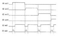
例えば、スイッチング素子51A,51Bのセンサ部21側の4つの端子に1つずつ順番にsel1,sel2,sel3,sel4という名称を付与したとすると、制御部54は、例えば、図5(A)に示したように、4つの端子sel1,sel2,sel3,sel4を1つずつ順番に選択するように、スイッチング素子51A,51Bに対して選択信号を入力するとともにEN信号としてイネーブルを入力するようになっている。 For example, if the names sel1, sel2, sel3, sel4 are given to the four terminals on the
制御部54は、発振部52に含まれるスイッチ部52Dと、変換部53とを制御するものでもある。具体的には、制御部54は、スイッチ部52Dおよび変換部53に対してEN信号(後述)を入力することにより、スイッチ部52Dおよび変換部53をイネーブルまたはディスエーブルに状態変化させることが可能となっている。 The
例えば、制御部54は、少なくとも、各検知電極21Hまたは各検知電極21Vで、指などの画像表示面20Aへの接触・非接触を検出したり、空間位置を検出したり、動きを検出したりしている間(例えば、スイッチング素子51Aまたは51Bがイネーブル状態となっており、かつ変換部53がイネーブル状態となっている間)は、スイッチ部52DにEN信号としてディスエーブルを入力し、スイッチ部52Dがオフ状態となるようになっている(図5(A)〜(C)参照)。このとき、選択部51が選択している1または複数の検知電極21H,21Vが発振部52に接続され、定電圧線Lxとは分離される。 For example, the
また、例えば、制御部54は、各検知電極21Hまたは各検知電極21Vに溜まった電荷を放出する間(例えば、スイッチング素子51Aまたは51Bがイネーブル状態となっており、かつ変換部53がディスエーブル状態となっている間)は、スイッチ部52DにEN信号としてイネーブルを入力し、スイッチ部52Dがオン状態となるようになっている(図5(A)〜(C)参照)。このとき、選択部51が選択している1または複数の検知電極21H,21Vがスイッチ部52Dを介して定電圧線Lxに接続される。 Further, for example, the
ところで、スイッチ部52DにEN信号としてイネーブルを入力するタイミングは、例えば、図5(A)〜(C)に示したように、選択部51が1または複数の検知電極21H,21Vを選択している間であって、かつ変換部53をイネーブルにする直前であることが好ましい。 By the way, the timing for inputting the enable signal as the EN signal to the
次に、本実施の形態の検知装置2における動作の一例について説明する。 Next, an example of the operation in the
[動作全体]
まず、例えば、表示装置1の電源投入、または検知装置2の起動により、制御部54は、検知装置2の動作を開始する。制御部54は、まず、スイッチング素子51Aまたは51BにEN信号としてイネーブルを入力するとともに、1または複数の検知電極21H,21Vを選択する選択信号を入力する。さらに、制御部54は、変換部53にEN信号としてディスエーブルを入力し、スイッチ部52DにEN信号としてイネーブルを入力する。これにより、選択信号によって選択された1または複数の検知電極21H,21Vと、定電圧線Lxとがスイッチ部52Dを介して接続される。その結果、定電圧線Lxに接続された1または複数の検知電極21H,21Vに溜まった電荷が、スイッチ部52Dを介して定電圧線Lxに放出され、定電圧線Lxに接続された1または複数の検知電極21H,21Vの電位が定電圧線Lxの電位となる。このとき、定電圧線Lxの電位がグラウンド電位となっている場合には、定電圧線Lxに接続された1または複数の検知電極21H,21Vの電位もグラウンド電位となる。なお、定電圧線Lxの電位がグラウンド電位とは異なる電位となっていてもよい。[Overall operation]
First, for example, when the
次に、制御部54は、スイッチ部52DにEN信号としてディスエーブルを入力する。これにより、選択信号によって選択された1または複数の検知電極21H,21Vが、定電圧線Lxから分離される。次に、制御部54は、変換部53にEN信号としてイネーブルを入力する。これにより、選択信号によって選択された1または複数の検知電極21H,21Vが、発振部52を介して変換部53に接続される。このとき、指などが画像表示面20Aに接近または接触していたとすると、指などの画像表示面20Aへの近接または接触などによって検知電極21H,21Vに生じた静電容量の変化が、発振部52の周波数の変化として、変換部53で検知される。変換部53で検知された周波数(または周波数の変化)は、制御部54に伝達され、制御部54は、変換部53で検知された周波数(または周波数の変化)の情報に基づいて、指などの接触座標、空間位置、または動きを導出する。制御部54は、導出した、指などの接触座標、空間位置、または動きについての情報を出力部55に入力し、出力部55は、入力された情報を、検知信号50Aとして外部に出力する。 Next, the
また、制御部54は、変換部53にEN信号としてイネーブルを入力する時間が所定の時間だけ経過すると、変換部53およびスイッチング素子51Aまたは51BにEN信号としてディスエーブルを入力する。その後は、制御部54は、検知電極21H,21Vの選択を順次変更しながら、上述の手順を繰り返し実行する。このようにして、本実施の形態の検知装置2において、指などの接触座標、空間位置、または動きが検出される。 In addition, when the time for inputting enable as the EN signal to the
[効果]
本実施の形態では、発振部52と選択部51とをつなぐ配線と定電圧線Lxとの電気的な継断を行うスイッチ部52Dが検知装置2に設けられている。これにより、検知電極21H,21Vを駆動している最中に、スイッチ部52Dで電気的な継断を実行することにより、検知電極21H,21Vに溜まった電荷がスイッチ部52Dを介して定電圧線Lxに放出される。例えば、変換部53がディスエーブルとなっている間に、制御部54がスイッチ部52Dをオンすることにより、選択部51が選択している1または複数の検知電極21H,21Vが、スイッチ部52Dを介して定電圧線Lxに接続され、検知電極21H,21Vに溜まった電荷がスイッチ部52Dを介して定電圧線Lxに放出される。その結果、検知電極21H,21Vへの電荷溜まりをなくすことができ、検知電極21H,21Vの静電容量が安定になるので、検知電極21H,21Vを駆動している最中の検出感度を安定にすることができる。[effect]
In the present embodiment, the
[変形例]
上記実施の形態では、変換部53がイネーブルまたはディスエーブルに状態を変化させることが可能となっていたが、例えば、図6に示したように、発振部52がイネーブルまたはディスエーブルに状態を変化させることが可能となっていてもよい。[Modification]
In the above embodiment, the
例えば、制御部54は、少なくとも、各検知電極21Hまたは各検知電極21Vで、指などの画像表示面20Aへの接触・非接触を検出したり、空間位置を検出したり、動きを検出したりしている間(例えば、スイッチング素子51Aまたは51Bがイネーブル状態となっており、かつ発振部52がイネーブル状態となっている間)は、スイッチ部52DにEN信号としてディスエーブルを入力し、スイッチ部52Dがオフ状態となるようになっている(図5(A)〜(C)参照)。このとき、選択部51が選択している1または複数の検知電極21H,21Vが発振部52に接続され、定電圧線Lxとは分離される。 For example, the
また、例えば、制御部54は、各検知電極21Hまたは各検知電極21Vに溜まった電荷を放出する間(例えば、スイッチング素子51Aまたは51Bがイネーブル状態となっており、かつ発振部52がディスエーブル状態となっている間)は、スイッチ部52DにEN信号としてイネーブルを入力し、スイッチ部52Dがオン状態となるようになっている(図5(A)〜(C)参照)。このとき、選択部51が選択している1または複数の検知電極21H,21Vがスイッチ部52Dを介して定電圧線Lxに接続される。 Further, for example, the
ところで、上記変形例において、スイッチ部52DにEN信号としてイネーブルを入力するタイミングは、例えば、選択部51が1または複数の検知電極21H,21Vを選択している間であって、かつ発振部52をイネーブルにする直前であることが好ましい。 By the way, in the above modification, the timing when the enable signal is input to the
また、上記実施の形態では、スイッチング素子51A,51Bが、マルチプレクサとなっていたが、例えば、図7、図8に示したように、複数のスイッチが互いに並列配置されたものであってもよい。この場合には、制御部54は、スイッチング素子51A,51Bに対して、EN信号および選択信号の代わりに、例えば、図9(A)〜(D)に示したように、スイッチング素子51A,51B内のスイッチごとにオンオフ制御信号を入力することが必要となる。 In the above embodiment, the
<3.第2の実施の形態>
図10は、本発明の第2の実施の形態に係る表示装置3の概略構成の一例を表すものである。表示装置3は、タッチセンサ(および近接センサ)付きの表示装置であり、例えば、表示素子として液晶表示素子を備えており、さらに、この液晶表示素子の表面に静電容量型のタッチセンサ(および近接センサ)を液晶表示素子と一体で備えている。表示装置3は、上記実施の形態およびその変形例に係る検知装置2と同様の構成を備えており、その点では、上記実施の形態およびその変形例に係る表示装置1の構成と共通している。<3. Second Embodiment>
FIG. 10 illustrates an example of a schematic configuration of the
表示装置3は、例えば、図10に示したように、タッチセンサ付き液晶表示パネル60、バックライト30、周辺回路40および検知回路50を備えている。バックライト30はタッチセンサ付き液晶表示パネル60の背後に配置されている。 For example, as shown in FIG. 10, the
[タッチセンサ付き液晶表示パネル60]
タッチセンサ付き液晶表示パネル60は、表示装置3の画像表示面60A(タッチセンサ付き液晶表示パネル60の表面)に映像を表示すると同時に、指などで、表示装置3の画像表示面60A(タッチセンサ付き液晶表示パネル60の表面)に触れたり、指などを画像表示面60Aに近づけたり、指などを画像表示面60A上で動かしたりすることにより情報を入力するためのものである。このタッチセンサ付き液晶表示パネル60は、XY(行列)マトリクスで接触・非接触を検出したり、空間位置を検出したり、動きを検出したりするものである。[
The liquid
図11は、タッチセンサ付き液晶表示パネル60の要部断面構成の一例を表すものである。タッチセンサ付き液晶表示パネル60は、液晶表示パネルに元々備えられている電極の一部(後述する共通電極43)および表示用駆動信号(後述するコモン駆動信号Vcom)を兼用して静電容量型タッチセンサを構成したものである。タッチセンサ付き液晶表示パネル60は、画素基板3と、画素基板3に対向して配置された対向基板4との間に液晶層5が挿設されたものである。 FIG. 11 illustrates an example of a cross-sectional configuration of a main part of the liquid
画素基板3は、回路基板としてのTFT基板31と、TFT基板31上にマトリクス状に配設された複数の画素電極22とを有する。TFT基板21には、各画素電極22を駆動するための図示しない表示ドライバやTFT(薄膜トランジスタ)の他、各画素電極に画像信号を供給するソース線や、各TFTを駆動するゲート線等の配線が形成されている。 The
対向基板4は、ガラス基板41と、ガラス基板41の一方の面に形成されたカラーフィルタ42と、カラーフィルタ42上に形成された共通電極43とを有する。カラーフィルタ42は、例えば、赤(R)、緑(G)、青(B)の3色のカラーフィルタ層を周期的に配列して構成したもので、表示画素(画素電極32)ごとにR、G、Bの3色が一組として対応付けられている。共通電極43は、タッチ検出動作を行うタッチセンサの一部を構成するセンサ用駆動電極としても兼用されるものである。 The
共通電極43は、コンタクト導電柱6によってTFT基板31と連結されている。このコンタクト導電柱6を介して、TFT基板31から共通電極43に交流矩形波形のコモン駆動信号Vcomが印加されるようになっている。このコモン駆動信号Vcomは、画素電極32に印加される画素電圧とともに各画素の表示電圧を画定するものであるが、タッチセンサの駆動信号としても兼用されるものである。即ち、このコモン駆動信号Vcomは、所定の周期ごとに極性反転するものとなっている。 The
ガラス基板41の他方の面には、センサ用検知電極44が形成され、更に、センサ用検知電極44の上には、偏光板45が配設されている。センサ用検知電極44は、タッチセンサの一部を構成するものである。液晶層5は、電界の状態に応じてそこを通過する光を変調するものであり、例えば、TN(ツイストネマティック)、VA(垂直配向)、ECB(電界制御複屈折)等の各種モードの液晶が用いられる。図11において、容量素子C1は、一の共通電極43と一のセンサ用検知電極44との間に形成される(静電)容量素子に対応するものである。 A
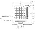
図12は、タッチセンサ付き液晶表示パネル60内のレイアウトの一例を表すものである。タッチセンサ付き液晶表示パネル60の面内の中央部分には、複数の共通電極43と、複数のセンサ用検知電極44とが互いに交差して配置されている。複数の共通電極43と、複数のセンサ用検知電極44とが互いに交差して配置されている部分(以下、「表示部分」と称する)が、画像表示面60Aに対応する部分である。タッチセンサ付き液晶表示パネル60の面内の外縁部分(すなわち、周辺ブラック)には、選択部51(スイッチング素子51A,51B)、発振部52、変換部53、周辺回路40、制御部54、出力部55、入力部56およびフレキシブルプリント配線板(FPC)57が配置されている。 FIG. 12 shows an example of the layout in the liquid
例えば、FPC57の一端が画素基板3の端縁に固定されており、FPC57の他端がタッチセンサ付き液晶表示パネル60からの出力信号を処理するデバイス(図示せず)に接続されるようになっている。FPC57は、可撓性のベースフィルムを有しており、このベースフィルムの一方の端部が画素基板3の端縁に固定されており、このベースフィルムの他方の端部は開放端となっている。 For example, one end of the FPC 57 is fixed to the edge of the
選択部51、発振部52、変換部53および周辺回路40は、上述の対向基板4上に配置されており、制御部54、出力部55、入力部56およびFPC57は、上述の画素基板3上に配置されている。具体的には、表示部分の一辺に沿ってスイッチング素子51Aが配置されており、表示部分の他の辺であって、かつスイッチング素子51Aが配置されている一辺に隣接する辺に沿ってスイッチング素子51Bが配置されている。表示部分の周縁のうち、スイッチング素子51Aの一端とスイッチング素子51Bの一端とが互いに近接する部分に、発振部52および変換部53が配置されている。このようなレイアウトにすることにより、センサ部21から発振部52までの配線を短くすることができる。 The
また、表示部分の周縁のうち、スイッチング素子51A,51Bの未配置の部分に、周辺回路40に含まれる共通電極ドライバ47および信号線セレクタ46が配置されている。さらに、画素基板3のうち対向基板4と非対向の部分に、制御部54、出力部55、入力部56およびFPC57が配置されている。 In addition, the common electrode driver 47 and the signal line selector 46 included in the
[効果]
本実施の形態では、上記実施の形態と同様、発振部52と選択部51とをつなぐ配線と定電圧線Lxとの電気的な継断を行うスイッチ部52Dが検知装置3に設けられている。これにより、検知電極21H,21Vを駆動している最中に、スイッチ部52Dで電気的な継断を実行することにより、検知電極21H,21Vに溜まった電荷がスイッチ部52Dを介して定電圧線Lxに放出される。例えば、変換部53がディスエーブルとなっている間に、制御部54がスイッチ部52Dをオンすることにより、選択部51が選択している1または複数の検知電極21H,21Vが、スイッチ部52Dを介して定電圧線Lxに接続され、検知電極21H,21Vに溜まった電荷がスイッチ部52Dを介して定電圧線Lxに放出される。その結果、検知電極21H,21Vへの電荷溜まりをなくすことができ、検知電極21H,21Vの静電容量が安定になるので、検知電極21H,21Vを駆動している最中の検出感度を安定にすることができる。[effect]
In the present embodiment, similarly to the above-described embodiment, the
また、本実施の形態では、センサ部21から発振部52までの配線が短くなっている。さらに、センサ部21、選択部51、発振部52、変換部53および周辺回路40が同一基板上に配置されており、ESD((Electro Static Discharge)対策用の保護回路が設けられていない。これにより、寄生容量の影響を低減することができるので、検出感度の低下を抑制することができる。 In the present embodiment, the wiring from the
<4.変形例>
以上、実施の形態ならびにその変形例を挙げて本発明を説明したが、本発明は実施の形態等に限定されるものではなく、種々の変形が可能である。<4. Modification>
While the present invention has been described with reference to the embodiment and its modifications, the present invention is not limited to the embodiment and the like, and various modifications are possible.
例えば、上記実施の形態等において、制御部54が、発振部52の温度特性による周波数の変化を補正するようになっていてもよい。例えば、図13に示したように、検知回路50に、変換部53および発振部52をさらに設け、発振部52に容量素子58を接続する。このとき、容量素子58の容量を、センサ部21側の変換部53で検出される周波数と同程度の周波数となるように調整しておく。また、容量素子58側の変換部53および発振部52が、指等が近付いて来たときに影響を受けないように、容量素子58側の変換部53および発振部52を、センサ部21から離れた場所や、電気的にシールドされている場所に配置する。このようにすることで、容量素子58側の発振部52では、当該発振部52の温度により周波数が変化する。これにより、制御部54は、容量素子58側の変換部53で検出された周波数を用いて、センサ部21の変換部53で検出された周波数に対して温度補正を施すことが可能となる。その結果、発振部52の温度特性による誤検出を抑制することができる。 For example, in the above-described embodiment or the like, the
また、上記実施の形態等では、液晶表示素子として透過型の素子を用いた場合について説明したが、透過型以外のもの、例えば、反射型の素子を用いることも可能である。ただし、その場合には、光源(バックライト30)をなくするか、または液晶表示素子の上面側に配置することが必要となる。 In the above-described embodiment and the like, the case where a transmissive element is used as the liquid crystal display element has been described. However, other than the transmissive element, for example, a reflective element can be used. However, in that case, it is necessary to eliminate the light source (backlight 30) or to dispose it on the upper surface side of the liquid crystal display element.
また、上記実施の形態等では、表示素子として液晶表示素子を用いた表示装置に対して本発明を適用した場合について説明したが、それ以外の表示素子、例えば有機EL素子を用いた表示装置にも適用可能である。 In the above-described embodiments and the like, the case where the present invention is applied to a display device using a liquid crystal display element as a display element has been described. However, the display device using other display elements, for example, organic EL elements, is used. Is also applicable.
また、上記実施の形態等において説明した一連の処理は、ハードウェアにより行うこともできるし、ソフトウェアにより行うこともできる。一連の処理をソフトウェアによって行う場合には、そのソフトウェアを構成するプログラムが、汎用のコンピュータ等にインストールされるようになっている。このようなプログラムは、コンピュータに内蔵されている記録媒体に予め記録しておくことも可能である。 In addition, the series of processing described in the above-described embodiments and the like can be performed by hardware or software. When a series of processing is performed by software, a program constituting the software is installed in a general-purpose computer or the like. Such a program can be recorded in advance in a recording medium built in the computer.
1,3…表示装置、2,100…検知装置、3…画素基板、4…対向基板、5…液晶層、6…コンタクト導電柱、10…液晶表示パネル、20…タッチパネル、20A,60A…画像表示面、21…センサ部、21H,21V,110H,110V…検知電極、30…バックライト、31…TFT基板、32…画素電極、40…周辺回路、40A…映像信号、40B,50B…同期信号、41…ガラス基板、42…カラーフィルタ、43…共通電極、44…センサ用検知電極、45…偏光板、46…信号線セレクタ、47…共通電極ドライバ、50…検知回路、50A…検知信号、50C…位置信号、51…選択部、51A,51B…スイッチング素子、52…発振部、52A…信号源、52B…抵抗、52C,58…容量素子、52D…スイッチ部、53…変換部、54…制御部、55…出力部、56…入力部、110…2次元電極、120…スイッチ素子、130…信号源、140…F・V変換回路、DTL…信号線、Lx…定電圧線、WSL,WSL1,WSL2,WSL3…走査線。 DESCRIPTION OF
Claims (7)
Translated fromJapanese前記複数の検知電極のうち1または複数の電極を選択する選択部と、
前記選択部により選択された1または複数の検知電極に生じた容量により発振周波数が決まる発振部と、
前記発振部からの信号の周波数に対応する信号を出力する変換部と、
前記発振部と前記選択部とをつなぐ配線と定電圧線との電気的な継断を行うスイッチ部と
を備えた検知装置。A sensor unit in which a plurality of detection electrodes are arranged on the detection surface;
A selection unit for selecting one or more of the plurality of detection electrodes;
An oscillation unit whose oscillation frequency is determined by a capacitance generated in one or a plurality of detection electrodes selected by the selection unit;
A converter that outputs a signal corresponding to the frequency of the signal from the oscillator;
A detection device comprising: a switch that performs electrical connection between a wiring connecting the oscillation unit and the selection unit and a constant voltage line.
請求項1に記載の検知装置。The detection device according to claim 1, wherein at least one of the conversion unit and the oscillation unit can change its state to enable or disable.
前記選択部が1または複数の検知電極を選択している間に、前記変換部をディスエーブルにするとともに、前記選択部が選択している1または複数の検知電極を前記定電圧線に接続させる制御部をさらに備えた
請求項2に記載の検知装置。The converter can change the state to enable or disable,
While the selection unit is selecting one or more detection electrodes, the conversion unit is disabled, and the one or more detection electrodes selected by the selection unit are connected to the constant voltage line. The detection device according to claim 2, further comprising a control unit.
請求項3に記載の検知装置。The control unit is one or more detection electrodes selected by the selection unit while the selection unit is selecting one or more detection electrodes and immediately before enabling the conversion unit. The detecting device according to claim 3, wherein the detecting device is connected to the constant voltage line.
前記選択部が1または複数の検知電極を選択している間に、前記発振部をディスエーブルにするとともに、前記選択部が選択している1または複数の検知電極を前記定電圧線に接続させる制御部をさらに備えた
請求項2に記載の検知装置。It is possible to change the state to enable or disable the oscillation unit,
While the selection unit selects one or a plurality of detection electrodes, the oscillation unit is disabled and the one or more detection electrodes selected by the selection unit are connected to the constant voltage line. The detection device according to claim 2, further comprising a control unit.
請求項5に記載の検知装置。The control unit is one or more detection electrodes selected by the selection unit while the selection unit is selecting one or more detection electrodes and immediately before enabling the oscillation unit. The detecting device according to claim 5, wherein the detecting device is connected to the constant voltage line.
複数の検知電極が前記表示面に配置されたセンサ部と、
前記複数の検知電極のうち1または複数の電極を選択する選択部と、
前記選択部により選択された1または複数の検知電極に生じた容量により発振周波数が決まる発振部と、
前記発振部からの信号の周波数に対応する信号を出力する変換部と、
前記発振部と前記選択部とをつなぐ配線と定電圧線との電気的な継断を行うスイッチ部と
を備えた表示装置。A display panel for displaying an image on a display surface based on a video signal;
A sensor unit in which a plurality of detection electrodes are arranged on the display surface;
A selection unit for selecting one or more of the plurality of detection electrodes;
An oscillation unit whose oscillation frequency is determined by a capacitance generated in one or a plurality of detection electrodes selected by the selection unit;
A converter that outputs a signal corresponding to the frequency of the signal from the oscillator;
A display device comprising: a switching unit that electrically connects a wiring connecting the oscillation unit and the selection unit to a constant voltage line.
Priority Applications (4)
| Application Number | Priority Date | Filing Date | Title |
|---|---|---|---|
| JP2010156894AJP5528926B2 (en) | 2010-07-09 | 2010-07-09 | Detection device and display device |
| TW100119871ATWI456444B (en) | 2010-07-09 | 2011-06-07 | Sensing device and display device |
| US13/067,637US8890836B2 (en) | 2010-07-09 | 2011-06-16 | Detection device and display apparatus with oscillation control |
| CN201110189448.9ACN102314255B (en) | 2010-07-09 | 2011-07-07 | Detection device and display device |
Applications Claiming Priority (1)
| Application Number | Priority Date | Filing Date | Title |
|---|---|---|---|
| JP2010156894AJP5528926B2 (en) | 2010-07-09 | 2010-07-09 | Detection device and display device |
Publications (2)
| Publication Number | Publication Date |
|---|---|
| JP2012018619Atrue JP2012018619A (en) | 2012-01-26 |
| JP5528926B2 JP5528926B2 (en) | 2014-06-25 |
Family
ID=45427478
Family Applications (1)
| Application Number | Title | Priority Date | Filing Date |
|---|---|---|---|
| JP2010156894AExpired - Fee RelatedJP5528926B2 (en) | 2010-07-09 | 2010-07-09 | Detection device and display device |
Country Status (4)
| Country | Link |
|---|---|
| US (1) | US8890836B2 (en) |
| JP (1) | JP5528926B2 (en) |
| CN (1) | CN102314255B (en) |
| TW (1) | TWI456444B (en) |
Cited By (2)
| Publication number | Priority date | Publication date | Assignee | Title |
|---|---|---|---|---|
| JP2013168032A (en)* | 2012-02-15 | 2013-08-29 | Fujitsu Component Ltd | Touch panel and position detection method |
| US9590623B2 (en) | 2012-02-15 | 2017-03-07 | Fujitsu Component Limited | Touch panel and method of detecting position |
Families Citing this family (8)
| Publication number | Priority date | Publication date | Assignee | Title |
|---|---|---|---|---|
| JP5154316B2 (en) | 2008-06-30 | 2013-02-27 | 株式会社ジャパンディスプレイイースト | Touch panel |
| JP5885501B2 (en)* | 2011-12-28 | 2016-03-15 | キヤノン株式会社 | Electronic device, its control method, program, and recording medium |
| JP5741967B2 (en)* | 2013-04-23 | 2015-07-01 | 株式会社デンソー | Fuel property sensor and its failure detection method |
| TWI470527B (en)* | 2013-06-04 | 2015-01-21 | An integrated circuit that achieves touch capacitance sensing with charge sharing | |
| KR102657011B1 (en)* | 2016-12-28 | 2024-04-11 | 엘지디스플레이 주식회사 | Touch display device and its driving method |
| KR102734418B1 (en)* | 2019-07-02 | 2024-11-26 | 삼성디스플레이 주식회사 | Detecting sensor and display device |
| CN110427128B (en)* | 2019-08-29 | 2024-09-03 | 珠海市宏沛函电子技术有限公司 | Multichannel driving method, multichannel driving device and touch panel |
| TWI811953B (en)* | 2022-01-12 | 2023-08-11 | 新唐科技股份有限公司 | Touch sensing circuit and touch judging method |
Citations (6)
| Publication number | Priority date | Publication date | Assignee | Title |
|---|---|---|---|---|
| JPS61292731A (en)* | 1985-05-20 | 1986-12-23 | Fujitsu Ltd | Coordinate detection device |
| WO2007091579A1 (en)* | 2006-02-10 | 2007-08-16 | Sharp Kabushiki Kaisha | Touch panel coordinate position detection device |
| JP2007533044A (en)* | 2004-05-06 | 2007-11-15 | アプル・コンピュータ・インコーポレーテッド | Multipoint touch screen |
| JP2009289235A (en)* | 2008-06-02 | 2009-12-10 | Mitsubishi Electric Corp | Touch panel |
| JP2010067117A (en)* | 2008-09-12 | 2010-03-25 | Mitsubishi Electric Corp | Touch panel device |
| JP2010092505A (en)* | 2006-10-13 | 2010-04-22 | Sony Corp | Display control device, display control method, and program |
Family Cites Families (14)
| Publication number | Priority date | Publication date | Assignee | Title |
|---|---|---|---|---|
| JPH1124830A (en)* | 1997-06-30 | 1999-01-29 | Pentel Kk | Coordinate input device |
| CN1275131C (en)* | 2001-08-22 | 2006-09-13 | 夏普株式会社 | Touch sensor, display device with touch sensor and position data generation method |
| JP4333428B2 (en)* | 2004-03-22 | 2009-09-16 | 株式会社日立製作所 | Proximity position input device |
| JP2005275644A (en) | 2004-03-24 | 2005-10-06 | Sharp Corp | Liquid crystal display |
| JP2006023904A (en) | 2004-07-07 | 2006-01-26 | Sony Corp | Thin electrostatic capacity type touch panel and liquid crystal display unit |
| JP4587317B2 (en)* | 2006-01-24 | 2010-11-24 | 国立大学法人岐阜大学 | Proximity sensor and proximity / contact sensor |
| US8144125B2 (en)* | 2006-03-30 | 2012-03-27 | Cypress Semiconductor Corporation | Apparatus and method for reducing average scan rate to detect a conductive object on a sensing device |
| US20080088595A1 (en)* | 2006-10-12 | 2008-04-17 | Hua Liu | Interconnected two-substrate layer touchpad capacitive sensing device |
| JP4766340B2 (en) | 2006-10-13 | 2011-09-07 | ソニー株式会社 | Proximity detection type information display device and information display method using the same |
| WO2009063817A1 (en)* | 2007-11-12 | 2009-05-22 | Mitsubishi Electric Corporation | Touch panel and display device including the same |
| TWI392876B (en)* | 2008-08-08 | 2013-04-11 | Sony Corp | Capacitance change measuring circuit of capacitive sensor device, capacitive sensor module, method of measuring capacitance change of capacitive sensor device, and electronic device |
| TWI484392B (en)* | 2008-09-23 | 2015-05-11 | Holtek Semiconductor Inc | Sensing device and method for touch panel |
| JP5087792B2 (en)* | 2008-10-31 | 2012-12-05 | 株式会社ワコム | Position detection device |
| TWI395124B (en)* | 2009-04-02 | 2013-05-01 | Mstar Semiconductor Inc | Digitizing apparatus, digital converting method and capacitive touch panel apparatus |
- 2010
- 2010-07-09JPJP2010156894Apatent/JP5528926B2/ennot_activeExpired - Fee Related
- 2011
- 2011-06-07TWTW100119871Apatent/TWI456444B/ennot_activeIP Right Cessation
- 2011-06-16USUS13/067,637patent/US8890836B2/ennot_activeExpired - Fee Related
- 2011-07-07CNCN201110189448.9Apatent/CN102314255B/ennot_activeExpired - Fee Related
Patent Citations (6)
| Publication number | Priority date | Publication date | Assignee | Title |
|---|---|---|---|---|
| JPS61292731A (en)* | 1985-05-20 | 1986-12-23 | Fujitsu Ltd | Coordinate detection device |
| JP2007533044A (en)* | 2004-05-06 | 2007-11-15 | アプル・コンピュータ・インコーポレーテッド | Multipoint touch screen |
| WO2007091579A1 (en)* | 2006-02-10 | 2007-08-16 | Sharp Kabushiki Kaisha | Touch panel coordinate position detection device |
| JP2010092505A (en)* | 2006-10-13 | 2010-04-22 | Sony Corp | Display control device, display control method, and program |
| JP2009289235A (en)* | 2008-06-02 | 2009-12-10 | Mitsubishi Electric Corp | Touch panel |
| JP2010067117A (en)* | 2008-09-12 | 2010-03-25 | Mitsubishi Electric Corp | Touch panel device |
Cited By (2)
| Publication number | Priority date | Publication date | Assignee | Title |
|---|---|---|---|---|
| JP2013168032A (en)* | 2012-02-15 | 2013-08-29 | Fujitsu Component Ltd | Touch panel and position detection method |
| US9590623B2 (en) | 2012-02-15 | 2017-03-07 | Fujitsu Component Limited | Touch panel and method of detecting position |
Also Published As
| Publication number | Publication date |
|---|---|
| CN102314255B (en) | 2015-04-29 |
| US20120007828A1 (en) | 2012-01-12 |
| TW201209666A (en) | 2012-03-01 |
| US8890836B2 (en) | 2014-11-18 |
| TWI456444B (en) | 2014-10-11 |
| CN102314255A (en) | 2012-01-11 |
| JP5528926B2 (en) | 2014-06-25 |
Similar Documents
| Publication | Publication Date | Title |
|---|---|---|
| JP5528926B2 (en) | Detection device and display device | |
| CN104820529B (en) | Display device with sensor and driving method thereof | |
| JP5455126B2 (en) | Display device with touch detection function, driving method, and electronic device | |
| JP5685132B2 (en) | Display panel with touch detection function, drive circuit, and electronic device | |
| JP5164930B2 (en) | Touch panel, display panel, and display device | |
| US11106301B2 (en) | Display device | |
| JP5424494B2 (en) | Detection device, display device, and electronic device | |
| US11703968B2 (en) | Display device and circuit board | |
| US10809846B2 (en) | Display device | |
| CN101261377B (en) | Liquid crystal device, method of driving liquid crystal device and electronic apparatus | |
| KR20110001907A (en) | Touch sensors and indicators | |
| KR20130035883A (en) | Display unit, display method, and electronic system | |
| KR20120024525A (en) | Touch sensor, display and electronic device | |
| JP2012221423A (en) | Display panel with touch detection function, driving method therefor, driving circuit, and electronic apparatus | |
| JP2010277443A (en) | Touch sensor, display device, and electronic device | |
| US11126287B2 (en) | Display device | |
| JP5687757B2 (en) | Display device with touch detection function, driving method, and electronic device | |
| CN111505874A (en) | Display device | |
| JP2009204981A (en) | Liquid crystal device | |
| KR20160094570A (en) | Method For Driving Of Touch Display Device | |
| JP2014149770A (en) | Driving method of sensor module and driving method of electronic apparatus |
Legal Events
| Date | Code | Title | Description |
|---|---|---|---|
| A711 | Notification of change in applicant | Free format text:JAPANESE INTERMEDIATE CODE: A711 Effective date:20120330 | |
| A621 | Written request for application examination | Free format text:JAPANESE INTERMEDIATE CODE: A621 Effective date:20130222 | |
| RD03 | Notification of appointment of power of attorney | Free format text:JAPANESE INTERMEDIATE CODE: A7423 Effective date:20130328 | |
| A977 | Report on retrieval | Free format text:JAPANESE INTERMEDIATE CODE: A971007 Effective date:20130830 | |
| A131 | Notification of reasons for refusal | Free format text:JAPANESE INTERMEDIATE CODE: A131 Effective date:20131029 | |
| A521 | Written amendment | Free format text:JAPANESE INTERMEDIATE CODE: A523 Effective date:20131218 | |
| A711 | Notification of change in applicant | Free format text:JAPANESE INTERMEDIATE CODE: A712 Effective date:20131218 | |
| TRDD | Decision of grant or rejection written | ||
| A01 | Written decision to grant a patent or to grant a registration (utility model) | Free format text:JAPANESE INTERMEDIATE CODE: A01 Effective date:20140408 | |
| A61 | First payment of annual fees (during grant procedure) | Free format text:JAPANESE INTERMEDIATE CODE: A61 Effective date:20140416 | |
| R150 | Certificate of patent or registration of utility model | Ref document number:5528926 Country of ref document:JP Free format text:JAPANESE INTERMEDIATE CODE: R150 | |
| R250 | Receipt of annual fees | Free format text:JAPANESE INTERMEDIATE CODE: R250 | |
| R250 | Receipt of annual fees | Free format text:JAPANESE INTERMEDIATE CODE: R250 | |
| LAPS | Cancellation because of no payment of annual fees |