JP2012015909A - Semiconductor mounting device - Google Patents
Semiconductor mounting deviceDownload PDFInfo
- Publication number
- JP2012015909A JP2012015909AJP2010152326AJP2010152326AJP2012015909AJP 2012015909 AJP2012015909 AJP 2012015909AJP 2010152326 AJP2010152326 AJP 2010152326AJP 2010152326 AJP2010152326 AJP 2010152326AJP 2012015909 AJP2012015909 AJP 2012015909A
- Authority
- JP
- Japan
- Prior art keywords
- antenna
- disposed
- insulating substrate
- circuit board
- printed circuit
- Prior art date
- Legal status (The legal status is an assumption and is not a legal conclusion. Google has not performed a legal analysis and makes no representation as to the accuracy of the status listed.)
- Pending
Links
Images


Classifications
- H—ELECTRICITY
- H01—ELECTRIC ELEMENTS
- H01L—SEMICONDUCTOR DEVICES NOT COVERED BY CLASS H10
- H01L2223/00—Details relating to semiconductor or other solid state devices covered by the group H01L23/00
- H01L2223/58—Structural electrical arrangements for semiconductor devices not otherwise provided for
- H01L2223/64—Impedance arrangements
- H01L2223/66—High-frequency adaptations
- H01L2223/6661—High-frequency adaptations for passive devices
- H01L2223/6677—High-frequency adaptations for passive devices for antenna, e.g. antenna included within housing of semiconductor device
- H—ELECTRICITY
- H01—ELECTRIC ELEMENTS
- H01L—SEMICONDUCTOR DEVICES NOT COVERED BY CLASS H10
- H01L2224/00—Indexing scheme for arrangements for connecting or disconnecting semiconductor or solid-state bodies and methods related thereto as covered by H01L24/00
- H01L2224/01—Means for bonding being attached to, or being formed on, the surface to be connected, e.g. chip-to-package, die-attach, "first-level" interconnects; Manufacturing methods related thereto
- H01L2224/10—Bump connectors; Manufacturing methods related thereto
- H01L2224/15—Structure, shape, material or disposition of the bump connectors after the connecting process
- H01L2224/16—Structure, shape, material or disposition of the bump connectors after the connecting process of an individual bump connector
- H01L2224/161—Disposition
- H01L2224/16151—Disposition the bump connector connecting between a semiconductor or solid-state body and an item not being a semiconductor or solid-state body, e.g. chip-to-substrate, chip-to-passive
- H01L2224/16221—Disposition the bump connector connecting between a semiconductor or solid-state body and an item not being a semiconductor or solid-state body, e.g. chip-to-substrate, chip-to-passive the body and the item being stacked
- H01L2224/16225—Disposition the bump connector connecting between a semiconductor or solid-state body and an item not being a semiconductor or solid-state body, e.g. chip-to-substrate, chip-to-passive the body and the item being stacked the item being non-metallic, e.g. insulating substrate with or without metallisation
- H01L2224/16227—Disposition the bump connector connecting between a semiconductor or solid-state body and an item not being a semiconductor or solid-state body, e.g. chip-to-substrate, chip-to-passive the body and the item being stacked the item being non-metallic, e.g. insulating substrate with or without metallisation the bump connector connecting to a bond pad of the item
- H—ELECTRICITY
- H01—ELECTRIC ELEMENTS
- H01L—SEMICONDUCTOR DEVICES NOT COVERED BY CLASS H10
- H01L2924/00—Indexing scheme for arrangements or methods for connecting or disconnecting semiconductor or solid-state bodies as covered by H01L24/00
- H01L2924/10—Details of semiconductor or other solid state devices to be connected
- H01L2924/11—Device type
- H01L2924/13—Discrete devices, e.g. 3 terminal devices
- H01L2924/1304—Transistor
- H01L2924/1306—Field-effect transistor [FET]
- H01L2924/13091—Metal-Oxide-Semiconductor Field-Effect Transistor [MOSFET]
- H—ELECTRICITY
- H01—ELECTRIC ELEMENTS
- H01L—SEMICONDUCTOR DEVICES NOT COVERED BY CLASS H10
- H01L2924/00—Indexing scheme for arrangements or methods for connecting or disconnecting semiconductor or solid-state bodies as covered by H01L24/00
- H01L2924/15—Details of package parts other than the semiconductor or other solid state devices to be connected
- H01L2924/151—Die mounting substrate
- H01L2924/1515—Shape
- H01L2924/15158—Shape the die mounting substrate being other than a cuboid
- H01L2924/15159—Side view
- H—ELECTRICITY
- H01—ELECTRIC ELEMENTS
- H01L—SEMICONDUCTOR DEVICES NOT COVERED BY CLASS H10
- H01L2924/00—Indexing scheme for arrangements or methods for connecting or disconnecting semiconductor or solid-state bodies as covered by H01L24/00
- H01L2924/15—Details of package parts other than the semiconductor or other solid state devices to be connected
- H01L2924/151—Die mounting substrate
- H01L2924/1517—Multilayer substrate
- H01L2924/15172—Fan-out arrangement of the internal vias
- H01L2924/15174—Fan-out arrangement of the internal vias in different layers of the multilayer substrate
- H—ELECTRICITY
- H01—ELECTRIC ELEMENTS
- H01L—SEMICONDUCTOR DEVICES NOT COVERED BY CLASS H10
- H01L2924/00—Indexing scheme for arrangements or methods for connecting or disconnecting semiconductor or solid-state bodies as covered by H01L24/00
- H01L2924/15—Details of package parts other than the semiconductor or other solid state devices to be connected
- H01L2924/151—Die mounting substrate
- H01L2924/1517—Multilayer substrate
- H01L2924/15192—Resurf arrangement of the internal vias
- H—ELECTRICITY
- H01—ELECTRIC ELEMENTS
- H01L—SEMICONDUCTOR DEVICES NOT COVERED BY CLASS H10
- H01L2924/00—Indexing scheme for arrangements or methods for connecting or disconnecting semiconductor or solid-state bodies as covered by H01L24/00
- H01L2924/15—Details of package parts other than the semiconductor or other solid state devices to be connected
- H01L2924/151—Die mounting substrate
- H01L2924/153—Connection portion
- H01L2924/1531—Connection portion the connection portion being formed only on the surface of the substrate opposite to the die mounting surface
- H01L2924/15311—Connection portion the connection portion being formed only on the surface of the substrate opposite to the die mounting surface being a ball array, e.g. BGA
Landscapes
- Structure Of Printed Boards (AREA)
- Variable-Direction Aerials And Aerial Arrays (AREA)
- Waveguide Aerials (AREA)
Abstract
Translated fromJapaneseDescription
Translated fromJapanese本発明は、特に30GHz以上のミリ波帯において使用されるパッチアンテナ内蔵の半導体実装装置に関する。 The present invention relates to a semiconductor mounting apparatus with a built-in patch antenna used particularly in a millimeter wave band of 30 GHz or more.
準ミリ波やミリ波領域といった、高い周波数領域で使用される代表的な半導体装置として、トランジスタ素子と受動回路素子をGaAsなどの化合物半導体上に集積するMMIC(=Monolithic Microwave IC)が知られている(例えば非特許文献1,2参照)。 As a typical semiconductor device used in a high frequency region such as a quasi-millimeter wave or millimeter wave region, MMIC (= Monolithic Microwave IC) in which a transistor element and a passive circuit element are integrated on a compound semiconductor such as GaAs is known. (For example, see Non-Patent
しかしながら、MMICでは、高価な化合物半導体基板上のほとんどの面積を電力分配回路や合成回路、給電回路等の受動回路素子が占めており、コストが高く、民生市場に進出が難しいという問題を有している。こういった事情を受け、MMICに対してよりコストメリットの出せる半導体装置としてMFIC(Milimeter-wave Flip-chip IC) が考案されている(例えば、特許文献1参照)。 However, in MMIC, most of the area on the expensive compound semiconductor substrate is occupied by passive circuit elements such as a power distribution circuit, a synthesis circuit, and a power supply circuit, which has a problem that the cost is high and it is difficult to enter the consumer market. ing. Under such circumstances, an MFIC (Milimeter-wave Flip-chip IC) has been devised as a semiconductor device that can provide a cost advantage over the MMIC (see, for example, Patent Document 1).
MFICはSi等からなる基板上にAuからなるグランドプレーンとSiO2からなる誘電体膜と配線パターンとが順次形成され、受動回路素子が形成されている。この基板に対し、トランジスタを有する半導体チップがフリップチップ実装されてなる半導体装置がMFICである。MFICは面積を占有する受動素子回路を安価なSi基板上に形成できることから、従来のMMICに比べ、大幅なコストダウンを実現することが可能である。In the MFIC, a ground plane made of Au, a dielectric film made of SiO2 and a wiring pattern are sequentially formed on a substrate made of Si or the like to form a passive circuit element. A semiconductor device in which a semiconductor chip having a transistor is flip-chip mounted on this substrate is an MFIC. Since the MFIC can form a passive element circuit that occupies an area on an inexpensive Si substrate, it is possible to realize a significant cost reduction as compared with a conventional MMIC.
また、近年では、従来の化合物半導体に代わり、CMOS技術の微細化によりMOSトランジスタの高周波特性が飛躍的に向上したことから、準ミリ波〜ミリ波で動作するCMOS−ICの研究や発表が相次いでおり、実用化に近づいている。よって、CMOS−ICを用いたMFICが可能になると考えられる。 In recent years, the high-frequency characteristics of MOS transistors have been dramatically improved by miniaturization of CMOS technology instead of conventional compound semiconductors. Therefore, research and announcements of CMOS-ICs operating from quasi-millimeter to millimeter waves have been repeated. It is approaching practical use. Therefore, it is considered that MFIC using CMOS-IC becomes possible.
しかしながら、MFICチップとアンテナをどのように接続するか、或いはミリ波CMOS−LSIとアンテナの接続をどのようにするかに関して、これまでに有効な解がないという問題があった。例えば、CMOS−LSIの高周波信号パッドからワイヤボンドにより外部のアンテナ装置に接続するという形態は比較的実施しやすい形態ではあるが、ミリ波という高い周波数領域ではワイヤボンドの寄生インダクタンスにより大きな損失が生じる、或いは設計が破綻するという不具合が容易に考えられる。 However, there has been a problem that there is no effective solution so far regarding how to connect the MFIC chip and the antenna, or how to connect the millimeter wave CMOS-LSI and the antenna. For example, a mode in which a high-frequency signal pad of a CMOS-LSI is connected to an external antenna device by wire bonding is relatively easy to implement, but a large loss occurs due to the parasitic inductance of the wire bond in a high frequency region of millimeter waves. Or, the problem of design failure is easily considered.
例えばMFICのように樹脂層(誘電体層)、配線層の積層構造では、パッチアンテナを形成するのに十分な誘電体の厚みが得られない。例えば、アンテナの性能として放射効率が80〜90%あることが望ましいが、誘電体の比誘電率を2.6とすると、およそ100μm以上の誘電体厚みがこれを達成するために必要となる。しかしながら、この誘電体厚みは、MFICのように、シリコン基板上に樹脂層、配線層を積層させる構造では実現が困難である。 For example, in a laminated structure of a resin layer (dielectric layer) and a wiring layer like MFIC, a dielectric thickness sufficient for forming a patch antenna cannot be obtained. For example, although it is desirable that the radiation efficiency is 80 to 90% as the performance of the antenna, if the relative dielectric constant of the dielectric is 2.6, a dielectric thickness of about 100 μm or more is necessary to achieve this. However, this dielectric thickness is difficult to realize with a structure in which a resin layer and a wiring layer are laminated on a silicon substrate, such as MFIC.
また、ミリ波等の高い周波数では、伝送ロスを抑えるために、高周波半導体チップの信号入出力端子とアンテナとはできるだけ短距離で接続することが求められる。また、ワイヤボンド等による接続は寄生インダクタンスが大きく、大きな反射損失を招くため適切でない。例えば77GHzの回路で直径20μm、長さ500μmのワイヤを使用すると約3dBの反射損が発生するという報告がある。 Further, at high frequencies such as millimeter waves, in order to suppress transmission loss, it is required to connect the signal input / output terminals of the high-frequency semiconductor chip and the antenna at as short a distance as possible. Further, connection by wire bond or the like is not appropriate because it has a large parasitic inductance and causes a large reflection loss. For example, there is a report that a reflection loss of about 3 dB occurs when a wire having a diameter of 20 μm and a length of 500 μm is used in a 77 GHz circuit.
本発明は、このような従来の実情に鑑みて考案されたものであり、誘電体の厚みを確保し、パッチアンテナと半導体装置の短距離接続、低寄生インダクタンス接続を可能として、放射効率のよいパッチアンテナを内蔵した半導体実装装置を提供することを目的とする。 The present invention has been devised in view of such a conventional situation, and ensures the thickness of the dielectric, enables a short-distance connection between the patch antenna and the semiconductor device, and a low parasitic inductance connection, and has high radiation efficiency. An object of the present invention is to provide a semiconductor mounting apparatus with a built-in patch antenna.
本発明の請求項1に記載の半導体実装装置は、絶縁基板と、前記絶縁基板の一面側に配された誘電体層と、前記誘電体層上に配された1以上の第一端子部と、前記1以上の第一端子部にバンプを介して実装された高周波半導体と、を少なくとも備えた半導体装置に、パッチアンテナを構成するアンテナ部を備えた半導体実装装置であって、前記絶縁基板の他面側に配されたプリント基板と、前記プリント基板の前記絶縁基板と対向する面a、または反対側の面bに配されたアンテナ上面部と、前記プリント基板の前記面aに配され、一端部が前記アンテナ上面部と電気的に接続された伝送線路、及び1以上の第二端子部と、前記プリント基板において前記アンテナ上面部が配された面と反対側の面に配された第一接地パターンと、を有し、前記アンテナ部は、前記アンテナ上面部、前記プリント基板、及び前記第一接地パターンにより構成されるとともに、前記第一端子部と前記第二端子部とが電気的に接続されていることを特徴とする。
本発明の請求項2に記載の半導体実装装置は、請求項1において、前記絶縁基板の一面と前記誘電体層との間に配された第二接地パターンを、さらに備えたことを特徴とする。
本発明の請求項3に記載の半導体実装装置は、請求項1又は2において、前記プリント基板を貫通して配されたスルーホールを介して、前記第二端子部と前記第一接地パターンとが、電気的に接続されていることを特徴とする。
本発明の請求項4に記載の半導体実装装置は、前記誘電体層を貫通して配されたビア、請求項1において、前記絶縁基板を貫通して配され前記ビアと電気的に接続された第一貫通配線、及び前記第一貫通配線と電気的に接続されたバンプを介して、前記第一端子部と第二端子部とが電気的に接続されていることを特徴とする。
本発明の請求項5に記載の半導体実装装置は、請求項1において、前記第一端子部と前記第二端子部がワイヤボンドにより電気的に接続されていることを特徴とする。
本発明の請求項6に記載の半導体実装装置は、請求項1乃至5のいずれか1項において、前記アンテナ上面部の面内においてスリットが形成されていることを特徴とする。
本発明の請求項7に記載の半導体実装装置は、請求項1乃至5のいずれか1項において、前記アンテナ上面部が、多層構造を有していることを特徴とする。
本発明の請求項8に記載の半導体実装装置は、請求項1乃至7のいずれか1項において、前記プリント基板の外周域において、前記第一接地パターンの端部と前記アンテナ上面部の端部との、面内方向の距離が、アンテナの動作周波数における波長λよりも大きいこと、を特徴とする。The semiconductor mounting apparatus according to
According to a second aspect of the present invention, there is provided the semiconductor mounting apparatus according to the first aspect, further comprising a second ground pattern disposed between the one surface of the insulating substrate and the dielectric layer. .
According to a third aspect of the present invention, there is provided the semiconductor mounting device according to the first or second aspect, wherein the second terminal portion and the first grounding pattern are connected to each other through a through-hole disposed through the printed board. It is characterized by being electrically connected.
According to a fourth aspect of the present invention, there is provided the semiconductor mounting apparatus according to the first aspect, wherein the via is disposed through the dielectric layer, and the first semiconductor mounting apparatus is disposed through the insulating substrate and electrically connected to the via. The first terminal portion and the second terminal portion are electrically connected via a first through wiring and a bump electrically connected to the first through wiring.
According to a fifth aspect of the present invention, in the semiconductor mounting device according to the first aspect, the first terminal portion and the second terminal portion are electrically connected by wire bonding.
A semiconductor mounting apparatus according to a sixth aspect of the present invention is characterized in that, in any one of the first to fifth aspects, a slit is formed in a plane of the upper surface portion of the antenna.
According to a seventh aspect of the present invention, in the semiconductor mounting device according to any one of the first to fifth aspects, the antenna upper surface portion has a multilayer structure.
According to an eighth aspect of the present invention, there is provided the semiconductor mounting apparatus according to any one of the first to seventh aspects, wherein an end portion of the first ground pattern and an end portion of the antenna upper surface portion are provided in an outer peripheral area of the printed board. The distance in the in-plane direction is larger than the wavelength λ at the operating frequency of the antenna.
本発明の請求項9に記載の半導体実装装置は、請求項1において、前記アンテナ上面部が、前記プリント基板の前記面bに配され、前記プリント基板を貫通して配された第二貫通配線を介して、前記アンテナ上面部と前記伝送線路とが電気的に接続されていること、を特徴とする。
本発明の請求項10に記載の半導体実装装置は、絶縁基板と、前記絶縁基板の一面側に配された誘電体層と、前記誘電体層上に配されたアンテナ上面部と、一端部が前記アンテナ上面部と電気的に接続された伝送線路、及び1以上の第一端子部と、前記1以上の第一端子部にバンプを介して実装された高周波半導体と、を少なくとも備えた半導体装置に、パッチアンテナを構成するアンテナ部を備えた半導体実装装置であって、前記絶縁基板の他面側に配されたプリント基板と、該プリント基板の前記絶縁基板と対向する面a、または反対側の面bに配された第一接地パターンと、前記該プリント基板の前記面aに配され、前記第一端子部と電気的に接続された第二端子部と、を有し、前記アンテナ部は、前記アンテナ上面部、前記誘電体層、前記絶縁基板、及び前記第一接地パターンにより構成されるとともに、前記アンテナ上面部に対応する部位において、前記絶縁基板の他面側が薄板化されていることを特徴とする。
本発明の請求項11に記載の半導体実装装置は、請求項10において、前記アンテナ上面部に対応する部位において、前記絶縁基板の他面側とともに、前記プリント基板の前記面a側も薄板化されていることを特徴とする。
本発明の請求項12に記載の半導体実装装置は、絶縁基板と、前記絶縁基板の一面側に配された誘電体層と、前記誘電体層上に配された伝送線路及び1以上の第一端子部と、前記1以上の第一端子部にバンプを介して実装された高周波半導体と、を少なくとも備えた半導体装置に、パッチアンテナを構成するアンテナ部を備えた半導体実装装置であって、前記アンテナ部は、ガラス基板と、該ガラス基板上に配されたアンテナ上面部とを有し、端子部を介して前記誘電体層上に実装されるとともに、前記ガラス基板を貫通して配された第三貫通配線を通じて、前記アンテナ上面部と前記伝送線路とが電気的に接続されていること、を特徴とする。According to a ninth aspect of the present invention, there is provided the semiconductor mounting device according to the first aspect, wherein the antenna upper surface portion is disposed on the surface b of the printed circuit board and is disposed through the printed circuit board. The antenna upper surface portion and the transmission line are electrically connected via each other.
According to a tenth aspect of the present invention, there is provided a semiconductor mounting apparatus including: an insulating substrate; a dielectric layer disposed on one surface side of the insulating substrate; an antenna upper surface portion disposed on the dielectric layer; A semiconductor device comprising at least a transmission line electrically connected to the upper surface portion of the antenna, one or more first terminal portions, and a high-frequency semiconductor mounted on the one or more first terminal portions via bumps. And a printed circuit board disposed on the other surface side of the insulating substrate and a surface a of the printed circuit board facing the insulating substrate, or the opposite side. A first grounding pattern disposed on the surface b of the printed circuit board and a second terminal portion disposed on the surface a of the printed circuit board and electrically connected to the first terminal portion. Are the upper surface of the antenna and the dielectric layer The insulating substrate, and while being constituted by the first ground pattern, at the site corresponding to the antenna top portion, the other surface side of the insulating substrate is characterized in that it is thinned.
According to an eleventh aspect of the present invention, in the semiconductor mounting device according to the tenth aspect of the present invention, the surface a side of the printed circuit board is thinned together with the other surface side of the insulating substrate in a portion corresponding to the upper surface portion of the antenna. It is characterized by.
According to a twelfth aspect of the present invention, there is provided a semiconductor mounting apparatus including: an insulating substrate; a dielectric layer disposed on one side of the insulating substrate; a transmission line disposed on the dielectric layer; A semiconductor mounting device comprising an antenna portion constituting a patch antenna in a semiconductor device comprising at least a terminal portion and a high-frequency semiconductor mounted on the one or more first terminal portions via bumps, The antenna portion has a glass substrate and an antenna upper surface portion arranged on the glass substrate, and is mounted on the dielectric layer via a terminal portion and is arranged to penetrate the glass substrate. The antenna upper surface portion and the transmission line are electrically connected through a third through wiring.
本発明では、アンテナ上面部を、プリント基板の絶縁基板と対向する面aまたは反対側の面bに配することで、アンテナの放射方向を選択することができる。また、本発明の半導体実装装置では、前記アンテナ部は、前記アンテナ上面部、前記プリント基板、及び前記第一接地パターンにより構成されるとともに、前記第一端子部と第二端子部とが電気的に接続されているので、アンテナと半導体装置の短距離接続、低寄生インダクタンス接続を可能とし、放射効率のよいパッチアンテナを内蔵した半導体実装装置を提供することができる。 In the present invention, the antenna radiation direction can be selected by arranging the antenna upper surface portion on the surface a or the surface b opposite to the insulating substrate of the printed circuit board. In the semiconductor mounting apparatus of the present invention, the antenna unit is configured by the antenna upper surface portion, the printed circuit board, and the first ground pattern, and the first terminal portion and the second terminal portion are electrically connected. Therefore, it is possible to provide a short-distance connection and low parasitic inductance connection between the antenna and the semiconductor device, and to provide a semiconductor mounting device incorporating a patch antenna with high radiation efficiency.
以下、本発明に係る半導体実装装置の好適な形態について説明する。 Hereinafter, preferred embodiments of the semiconductor mounting apparatus according to the present invention will be described.
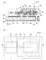
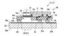
(第一実施形態)
図1は、本発明の半導体実装装置の一例を模式的に示す図であり、(a)は断面図、(b)は平面図である。図1(a)は、図1(b)のA−A間の断面図である。
この半導体実装装置1A(1)は、絶縁基板10と、前記絶縁基板10の一面10a側に配された誘電体層11と、前記誘電体層11上に配された1以上の第一端子部14a,14bと、前記1以上の第一端子部14a,14bおよび高周波信号端子14zにバンプ31を介して実装された高周波半導体30と、を少なくとも備えた半導体装置40に、パッチアンテナ20を構成するアンテナ部21を備える。(First embodiment)
FIG. 1 is a diagram schematically showing an example of a semiconductor mounting apparatus according to the present invention, where (a) is a cross-sectional view and (b) is a plan view. Fig.1 (a) is sectional drawing between AA of FIG.1 (b).
The
そして本発明の半導体実装装置1A(1)は、前記絶縁基板10の他面10b側に配されたプリント基板50と、前記プリント基板50の前記絶縁基板10と対向する面50a、または反対側の面50bに配されたアンテナ上面部22と、前記プリント基板50の前記面50aに配され、一端部が前記アンテナ上面部22と電気的に接続された伝送線路23、及び1以上の第二端子部52a,52bと、前記プリント基板50において前記アンテナ上面部22が配された面50aと反対側の面50bに配された第一接地パターン51と、を有し、前記アンテナ部21は、前記アンテナ上面部22、前記プリント基板50、及び前記第一接地パターン51により構成されるとともに、前記第一端子部14a,14bと前記第二端子部52a,52bとが電気的に接続されていることを特徴とする。 The
本発明では、アンテナ上面部22を、プリント基板50の絶縁基板10と対向する面50aまたは反対側の面50bに配することで、アンテナの放射方向を選択することができる。また、本発明の半導体実装装置1A(1)では、前記アンテナ部21は、前記アンテナ上面部22、前記プリント基板50、及び前記第一接地パターン51により構成されるとともに、前記第一端子部14a,14bと第二端子部52a,52bとが電気的に接続されているので、本発明の半導体実装装置1A(1)は、パッチアンテナ20と半導体装置40の短距離接続、低寄生インダクタンス接続を可能とし、放射効率のよいパッチアンテナ20を内蔵したものとなる。 In the present invention, the antenna
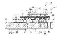
この半導体実装装置1A(1)は、半導体装置40に高周波半導体30を小型のバンプ31によりフリップチップ実装し、高周波半導体30の高周波信号端子14zとパッチアンテナ20のパッチ或いは伝送線路23とが小型のバンプ31により電気的に接続されたものである。
この半導体実装装置1A(1)では、パッチアンテナ20は、アンテナ上面部22、プリント基板50、及び第一接地パターン51により構成される。
高周波半導体30は、低雑音増幅器や電圧制御発振器、電力増幅器、発振器等のRF回路やベースバンド処理回路等のデジタル回路を備えたLSIチップであってもよい。In the
In the
The high-
前記絶縁基板10は、絶縁材又は半絶縁材からなり、例えばシリコンからなる基板が用いられる。
本発明では、MFIC(半導体装置40)を誘電体の厚みが100μm以上とされるプリント基板50と直結できるような構造とした。また、絶縁基板10に第一貫通配線17を設けることでパッチアンテナ20と半導体装置40の短距離接続を可能とした。短距離接続を実現するには、絶縁基板10は裏面研削等で薄肉化されることが望ましい。The insulating
In the present invention, the MFIC (semiconductor device 40) has a structure that can be directly connected to the printed
この半導体実装装置1A(1)では、前記誘電体層11を貫通して配されたビア16、前記絶縁基板10を貫通して配され前記ビア16と電気的に接続された第一貫通配線17、及び前記第一貫通配線17と電気的に接続されたバンプ58を介して、前記第一端子部14a,14bと第二端子部52a,52bとが電気的に接続されている。 In this
図1に示すように、半導体実装装置1A(1)において、パッチアンテナ20のパッチに対するグランドは、プリント基板50の面50bの第一接地パターン51である。
また、プリント基板50を貫通して配されたスルーホール55を介して、前記第二端子部52a,52bと前記第一接地パターン51とが、電気的に接続されている。
また、絶縁基板10の一面10aと前記誘電体層11との間に配された第二接地パターン19を、さらに備えていてもよい。これにより、伝送線路の特性インピーダンス(又は線路幅)を規定することができる。すなわち、第二接地パターン19は、絶縁基板10上の伝送線路に対するグランド(中間グランド)として機能する。As shown in FIG. 1, in the
In addition, the second
Further, a
図2に示す半導体実装装置1B(1)のように、半導体装置40の高周波信号が通過する第一貫通配線17およびバンプ31を基板外側にもってきてもよい。パッチアンテナ20と半導体装置40を最短距離で接続でき、伝送損失を低減できる。 As in the
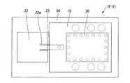
また、図3に示す半導体実装装置1D(1)のように、前記絶縁基板10の外周域において、前記第一接地パターン51の端部と前記アンテナ上面部22の端部との、面内方向の距離d1が、アンテナの動作周波数における波長λよりも大きくなされていることが好ましい。これにより有限なグランド基板が及ぼすアンテナ特性への影響を回避することができ、放射効率のよいパッチアンテナ20となる。
図4に示す半導体実装装置1E(1)は、マイクロストリップラインをベースとした機能素子18(電力合成回路、フィルタ)を用いた例である。Further, as in the
A
また、図5に示す半導体実装装置1F(1)のように、アンテナ入力のインピーダンス整合のために、アンテナ上面部22の面内においてスリット22aを形成していてもよい。
さらに、図6に示す半導体実装装置1G(1)のように、アンテナ上面部22を、多層構造とし、パッチの適当な場所で給電を行うことによりインピーダンス整合をとってもよい。Further, as in the
Further, as in the
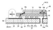
また、図7に示す半導体実装装置1H(1)のように、半導体装置40の高周波信号端子以外の端子(第一端子部14a,14b)と、プリント基板50の端子(第二端子部51a,51b)がワイヤボンド41により電気的に接続されていてもよい。この場合、半導体装置40やプリント基板50のボンディングパッドはNi/Au等の表面処理が行われることが好ましい。なお、電気的機能を有するバンプ59の他に、絶縁基板10とプリント基板50との間隔を確保するために、電気的機能を持たないバンプ57(57a、57b、57c)が配されていてもよい。 Further, as in the
(第二実施形態)
次に、本発明の半導体実装装置の第二実施形態について説明する。
なお、以下に示す説明では、上述した実施形態と異なる部分について主に説明し、第一実施形態と同様の部分については、その説明を省略する。
図8は、本実施形態に係る半導体実装装置1I(1)の一構成例を模式的に示す断面図である。
この半導体実装装置1I(1)は、前記アンテナ上面部22が、前記プリント基板50の前記面50bに配され、前記プリント基板50を貫通して配された第二貫通配線56を介して、前記アンテナ上面部22と前記伝送線路23とが電気的に接続されている。(Second embodiment)
Next, a second embodiment of the semiconductor mounting apparatus of the present invention will be described.
In the following description, parts different from the above-described embodiment will be mainly described, and description of parts similar to those in the first embodiment will be omitted.
FIG. 8 is a cross-sectional view schematically showing a configuration example of the semiconductor mounting apparatus 1I (1) according to the present embodiment.
In the semiconductor mounting apparatus 1I (1), the antenna
上述した半導体実装装置1A(1)では、プリント基板50の一面50a側にアンテナ上面部22が配されていたが、本実施形態の半導体実装装置1I(1)では、アンテナ上面部22が、プリント基板50の他面50b側に配されている。また、対向するプリント基板50の面50a側に第一接地パターン51(グランド層)が設けられている。
本発明では、アンテナ上面部22を、プリント基板50の絶縁基板10と対向する面50aまたは反対側の面50bに配することができるので、アンテナの放射方向を選択することができる。本実施形態は、プリント基板50の面50b側に電波が放射する形態としたものである。In the
In the present invention, the antenna
また、図9に示す半導体実装装置1J(1)は、プリント基板50の面50b側にアンテナ上面部22を設けるとともに、対向するプリント基板50の面50a側に第一接地パターン51(グランド層)を設け、さらに第一接地パターン51に接地電位の端子(電気的機能を有するバンプ59)を接続したものである。このような構造とすることにより装置の小型化が可能となる。 Further, in the
(第三実施形態)
次に、本発明の半導体実装装置の第三実施形態について説明する。
なお、以下に示す説明では、上述した実施形態と異なる部分について主に説明し、第一実施形態と同様の部分については、その説明を省略する。
図10は、本実施形態に係る半導体実装装置1K(1)の一構成例を模式的に示す断面図である。
この半導体実装装置1K(1)は、絶縁基板10と、前記絶縁基板10の一面10a側に配された誘電体層11と、前記誘電体層11上に配されたアンテナ上面部22と、一端部が前記アンテナ上面部22と電気的に接続された伝送線路23、及び1以上の第一端子部14a,14bと、前記1以上の第一端子部14a,14bにバンプ31を介して実装された高周波半導体30と、を少なくとも備えた半導体装置40に、パッチアンテナ20を構成するアンテナ部21を備える。(Third embodiment)
Next, a third embodiment of the semiconductor mounting apparatus of the present invention will be described.
In the following description, parts different from the above-described embodiment will be mainly described, and description of parts similar to those in the first embodiment will be omitted.
FIG. 10 is a cross-sectional view schematically showing a configuration example of the
The
そして、この半導体実装装置1K(1)は、絶縁基板10の他面10b側に配されたプリント基板50と、該プリント基板50の絶縁基板10と対向する面50a、または反対側の面50bに配された第一接地パターン51と、プリント基板50の前記面50aに配され、第一端子部14a,14bと電気的に接続された第二端子部52a,52bと、を有する。前記アンテナ部21は、アンテナ上面部22、誘電体層11、絶縁基板10、第一接地パターン51、及びプリント基板50により構成される。また、前記アンテナ部21は、アンテナ上面部22に対応する部位において、絶縁基板10の他面10b側が薄板化されていることを特徴とする。 The
本実施形態の半導体実装装置1K(1)は、誘電体層11の積層構造内にアンテナパッチを設け、その下部の絶縁基板10を掘り込んだ構造としたものである。アンテナ上面部22に対応する部位において、絶縁基板10の他面10b側が薄板化されていることで、絶縁基板10とプリント基板50との間に、薄板化されたことによる凹部10cの深さ分の空気層を形成することができ、空気が誘電体層となり、誘電体損失が低減できる。 The
なお、図10に示す半導体実装装置1K(1)では、アンテナ上面部22に対応する部位の絶縁基板10のみを薄板化しているが、後掲する半導体実装装置1L(1)(プリント基板50の前記面50a側に第一接地パターン51が配されたもの)と比較すると、低周波側に対応できる。何故ならば、半導体実装装置1L(1)に比べて半導体実装装置1K(1)は、アンテナ上面部22と第一接地パターン(GND)51との間が、スルーホール55の厚み分だけ大きいからである。 In the
また、図10に示す半導体実装装置1K(1)では、第一接地パターン51がプリント基板50の前記面50b側に配されていたが、図11に示す半導体実装装置1L(1)のように、第一接地パターン51をプリント基板50の前記面50a側に配してもよい。 Further, in the
また、図12に示す半導体実装装置1M(1)は、アンテナ上面部22に対応する部位の絶縁基板10とプリント基板50の双方を薄板化したものである。この構成によれば、プリント基板50の誘電体が純粋な空気に置換されたことになるため、半導体実装装置1K(1)に比べて半導体実装装置1M(1)は、誘電体損失を減らすことができる。ゆえに、上記効果をより良好に得ることが可能となり、更なるアンテナの放射効率の向上が期待できる。 Further, the
なお、図12では、アンテナ上面部22に対応する部位の絶縁基板10とプリント基板50の双方を薄板化したもの、について詳述したが、プリント基板50のみ薄板化した構成(不図示)としてもよい。何故ならば、プリント基板50のみ薄板化した構成においても、プリント基板50の誘電体が純粋な空気に置換されることによる、上記の作用・効果は確実に得られるからである。 In FIG. 12, the insulating
(第四実施形態)
次に、本発明の半導体実装装置の第四実施形態について説明する。
なお、以下に示す説明では、上述した実施形態と異なる部分について主に説明し、第一実施形態と同様の部分については、その説明を省略する。
図13は、本実施形態に係る半導体実装装置1N(1)の一構成例を模式的に示す断面図である。
半導体実装装置1N(1)は、絶縁基板10と、前記絶縁基板10の一面10a側に配された誘電体層11と、前記誘電体層11上に配された伝送線路23及び1以上の第一端子部14a,14bと、前記1以上の第一端子部14a,14bにバンプ31を介して実装された高周波半導体30と、を少なくとも備えた半導体装置40に、パッチアンテナ20を構成するアンテナ部21を備える。(Fourth embodiment)
Next, a fourth embodiment of the semiconductor mounting apparatus of the present invention will be described.
In the following description, parts different from the above-described embodiment will be mainly described, and description of parts similar to those in the first embodiment will be omitted.
FIG. 13 is a cross-sectional view schematically showing a configuration example of the
The
そして、この半導体実装装置は、前記アンテナ部21は、ガラス基板60と、該ガラス基板上に配されたアンテナ上面部22とを有し、端子部を介して前記誘電体層11上に実装されるとともに、前記ガラス基板60を貫通して配された第三貫通配線61を通じて、前記アンテナ上面部22と前記伝送線路23とが電気的に接続されていること、を特徴とする。 In the semiconductor mounting apparatus, the
本実施形態の半導体実装装置1N(1)は、ガラス基板60上にアンテナ上面部22を配し、ガラスをパッチアンテナ20の誘電体としたものである。これにより、樹脂層からなる誘電体層11では実現不可能な誘電体厚みを確保し、放射効率を改善することが可能である。特にミリ波帯の使用において、パッチアンテナ20の実用化に十分な誘電体厚みを確保することができる。
また、半導体実装装置1N(1)は、絶縁基板10の一面10a側に配された内層GNDプレーン56を備え、第四貫通配線62を通じて、絶縁基板10の他面10b側に配されたバンプ59と電気的に接続されている。なお、内層GNDプレーン56は、アンテナ上面部22および伝送線路23と重なる位置に配されている。In the
Further, the
以上、本発明の半導体実装装置について説明してきたが、本発明は上述した例に限定されるものではなく、発明の趣旨を逸脱しない範囲で適宜変更可能である。 Although the semiconductor mounting apparatus of the present invention has been described above, the present invention is not limited to the above-described example, and can be appropriately changed without departing from the spirit of the invention.
本発明は、パッチアンテナが内蔵された半導体実装装置に広く適用可能である。 The present invention can be widely applied to semiconductor mounting apparatuses having a built-in patch antenna.
1A〜1N(1) 半導体実装装置、10 絶縁基板、11 誘電体層、14a,14b 第一端子部、19 第二接地パターン、20 パッチアンテナ、21 アンテナ部、22 アンテナ上面部、23 伝送線路、30 高周波半導体、31 バンプ、40 半導体装置、50 プリント基板、51 第一接地パターン、52a,52b 第二端子部。 1A to 1N (1) Semiconductor mounting device, 10 insulating substrate, 11 dielectric layer, 14a, 14b first terminal portion, 19 second ground pattern, 20 patch antenna, 21 antenna portion, 22 antenna upper surface portion, 23 transmission line, 30 high-frequency semiconductor, 31 bump, 40 semiconductor device, 50 printed circuit board, 51 first ground pattern, 52a, 52b second terminal portion.
Claims (12)
Translated fromJapanese前記誘電体層上に配された1以上の第一端子部と、
前記1以上の第一端子部にバンプを介して実装された高周波半導体と、を少なくとも備えた半導体装置に、パッチアンテナを構成するアンテナ部を備えた半導体実装装置であって、
前記絶縁基板の他面側に配されたプリント基板と、
前記プリント基板の前記絶縁基板と対向する面a、または反対側の面bに配されたアンテナ上面部と、
前記プリント基板の前記面aに配され、一端部が前記アンテナ上面部と電気的に接続された伝送線路、及び1以上の第二端子部と、
前記プリント基板において前記アンテナ上面部が配された面と反対側の面に配された第一接地パターンと、を有し、
前記アンテナ部は、前記アンテナ上面部、前記プリント基板、及び前記第一接地パターンにより構成されるとともに、
前記第一端子部と前記第二端子部とが電気的に接続されていることを特徴とする半導体実装装置。An insulating substrate; and a dielectric layer disposed on one side of the insulating substrate;
One or more first terminal portions disposed on the dielectric layer;
A semiconductor device provided with an antenna part constituting a patch antenna on a semiconductor device comprising at least a high-frequency semiconductor mounted on the one or more first terminal parts via bumps,
A printed circuit board disposed on the other surface side of the insulating substrate;
An antenna upper surface portion disposed on a surface a facing the insulating substrate of the printed circuit board, or a surface b on the opposite side;
A transmission line disposed on the surface a of the printed circuit board and having one end electrically connected to the antenna upper surface, and one or more second terminal portions;
A first grounding pattern disposed on a surface opposite to the surface on which the antenna upper surface portion is disposed on the printed circuit board;
The antenna portion is constituted by the antenna upper surface portion, the printed circuit board, and the first ground pattern,
The semiconductor mounting apparatus, wherein the first terminal portion and the second terminal portion are electrically connected.
前記絶縁基板を貫通して配され前記ビアと電気的に接続された第一貫通配線、及び前記第一貫通配線と電気的に接続されたバンプを介して、
前記第一端子部と第二端子部とが電気的に接続されていることを特徴とする請求項1に記載の半導体実装装置。Vias disposed through the dielectric layer;
Through the first through wiring that is arranged through the insulating substrate and electrically connected to the via, and the bump that is electrically connected to the first through wiring,
The semiconductor mounting apparatus according to claim 1, wherein the first terminal portion and the second terminal portion are electrically connected.
前記プリント基板を貫通して配された第二貫通配線を介して、前記アンテナ上面部と前記伝送線路とが電気的に接続されていること、を特徴とする請求項1に記載の半導体実装装置。The antenna upper surface portion is disposed on the surface b of the printed circuit board,
2. The semiconductor mounting apparatus according to claim 1, wherein the upper surface portion of the antenna and the transmission line are electrically connected via a second through wiring arranged to penetrate the printed circuit board. .
前記誘電体層上に配されたアンテナ上面部と、
一端部が前記アンテナ上面部と電気的に接続された伝送線路、及び1以上の第一端子部と、
前記1以上の第一端子部にバンプを介して実装された高周波半導体と、を少なくとも備えた半導体装置に、パッチアンテナを構成するアンテナ部を備えた半導体実装装置であって、
前記絶縁基板の他面側に配されたプリント基板と、該プリント基板の前記絶縁基板と対向する面a、または反対側の面bに配された第一接地パターンと、
前記該プリント基板の前記面aに配され、前記第一端子部と電気的に接続された第二端子部と、を有し、
前記アンテナ部は、前記アンテナ上面部、前記誘電体層、前記絶縁基板、及び前記第一接地パターンにより構成されるとともに、
前記アンテナ上面部に対応する部位において、前記絶縁基板の他面側が薄板化されていることを特徴とする半導体実装装置。An insulating substrate; and a dielectric layer disposed on one side of the insulating substrate;
An antenna upper surface portion disposed on the dielectric layer;
A transmission line having one end portion electrically connected to the antenna upper surface portion, and one or more first terminal portions;
A semiconductor device provided with an antenna part constituting a patch antenna on a semiconductor device comprising at least a high-frequency semiconductor mounted on the one or more first terminal parts via bumps,
A printed circuit board disposed on the other surface side of the insulating substrate, a surface a facing the insulating substrate of the printed circuit board, or a first ground pattern disposed on the opposite surface b;
A second terminal portion disposed on the surface a of the printed circuit board and electrically connected to the first terminal portion;
The antenna portion is constituted by the antenna upper surface portion, the dielectric layer, the insulating substrate, and the first ground pattern,
A semiconductor mounting apparatus, wherein the other surface side of the insulating substrate is thinned at a portion corresponding to the antenna upper surface.
前記誘電体層上に配された伝送線路及び1以上の第一端子部と、
前記1以上の第一端子部にバンプを介して実装された高周波半導体と、を少なくとも備えた半導体装置に、パッチアンテナを構成するアンテナ部を備えた半導体実装装置であって、
前記アンテナ部は、ガラス基板と、該ガラス基板上に配されたアンテナ上面部とを有し、端子部を介して前記誘電体層上に実装されるとともに、
前記ガラス基板を貫通して配された第三貫通配線を通じて、前記アンテナ上面部と前記伝送線路とが電気的に接続されていること、を特徴とする半導体実装装置。An insulating substrate; and a dielectric layer disposed on one side of the insulating substrate;
A transmission line and one or more first terminal portions disposed on the dielectric layer;
A semiconductor device provided with an antenna part constituting a patch antenna on a semiconductor device comprising at least a high-frequency semiconductor mounted on the one or more first terminal parts via bumps,
The antenna part has a glass substrate and an antenna upper surface part arranged on the glass substrate, and is mounted on the dielectric layer via a terminal part,
The semiconductor mounting apparatus, wherein the antenna upper surface portion and the transmission line are electrically connected through a third through wiring arranged through the glass substrate.
Priority Applications (1)
| Application Number | Priority Date | Filing Date | Title |
|---|---|---|---|
| JP2010152326AJP2012015909A (en) | 2010-07-02 | 2010-07-02 | Semiconductor mounting device |
Applications Claiming Priority (1)
| Application Number | Priority Date | Filing Date | Title |
|---|---|---|---|
| JP2010152326AJP2012015909A (en) | 2010-07-02 | 2010-07-02 | Semiconductor mounting device |
Publications (1)
| Publication Number | Publication Date |
|---|---|
| JP2012015909Atrue JP2012015909A (en) | 2012-01-19 |
Family
ID=45601786
Family Applications (1)
| Application Number | Title | Priority Date | Filing Date |
|---|---|---|---|
| JP2010152326APendingJP2012015909A (en) | 2010-07-02 | 2010-07-02 | Semiconductor mounting device |
Country Status (1)
| Country | Link |
|---|---|
| JP (1) | JP2012015909A (en) |
Cited By (7)
| Publication number | Priority date | Publication date | Assignee | Title |
|---|---|---|---|---|
| CN103887186A (en)* | 2012-12-20 | 2014-06-25 | 英特尔公司 | Package structure including discrete antenna assembled on device |
| JP2015530055A (en)* | 2012-09-11 | 2015-10-08 | アルカテル−ルーセント | Integrated antenna with high radiation efficiency |
| US9437535B2 (en) | 2013-01-29 | 2016-09-06 | Panasonic Intellectual Property Management Co., Ltd. | Wireless module and production method for wireless module |
| WO2017111767A1 (en) | 2015-12-22 | 2017-06-29 | Intel Corporation | Microelectronic devices designed with integrated antennas on a substrate |
| WO2018194546A1 (en)* | 2017-04-17 | 2018-10-25 | Hewlett-Packard Development Company, L.P. | Antenna elements |
| JP2019097026A (en)* | 2017-11-22 | 2019-06-20 | 株式会社村田製作所 | Radio communication module |
| US11363718B2 (en)* | 2019-10-30 | 2022-06-14 | Samsung Electronics Co., Ltd | Oscillator structure and electronic device including the same |
- 2010
- 2010-07-02JPJP2010152326Apatent/JP2012015909A/enactivePending
Cited By (14)
| Publication number | Priority date | Publication date | Assignee | Title |
|---|---|---|---|---|
| JP2015530055A (en)* | 2012-09-11 | 2015-10-08 | アルカテル−ルーセント | Integrated antenna with high radiation efficiency |
| CN103887186A (en)* | 2012-12-20 | 2014-06-25 | 英特尔公司 | Package structure including discrete antenna assembled on device |
| JP2014123945A (en)* | 2012-12-20 | 2014-07-03 | Intel Corp | Package structures including discrete antennas installed on device |
| US9166284B2 (en) | 2012-12-20 | 2015-10-20 | Intel Corporation | Package structures including discrete antennas assembled on a device |
| US9419339B2 (en) | 2012-12-20 | 2016-08-16 | Intel Corporation | Package structures including discrete antennas assembled on a device |
| US9437535B2 (en) | 2013-01-29 | 2016-09-06 | Panasonic Intellectual Property Management Co., Ltd. | Wireless module and production method for wireless module |
| WO2017111767A1 (en) | 2015-12-22 | 2017-06-29 | Intel Corporation | Microelectronic devices designed with integrated antennas on a substrate |
| US20180332151A1 (en)* | 2015-12-22 | 2018-11-15 | Intel Corporation | Microelectronic devices designed with integrated antennas on a substrate |
| US10887439B2 (en) | 2015-12-22 | 2021-01-05 | Intel Corporation | Microelectronic devices designed with integrated antennas on a substrate |
| EP3764466A1 (en)* | 2015-12-22 | 2021-01-13 | INTEL Corporation | Microelectronic devices designed with integrated antennas on a substrate |
| WO2018194546A1 (en)* | 2017-04-17 | 2018-10-25 | Hewlett-Packard Development Company, L.P. | Antenna elements |
| US10985452B2 (en) | 2017-04-17 | 2021-04-20 | Hewlett-Packard Development Company, L.P. | Antenna elements |
| JP2019097026A (en)* | 2017-11-22 | 2019-06-20 | 株式会社村田製作所 | Radio communication module |
| US11363718B2 (en)* | 2019-10-30 | 2022-06-14 | Samsung Electronics Co., Ltd | Oscillator structure and electronic device including the same |
Similar Documents
| Publication | Publication Date | Title |
|---|---|---|
| KR100634947B1 (en) | High-frequency device | |
| JP5763704B2 (en) | Semiconductor integrated circuit | |
| US10950569B2 (en) | High frequency module and communication device | |
| JP5239309B2 (en) | Semiconductor device | |
| JP3378435B2 (en) | Ultra-high frequency band wireless communication device | |
| JP5199307B2 (en) | Semiconductor device | |
| JP2012015909A (en) | Semiconductor mounting device | |
| WO2019181589A1 (en) | High-frequency module and communication device | |
| JP2790033B2 (en) | Semiconductor device | |
| JP2020027973A (en) | High frequency module and communication device | |
| WO2021044691A1 (en) | High frequency module and communication device | |
| US11716103B2 (en) | Radio-frequency module and communication device | |
| US12323171B2 (en) | Radio frequency module and communication device | |
| WO2021039076A1 (en) | High-frequency module and communication device | |
| JP2011097526A (en) | Millimeter wave radio device | |
| JP5412372B2 (en) | Semiconductor mounting equipment | |
| US8288845B2 (en) | Package including proximately-positioned lead frame | |
| JP2020088468A (en) | Amplifier and amplifier | |
| WO2011104774A1 (en) | Semiconductor device | |
| WO2022186132A1 (en) | High frequency module and communication device | |
| JP2010245819A (en) | Amplifier circuit | |
| US12354979B2 (en) | High frequency device | |
| JP2025077661A (en) | High-frequency circuit components | |
| WO2021241064A1 (en) | High-frequency module and communication device | |
| JP2012044063A (en) | Semiconductor module, communication module, and surface-mounted component |