JP2012010533A - Power transmission system, and power supply device and portable apparatus therefor - Google Patents
Power transmission system, and power supply device and portable apparatus thereforDownload PDFInfo
- Publication number
- JP2012010533A JP2012010533AJP2010145731AJP2010145731AJP2012010533AJP 2012010533 AJP2012010533 AJP 2012010533AJP 2010145731 AJP2010145731 AJP 2010145731AJP 2010145731 AJP2010145731 AJP 2010145731AJP 2012010533 AJP2012010533 AJP 2012010533A
- Authority
- JP
- Japan
- Prior art keywords
- coil
- power
- spiral inductor
- inner diameter
- transmission system
- Prior art date
- Legal status (The legal status is an assumption and is not a legal conclusion. Google has not performed a legal analysis and makes no representation as to the accuracy of the status listed.)
- Pending
Links
- 230000005540biological transmissionEffects0.000titleclaimsabstractdescription36
- 239000004020conductorSubstances0.000claimsabstractdescription45
- 230000004907fluxEffects0.000claimsdescription14
- 239000000126substanceSubstances0.000abstract1
- 230000008878couplingEffects0.000description9
- 238000010168coupling processMethods0.000description9
- 238000005859coupling reactionMethods0.000description9
- 238000010586diagramMethods0.000description7
- 239000000696magnetic materialSubstances0.000description6
- 229910000859α-FeInorganic materials0.000description6
- 230000007423decreaseEffects0.000description5
- 239000011347resinSubstances0.000description5
- 229920005989resinPolymers0.000description5
- 230000006866deteriorationEffects0.000description4
- 230000014759maintenance of locationEffects0.000description3
- WABPQHHGFIMREM-UHFFFAOYSA-Nlead(0)Chemical compound[Pb]WABPQHHGFIMREM-UHFFFAOYSA-N0.000description2
- 230000035699permeabilityEffects0.000description2
- RYGMFSIKBFXOCR-UHFFFAOYSA-NCopperChemical compound[Cu]RYGMFSIKBFXOCR-UHFFFAOYSA-N0.000description1
- 229910007565Zn—CuInorganic materials0.000description1
- 229910000828alnicoInorganic materials0.000description1
- 239000003990capacitorSubstances0.000description1
- 239000010949copperSubstances0.000description1
- 230000020169heat generationEffects0.000description1
- 238000004898kneadingMethods0.000description1
- 239000000463materialSubstances0.000description1
- 229910001172neodymium magnetInorganic materials0.000description1
- 239000000843powderSubstances0.000description1
Images


Classifications
- Y—GENERAL TAGGING OF NEW TECHNOLOGICAL DEVELOPMENTS; GENERAL TAGGING OF CROSS-SECTIONAL TECHNOLOGIES SPANNING OVER SEVERAL SECTIONS OF THE IPC; TECHNICAL SUBJECTS COVERED BY FORMER USPC CROSS-REFERENCE ART COLLECTIONS [XRACs] AND DIGESTS
- Y02—TECHNOLOGIES OR APPLICATIONS FOR MITIGATION OR ADAPTATION AGAINST CLIMATE CHANGE
- Y02E—REDUCTION OF GREENHOUSE GAS [GHG] EMISSIONS, RELATED TO ENERGY GENERATION, TRANSMISSION OR DISTRIBUTION
- Y02E60/00—Enabling technologies; Technologies with a potential or indirect contribution to GHG emissions mitigation
- Y02E60/10—Energy storage using batteries
Landscapes
- Telephone Set Structure (AREA)
- Charge And Discharge Circuits For Batteries Or The Like (AREA)
- Secondary Cells (AREA)
- Battery Mounting, Suspending (AREA)
Abstract
Description
Translated fromJapanese本発明は、物理的に接続することなく電力を伝送する電力伝送システム、該電力伝送システムの給電装置及び携帯機器に関する。 The present invention relates to a power transmission system that transmits power without being physically connected, a power supply apparatus for the power transmission system, and a portable device.
近年、非接触で電力を伝送して充電する通信機等の電子機器が開発されている。電子機器において非接触で電力を伝送するためには、電力の給電側の電子機器と、電力の受電側の電子機器との双方に非接触型電力伝送用のコイルを設ける必要がある。 2. Description of the Related Art In recent years, electronic devices such as communication devices that are charged by transmitting power without contact have been developed. In order to transmit electric power in an electronic device in a non-contact manner, it is necessary to provide a coil for non-contact power transmission in both the electronic device on the power supply side and the electronic device on the power reception side.
また、電力の給電側のコイルと、電力の受電側のコイルとで、位置合わせを行わないと、効果的に電力を伝送することができない。そこで、例えば特許文献1では、電力の給電側の電子機器、受電側の電子機器の双方のコイルの中心部分に磁石を配置し、両磁石間の引き合う力を利用して電力の給電側のコイルと、電力の受電側のコイルとで、位置合わせを行っていた。 Moreover, unless alignment is performed between the coil on the power feeding side and the coil on the power receiving side, the power cannot be effectively transmitted. Therefore, in Patent Document 1, for example, a magnet is arranged in the center of both coils of the power supply side electronic device and the power reception side electronic device, and the power supply side coil is utilized by using the attractive force between the two magnets. And positioning with the coil on the power receiving side.
しかし、電力の給電側の電子機器、受電側の電子機器の双方のコイルの中心部分に磁石を配置するためには、コイル自体をある程度の大きさにする必要があり、小型化することが困難になるという問題点があった。特に受電側の電子機器、例えば携帯電話機に組み込む場合、コイルが一定以上の大きさを要することから、裏蓋と一体化させる案が有力であるが、電池近傍における発熱の問題等があり、コイルの大きさが携帯電話機の設計上の大きな制約条件となっている。 However, in order to place a magnet in the central part of the coil of both the electronic device on the power supply side and the electronic device on the power reception side, it is necessary to make the coil itself a certain size, and it is difficult to reduce the size. There was a problem of becoming. In particular, when it is incorporated into an electronic device on the power receiving side, for example, a mobile phone, the coil needs to be larger than a certain size. Therefore, it is a good idea to integrate it with the back cover, but there is a problem of heat generation near the battery. This is a major constraint on the design of mobile phones.
本発明は、上記事情に鑑みてなされたものであり、電力を伝送する能力を維持しつつ、受電側のコイルを小型化することができる電力伝送システム、該電力伝送システムの給電装置及び携帯機器を提供することを目的とする。 The present invention has been made in view of the above circumstances, and can maintain a capability of transmitting power while reducing the size of a coil on a power receiving side, a power feeding device of the power transmission system, and a portable device The purpose is to provide.
上記目的を達成するために第1発明に係る電力伝送システムは、電力を供給する給電装置と、電力の供給を受ける受電装置とを備える電力伝送システムにおいて、前記給電装置は、平板状の第一のコイルと、該第一のコイルの内径部分に配置された磁石とを備え、前記受電装置は、前記第一のコイルの内径と略同じ又は該内径より小さい外径の第二のコイルを備え、該第二のコイルは、軟磁性体層とコイル導体とで構成されたスパイラルインダクタである。 In order to achieve the above object, a power transmission system according to a first aspect of the present invention is a power transmission system including a power supply device that supplies power and a power reception device that receives the supply of power. And a magnet disposed on an inner diameter portion of the first coil, and the power receiving device includes a second coil having an outer diameter substantially the same as or smaller than the inner diameter of the first coil. The second coil is a spiral inductor composed of a soft magnetic layer and a coil conductor.
また、第2発明に係る電力伝送システムは、第1発明において、前記スパイラルインダクタは、前記給電装置に対向している面側の漏れ磁束が、対向している該面側とは反対の面側の漏れ磁束より大きくなるようにしてある。 The power transmission system according to a second aspect of the present invention is the power transmission system according to the first aspect, wherein the spiral inductor has a surface on the opposite side to the surface facing the leakage magnetic flux on the surface facing the power feeding device. It is designed to be larger than the leakage magnetic flux.
また、第3発明に係る電力伝送システムは、第1又は第2発明において、前記スパイラルインダクタは、前記給電装置に対向している面側とは反対の面側に、回路基板を実装するようにしてある。 The power transmission system according to a third aspect of the present invention is the power transmission system according to the first or second aspect, wherein the spiral inductor has a circuit board mounted on a surface opposite to a surface facing the power feeding device. It is.
上記目的を達成するために第4発明に係る給電装置は、軟磁性体層とコイル導体とで構成されたスパイラルインダクタを備える受電装置に対して、電力を供給する給電装置であって、平板状のコイルと、該コイルの内径部分に配置された磁石とを備え、前記コイルの内径は、前記受電装置の前記コイル導体の外径と略同じ又は該外径より大きい。 In order to achieve the above object, a power feeding device according to a fourth aspect of the present invention is a power feeding device that supplies power to a power receiving device including a spiral inductor composed of a soft magnetic layer and a coil conductor, and has a flat plate shape. And a magnet disposed on an inner diameter portion of the coil, and the inner diameter of the coil is substantially the same as or larger than the outer diameter of the coil conductor of the power receiving device.
上記目的を達成するために第5発明に係る携帯機器は、平板状のコイルと、該コイルの内径部分に配置された磁石とを備える給電装置から電力の供給を受ける携帯機器であって、軟磁性体層とコイル導体とで構成されたスパイラルインダクタと、該スパイラルインダクタと離隔して配置され、二次電池を収納している電池収納部とを備え、前記コイル導体の外径は、前記給電装置の前記コイルの内径と略同じ又は該内径より小さい。 In order to achieve the above object, a portable device according to a fifth aspect of the present invention is a portable device that is supplied with electric power from a power feeding device that includes a flat coil and a magnet disposed on an inner diameter portion of the coil, and is a soft device. A spiral inductor composed of a magnetic material layer and a coil conductor; and a battery storage part that is spaced apart from the spiral inductor and stores a secondary battery. The outer diameter of the coil conductor is the power supply It is substantially the same as or smaller than the inner diameter of the coil of the apparatus.
第1発明では、給電装置が、平板状の第一のコイルと、該第一のコイルの内径部分に配置された磁石とを備え、受電装置が、第一のコイルの内径と略同じ又は該内径より小さい外径の第二のコイルを備えるので、給電装置の第一のコイルと受電装置の第二のコイルとの結合係数は低下するが、第一のコイルの内径部分に配置された磁石により、エネルギーの保持と損失との関係を示す指標であるQ値を高くすることができるため、電力を伝送する能力を維持することができる。また、第一のコイルの内径部分に配置された磁石と受電装置の軟磁性体層との間の引き合う力を利用して、給電装置の第一のコイルと受電装置の第二のコイルとの位置合わせを容易に行うことができる。さらに、受電装置の第二のコイルをスパイラルインダクタとすることで、受電側(受電装置)のコイル(第二のコイル)を小型化することができる。 In the first invention, the power supply device includes a flat plate-like first coil and a magnet disposed on an inner diameter portion of the first coil, and the power receiving device is substantially the same as the inner diameter of the first coil, or the Since the second coil having the outer diameter smaller than the inner diameter is provided, the coupling coefficient between the first coil of the power feeding device and the second coil of the power receiving device is reduced, but the magnet disposed in the inner diameter portion of the first coil Thus, the Q value, which is an index indicating the relationship between energy retention and loss, can be increased, so that the ability to transmit power can be maintained. Further, by utilizing the attractive force between the magnet disposed on the inner diameter portion of the first coil and the soft magnetic layer of the power receiving device, the first coil of the power feeding device and the second coil of the power receiving device Positioning can be performed easily. Furthermore, the coil (second coil) on the power receiving side (power receiving device) can be reduced in size by using the second coil of the power receiving device as a spiral inductor.
第2発明では、スパイラルインダクタは、給電装置に対向している面側の漏れ磁束が、対向している該面側とは反対の面側の漏れ磁束よりも大きくなるようにしてあるので、給電装置に対向している面側とは反対の面側からの磁束の漏れを抑えて、給電装置の第一のコイルとの電磁結合に利用される磁束を大きくすることができ、電力を伝送する能力を維持することができる。 In the second invention, the spiral inductor is configured such that the leakage magnetic flux on the surface facing the power feeding device is larger than the leakage magnetic flux on the surface opposite to the facing surface. By suppressing leakage of magnetic flux from the surface opposite to the surface facing the device, the magnetic flux used for electromagnetic coupling with the first coil of the power supply device can be increased, and power is transmitted. Ability can be maintained.
第3発明では、スパイラルインダクタは、給電装置に対向している面とは反対の面側に、回路基板を実装するようにしてあるので、スパイラルインダクタと回路基板とで構成されるコイルモジュールを小型化して、受電装置を小型化することができる。 In the third aspect of the invention, the spiral inductor is configured such that the circuit board is mounted on the surface opposite to the surface facing the power feeding device, so that the coil module composed of the spiral inductor and the circuit board is reduced in size. Thus, the power receiving device can be reduced in size.
第4発明では、軟磁性体層とコイル導体とで構成されたスパイラルインダクタを備える受電装置に対して、電力を供給する給電装置であって、平板状のコイルと、該コイルの内径部分に配置された磁石とを備え、コイルの内径は、受電装置のコイル導体の外径と略同じ又は該外径より大きいので、給電装置のコイルと受電装置のコイル導体との結合係数は低下するが、コイルの内径部分に配置された磁石により、Q値を高くすることができるため、電力を伝送する能力を維持することができる。また、コイルの内径部分に配置された磁石と受電装置の軟磁性体層との間の引き合う力を利用して、給電装置のコイルと受電装置のコイル導体との位置合わせを容易に行うことができる。 According to a fourth aspect of the present invention, there is provided a power feeding device that supplies power to a power receiving device including a spiral inductor composed of a soft magnetic material layer and a coil conductor, and is arranged on a flat coil and an inner diameter portion of the coil The inner diameter of the coil is substantially the same as or larger than the outer diameter of the coil conductor of the power receiving device, so that the coupling coefficient between the coil of the power feeding device and the coil conductor of the power receiving device decreases. Since the Q value can be increased by the magnet disposed in the inner diameter portion of the coil, the ability to transmit electric power can be maintained. Further, it is possible to easily align the coil of the power feeding device and the coil conductor of the power receiving device by using the attractive force between the magnet disposed on the inner diameter portion of the coil and the soft magnetic layer of the power receiving device. it can.
第5発明では、平板状のコイルと、該コイルの内径部分に配置された磁石とを備える給電装置から電力の供給を受ける携帯機器であって、軟磁性体層とコイル導体とで構成されたスパイラルインダクタと、該スパイラルインダクタと離隔して配置され、二次電池を収納している電池収納部とを備えるので、給電装置から電力の供給を受けてスパイラルインダクタが発熱しても電池収納部に熱が伝わりにくく、二次電池の劣化を抑えることができる。また、スパイラルインダクタのコイル導体の外径は、給電装置のコイルの内径と略同じ又は該内径より小さいので、携帯機器を小型化することができる。さらに、給電装置の磁石とスパイラルインダクタの軟磁性体層との間の引き合う力を利用して、給電装置のコイルとスパイラルインダクタのコイル導体との位置合わせを容易に行うことができる。 According to a fifth aspect of the present invention, there is provided a portable device that is supplied with electric power from a power supply device that includes a flat coil and a magnet disposed on an inner diameter portion of the coil, and includes a soft magnetic layer and a coil conductor. Since it includes a spiral inductor and a battery storage unit that is spaced apart from the spiral inductor and stores a secondary battery, even if the spiral inductor generates heat when receiving power from the power supply device, the battery storage unit It is difficult for heat to be transmitted and deterioration of the secondary battery can be suppressed. Further, since the outer diameter of the coil conductor of the spiral inductor is substantially the same as or smaller than the inner diameter of the coil of the power feeding device, the portable device can be reduced in size. Furthermore, it is possible to easily align the coil of the power supply device and the coil conductor of the spiral inductor using the attractive force between the magnet of the power supply device and the soft magnetic layer of the spiral inductor.
本発明に係る電力伝送システムでは、給電装置が、平板状の第一のコイルと、該第一のコイルの内径部分に配置された磁石とを備え、受電装置が、第一のコイルの内径と略同じ又は該内径より小さい外径の第二のコイルを備えるので、給電装置の第一のコイルと受電装置の第二のコイルとの結合係数は低下するが、第一のコイルの内径部分に配置された磁石により、エネルギーの保持と損失との関係を示す指標であるQ値を高くすることができるため、電力を伝送する能力を維持することができる。また、第一のコイルの内径部分に配置された磁石と受電装置の軟磁性体層との間の引き合う力を利用して、給電装置の第一のコイルと受電装置の第二のコイルとの位置合わせを容易に行うことができる。さらに、受電装置の第二のコイルをスパイラルインダクタとすることで、受電側(受電装置)のコイル(第二のコイル)を小型化することができる。 In the power transmission system according to the present invention, the power feeding device includes a flat plate-shaped first coil and a magnet disposed on an inner diameter portion of the first coil, and the power receiving device has an inner diameter of the first coil. Since a second coil having an outer diameter that is substantially the same or smaller than the inner diameter is provided, the coupling coefficient between the first coil of the power feeding device and the second coil of the power receiving device decreases, but the inner diameter portion of the first coil Since the arranged magnets can increase the Q value, which is an index indicating the relationship between energy retention and loss, the ability to transmit power can be maintained. Further, by utilizing the attractive force between the magnet disposed on the inner diameter portion of the first coil and the soft magnetic layer of the power receiving device, the first coil of the power feeding device and the second coil of the power receiving device Positioning can be performed easily. Furthermore, the coil (second coil) on the power receiving side (power receiving device) can be reduced in size by using the second coil of the power receiving device as a spiral inductor.
また、本発明に係る給電装置は、軟磁性体層とコイル導体とで構成されたスパイラルインダクタを備える受電装置に対して、電力を供給する給電装置であって、平板状のコイルと、該コイルの内径部分に配置された磁石とを備え、コイルの内径は、受電装置のコイル導体の外径と略同じ又は該外径より大きいので、給電装置のコイルと受電装置のコイル導体との結合係数は低下するが、コイルの内径部分に配置された磁石により、Q値を高くすることができるため、電力を伝送する能力を維持することができる。 A power supply device according to the present invention is a power supply device that supplies power to a power reception device including a spiral inductor composed of a soft magnetic material layer and a coil conductor, and includes a flat coil and the coil And the inner diameter of the coil is substantially the same as or larger than the outer diameter of the coil conductor of the power receiving device, so that the coupling coefficient between the coil of the power feeding device and the coil conductor of the power receiving device However, since the Q value can be increased by the magnet disposed in the inner diameter portion of the coil, the ability to transmit electric power can be maintained.
さらに、本発明に係る携帯機器は、平板状のコイルと、該コイルの内径部分に配置された磁石とを備える給電装置から電力の供給を受ける携帯機器であって、軟磁性体層とコイル導体とで構成されたスパイラルインダクタと、該スパイラルインダクタと離隔して配置され、二次電池を収納している電池収納部とを備えるので、給電装置から電力の供給を受けてスパイラルインダクタが発熱しても電池収納部に熱が伝わりにくく、二次電池の劣化を抑えることができる。 Furthermore, a portable device according to the present invention is a portable device that is supplied with electric power from a power supply device that includes a flat coil and a magnet disposed on an inner diameter portion of the coil, and includes a soft magnetic layer and a coil conductor. And a battery storage part that is spaced apart from the spiral inductor and stores the secondary battery, the spiral inductor generates heat upon receiving power supply from the power supply device. However, it is difficult for heat to be transmitted to the battery housing, and the deterioration of the secondary battery can be suppressed.
以下、本発明の実施の形態における電力伝送システム、該電力伝送システムの給電装置及び携帯機器について、図面を用いて具体的に説明する。以下の実施の形態は、特許請求の範囲に記載された発明を限定するものではなく、実施の形態の中で説明されている特徴的事項の組み合わせの全てが解決手段の必須事項であるとは限らないことは言うまでもない。 Hereinafter, a power transmission system, a power supply device of the power transmission system, and a portable device according to an embodiment of the present invention will be specifically described with reference to the drawings. The following embodiments do not limit the invention described in the claims, and all combinations of characteristic items described in the embodiments are essential to the solution. It goes without saying that it is not limited.
なお、本発明の実施の形態に係る電力伝送システムの携帯機器には、例えばミュージックプレイヤー、携帯電話機、キーレスシステムの携帯機等が含まれるが、以下の説明では、携帯機器が携帯電話機である場合について説明する。 The portable device of the power transmission system according to the embodiment of the present invention includes, for example, a music player, a portable phone, a portable device of a keyless system, etc., but in the following description, the portable device is a portable phone. Will be described.
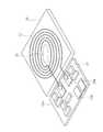
図1は、本発明の実施の形態に係る電力伝送システムの構成を示す模式図である。図1(a)は、充電台に携帯電話機を載置した状態の断面を示す模式図、図1(b)は、携帯電話機の充電台に載置する側の面の断面を示す模式図である。本発明の実施の形態に係る電力伝送システム1は、電力を供給する給電装置である充電台2、電力の供給を受ける受電装置である携帯電話機3を備える。充電台2は、平板状のコイル(第一のコイル)21、コイル21の内径部分に配置された磁石22、コイル21から供給する電力を制御する複数の電子部品23aを実装した回路基板23を備える。回路基板23は、電源であるACアダプタ4と接続されている。 FIG. 1 is a schematic diagram showing a configuration of a power transmission system according to an embodiment of the present invention. FIG. 1A is a schematic diagram showing a cross section of a state where a mobile phone is placed on a charging stand, and FIG. 1B is a schematic view showing a cross section of a surface of the mobile phone on the side where the mobile phone is placed. is there. A power transmission system 1 according to an embodiment of the present invention includes a
図2は、本発明の実施の形態に係る充電台2が備えるコイル21、磁石22、回路基板23の構成を示す模式図である。コイル21は、銅線等の導体を、同一平面で渦巻状に形成している。コイル21の外形は、略円形に形成しているが、略楕円形に形成しても、略四角形に形成しても良い。コイル21は、フェライト等の磁性体材料を粉体にして混練した硬化性樹脂で形成された樹脂構造体24に内蔵されている。ただし、コイル21は、携帯電話機3を載置する側の面にて、樹脂構造体24から露出している。なお、樹脂構造体24に代えて、コイル21の一面に磁性体シートを固着しても良い。 FIG. 2 is a schematic diagram showing the configuration of the
磁石22は、アルニコ磁石、フェライト磁石、ネオジム磁石等の永久磁石を用いて、コイル21の内径部分に配置されている。磁石22の外径は、コイル21の内径の約80%以下で、コイル21の中心を含むコイル21の内径に磁石22が配置されている。なお、磁石22の外径をコイル21の内径の約80%以下に限定しているのは、充電台2と後述する携帯電話機3との位置合わせを行う場合に、携帯電話機3のスパイラルインダクタ31をコイル21の中心に引き込むためである。 The
回路基板23は、コイル21で伝送する電力を制御する複数の電子部品23aが実装してあり、例えば、少なくとも電力制御回路、インバータ回路を構成する電子部品23aを実装してある。回路基板23は、コイル21との接続のためのコネクタ23bと、ACアダプタ4との接続のためのコネクタ23cとを設けてある。 The
図1に戻って、携帯電話機3は、スパイラルインダクタ(第二のコイル)31、スパイラルインダクタ31と離隔して配置され、二次電池32を収納している電池収納部33を備える。スパイラルインダクタ31は、軟磁性体層31a、コイル導体31bとで構成され、コイル導体31bの外径は、充電台2のコイル21の内径と略同じであるか、又は該内径より小さい。コイル導体31bの外径を、充電台2のコイル21の内径と略同じ又は該内径より小さくすることでスパイラルインダクタ31を小型化することができ、スパイラルインダクタ31を組み込んだ携帯電話機3を小型化することができる。なお、充電台2のコイル21に対してスパイラルインダクタ31のコイル導体31bを小さくすると、充電台2のコイル21と携帯電話機3のスパイラルインダクタ31とを電磁結合させて電力を伝送する場合の結合係数が低下して、電力を伝送する能力(伝送効率)が低下する。しかし、本発明の実施の形態に係る電力伝送システム1では、充電台2のコイル21の内径部分に磁石22を配置することにより、エネルギーの保持と損失との関係を示す指標であるQ値を高くすることができるため、電力を伝送する能力を維持することができる。 Returning to FIG. 1, the
また、スパイラルインダクタ31を小型化することで、スパイラルインダクタ31を、二次電池32を収納している電池収納部33と離隔して配置することが可能となる。つまり、スパイラルインダクタ31を電池収納部33に接触することなく配置することで、充電台2から電力の供給を受けてスパイラルインダクタ31が発熱しても電池収納部33に熱が伝わりにくく、二次電池32の劣化を抑えることができる。 Further, by reducing the size of the
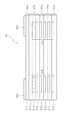
さらに、スパイラルインダクタ31について詳しく説明する。図3は、本発明の実施の形態に係るスパイラルインダクタ31の構成を示す断面図である。図4は、本発明の実施の形態に係るスパイラルインダクタ31の構成を分解して示す平面図である。図4(a)は第一層311を、図4(b)は第二層312を、図4(c)は第三層313を、図4(d)は第四層314を、図4(e)は第五層315を、図4(f)は第六層316を、図4(g)は第七層317を、図4(h)は第八層318を、それぞれ示している。図3に示すように、スパイラルインダクタ31は、八つの層311〜318、第一層311の一方の面に形成されたランド電極320で構成されている。第一層311は、非磁性フェライトからなる非磁性体層31cである。第二層312は、透磁率の高い軟磁性材料(例えば、Ni−Zn−Cuフェライト等のフェライト系材料)からなる軟磁性体層31aである。透磁率の高い軟磁性材料からなる軟磁性体層31aの第三層313、第四層314、第六層316及び第七層317に、導電性材料(例えば、Cu等)からなるコイル導体31bが形成されている。非磁性フェライトからなる非磁性体層31cの第五層315及び第八層318に、導電性材料からなるコイル導体31bが形成されている。 Further, the
軟磁性体層31a及び非磁性体層31cに形成されているコイル導体31bは、半径r1の円形の一部を欠いた形状を有し、それぞれの層に形成されたコイル導体31bは、互いに電気的に接続されて一つのコイルを構成している。第三層313及び第八層318に形成されているコイル導体31bには引き出し配線31dが設けられている。第一層311乃至第八層318は、それぞれの層に形成されたコイル導体31bは、中心を通る法線を共有するように積層され、スパイラルインダクタ31を構成している。第三層313のコイル導体31bに設けられた引き出し配線31dが一つのコイルの一端であり一方のランド電極320に接続されている。第八層318に形成されているコイル導体31bに設けられた引き出し配線31dが一つのコイルの他端であり他方のランド電極320に接続されている。なお、図3及び図4で示したスパイラルインダクタ31の構成は例示であり、軟磁性体層31aとコイル導体31bとで構成されたスパイラルインダクタ31であれば、特に限定されない。 The
また、図3に示すスパイラルインダクタ31は、コイル導体31bが形成されていない軟磁性体層31aの第二層312を備えることで、ランド電極320が形成されている面側から漏れる磁束を、ランド電極320が形成されていない面側から漏れる磁束に比べて小さくすることができる。ランド電極320が形成されていない面側が、充電台2に対向している面側となるので、スパイラルインダクタ31は、充電台2に対向している面側の漏れ磁束が、対向している該面側とは反対の面側の漏れ磁束に比べて大きくしてある。そのため、本発明の実施の形態に係る電力伝送システム1は、スパイラルインダクタ31の、充電台2に対向している面側とは反対の面側からの磁束の漏れを抑えて、充電台2のコイル21との電磁結合に利用される磁束を大きくすることができ、電力を伝送する能力を維持することができる。 Further, the
図1に戻って、スパイラルインダクタ31は、充電台2に対向している面側とは反対の面側に、回路基板34を実装するようにしてある。回路基板34は、スパイラルインダクタ31で伝送する電力を制御する複数の電子部品を実装しており、少なくとも整流回路、レギュレータ回路、充電制御回路を構成する電子部品が実装されている。図5は、本発明の実施の形態に係る電力伝送システム1の回路構成の一部を示す回路図である。図5に示す電力伝送システム1では、充電台2のコイル21と携帯電話機3のスパイラルインダクタ31とを電磁結合させて電力を伝送する場合に、スパイラルインダクタ31に接続される回路構成が図示されている。具体的には、整流回路を構成するダイオードD及びコンデンサCが回路基板34に実装され、該回路基板34を、スパイラルインダクタ31の、充電台2に対向している面側とは反対の面側に実装してある。そのため、スパイラルインダクタ31と回路基板34とで構成されるコイルモジュールを小型化して、携帯電話機3を小型化することができる。 Returning to FIG. 1, the
以上のように、本発明の実施の形態に係る電力伝送システム1では、充電台2が、平板状のコイル(第一のコイル)21と、コイル21の内径部分に配置された磁石22とを備え、携帯電話機3が、コイル21の内径と略同じ又は該内径より小さい外径のスパイラルインダクタ(第二のコイル)31を備える。スパイラルインダクタ31がコイル21より小さいため、充電台2のコイル21と携帯電話機3のスパイラルインダクタ31との結合係数は低下するが、コイル21の内径部分に配置された磁石22により、エネルギーの保持と損失との関係を示す指標であるQ値を高くすることができるため、電力を伝送する能力を維持することができる。具体的に、コイル21の外径を4cm、スパイラルインダクタ31のコイル導体31bの外径を1cmとした場合、充電台2から2.5Wの電力を供給すると、携帯電話機3で1Wの電力の供給を受けることができ、本発明の実施の形態に係る電力伝送システム1の電力を伝送する能力(伝送効率)は40%となる。 As described above, in the power transmission system 1 according to the embodiment of the present invention, the charging
また、本発明の実施の形態に係る電力伝送システム1では、充電台2のコイル21の内径部分に配置された磁石22と、携帯電話機3のスパイラルインダクタ31の軟磁性体層31aとの間の引き合う力を利用して、充電台2のコイル21と携帯電話機3のスパイラルインダクタ31との位置合わせを容易に行うことができる。さらに、本発明の実施の形態に係る電力伝送システム1では、携帯電話機3のコイルをスパイラルインダクタ31とすることで、携帯電話機3側のコイルを小型化することができる。 Moreover, in the power transmission system 1 according to the embodiment of the present invention, the gap between the
また、本発明の実施の形態に係る充電台2は、軟磁性体層31aとコイル導体31bとで構成されたスパイラルインダクタ31を備える携帯電話機3に対して、電力を供給する充電台である。そして、充電台2は、平板状のコイル21と、該コイル21の内径部分に配置された磁石22とを備える。コイル21の内径は、携帯電話機3のコイル導体31bの外径と略同じ又は該外径より大きいので、充電台2のコイル21と携帯電話機3のコイル導体31bとの結合係数は低下するが、コイル21の内径部分に配置された磁石22により、Q値を高くすることができるため、電力を伝送する能力を維持することができる。 The charging
さらに、本発明の実施の形態に係る携帯電話機3は、平板状のコイル21と、該コイル21の内径部分に配置された磁石22とを備える充電台2から電力の供給を受ける携帯電話機3である。そして、携帯電話機3は、軟磁性体層31aとコイル導体31bとで構成されたスパイラルインダクタ31と、スパイラルインダクタ31と離隔して配置され、二次電池32を収納している電池収納部33とを備えるので、充電台2から電力の供給を受けてスパイラルインダクタ31が発熱しても電池収納部33に熱が伝わりにくく、二次電池32の劣化を抑えることができる。 Furthermore, the
1 電力伝送システム
2 充電台
3 携帯電話機
4 ACアダプタ
21 コイル
22 磁石
23、34 回路基板
23a 電子部品
23b、23c コネクタ
24 樹脂構造体
31 スパイラルインダクタ
31a 軟磁性体層
31b コイル導体
31c 非磁性体層
31d 引き出し配線
32 二次電池
33 電池収納部
320 ランド電極DESCRIPTION OF SYMBOLS 1 Electric
Claims (5)
Translated fromJapanese前記給電装置は、
平板状の第一のコイルと、
該第一のコイルの内径部分に配置された磁石と
を備え、
前記受電装置は、
前記第一のコイルの内径と略同じ又は該内径より小さい外径の第二のコイルを備え、
該第二のコイルは、軟磁性体層とコイル導体とで構成されたスパイラルインダクタであることを特徴とする電力伝送システム。In a power transmission system including a power supply device that supplies power and a power receiving device that receives power supply,
The power supply device
A flat first coil;
A magnet disposed on the inner diameter portion of the first coil,
The power receiving device is:
A second coil having an outer diameter substantially the same as or smaller than the inner diameter of the first coil;
The power transmission system, wherein the second coil is a spiral inductor composed of a soft magnetic layer and a coil conductor.
平板状のコイルと、
該コイルの内径部分に配置された磁石と
を備え、
前記コイルの内径は、前記受電装置の前記コイル導体の外径と略同じ又は該外径より大きいことを特徴とする給電装置。A power supply device that supplies power to a power receiving device including a spiral inductor composed of a soft magnetic layer and a coil conductor,
A flat coil;
A magnet disposed on the inner diameter portion of the coil,
An inner diameter of the coil is substantially equal to or larger than an outer diameter of the coil conductor of the power receiving apparatus.
該コイルの内径部分に配置された磁石と
を備える給電装置から電力の供給を受ける携帯機器であって、
軟磁性体層とコイル導体とで構成されたスパイラルインダクタと、
該スパイラルインダクタと離隔して配置され、二次電池を収納している電池収納部と
を備え、
前記コイル導体の外径は、前記給電装置の前記コイルの内径と略同じ又は該内径より小さいことを特徴とする携帯機器。A flat coil;
A portable device that is supplied with electric power from a power supply device including a magnet disposed on an inner diameter portion of the coil,
A spiral inductor composed of a soft magnetic layer and a coil conductor;
A battery storage section that is spaced apart from the spiral inductor and stores a secondary battery;
The portable device characterized in that an outer diameter of the coil conductor is substantially the same as or smaller than an inner diameter of the coil of the power feeding device.
Priority Applications (1)
| Application Number | Priority Date | Filing Date | Title |
|---|---|---|---|
| JP2010145731AJP2012010533A (en) | 2010-06-28 | 2010-06-28 | Power transmission system, and power supply device and portable apparatus therefor |
Applications Claiming Priority (1)
| Application Number | Priority Date | Filing Date | Title |
|---|---|---|---|
| JP2010145731AJP2012010533A (en) | 2010-06-28 | 2010-06-28 | Power transmission system, and power supply device and portable apparatus therefor |
Publications (1)
| Publication Number | Publication Date |
|---|---|
| JP2012010533Atrue JP2012010533A (en) | 2012-01-12 |
Family
ID=45540419
Family Applications (1)
| Application Number | Title | Priority Date | Filing Date |
|---|---|---|---|
| JP2010145731APendingJP2012010533A (en) | 2010-06-28 | 2010-06-28 | Power transmission system, and power supply device and portable apparatus therefor |
Country Status (1)
| Country | Link |
|---|---|
| JP (1) | JP2012010533A (en) |
Cited By (11)
| Publication number | Priority date | Publication date | Assignee | Title |
|---|---|---|---|---|
| WO2014002374A1 (en)* | 2012-06-28 | 2014-01-03 | パナソニック株式会社 | Mobile terminal |
| WO2014050352A1 (en)* | 2012-09-27 | 2014-04-03 | Tanaka Tetsuo | Stand for portable electronic device |
| EP2642632A3 (en)* | 2012-03-23 | 2014-07-30 | LG Innotek Co., Ltd. | Wireless power receiver and method of manufacturing the same |
| US9553476B2 (en) | 2012-03-23 | 2017-01-24 | Lg Innotek Co., Ltd. | Antenna assembly and method for manufacturing same |
| US9607757B2 (en) | 2011-11-02 | 2017-03-28 | Panasonic Corporation | Non-contact wireless communication coil, transmission coil, and portable wireless terminal |
| US9735606B2 (en) | 2012-06-28 | 2017-08-15 | Panasonic Intellectual Property Management Co., Ltd. | Mobile terminal including charging coil and wireless communication coil, wireless charging module including charging coil and wireless communication coil |
| US9935481B2 (en) | 2012-02-17 | 2018-04-03 | Panasonic Intellectual Property Management Co., Ltd. | Mobile terminal including wireless charging module and battery pack |
| US9954396B2 (en) | 2011-06-14 | 2018-04-24 | Panasonic Corporation | Electronic device including non-contact charging module |
| JP2018088471A (en)* | 2016-11-28 | 2018-06-07 | 京セラ株式会社 | Printed wiring board |
| US10204734B2 (en) | 2011-11-02 | 2019-02-12 | Panasonic Corporation | Electronic device including non-contact charging module and near field communication antenna |
| US10218222B2 (en) | 2011-01-26 | 2019-02-26 | Panasonic Intellectual Property Management Co., Ltd. | Non-contact charging module having a wireless charging coil and a magnetic sheet |
Citations (4)
| Publication number | Priority date | Publication date | Assignee | Title |
|---|---|---|---|---|
| JPH113829A (en)* | 1997-06-11 | 1999-01-06 | Tokin Corp | Laminated coil part and battery charger incorporating the same |
| WO2009025279A1 (en)* | 2007-08-21 | 2009-02-26 | Kabushiki Kaisha Toshiba | Noncontact power receiving apparatus, electronic device using noncontact power receiving apparatus and charging system |
| JP2009159660A (en)* | 2007-12-25 | 2009-07-16 | Casio Comput Co Ltd | Non-contact power transmission device |
| JP2009188131A (en)* | 2008-02-05 | 2009-08-20 | Nec Tokin Corp | Non-contact power transmission device |
- 2010
- 2010-06-28JPJP2010145731Apatent/JP2012010533A/enactivePending
Patent Citations (4)
| Publication number | Priority date | Publication date | Assignee | Title |
|---|---|---|---|---|
| JPH113829A (en)* | 1997-06-11 | 1999-01-06 | Tokin Corp | Laminated coil part and battery charger incorporating the same |
| WO2009025279A1 (en)* | 2007-08-21 | 2009-02-26 | Kabushiki Kaisha Toshiba | Noncontact power receiving apparatus, electronic device using noncontact power receiving apparatus and charging system |
| JP2009159660A (en)* | 2007-12-25 | 2009-07-16 | Casio Comput Co Ltd | Non-contact power transmission device |
| JP2009188131A (en)* | 2008-02-05 | 2009-08-20 | Nec Tokin Corp | Non-contact power transmission device |
Cited By (36)
| Publication number | Priority date | Publication date | Assignee | Title |
|---|---|---|---|---|
| US10218222B2 (en) | 2011-01-26 | 2019-02-26 | Panasonic Intellectual Property Management Co., Ltd. | Non-contact charging module having a wireless charging coil and a magnetic sheet |
| US9954396B2 (en) | 2011-06-14 | 2018-04-24 | Panasonic Corporation | Electronic device including non-contact charging module |
| US10003219B1 (en) | 2011-06-14 | 2018-06-19 | Panasonic Corporation | Electronic device including non-contact charging module |
| US10044225B2 (en) | 2011-06-14 | 2018-08-07 | Panasonic Corporation | Electronic device including non-contact charging module |
| US10468913B2 (en) | 2011-06-14 | 2019-11-05 | Sovereign Peak Ventures, Llc | Electronic device including non-contact charging module |
| US10204734B2 (en) | 2011-11-02 | 2019-02-12 | Panasonic Corporation | Electronic device including non-contact charging module and near field communication antenna |
| US9634515B2 (en) | 2011-11-02 | 2017-04-25 | Panasonic Corporation | Non-contact wireless communication coil, transmission coil, and portable wireless terminal |
| US9607757B2 (en) | 2011-11-02 | 2017-03-28 | Panasonic Corporation | Non-contact wireless communication coil, transmission coil, and portable wireless terminal |
| US9941048B2 (en) | 2011-11-02 | 2018-04-10 | Panasonic Corporation | Non-contact wireless communication coil, transmission coil, and portable wireless terminal |
| US9997952B2 (en) | 2012-02-17 | 2018-06-12 | Panasonic Intellectual Property Management Co., Ltd. | Wireless charging module and mobile terminal including the same |
| US10574082B2 (en) | 2012-02-17 | 2020-02-25 | Sovereign Peak Ventures, Llc | Electronic device including non-contact charging module and battery |
| US10020673B2 (en) | 2012-02-17 | 2018-07-10 | Panasonic Intellectual Property Management Co., Ltd. | Electronic device including non-contact charging module and battery |
| US11070075B2 (en) | 2012-02-17 | 2021-07-20 | Sovereign Peak Ventures, Llc | Electronic device including non-contact charging module and battery |
| US9935481B2 (en) | 2012-02-17 | 2018-04-03 | Panasonic Intellectual Property Management Co., Ltd. | Mobile terminal including wireless charging module and battery pack |
| US12040562B2 (en) | 2012-02-17 | 2024-07-16 | Sovereign Peak Ventures, Llc | Electronic device including non-contact charging module and battery |
| US9991735B1 (en) | 2012-02-17 | 2018-06-05 | Panasonic Intellectual Property Management Co., Ltd. | Electronic device including non-contact charging module and battery |
| US9806565B2 (en) | 2012-03-23 | 2017-10-31 | Lg Innotek Co., Ltd. | Wireless power receiver and method of manufacturing the same |
| US10270291B2 (en) | 2012-03-23 | 2019-04-23 | Lg Innotek Co., Ltd. | Wireless power receiver and method of manufacturing the same |
| US10804740B2 (en) | 2012-03-23 | 2020-10-13 | Lg Innotek Co., Ltd. | Wireless power receiver and method of manufacturing the same |
| TWI613686B (en)* | 2012-03-23 | 2018-02-01 | Lg伊諾特股份有限公司 | Method of manufacturing a wireless power receiver |
| US10673141B2 (en) | 2012-03-23 | 2020-06-02 | Lg Innotek Co., Ltd. | Antenna assembly and method for manufacturing same |
| EP2642632A3 (en)* | 2012-03-23 | 2014-07-30 | LG Innotek Co., Ltd. | Wireless power receiver and method of manufacturing the same |
| US9553476B2 (en) | 2012-03-23 | 2017-01-24 | Lg Innotek Co., Ltd. | Antenna assembly and method for manufacturing same |
| US10277071B2 (en) | 2012-03-23 | 2019-04-30 | Lg Innotek Co., Ltd. | Wireless power receiver and method of manufacturing the same |
| US10256540B2 (en) | 2012-03-23 | 2019-04-09 | Lg Innotek Co., Ltd. | Antenna assembly and method for manufacturing same |
| US9735606B2 (en) | 2012-06-28 | 2017-08-15 | Panasonic Intellectual Property Management Co., Ltd. | Mobile terminal including charging coil and wireless communication coil, wireless charging module including charging coil and wireless communication coil |
| US10230272B2 (en) | 2012-06-28 | 2019-03-12 | Panasonic Intellectual Property Management Co., Ltd. | Mobile terminal including wireless charging coil and magnetic sheet having inwardly receding portion |
| US10291069B2 (en) | 2012-06-28 | 2019-05-14 | Panasonic Intellectual Property Management Co., Ltd. | Mobile terminal and chargeable communication module |
| US9667086B2 (en) | 2012-06-28 | 2017-05-30 | Panasonic Intellectual Property Management Co., Ltd. | Mobile terminal |
| US10574090B2 (en) | 2012-06-28 | 2020-02-25 | Sovereign Peak Ventures, Llc | Mobile terminal including wireless charging coil and magnetic sheet having inwardly receding portion |
| WO2014002374A1 (en)* | 2012-06-28 | 2014-01-03 | パナソニック株式会社 | Mobile terminal |
| JP2018029475A (en)* | 2012-06-28 | 2018-02-22 | パナソニックIpマネジメント株式会社 | Mobile device |
| US11616395B2 (en) | 2012-06-28 | 2023-03-28 | Sovereign Peak Ventures, Llc | Mobile terminal and chargeable communication module |
| JP2014011853A (en)* | 2012-06-28 | 2014-01-20 | Panasonic Corp | Portable terminal |
| WO2014050352A1 (en)* | 2012-09-27 | 2014-04-03 | Tanaka Tetsuo | Stand for portable electronic device |
| JP2018088471A (en)* | 2016-11-28 | 2018-06-07 | 京セラ株式会社 | Printed wiring board |
Similar Documents
| Publication | Publication Date | Title |
|---|---|---|
| JP2012010533A (en) | Power transmission system, and power supply device and portable apparatus therefor | |
| US8248025B2 (en) | Charging system capable of charging electronic device by electromagnetic induction | |
| CN111527666B (en) | wireless power transmission device | |
| CN203366972U (en) | Contactless charging module and receiving-side and transmission-side contactless charger using same | |
| KR102017621B1 (en) | Coil substrate for cordless charging and electric device using the same | |
| KR101198880B1 (en) | Contact-less Charging Module and Reception-side and Transmission-side Contact-less Charging Devices Using the Same | |
| US8237401B2 (en) | Recharging system and electronic device | |
| CN103782357B (en) | Power receiver side non-contact charge module and non-contact charge equipment | |
| CN208674377U (en) | Antenna devices and electronic equipment | |
| CN104025423B (en) | The forming method of magnetic field space | |
| WO2013172349A1 (en) | Antenna sheet for contactless charging device and charging device using said sheet | |
| JP4835794B1 (en) | Receiving side non-contact charging module and receiving side non-contact charging device | |
| US9270797B2 (en) | Reducing inductive heating | |
| JP5845406B2 (en) | Receiving side non-contact charging module and receiving side non-contact charging device | |
| JP2010284059A (en) | Noncontact power transmission apparatus | |
| US8771852B2 (en) | Battery pack with contactless power transfer | |
| US8855354B2 (en) | Electroacoustic transducer with wireless charging coil | |
| KR20140089192A (en) | Soft magnetic sheet, soft magnetic plate and soft magnetic pellet for antenna of wireless power receiving apparatus | |
| JP7487237B2 (en) | Portable battery pack for wirelessly charging a wearable device through clothing | |
| JP2012156280A (en) | Reception side non-contact charging module and reception side non-contact charging apparatus | |
| WO2019111848A1 (en) | Coil module | |
| JP4900525B1 (en) | Non-contact charging module, transmitting-side non-contact charging device and receiving-side non-contact charging device provided with the same | |
| KR101532052B1 (en) | Antenna patch comprising common terminals for wireless charging and nfc communication | |
| JP2012191739A (en) | Transmission coil device, and power receiving device and power feeding device using the same | |
| US10141772B2 (en) | Communication device |
Legal Events
| Date | Code | Title | Description |
|---|---|---|---|
| A621 | Written request for application examination | Free format text:JAPANESE INTERMEDIATE CODE: A621 Effective date:20130313 | |
| A977 | Report on retrieval | Free format text:JAPANESE INTERMEDIATE CODE: A971007 Effective date:20140224 | |
| A131 | Notification of reasons for refusal | Free format text:JAPANESE INTERMEDIATE CODE: A131 Effective date:20140304 | |
| A521 | Request for written amendment filed | Free format text:JAPANESE INTERMEDIATE CODE: A523 Effective date:20140414 | |
| A02 | Decision of refusal | Free format text:JAPANESE INTERMEDIATE CODE: A02 Effective date:20141111 |