JP2012004473A - Semiconductor device and method for manufacturing semiconductor device - Google Patents
Semiconductor device and method for manufacturing semiconductor deviceDownload PDFInfo
- Publication number
- JP2012004473A JP2012004473AJP2010140330AJP2010140330AJP2012004473AJP 2012004473 AJP2012004473 AJP 2012004473AJP 2010140330 AJP2010140330 AJP 2010140330AJP 2010140330 AJP2010140330 AJP 2010140330AJP 2012004473 AJP2012004473 AJP 2012004473A
- Authority
- JP
- Japan
- Prior art keywords
- insulating film
- semiconductor
- semiconductor device
- gate
- columnar
- Prior art date
- Legal status (The legal status is an assumption and is not a legal conclusion. Google has not performed a legal analysis and makes no representation as to the accuracy of the status listed.)
- Pending
Links
Images


Landscapes
- Electrodes Of Semiconductors (AREA)
- Metal-Oxide And Bipolar Metal-Oxide Semiconductor Integrated Circuits (AREA)
- Semiconductor Memories (AREA)
- Non-Volatile Memory (AREA)
- Thin Film Transistor (AREA)
- Insulated Gate Type Field-Effect Transistor (AREA)
Abstract
Translated fromJapaneseDescription
Translated fromJapanese本発明は、縦型トランジスタを有する半導体装置及び半導体装置の製造方法に関する。 The present invention relates to a semiconductor device having a vertical transistor and a method for manufacturing the semiconductor device.
リソグラフィの短波長化による集積度向上に限界が見え、平面において集積度をあげるときの難易度が飛躍的に増している。このような状況の中で、従来のプレーナー型MIS(Metal Insulator Semiconductor)FET(Field Effect Transistor)を、基板に対して略垂直に電流が流れる、いわゆる縦型MISFETに置き換えようとする試みがある。 There is a limit to the improvement of the integration degree due to the shortening of the wavelength of lithography, and the difficulty in increasing the integration degree on a plane has increased dramatically. Under such circumstances, there is an attempt to replace a conventional planar type MIS (Metal Insulator Semiconductor) FET (Field Effect Transistor) with a so-called vertical MISFET in which a current flows substantially perpendicular to the substrate.
縦型MISFETは、プレーナー型のMISFETでは得られない多くの利点を有する。例えば、微細なゲート長のFETを高価なリソグラフィ装置を用いることなく作製できることがある。また、ダブルゲート構造やゲート・オール・アラウンド構造を用いることで、ゲートの制御性を高め、短チャネル特性を改善できる。また、立体化して(積層して)高集積化が可能である。また、製造方法によってはゲート長を膜厚で規定でき、ゲート長ばらつきを小さくできる。 The vertical MISFET has many advantages that cannot be obtained with a planar MISFET. For example, a fine gate length FET may be manufactured without using an expensive lithographic apparatus. Further, by using a double gate structure or a gate all-around structure, the controllability of the gate can be improved and the short channel characteristics can be improved. Further, it can be three-dimensional (stacked) and highly integrated. Further, depending on the manufacturing method, the gate length can be defined by the film thickness, and the gate length variation can be reduced.
また、平面の占有面積に比較して、ゲート長を長くとれる。これは、集積度を可能な限り向上させながらも、ゲート長を長くしてリーク電流をさげたいDRAM(Dynamic Ramdam Access Memory)のセルトランジスタや、同様に、集積度を可能な限り向上させながらも、ゲート長を長くしてばらつきを低減したいSRAM(Static Randam Access Memory)のトランジスタに適する。 In addition, the gate length can be made longer than the plane occupation area. This is because, while improving the degree of integration as much as possible, the cell transistor of DRAM (Dynamic Random Access Memory) that wants to increase the gate length and reduce the leakage current, and similarly, while improving the degree of integration as much as possible. It is suitable for an SRAM (Static Random Access Memory) transistor whose gate length is increased to reduce variation.
しかし、縦型トランジスタは、SD(Source Drain)の寄生抵抗が大きい、という問題がある。一般に、SDの寄生抵抗を低減するには、プレーナー型MISFETのように、SDにシリサイドを形成することが行われる。 However, the vertical transistor has a problem that the parasitic resistance of SD (Source Drain) is large. In general, in order to reduce the parasitic resistance of the SD, a silicide is formed on the SD like a planar type MISFET.
例えば、特許文献1の図30から図32に製造工程の途中段階が開示されている半導体装置では、縦型MISFETの下部SD電極にシリサイドが形成されている。また下部SD電極に形成されるシリサイドの、チャネル領域からの相対的な位置は、シリサイド上に形成される絶縁膜の膜厚によって、正確に制御されている。 For example, in the semiconductor device disclosed in the middle of the manufacturing process in FIGS. 30 to 32 of
また、特許文献2の図6に開示されている半導体装置では、柱状半導体の下部SD電極の上にシリサイド層が形成されている。 In the semiconductor device disclosed in FIG. 6 of
特許文献3の図1に開示されている半導体装置では、縦型MISFETの上部SD電極、下部SD電極の双方にシリサイドが形成されている。また、上部SD電極のシリサイドと、下部SD電極のシリサイドは同時に形成される。 In the semiconductor device disclosed in FIG. 1 of
縦型トランジスタのSDの寄生抵抗を十分に下げるためには、上部SD電極と下部SD電極のシリサイドの位置を、プレーナー型MISFETと同じくらい、チャネル領域に近づけることが重要である。このためには、上部SD電極と下部SD電極それぞれにおいて、シリサイドの位置を精度よく制御できるようにする必要がある。このため、シリサイドの位置を精度よく制御できるようにすることが望まれている。 In order to sufficiently reduce the parasitic resistance of the SD of the vertical transistor, it is important that the silicide positions of the upper SD electrode and the lower SD electrode are as close to the channel region as the planar MISFET. For this purpose, it is necessary to accurately control the position of the silicide in each of the upper SD electrode and the lower SD electrode. For this reason, it is desired to be able to control the position of the silicide with high accuracy.
本発明によれば、柱状半導体と、
前記柱状半導体の側面の一部に接するゲート絶縁膜と、
前記ゲート絶縁膜のうち前記柱状半導体とは逆側の面に接するゲートと、
前記ゲートの上及び下それぞれに形成され、前記ゲート及び前記ゲート絶縁膜に接している第1絶縁膜と、
前記柱状半導体の前記側面のうち、前記ゲートに面する領域より上側の領域及び下側の領域それぞれに形成されており、前記柱状半導体の前記側面のうち前記第1絶縁膜に対向する領域に接しているシリサイドと、
を備える半導体装置が提供される。According to the present invention, a columnar semiconductor;
A gate insulating film in contact with a part of the side surface of the columnar semiconductor;
A gate in contact with a surface of the gate insulating film opposite to the columnar semiconductor;
A first insulating film formed on and under the gate, and in contact with the gate and the gate insulating film;
Of the side surface of the columnar semiconductor, formed on each of a region above and below a region facing the gate, and is in contact with a region of the side surface of the columnar semiconductor facing the first insulating film. With silicide,
A semiconductor device is provided.
本発明によれば、第1絶縁膜の厚さによって、ゲートからシリサイドまでの距離を制御することができる。絶縁膜の厚さは一般的に高精度に制御できる。従って、ゲートからシリサイドまでの位置を精度よく制御できる。 According to the present invention, the distance from the gate to the silicide can be controlled by the thickness of the first insulating film. In general, the thickness of the insulating film can be controlled with high accuracy. Therefore, the position from the gate to the silicide can be accurately controlled.
本発明によれば、柱状半導体と、前記柱状半導体の側面のうち上端及び下端から離れた領域に面していて第1の第1絶縁膜、ゲート層、及び第2の第1絶縁膜からなる第1の積層構造とを形成する第1工程と、
前記柱状半導体の側面のうち前記第1の第1絶縁膜、前記ゲート層、及び前記第2の第1絶縁膜に面していない領域に金属層を形成する第2工程と、
熱処理を行うことにより、前記金属層と前記柱状半導体とを反応させてシリサイドを形成する第3工程と、
を備える半導体装置の製造方法が提供される。According to the present invention, the columnar semiconductor and the side surface of the columnar semiconductor facing the region away from the upper end and the lower end are formed of the first first insulating film, the gate layer, and the second first insulating film. A first step of forming a first laminated structure;
Forming a metal layer in a region of the side surface of the columnar semiconductor that does not face the first first insulating film, the gate layer, and the second first insulating film;
A third step of forming silicide by reacting the metal layer and the columnar semiconductor by performing heat treatment;
A method for manufacturing a semiconductor device is provided.
本発明によれば、縦型のトランジスタにおいてゲートからシリサイドまでの位置を精度よく制御できる。 According to the present invention, the position from the gate to the silicide in the vertical transistor can be accurately controlled.
以下、本発明の実施の形態について、図面を用いて説明する。尚、すべての図面において、同様な構成要素には同様の符号を付し、適宜説明を省略する。 Hereinafter, embodiments of the present invention will be described with reference to the drawings. In all the drawings, the same reference numerals are given to the same components, and the description will be omitted as appropriate.
(第1の実施形態)
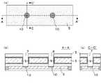
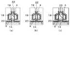
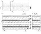
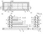
図1(a)は、本発明の第1の実施形態である半導体装置の上面図である。また、図1(b)は、図1(a)のA−A´線に沿った断面図、図1(c)は、図1(a)のC−C´線に沿った断面図である。本実施形態の半導体装置は、n型MISFETであっても、p型MISFETであってもかまわない。ここでは、n型MISFETを一例として説明する。また本図に示す半導体装置は、MISFETを同一層に複数有する。(First embodiment)
FIG. 1A is a top view of the semiconductor device according to the first embodiment of the present invention. 1B is a cross-sectional view taken along the line AA ′ in FIG. 1A, and FIG. 1C is a cross-sectional view taken along the line CC ′ in FIG. is there. The semiconductor device of this embodiment may be an n-type MISFET or a p-type MISFET. Here, an n-type MISFET will be described as an example. Further, the semiconductor device shown in this drawing has a plurality of MISFETs in the same layer.
本実施形態の半導体装置では、半導体基板1または半導体層にn型拡散層(不純物領域)3が形成されている。n型拡散層(不純物領域)3は、その周囲を素子分離絶縁膜2に囲まれている。また、n型拡散層(不純物領域)3の上には、柱状半導体14が形成されている。1つの柱状半導体14は、1つの縦型MISFETを構成している。詳細には、柱状半導体14の上部と下部には、それぞれSD電極となるn型拡散層19が形成されている。また柱状半導体14の中央部はチャネル領域となっている。 In the semiconductor device of this embodiment, an n-type diffusion layer (impurity region) 3 is formed in the
柱状半導体14の中央部には、その周囲を囲むように、ゲート絶縁膜9が熱酸化法により形成され、さらに、ゲート絶縁膜9の周囲を囲むように、ゲート層6が形成されている。この柱状半導体14の中央部、ゲート絶縁膜9、ゲート層6により、MIS構造が形成されている。ゲート層6の上下には、第1絶縁膜4が形成されている。第1絶縁膜4は、柱状半導体14にも接している。第1絶縁膜4は、ゲート層6の上及び下それぞれに形成されており、かつゲート層6及びゲート絶縁膜9に接している。柱状半導体14の側面には、シリサイド18及びn型拡散層(不純物領域)19が形成されている。n型拡散層19は、シリサイド18の周囲に形成されている。シリサイド18は、第1絶縁膜4によってセルフ・アラインされた位置に形成されている。上側の第1絶縁膜4によってセルフ・アラインされた位置に形成されたシリサイド18は、柱状半導体14の天面まで連続して形成されている。また、下側の第1絶縁膜4によってセルフ・アラインされた位置に形成されたシリサイド18は、半導体基板1のn型拡散層3まで連続して形成されている。なおシリサイド18は、柱状半導体14の側面のうち、第1絶縁膜4に対向している領域に接している。 In the central portion of the
また、シリサイド18は、ゲート層6の上面および側面にも形成されている。上部SD電極となるn型拡散層19への接続は、柱状半導体14の天面に形成されたシリサイド18に対してコンタクト22を接続することで、行われる。下部SD電極となるn型拡散層19への接続は、半導体基板1のn型拡散層(不純物領域)3に形成されたシリサイド18に対してコンタクト22を接続することで行われる。ゲート層6への接続は、ゲート層6に形成されたシリサイド18に対してコンタクト22を接続することで、行われる。コンタクト22は、いずれも、層間絶縁膜21、ストッパー絶縁膜20を貫く形で、各部のシリサイド18に接続する。 The
なお、図1には柱状半導体14が2つ存在している。それぞれの柱状半導体は、1つの縦型MISFETを構成し、2つの縦型MISFETのゲート同士、下部電極同士が接続された形となっている。本発明の半導体装置は、図1の左半分、右半分の縦型MISFETで必要十分であるが、後で説明するように、作製途中でゲート層6が梁構造となるため、付着現象がおきにくくなる構造が好ましい。この意味で、図1に示すように2つの縦型MISFETのゲート層6同士を接続した構造を示している。なお、後述するように、付着現象がおきないようにプロセスに配慮すれば、もしくは、ゲート層6が片持ち梁構造になっても付着しない構造であれば、電気的な接続が必要な場合を除いて、特にゲート同士を接続する必要はない。 In FIG. 1, two
以下に、各部の詳細について、説明する。 Details of each part will be described below.
半導体基板1は、単結晶半導体のバルク基板、又は表面に単結晶半導体層が形成された基板、例えばSOI(Silicon on Insulator)基板とするのが好ましい。半導体基板1は、バルクSi(100)基板のほか、(110)、(111)などの面方位をもつバルクSi基板、または、任意の材料で形成された基板の表面に(100)、(110)、(111)などの面方位をもつSiが形成された基板とすることができる。基板のドーピング型、濃度、ノッチ(オリフラ)方向については、特に限定されない。また、必ずしも表面に単結晶半導体層が形成されていなくてもよい。多結晶半導体層、非晶質半導体層であってもよい。すなわち、トランジスタが形成された上に絶縁膜を介して、多結晶半導体層ないしは非晶質半導体層を形成したような基板も、本実施形態の半導体基板1として用いることが可能である。 The
柱状半導体14は、単結晶半導体、多結晶半導体、及び非晶質半導体のいずれでも構わない。ただし、半導体基板1の表面が単結晶半導体層でない場合、柱状半導体14は、単結晶半導体にならず、多結晶半導体ないしは非晶質半導体になる。柱状半導体14の材料は、半導体基板1と同じにするのが一般的である。すなわち、半導体基板1がバルクSi(100)基板ならば、柱状半導体14の材料もSiとするのが一般的である。ただし、半導体基板1と柱状半導体14とは別の材料で形成してもかまわない。この場合は、半導体基板1の材料から、組成を一部変更したような材料とするのがよい。すなわち、半導体基板1がバルクSi(100)基板ならば、柱状半導体14の材料をSiGeやSiCとしてもよい。また柱状半導体14は、縦型MISFETのチャネル領域を構成するので、通常、しきい値電圧調整用のドーピングが行われている。 The
シリサイド18は、柱状半導体14の天面、側面、ゲート層6の上面、側面、半導体基板1のn型拡散層(不純物領域)3の各所に形成されている。このうち、柱状半導体14の側面に形成されたシリサイド18は、ゲート層6の上下それぞれに形成された第1絶縁膜4に対して、セルフ・アラインされた位置に形成されている。このため、第1絶縁膜4の膜厚を変化させることで、シリサイド18の、チャネル領域からの相対的な位置を任意に設定できる。このため、これまでの縦型MISFETと比較して、チャネル領域により近い位置に、シリサイドを形成できる。このため、SDの寄生抵抗を低減できる。シリサイド18は、Niシリサイド、Ptシリサイド、Coシリサイド、Tiシリサイド、Wシリサイド、Pdシリサイド、Erシリサイド、などであるが、これらに限定されない。また、これらの合金のシリサイドでもよい。合金のシリサイドの例として、NiPtシリサイドがあげられる。なお後で説明するように、CVD(Chemical Vapor Deposition)で柱状半導体14の側面に、シリサイド金属を成膜するので、シリサイド金属を含んだCVD原料が存在していることが前提になる。 The
第1絶縁膜4は、柱状半導体14の側面に形成されるシリサイド18の、チャネル領域からの相対的な位置を調整する役割を果たす。その厚みが、プレーナー型MISFETのSW(サイドウォール)幅に相当する。プレーナー型MISFETのSWとの違いは、以下の2点が挙げられる。第1に、プレーナー型MISFETのSWの場合、成膜とエッチバックの2工程でSW幅が決まるのに対して、本発明の半導体装置では、成膜のみで決まっているので精度がよくばらつきが少ない。第2にプレーナー型MISFETのSWの場合、ゲートをはさんだ2つのSWの幅は常に同じになるのに対して、本発明の半導体装置では、ゲート層6の上下の第1絶縁膜4の膜厚を必ずしも同じにしなくてもよい。後者の違いから、本発明の半導体装置の場合、設計の自由度が広がる。例えば、SDを形成する、あるドーパントが柱状半導体14の上部方向に拡散しやすい特性を持っていたとする。この場合、下側の第1絶縁膜4の膜厚を上側の第1絶縁膜4の膜厚より厚くすることで、SDとゲート層6の重なりが上下で同じになるように調整できる。 The first
ゲート層6は、その膜厚が縦型MISFETのゲート長となる。ゲート層6は、一般に、多結晶半導体もしくは非晶質半導体であり、その材料は、半導体基板1と同じである。すなわち、通常、多結晶Si、もしくは、非晶質Siである。しかし、これらに限定されず、例えば、多結晶SiGe、もしくは、非晶質SiGeのように、半導体基板1と異なる材料であってもよい。また、図1では、ゲート層6の上部と側面にシリサイド18が形成されているが、ゲート層6のすべての部分をシリサイド化して、メタルゲートとしてもかまわない。例えば、Niシリサイドからなるメタルゲートとしてもよい。 The thickness of the
ゲート絶縁膜9は、その膜の種類として、Si酸化膜、Si酸窒化膜、Si窒化膜、Ta2O5、Al2O3、HfO2、ZrO2、ZrON、HfON、HfAlON、HfSiON、HfAlSiONなどのHigh−k膜があげられるが、これらに限定されない。またゲート絶縁膜9は単層膜である必要はなく、任意の絶縁膜の積層膜でもよい。ゲート絶縁膜9を酸化、もしくは酸窒化で形成する場合は、図1のように、ゲート層6の端面に形成される。ゲート絶縁膜9をCVDで形成する場合は、図43を用いて後述するように、ゲート絶縁膜9が、ゲート層6の端面だけでなく、ゲート層6の上下の第1絶縁膜4の端面にも形成される形となる。なお、ゲート絶縁膜9として、Si酸化膜とSi窒化膜の積層膜(ONO膜)を用いると、本発明の縦型MISFETを記憶素子とすることができる。The
n型拡散層(不純物領域)19は、後述するように、シリサイド形成時の雪かき効果で形成される。したがって、柱状半導体14のしきい値電圧調整用のp型ドーピングが施されている領域とは、急峻な接合界面を形成する。そのため、微細なゲート長を持つFETの浅接合としても適用可能である。 As will be described later, the n-type diffusion layer (impurity region) 19 is formed by a snow removal effect during silicide formation. Therefore, a steep junction interface is formed with the region where the p-type doping for adjusting the threshold voltage of the
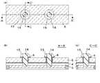
図43(a)は、図1に示した半導体装置の変形例の上面図である。また、図43(b)は、図43(a)のA−A´線に沿った断面図、図43(c)は、図43(a)のC−C´線に沿った断面図である。本図に示す半導体装置は、ゲート絶縁膜9と第1絶縁膜4の位置関係を除いて、図1に示した半導体装置と同胞の構造を有している。 FIG. 43A is a top view of a modification of the semiconductor device shown in FIG. 43B is a cross-sectional view taken along the line AA ′ in FIG. 43A, and FIG. 43C is a cross-sectional view taken along the line CC ′ in FIG. is there. The semiconductor device shown in this figure has the same structure as the semiconductor device shown in FIG. 1 except for the positional relationship between the
詳細には、図43においてゲート絶縁膜9は、気相成長法、例えばCVD法により形成されている。そしてゲート6及び第1絶縁膜4は、いずれもゲート絶縁膜9を介して柱状半導体14の側面に面している。シリサイド18は、柱状半導体14の側面のうちゲート絶縁膜9に覆われていない領域に形成されている。 Specifically, in FIG. 43, the
以下、図2から図19を用いて、本実施形態の半導体装置の製造方法の一例についてより詳細に説明する。図2から図19は、本実施形態の縦型MISFETの製造工程における各段階の状態の一例を示す模式図である。各図の(a)が上面図、各図の(b)が各図の(a)のA−A´線に沿った断面図、各図の(c)が各図の(a)のC−C´線に沿った断面図である。本実施形態の製造方法は、n型MISFETにも、p型MISFETにも適用可能である。ここでは、n型MISFETの製造方法を一例として説明する。 Hereinafter, an example of the method for manufacturing the semiconductor device according to the present embodiment will be described in more detail with reference to FIGS. 2 to 19 are schematic views showing an example of the state of each stage in the manufacturing process of the vertical MISFET of this embodiment. (A) of each figure is a top view, (b) of each figure is a cross-sectional view taken along the line AA 'of (a) of each figure, (c) of each figure is C of (a) of each figure. It is sectional drawing along a -C 'line. The manufacturing method of the present embodiment can be applied to an n-type MISFET and a p-type MISFET. Here, an n-type MISFET manufacturing method will be described as an example.
まず、図2に示すように、半導体基板1に素子分離絶縁膜2を形成する。以下では、半導体基板1を、最も一般的なp型単結晶Si(100)基板として説明する。素子分離絶縁膜2の形成は、例えばSTI(Shallow Trench Isolation)法、または、LOCOS(Local Oxidation of Silicon)法を用いる。 First, as shown in FIG. 2, an element
次いで図3に示すように、n型拡散層(不純物領域)3を形成する。具体的には、n型のドーパント(P、Asなど)をイオン注入し、イオン注入後、熱処理により、これらのドーパントを活性化する。例えば、1価のAsイオンを注入し、窒素雰囲気もしくは、窒素雰囲気に微量の酸素が混入された雰囲気で、1050℃のスパイクアニールを行う。スパイクアニールは、例えば、目的の温度まで、装置の最大もしくは最大に近い昇温レートで昇温して、目的の温度での維持時間を0秒とし、装置の最大もしくは最大に近い降温レートで降温する熱処理である。 Next, as shown in FIG. 3, an n-type diffusion layer (impurity region) 3 is formed. Specifically, n-type dopants (P, As, etc.) are ion-implanted, and after the ion implantation, these dopants are activated by heat treatment. For example, monovalent As ions are implanted, and spike annealing at 1050 ° C. is performed in a nitrogen atmosphere or an atmosphere in which a small amount of oxygen is mixed in the nitrogen atmosphere. Spike annealing, for example, raises the temperature up to the target temperature at the maximum or near maximum temperature rise rate, sets the maintenance time at the target temperature to 0 seconds, and drops the temperature at the maximum or maximum temperature drop rate of the device. Heat treatment.
次いで図4に示すように、n型拡散層(不純物領域)3の上に、ゲート層6を第1絶縁膜4で挟み、これを第2絶縁膜5で挟んだ積層体を形成する。具体的には、下側の第2絶縁膜5、下側の第1絶縁膜4、ゲート層6、上側の第1絶縁膜4、及び上側の第2絶縁膜5をこの順に積層する。上記したように、2つの第1絶縁膜4それぞれの膜厚を調整することにより、シリサイドとチャネル領域の相対的な位置を調整できる。2つの第2絶縁膜5は、その膜厚で、縦型MISFETのSDに形成されるシリサイドの長さを決定する。後工程において、ゲート層6を第1絶縁膜4で保護した状態で、第2絶縁膜5を除去する。したがって、第2絶縁膜5は、第1絶縁膜4に対して、選択エッチングが可能な材料でなければならない。なお、第1絶縁膜4の厚みは、ゲート層6の上下で必ずしも同じである必要はない。また同様に、第2絶縁膜5の厚みも、上下で必ずしも同じである必要はない。 Next, as shown in FIG. 4, a stacked body is formed on the n-type diffusion layer (impurity region) 3 with the
ゲート層6の例としては、多結晶Siもしくは非晶質Siがあげられる。第1絶縁膜4と第2絶縁膜5の組み合わせの例としては、第1絶縁膜4をSi酸化膜、第2絶縁膜5をSi窒化膜とする例があげられる。また、この逆でもかまわない。ただし、逆の場合は、後工程で、第2絶縁膜5として、Si酸化膜を除去することになり、素子分離絶縁膜2の膜減りを考慮して、素子分離絶縁膜2を作製する必要がある。以後、第1絶縁膜4をSi酸化膜、第2絶縁膜5をSi窒化膜、ゲート層6を多結晶Siとして、説明を続ける。この場合、減圧CVDを用いて、第2絶縁膜5としてSi窒化膜、第1絶縁膜4としてSi酸化膜、ゲート層6として多結晶Si膜、第1絶縁膜4としてSi酸化膜、第2絶縁膜5としてSi窒化膜を、この順に成膜していく。 Examples of the
次いで図5に示すように、第2絶縁膜5の成膜後、レジスト塗布、露光、現像という一連のリソグラフィ工程を行って、所望の開口部分のレジストが残らないようなレジストパターン(未図示)を、上側の第2絶縁膜5の上に作製する。その後、このレジストパターンをマスクとして、第2絶縁膜5、第1絶縁膜4、ゲート層6、第1絶縁膜4、第2絶縁膜5を順にドライエッチングし、n型拡散層(不純物領域)3にいたる開口7、8を形成する。エッチング後、レジストパターンを剥離する。なお、開口7、8の断面形状に特に制限はない。図5(a)に示すように、円形でもよい。また、楕円形、四角形、三角形、その他の多角形であってもよい。また、半導体基板1内に、開口を複数形成する場合は、すべてが同じ断面形状である必要はない。すなわち、その形状が異なってもよいし、その大きさ(断面積)が異なっていてもよい。 Next, as shown in FIG. 5, after forming the second
次いで図6に示すように、例えば熱酸化を行うことにより、ゲート絶縁膜9を形成する。熱酸化を行う場合、開口7、8の側面に露出したゲート層6の端面に、ゲート絶縁膜9としてのSi酸化膜が形成される。なお、熱酸化の代わりに酸窒化を行って、ゲート絶縁膜9として、Si酸窒化膜を作製してもよい。Si酸窒化膜の場合、移動度の観点から、窒素濃度のプロファイルは、開口部中心側が低くなるようにする。なお、熱酸化、もしくは酸窒化によりゲート絶縁膜9を形成する場合、開口7、8の底面であるn型拡散層(不純物領域)3にも、ゲート絶縁膜9と同じ膜種の絶縁膜10が形成される。なお、この絶縁膜10は後工程で除去される。 Next, as shown in FIG. 6, the
ゲート絶縁膜の製造方法としては、熱酸化や酸窒化だけでなく、CVDであってもよい。またCVDを複数回行い、種類の異なる膜を複数、積層してもよい。また熱酸化や酸窒化で形成する膜とCVDで形成する膜の組み合わせであってもよい。ゲート絶縁膜をCVDで形成し、かつ、ゲート絶縁膜が単膜である場合は、図7のように、CVDゲート絶縁膜11が形成される。なお、この場合も、ゲート層6の開口7、8に面した端面だけでなく、開口7、8の底面であるn型拡散層(不純物領域)3にも、ゲート層6の端面から連なったCVDゲート絶縁膜11が形成される。なお、開口7、8の底面のCVDゲート絶縁膜11は、後工程で除去される。 As a manufacturing method of the gate insulating film, not only thermal oxidation and oxynitridation but also CVD may be used. Alternatively, a plurality of different types of films may be stacked by performing CVD a plurality of times. Further, a combination of a film formed by thermal oxidation or oxynitridation and a film formed by CVD may be used. When the gate insulating film is formed by CVD and the gate insulating film is a single film, the CVD
次いで図8に示すように、開口7、8の内側側面に、非晶質Siの側壁12を形成する。具体的には、まず、非晶質SiをCVDでコンフォーマルに成膜する。その後、ドライエッチングを行い、ゲート層6の上側の第2絶縁膜5上の非晶質Siと、開口7、8の底面の絶縁膜10上の非晶質Siを除去する。 Next, as shown in FIG. 8, amorphous
次いで図9に示すように、開口7、8の底面に存在する絶縁膜10を、例えばウェットエッチング法を用いて除去する。具体的には、絶縁膜10がSi酸化膜もしくは、Si酸窒化膜である場合、希フッ酸処理を行う。この際、ゲート絶縁膜9は非晶質Siの側壁12に保護されて、エッチングされない。なお、図7のように、CVDゲート絶縁膜11が形成されている場合も、ゲート層6に接している部分のCVDゲート絶縁膜11は、非晶質Siの側壁12で保護された状態になり、開口7、8の底面に存在するCVDゲート絶縁膜11と、ゲート層6の上側の第2絶縁膜5上のCVDゲート絶縁膜11が除去される。 Next, as shown in FIG. 9, the insulating
次いで図10に示すように、開口7、8の部分に、非晶質Siからなる柱状半導体13を形成する。具体的には、自然酸化膜除去を含む成膜前処理を行った後、UHV(Ultra High Vacuum)−CVDにより非晶質Siを成膜し、開口7、8を十分埋める(断面積が異なる開口が半導体基板1上に存在する場合、断面積最大の開口が埋まるように厚く成膜する)。この後、非晶質SiをCMP(Chemical Mechanical Polishing)により平坦化する。さらに、非晶質Siをドライエッチングし、ゲート層6の上の第2絶縁膜5でエッチングを停止させる。 Next, as shown in FIG. 10, a
成膜前処理としては、具体的には、以下のような処理を行う。まず、硫酸:過酸化水素の混合液で、図9に示す状態の基板を洗浄する。その後、アンモニア:過酸化水素:水の混合液で、n型拡散層3の表面部分に存在する開口7、8形成時の損傷層を除去する。さらに、n型拡散層3の表面の自然酸化膜を、希フッ酸で除去する。この後、ただちに非晶質Siの成膜を行う。なお、成膜前の自然酸化膜除去は、必ずしもこのような溶液による前処理でなくてもよく、例えば、特許文献4(段落[0033]〜[0046])に記載されたドライ前処理や気相HF処理を用いてもよい。 Specifically, the following process is performed as the pre-deposition process. First, the substrate in the state shown in FIG. 9 is washed with a mixed solution of sulfuric acid and hydrogen peroxide. Thereafter, the damage layer at the time of forming the
次いで図11に示すように、固相エピタキシャル成長を行って、非晶質Siからなる柱状半導体13を、単結晶Siからなる柱状半導体14に変化させる。固相エピタキシャル成長の熱処理条件としては、例えば、窒素雰囲気、600℃の条件で行う。 Next, as shown in FIG. 11, solid-phase epitaxial growth is performed to change the
なお、縦型MISFETのチャネルを非晶質Siチャネルとするときは、図11に示す工程を省略する。 Note that when the channel of the vertical MISFET is an amorphous Si channel, the process shown in FIG. 11 is omitted.
また縦型MISFETのチャネルを多結晶Siチャネルとするときは、図8に示す工程で、非晶質Siの側壁12を形成する代わりに、多結晶Siの側壁を形成し、図10に示す工程で、非晶質Siで開口7、8埋め込む代わりに、多結晶Siで開口7、8を埋め込む。さらに、図11の固相エピタキシャル成長を生じさせる熱処理工程を省略する。 When the channel of the vertical MISFET is a polycrystalline Si channel, instead of forming the
また縦型MISFETのチャネルを単結晶SiGeチャネルとするときは、図8に示す工程で、非晶質Siの側壁12を形成する代わりに、非晶質SiGeの側壁を形成し、図10に示す工程で、非晶質Siで開口7、8埋め込む代わりに、非晶質SiGeで開口7、8を埋め込む。 When the vertical MISFET channel is a single crystal SiGe channel, amorphous SiGe sidewalls are formed instead of forming amorphous Si sidewalls 12 in the step shown in FIG. In the process, instead of filling the
このようにして開口7、8に柱状半導体14が形成されたら、次に、しきい値電圧調整用のドーパントすなわちチャネル不純物を柱状半導体14内にイオン注入し、活性化する。例えば、1価のBをイオン注入し、1050℃のスパイクアニールで活性化させる。なお、しきい値電圧調整用のドーパントを柱状半導体14内へ導入するには、図8で非晶質Siの側壁12を形成する際の、非晶質Siの成膜時にin−situでドーピングするか、図10で開口7、8を非晶質Siで埋め込む際の、非晶質Siの成膜時にin−situでドーピングするか、のどちらか、あるいはその両方でもよい。 After the
次いで図12に示すように、ゲート層6の上の第2絶縁膜5を除去する。例えば、熱りん酸で、第2絶縁膜5のSi窒化膜をエッチングする。この処理により、柱状半導体14の上部がつきでた形状になり、第1絶縁膜4が露出する。 Next, as shown in FIG. 12, the second
次いで図13に示すように、柱状半導体14のうち露出している部分に接するように、SW15を形成する。具体的には、SW15となる絶縁膜をCVDによりコンフォーマルに成膜する。次に、この絶縁膜をエッチバックすることにより、SW15を形成する。SW15となる絶縁膜としては、次工程で、SW15をマスクに第1絶縁膜4をエッチングするので、第1絶縁膜4と選択エッチングが可能な材料が選択される。一般には、第2絶縁膜5と同じ膜種の絶縁膜でよい。例えば、第1絶縁膜4がSi酸化膜であれば、SW15となる絶縁膜として、第2絶縁膜5と同じSi窒化膜を用いればよい。 Next, as shown in FIG. 13, the
次いで図14に示すように、柱状半導体14とSW15をマスクとして、ゲート層6の上の第1絶縁膜4をエッチングし、ゲート層6の上面を露出させる。例えば、ドライエッチングでエッチングを行い、ゲート層6でエッチングを停止させる。これにより、後工程でゲート層6の上部にシリサイドが形成し、ここにコンタクトを作製すれば、ゲート層6と電気的に接続できるようになる。 Next, as shown in FIG. 14, the first insulating
次いで図15に示すように、ゲート層6のパターンニングを行う。具体的には、レジスト塗布、露光、現像という一連のリソグラフィ工程を行って、所望のゲート層6部分にレジストが残るようなレジストパターン(未図示)を作製する。その後、このレジストパターンをマスクに、ゲート層6、第1絶縁膜4、第2絶縁膜5を順にドライエッチングし、半導体基板1上のn型拡散層(不純物領域)3でエッチングを停止させる。エッチング後、レジスト(未図示)を剥離する。 Next, as shown in FIG. 15, the
次いで図16に示すように、第2絶縁膜5とSW15を除去する。例えば、第2絶縁膜5とSW15であるSi窒化膜を熱りん酸でエッチングする。そうすると、柱状半導体14の側面で、ゲート絶縁膜9に接している部分と第1絶縁膜4に接している部分を除いて、柱状半導体14の側面が露出される。なお、図7のようにCVDゲート絶縁膜11を作製した場合は、第2絶縁膜4を除去しても、柱状半導体14の側面には、まだCVDゲート絶縁膜11が残存している。したがって、ゲート層6と第1絶縁膜4に覆われている部分のCVDゲート絶縁膜11を除いて、CVDゲート絶縁膜11をさらにウェットエッチングし、柱状半導体14の側面を露出させる。 Next, as shown in FIG. 16, the second
図16では、第2絶縁膜5を除去した結果、空隙16が生じる。空隙16の高さが低い場合、図16において、2つの柱状半導体14間を結ぶゲート層6および下側の第1絶縁膜4の部分がたわみ、基板1上のn型拡散層(不純物領域)3に付着することがある。このような付着現象は、最悪、柱状半導体14が倒壊することになり、好ましくない。したがって、付着現象が生じないように、空隙16の高さを十分高くする。すなわち、ゲート層6の下側の第2絶縁膜5の膜厚は十分に厚くしておく。ただし、膜厚を厚くすると、シリサイドで寄生抵抗が低減する効果を損なう。そのため、第2絶縁膜5を厚くするよりも、2つの柱状半導体14間の距離を短くして、2つの柱状半導体14間を結ぶゲート層6および下側の第1絶縁膜4で構成される梁の長さを短くする。もしくは、第2絶縁膜5を除去する際のプロセスを以下のようにする。 In FIG. 16, as a result of removing the second
上記した例では、第2絶縁膜5とSW15の除去は、ウエットプロセスで行われる。これは、ドライエッチングであると、ゲート層6の下側の第2絶縁膜5の除去が難しいからである。一般に、ウエットエッチングの後は、水リンスして乾燥させるが、この際、水(もしくは液体)の表面張力が働くような乾燥を行うと、付着現象がおこりうる。したがって、物質の状態図において気液平衡曲線を通過しないような乾燥、すなわち超臨界乾燥か、凍結乾燥を行い、乾燥させる。こうすると、付着現象を避けられる。 In the above example, the removal of the second
次いで図17に示すように、シリサイド金属17をコンフォーマルに成膜する。シリサイド金属17は、単一種類の金属に限らず、複数種類の金属の合金であってもよい。また、複数種類の金属の積層膜であってもよい。本実施形態においてシリサイド金属17には、柱状半導体14中でドーパントとなる不純物原子(n型MISFETであれば、柱状半導体14中でn型となるようなドーパント、すなわちPやAsなど)を含ませておく。成膜手法は、コンフォーマルに成膜できれば、特に制限はないが、CVDが一般的である。CVDは、熱CVDでも、光CVDでもプラズマCVDでもかまわない。また減圧CVDでも、常圧CVDでもかまわない。 Next, as shown in FIG. 17, a
成膜するシリサイド金属としては、Ni、Pt、Co、Pd、Ti、Wなどがあげられるが、これらに限定されない。Niを成膜する場合、使用するCVD原料としては、Ni(PF3)4、Ni(C5H5)2、Ni(C5H4CH3)2、Ni(C5H4C2H5)2、Ni(C5H4C3H7)2、Ni(C11H19O2)2、Ni(C5HO2F6)2、Ni(C3H5)(C5H5)、Ni(CO)4があげられるが、これらに限定されない。Ptを成膜する場合、使用するCVD原料としては、Pt(PF3)4、Pt(CO)2Cl2、(CH3)3(CH3C5H4)Pt、(CH3)3(C5H5)Pt、(CH3)(CO)(C5H5)Pt、Pt(CF3COCHCOCF3)2、O[Si(CH3)2CH=CH2]2Pt、Cis-[Pt(CH3)2(CH3CN)2]、[Pt(CH3)2(C8H12)]、(CH2=CHCH2)2Pt、(C5H5)(CH2=CHCH2)Ptがあげられるが、これらに限定されない。Coを成膜する場合、使用するCVD原料としては、CoH(PF3)4、Co(C5H7O2)3、Co(C11H19O2)3、(C5H5)2Co、(CH3C5H4)2Co、(C2H5C5H4)2Co、C5H5Co(CO)2、Co(CO)3NO、Co2(CO)8、C12H10O6Co2あげられるが、これらに限定されない。Pdを成膜する場合、使用するCVD原料としては、Pd(PF3)4、(CH2=CHCH2)2Pd、[CH2=C(CH3)CH2]2Pd、(C5H5)(CH2=CHCH2)Pdがあげられるが、これらに限定されない。Tiを成膜する場合、使用するCVD原料としては、TiCl4があげられるが、これに限定されない。Wを成膜する場合、使用するCVD原料としては、W(PF3)6、WF6、WCl6、WBr6、W(CO)6、W(C6H6)2、(CH2=CHCH2)4W、(C5H5)2WH2、(C5H4CH3)2WH2、(C5H5)W(CO)3(CH3)、(C5H5)2WH(CO)3、(C7H8)2W(CO)3があげられるが、これらに限定されない。Examples of the silicide metal to be formed include Ni, Pt, Co, Pd, Ti, and W, but are not limited thereto. When forming a film of Ni, the CVD raw materials used are Ni (PF3 )4 , Ni (C5 H5 )2 , Ni (C5 H4 CH3 )2 , Ni (C5 H4 C2 H5) 2, Ni (C 5 H 4 C 3 H 7) 2, Ni (C 11 H 19 O 2) 2, Ni (
以上、列挙したCVD原料のうち、分子内に柱状半導体14でドーパントとなる不純物原子を有しているもの(PF3の側鎖を有するもの)を使用する際には、シリサイド金属17を成膜した際に、柱状半導体14でドーパントとなる不純物原子(P)がシリサイド金属17内に自動的に含まれる。一方、分子内に柱状半導体14でドーパントとなる不純物原子を含まないものを使用する際には、n型ならPH3、p型ならB2H6を用いて気相ドーピングを行いながら、シリサイド金属17を成膜する。このようにして成膜することで、シリサイド金属17内に、柱状半導体14中でドーパントとなる不純物原子を含ませておくことができる。なお、分子内に柱状半導体14でドーパントとなる不純物原子を有しているもの(PF3の側鎖を有するもの)を使用する際にも、気相ドーピングを行いながら成膜することで、シリサイド金属17内の、柱状半導体14でドーパントとなる不純物原子の濃度を増やすことができる。Of the CVD materials listed above, the
次いで図18に示すように、熱処理してシリサイドを形成する。さらにシリサイド化していないシリサイド金属17を余剰エッチングにより除去し、必要ならば、さらに熱処理を行う。これにより、シリサイド18が形成される。このとき、シリサイド金属17内の、柱状半導体14でドーパントとなる不純物原子は、雪かき効果で、シリサイド18の界面付近におしだされる。柱状半導体14では、n型拡散層(不純物領域)19となり、浅いpn接合を形成する。またゲート層6では、多結晶Si内の粒界を拡散していき、ゲート層6内に広く分布する。基板1上のn型拡散層(不純物領域)3の表面から柱状半導体14の下側SD電極まで連続してつながったシリサイド18が形成される。また、柱状半導体14の天面から上側SD電極まで連続してつながったシリサイドが形成される。すなわちシリサイド18は、柱状半導体14のうちゲート絶縁膜9及び第1絶縁膜4によって覆われていない領域に形成される。さらに、ゲート層6にも、シリサイド18が同時に形成される。さらに、柱状半導体14の上側SD電極と下側SD電極に形成されたシリサイド18は、ゲート層6の上下に形成された第1絶縁膜4によって、チャネル領域からの相対的な位置が正確に制御された位置に、セルフ・アラインで形成される。 Next, as shown in FIG. 18, heat treatment forms silicide. Further, the
次いで図19に示すように、例えば窒化シリコン膜からなるストッパー絶縁膜20と層間絶縁膜21をこの順にCVDで形成し、層間絶縁膜21の表面をCMPで平坦化する。 Next, as shown in FIG. 19, a
この後、従来からの技術を用いて、コンタクト22を形成する。例えば、レジスト塗布、露光、現像という一連のリソグラフィ工程を行って、コンタクトを形成する部分にレジストが残らないようなレジストパターン(未図示)を作製する。その後、このレジストパターンをマスクに、層間絶縁膜21、ストッパー絶縁膜20を順にドライエッチングし、基板1上のシリサイド18でエッチングを停止させる。エッチング後、レジスト(未図示)を剥離する。さらにTiとTiNをスパッタして熱処理し、その後、CVDによりWを埋め込んで、CMPを行う。このようにして、図1のような半導体装置が完成する。その後、必要に応じて、従来からの方法で配線層や電極パッドがさらに形成される。 Thereafter,
以上の説明では、n型MISFETの製造方法を説明した。本実施形態の製造方法では、同様にp型MISFETを製造することも可能である。その際には、半導体基板1が例えばp型のバルクSi(100)基板であるとすると、まず、図2において、n型拡散層3の代わりに、nウェルとp型拡散層を形成する。さらに図11で、しきい値電圧調整用にp型のドーパントをイオン注入するかわりに、n型のドーパントをイオン注入する。もしくは、図8で非晶質Siの側壁12を形成する際の、非晶質Siの成膜時、図10で開口7、8を非晶質Siで埋め込む際の、非晶質Siの成膜時のどちらか、あるいはその両方で、p型のドーパントを導入するかわりに、n型のドーパントを導入する。さらに、図17に示す工程で、シリサイド金属17を成膜する際に、シリサイド金属17に、柱状半導体14でn型になるドーパントを含ませる代わりに、柱状半導体14でp型になるドーパントを含ませる。以上のように工程を変更することで、p型MISFETの製造が可能である。 In the above description, the method for manufacturing the n-type MISFET has been described. In the manufacturing method of the present embodiment, a p-type MISFET can also be manufactured in the same manner. In this case, if the
また、上記の説明では、第1絶縁膜をSi酸化膜、第2絶縁膜をSi窒化膜として、n型の縦型MISFETのSD形成は、シリサイド18を形成する際の雪かき効果を利用して行った。これを、第1絶縁膜をSi窒化膜、第2絶縁膜をPSG(Phosphorous Silicate Glass)に変更すると、SD形成はシリサイド金属17成膜前に実施しておくことができ、シリサイド金属17への不純物原子の導入は必ずしも必要なくなる。この場合、図11において、柱状半導体14を形成後、しきい電圧調整用のイオン注入を行い活性化するが、この活性化の際に、PSGからPが柱状半導体14へ拡散し活性化され、SDが形成される。なお、p型MISFETの場合は、PSGではなく、BSG(Boron Silicate Glass)を用いる。 In the above description, the first insulating film is made of an Si oxide film, the second insulating film is made of an Si nitride film, and the SD formation of the n-type vertical MISFET utilizes the snow plowing effect when the
<第2の実施形態>
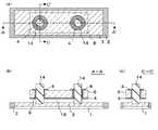
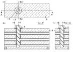
第2の実施形態の半導体装置は、第1の実施形態の半導体装置のSDを変更したものである。本発明の第2の実施形態を、図面を参照して以下に説明する。図20(a)(b)(c)は、それぞれ、本発明の第2の実施形態である半導体装置の断面図である。図20(a)(b)(c)は、それぞれ、図1の(c)に対応する断面図であり、これらの図により、第1の実施形態の半導体装置との違いを示す。図20(a)(b)(c)、いずれの場合でも、各半導体装置の上面図は、図1(a)と同じである。図1(b)に対応する断面図は、SDのみ、図20(a)(b)(c)に示すように変更される。なお、本実施形態の半導体装置は、n型MISFETであっても、p型MISFETであってもかまわない。ここでは、n型MISFETを一例として説明する。<Second Embodiment>
The semiconductor device of the second embodiment is obtained by changing the SD of the semiconductor device of the first embodiment. A second embodiment of the present invention will be described below with reference to the drawings. 20A, 20B, and 20C are cross-sectional views of a semiconductor device according to the second embodiment of the present invention. FIGS. 20A, 20B, and 20C are cross-sectional views corresponding to FIG. 1C, respectively, and show the differences from the semiconductor device of the first embodiment. 20A, 20B, and 20C, the top view of each semiconductor device is the same as FIG. The cross-sectional view corresponding to FIG. 1B is changed as shown in FIGS. 20A, 20B, and 20C only for SD. Note that the semiconductor device of this embodiment may be an n-type MISFET or a p-type MISFET. Here, an n-type MISFET will be described as an example.
図20(a)は、柱状半導体14の半径が、n型拡散層(不純物領域)19の深さよりも小さく、シリサイド18の厚みより大きい場合である。この場合、n型拡散層19は、柱状半導体14の横断面でみたときに柱状半導体の中心まで分布している。すなわち縦型MISFETのSD部において、pn接合界面が、チャネル領域と接する部分だけになる。このため、第1の実施形態の半導体装置に比べて、接合リーク電流が減少する。 FIG. 20A shows a case where the radius of the
図20(b)は、柱状半導体14の半径が、n型拡散層(不純物領域)19の深さよりも小さく、かつ、シリサイド18の厚みよりも小さい場合である。この場合、縦型MISFETのSD部において、半導体部分が減少し、チャネル領域に接する部分を除いて、すべてシリサイド18となる。すなわち柱状半導体14の横断面で見たときに、シリサイド18は柱状半導体14の中心まで形成されている。したがって、第1の実施形態の半導体装置に比べて、接合リーク電流が減少することに加え、さらにSD部の寄生抵抗が減少する。 FIG. 20B shows the case where the radius of the
図20(c)は、シリサイド18に接するn型拡散層(不純物領域)19が、すべて空乏化したn型拡散層(不純物領域)23になっている場合である。この場合、縦型MISFETのチャネル領域とSD部の境界がpn接合ではなく、ショットキー接合となり、縦型MISFETはショットキーSDトランジスタとなる。また、図20(a)(b)において、n型拡散層(不純物領域)19をすべて空乏化させて、ショットキーSDトランジスタとすることもできる。 FIG. 20C shows a case where the n-type diffusion layer (impurity region) 19 in contact with the
次に、本実施形態の半導体装置の製造方法について説明する。本実施形態の半導体装置の製造方法は、図20(a)(b)(c)のいずれも、第1の実施形態の半導体装置の製造方法と同じである。図20(a)(b)に示す半導体装置の条件を満たすためには、柱状半導体14の半径(もしくは断面積)を高解像度なリソグラフィ(例えば電子線リソグラフィ)を用いて小さくするか、もしくは、シリサイド18の厚みを厚くすればよい。シリサイド18の厚みを厚くするには、シリサイド18を全量反応で形成する場合、シリサイド金属17の成膜時の膜厚を厚くすればよい。図20(c)に示す半導体装置の条件を満たすためには、特許文献5(段落[0023]〜[0027])に記載されているような条件を満たすように、ドーピング濃度を調整する。 Next, a method for manufacturing the semiconductor device of this embodiment will be described. The semiconductor device manufacturing method according to the present embodiment is the same as the semiconductor device manufacturing method according to the first embodiment in FIGS. 20A, 20B, and 20C. In order to satisfy the conditions of the semiconductor device shown in FIGS. 20A and 20B, the radius (or cross-sectional area) of the
なお、図20(a)(b)(c)の各装置をp型MISFETにする場合の変更については、第1の実施形態と同様である。 Note that changes in the case where each device in FIGS. 20A, 20B, and 20C is made to be a p-type MISFET are the same as those in the first embodiment.
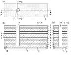
<第3の実施形態>
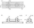
第3の実施形態の半導体装置は、第1の実施形態の半導体装置をCMOS(Complementary Metal Oxide Semiconductor)にしたものである。本発明の第3の実施形態を、図面を参照して以下に説明する。図21(a)は、本発明の第1の実施形態である半導体装置の上面図である。また、図21(b)は、図21(a)のA−A´線に沿った断面図、図21(c)は、図21(a)のC−C´線に沿った断面図である。<Third Embodiment>
The semiconductor device according to the third embodiment is obtained by replacing the semiconductor device according to the first embodiment with a CMOS (Complementary Metal Oxide Semiconductor). A third embodiment of the present invention will be described below with reference to the drawings. FIG. 21A is a top view of the semiconductor device according to the first embodiment of the present invention. 21B is a cross-sectional view taken along the line AA ′ in FIG. 21A, and FIG. 21C is a cross-sectional view taken along the line CC ′ in FIG. is there.
本実施形態の半導体装置では、図21(b)の左側の柱状半導体14がn型の縦型MISFET、右側の柱状半導体14がp型の縦型MISFETである。図21(b)は、n型とp型の縦型MISFETをそれぞれ1個ずつ用いて、インバータを形成した例を示している。双方のゲート電極は、シリサイド18同士、もしくは、コンタクト22を介した接触により、電気的に短絡されている。図21(b)左側、n型の縦型MISFETについては、第1の実施形態の半導体装置と同じである。図21(b)右側のp型の縦型MISFETは、図21(b)左側のn型の縦型MISFETのドーピングを変更したものである。以下にドーピングの変更箇所を説明する。 In the semiconductor device of this embodiment, the
まず、右側のp型の縦型MISFETは、半導体基板1上のp型拡散層(不純物領域)24に形成された柱状半導体14の側面に形成されている。柱状半導体14の上部、下部がSDとなっており、中央部がチャネル領域となっている。p型の縦型MISFETであるので、チャネル領域はn型にドーピングされている。また上部SDと下部SDは、シリサイド18に接して形成されたp型拡散層(不純物領域)25となっている。またゲート層6は、図21(b)の左半分がn型の縦型MISFET用にn型にドーピングされており、右半分がp型の縦型MISFET用にp型にドーピングされている。なお、本実施形態の半導体装置では、n型の縦型MISFETに形成されるシリサイドと、p型の縦型MISFETに形成されるシリサイドの種類は、同じであっても、異なっていてもよい。図21では、シリサイド18として同じ場合を示している。また、柱状半導体14の断面積や断面形状が、n型の縦型MISFETとp型の縦型MISFETとで同じであってもよいし、異なっていてもよい、図21では、これらの断面積及び断面形状が同じ場合を例示している。 First, the right p-type vertical MISFET is formed on the side surface of the
以下、図22から図31を用いて、本実施形態の半導体装置の製造方法の一例についてより詳細に説明する。図22から図31は、本実施形態の縦型MISFETの製造工程における各段階の状態の一例を示す模式図である。各図の(a)が上面図、各図の(b)が各図の(a)のA−A´線に沿った断面図、各図の(c)が各図の(a)のC−C´線に沿った断面図である。本実施形態の半導体装置の製造方法は、第1の実施形態の半導体装置の製造方法をもとに、デュアルシリサイドを形成できるように変更したものである。 Hereinafter, an example of the method for manufacturing the semiconductor device of the present embodiment will be described in more detail with reference to FIGS. FIG. 22 to FIG. 31 are schematic views showing an example of the state of each stage in the manufacturing process of the vertical MISFET of this embodiment. (A) of each figure is a top view, (b) of each figure is a cross-sectional view taken along the line AA 'of (a) of each figure, (c) of each figure is C of (a) of each figure. It is sectional drawing along a -C 'line. The manufacturing method of the semiconductor device of this embodiment is modified so that dual silicide can be formed based on the manufacturing method of the semiconductor device of the first embodiment.
まず、図22に示すように、半導体基板1に素子分離絶縁膜2を形成する。以下では、半導体基板1を、最も一般的なp型単結晶Si(100)基板として説明する。素子分離絶縁膜2の形成は、例えばSTI(Shallow Trench Isolation)法、または、LOCOS(Local Oxidation of Silicon)法を用いる。 First, as shown in FIG. 22, the element
次いで図23に示すように、半導体基板1にn型拡散層(不純物領域)3とp型拡散層(不純物領域)24を形成する。具体的には、レジスト塗布、露光、現像という一連のリソグラフィ工程を行って、n型の縦型MISFET部分(図中左側)にレジストが残らないようなレジストパターン(未図示)を半導体基板1の上に作製する。その後、このレジストパターンをマスクに、pウェル形成のため、p型のドーパント(Bなど)をイオン注入し、さらに、下部SD電極形成のため、n型のドーパント(P、Asなど)をイオン注入し、レジストを剥離する。それから、レジスト塗布、露光、現像という一連のリソグラフィ工程を行って、p型の縦型MISFET部分(図中右側)にレジストが残らないようなレジストパターン(未図示)を半導体基板1の上に作製する。その後、このレジストパターンをマスクに、nウェル形成のため、n型のドーパント(P、Asなど)をイオン注入し、さらに、下部SD電極形成のため、p型のドーパント(Bなど)をイオン注入し、レジストを剥離する。この後、スパイクアニールを行い、注入したドーパントを活性化させ、n型MISFETを作製する領域(図中左側)に、pウェル(未図示)およびn型拡散層(不純物領域)3を形成し、p型MISFETを作製する領域(図中右側)に、nウェル(未図示)およびp型拡散層(不純物領域)24を形成する。 Next, as shown in FIG. 23, an n-type diffusion layer (impurity region) 3 and a p-type diffusion layer (impurity region) 24 are formed in the
この後、第1の実施形態の半導体装置の製造方法において、図4から図15に示した工程を行う。 Thereafter, in the method of manufacturing the semiconductor device according to the first embodiment, the steps shown in FIGS. 4 to 15 are performed.
次いで図24に示すように、マスク絶縁膜26を成膜する。マスク絶縁膜26は、シリサイドを形成したくない領域を覆うためのものである。一般には、SW15と同じ種類の絶縁膜でよく、例えば、Si窒化膜とし、減圧CVDで成膜する。 Next, as shown in FIG. 24, a
次いで図25に示すように、n型の縦型MISFET部分(図中左側)の、マスク絶縁膜26、SW15、第2絶縁膜5を除去して、n型の縦型MISFETを形成する柱状半導体14の天面と側面、ゲート層6、半導体基板1上のn型拡散層(不純物領域)3を露出させる。具体的には、レジスト塗布、露光、現像という一連のリソグラフィ工程を行って、n型の縦型MISFET部分(図中左側)にレジストが残らないようなレジストパターン(未図示)を作製する。その後、このレジストパターンをマスクに、熱りん酸で、マスク絶縁膜26、SW15、第2絶縁膜5をウエットエッチングして除去する。その後、レジストを剥離する。レジストのウエットエッチング耐性が十分でない場合は、マスク絶縁膜26の成膜後、ハードマスクとして、マスク絶縁膜26とは種類が異なる絶縁膜を成膜する。成膜後、同様にリソグラフィを行い、得られたレジストパターンをマスクに、ハードマスクをエッチングする。そして、レジストを除去した後、ハードマスクをマスクにして、マスク絶縁膜26、SW15、第2絶縁膜5をウエットエッチングして除去する。その後、ハードマスクを除去する。 Next, as shown in FIG. 25, the columnar semiconductor forming the n-type vertical MISFET by removing the
次いで図26に示すように、第1の実施形態の図17、図18に示す工程を行って、シリサイド18を形成する。これにより、n型の縦型MISFETとなる柱状半導体14の天面と側面、ゲート層6、半導体基板1上のn型拡散層(不純物領域)3に、シリサイド18が形成される。また、n型の縦型MISFETのSDとなる、n型拡散層(不純物領域)19が、柱状半導体14に形成されたシリサイド18に接して形成される。 Next, as shown in FIG. 26, the steps shown in FIGS. 17 and 18 of the first embodiment are performed to form the
次いで図27に示すように、p型の縦型MISFET部分(図中右側)の、マスク絶縁膜26、SW15、第2絶縁膜5を除去する。例えば、熱りん酸でウエットエッチングする。この後、図28に示すように、再度、マスク絶縁膜26を成膜する。例えば、Si窒化膜とし、減圧CVDで成膜する。 Next, as shown in FIG. 27, the
次いで図29に示すように、p型の縦型MISFET部分(図中右側)の、マスク絶縁膜26、SW15、第2絶縁膜5を除去して、p型の縦型MISFETを形成する柱状半導体14の天面と側面、ゲート層6、半導体基板1上のp型拡散層(不純物領域)24を露出させる。具体的には、レジスト塗布、露光、現像という一連のリソグラフィ工程を行って、p型の縦型MISFET部分(図中右側)にレジストが残らないようなレジストパターン(未図示)を作製する。その後、このレジストパターンをマスクに、熱りん酸で、マスク絶縁膜26、SW15、第2絶縁膜5をウエットエッチングして除去する。その後、レジストを剥離する。レジストのウエットエッチング耐性が十分でない場合は、マスク絶縁膜26の成膜後、ハードマスクとして、マスク絶縁膜26とは種類が異なる絶縁膜を成膜する。成膜後、同様にリソグラフィを行い、得られたレジストパターンをマスクに、ハードマスクをエッチングする。そして、レジストを除去した後、ハードマスクをマスクにして、マスク絶縁膜26、SW15、第2絶縁膜5をウエットエッチングして除去する。その後、ハードマスクを除去する。 Next, as shown in FIG. 29, the columnar semiconductor forming the p-type vertical MISFET by removing the
次いで図30に示すように、第1の実施形態の図17、図18に示す工程を行って、シリサイド18を形成する。ただし、図17に示す工程において、気相ドーピングは、B2H6を使用して行う。これにより、p型の縦型MISFETとなる柱状半導体14の天面と側面、ゲート層6、半導体基板1上のp型拡散層(不純物領域)24に、シリサイド18が形成される。また、p型の縦型MISFETのSDとなる、p型拡散層(不純物領域)25が、柱状半導体14に形成されたシリサイド18に接して形成される。Next, as shown in FIG. 30, the
次いで図31に示すように、n型の縦型MISFET部分(図中左側)の、マスク絶縁膜26を除去する。例えば、熱りん酸でウエットエッチングする。 Next, as shown in FIG. 31, the
この後、第1の実施形態の図19に示す工程から後の工程を同様に行うと、図21に示す半導体装置が完成する。なお上記の例では、n型の縦型MISFET、p型の縦型MISFETの順にシリサイドを形成したが、順番に制限はなく、逆でもよい。 Thereafter, when the steps after the step shown in FIG. 19 of the first embodiment are similarly performed, the semiconductor device shown in FIG. 21 is completed. In the above example, the silicide is formed in the order of the n-type vertical MISFET and the p-type vertical MISFET, but the order is not limited and may be reversed.
またn型の縦型MISFETとp型の縦型MISFETで、シリサイドの種類を変えるときは、図30に示す工程で、n型の縦型MISFETに形成したシリサイドと異なる種類のシリサイドを形成する。シリサイドの種類が異なる場合は、耐熱性の高いシリサイドを先に形成し、耐熱性の劣るシリサイドを後に形成するのがよい。 When the type of silicide is changed between the n-type vertical MISFET and the p-type vertical MISFET, silicide of a different type from the silicide formed on the n-type vertical MISFET is formed in the step shown in FIG. When the type of silicide is different, it is preferable to form a silicide with high heat resistance first and form a silicide with poor heat resistance later.
また、上記の例では、図27に示す工程で、p型の縦型MISFET部分(図中右側)の、マスク絶縁膜26、SW15、第2絶縁膜5を除去したが、これを行わず、図28に示す工程に進み、マスク絶縁膜26を成膜してもよい。この場合、図29に示す工程で、マスク絶縁膜26、SW15、第2絶縁膜5を除去する。さらに、上記の例では、図31に示す工程で、n型の縦型MISFET部分(図中左側)の、マスク絶縁膜26を除去したが、これを行わず、次工程に進んでも良い。この場合、コンタクトホールを形成するドライエッチング時に、n型の縦型MISFET部分(図中左側)では、層間絶縁膜21、ストッパー絶縁膜20に加えて、マスク絶縁膜26をエッチングすることになる。 In the above example, in the step shown in FIG. 27, the
<第4の実施形態>
第4の実施形態の半導体装置は、第1の実施形態の半導体装置を積層したものである。本発明の第4の実施形態の半導体装置を、図面を参照して以下に説明する。<Fourth Embodiment>
The semiconductor device of the fourth embodiment is obtained by stacking the semiconductor devices of the first embodiment. A semiconductor device according to a fourth embodiment of the present invention will be described below with reference to the drawings.
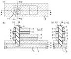
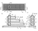
図32(a)は、本発明の第4の実施形態である半導体装置の上面図である。また、図32(b)は、図32(a)のA−A´線に沿った断面図、図32(c)は、図32(a)のC−C´線に沿った断面図である。本実施形態の半導体装置は、n型MISFETであっても、p型MISFETであってもかまわない。ここでは、n型MISFETを一例として説明する。 FIG. 32A is a top view of the semiconductor device according to the fourth embodiment of the present invention. 32B is a cross-sectional view taken along the line AA ′ in FIG. 32A, and FIG. 32C is a cross-sectional view taken along the line CC ′ in FIG. is there. The semiconductor device of this embodiment may be an n-type MISFET or a p-type MISFET. Here, an n-type MISFET will be described as an example.
図32に示す半導体装置は、図1に示す半導体装置を積層したものである。ただし、図1では、柱状半導体14を2個図示していたのに対し、図32では1個図示している。本実施形態の半導体装置では、半導体基板1または半導体層にn型拡散層(不純物領域)3が形成され、n型拡散層(不純物領域)3は、その周囲を素子分離絶縁膜2に囲まれている。また、n型拡散層(不純物領域)3の上には、柱状半導体14が形成されている。柱状半導体14には、複数個、例えば3つの縦型MISFETが形成され、それらが直列に接続した形となっている。柱状半導体14には、その周囲を囲むように、ゲート絶縁膜9が高さ方向に例えば3箇所形成され、さらに、各ゲート絶縁膜9の周囲を囲むように、ゲート層6が例えば3つ形成されている。それぞれのゲート層6の上下には、第1絶縁膜4が形成され、第1絶縁膜4は、柱状半導体14にも接している。なお図32では、第1の実施形態における図1のように、第1絶縁膜4は柱状半導体14に接しているが、第1の実施形態における図43のように、ゲート絶縁膜9の製造方法によっては、第1絶縁膜4は柱状半導体14に接していない場合もある。また各ゲート層6は、そのゲート層6より上に位置するゲート層6から平面視ではみ出した部分を有しており、このはみ出した部分でコンタクト22に接続している。 The semiconductor device shown in FIG. 32 is obtained by stacking the semiconductor devices shown in FIG. However, while FIG. 1 shows two
柱状半導体14の側面には、第1絶縁膜4によって、セルフ・アラインされた位置に、シリサイド18が形成され、シリサイド18に接して、n型拡散層(不純物領域)19が形成されている。このn型拡散層(不純物領域)19は、それぞれの縦型MISFETの上部SD電極、および下部SD電極となる。一番上の縦型MISFETの上側の第1絶縁膜4によって、セルフ・アラインされた位置に形成されたシリサイド18は、柱状半導体14の天面まで連続してつながっている。柱状半導体14の天面に形成されたシリサイド18には、コンタクト22が層間絶縁膜21、ストッパー絶縁膜20を貫く形で接続している。また一番下の縦型MISFETの下側の第1絶縁膜4によって、セルフ・アラインされた位置に形成されたシリサイド18は、半導体基板1上のn型拡散層(不純物領域)3まで連続してつながっている。n型拡散層(不純物領域)3に形成されたシリサイド18には、コンタクト22が層間絶縁膜21、ストッパー絶縁膜20を貫く形で接続している。シリサイド18は、3つのゲート層6の上面、および側面にも形成されている。ゲート層6の上面に形成されたシリサイド18には、コンタクト22が層間絶縁膜21、ストッパー絶縁膜20を貫く形で接続している。 On the side surface of the
なお図32に示す半導体装置は、1つの柱状半導体に縦型MIEFETが3個直列接続されているが、これはあくまで例であり、縦型MISFETの積層数は任意である。 In the semiconductor device shown in FIG. 32, three vertical MIEFETs are connected in series to one columnar semiconductor, but this is only an example, and the number of stacked vertical MISFETs is arbitrary.
半導体基板1、柱状半導体14、ゲート絶縁膜9、シリサイド18、n型拡散層(不純物領域)19については、第1の実施形態の半導体装置と同様である。第1絶縁膜4とゲート層6の膜厚は、積層する各縦型MISFETで異なっていてよい。特に、プレーナー型MISFETのSWでは、各MISFETでSW幅を容易に変えられないのに対し、本発明の半導体装置では、各縦型MISFETで第1絶縁膜4の膜厚を変更できる点が大きな特徴である。また各縦型MISFETのシリサイド18の長さも任意に変更できる。 The
以下、図33から図42を用いて、本実施形態の半導体装置の製造方法の一例についてより詳細に説明する。図33から図42は、本実施形態の縦型MISFETの製造工程における各段階の状態の一例を示す模式図である。各図の(a)が上面図、各図の(b)が各図の(a)のA−A´線に沿った断面図、各図の(c)が各図の(a)のC−C´線に沿った断面図である。本実施形態の製造方法は、n型MISFETにも、p型MISFETにも適用可能である。ここでは、n型MISFETの製造方法を一例として説明する。 Hereinafter, an example of the method for manufacturing the semiconductor device of the present embodiment will be described in more detail with reference to FIGS. FIG. 33 to FIG. 42 are schematic views showing an example of the state of each stage in the manufacturing process of the vertical MISFET of this embodiment. (A) of each figure is a top view, (b) of each figure is a cross-sectional view taken along the line AA 'of (a) of each figure, (c) of each figure is C of (a) of each figure. It is sectional drawing along a -C 'line. The manufacturing method of the present embodiment can be applied to an n-type MISFET and a p-type MISFET. Here, an n-type MISFET manufacturing method will be described as an example.
まず、第1の実施形態の半導体装置の製造方法において図2から図3に示した工程と同様な工程を行う。 First, steps similar to those shown in FIGS. 2 to 3 are performed in the semiconductor device manufacturing method of the first embodiment.
次いで図33に示すように、半導体基板1のn型拡散層(不純物領域)3上に、第2絶縁膜5、第1絶縁膜4、ゲート層6、第1絶縁膜4、第2絶縁膜5、第1絶縁膜4、ゲート層6、第1絶縁膜4、第2絶縁膜5、第1絶縁膜4、ゲート層6、第1絶縁膜4、第2絶縁膜5を、この順に成膜する。例えば、第2絶縁膜5をSi窒化膜、第1絶縁膜4をSi酸化膜、ゲート層6を多結晶Siとして、いずれも減圧CVDで成膜する。 Next, as shown in FIG. 33, the second
次いで図34に示すように、これらの積層膜を貫き、半導体基板1のn型拡散層(不純物領域)3にいたる開口7を形成する。具体的には、最上層の第2絶縁膜5の成膜後、レジスト塗布、露光、現像という一連のリソグラフィ工程を行って、所望の開口部分のレジストが残らないようなレジストパターン(未図示)を第2絶縁膜5の上に作製する。その後、このレジストパターンをマスクに、第2絶縁膜5、第1絶縁膜4、ゲート層6、第1絶縁膜4、第2絶縁膜5、第1絶縁膜4、ゲート層6、第1絶縁膜4、第2絶縁膜5、第1絶縁膜4、ゲート層6、第1絶縁膜4、第2絶縁膜5を順にドライエッチングし、n型拡散層(不純物領域)3にいたる開口7を形成する。エッチング後、レジスト(未図示)を剥離すると、図33に示す形状が得られる。なお、開口7の断面形状や断面積については、第1の実施形態の半導体装置の製造方法と同じである。 Next, as shown in FIG. 34, an
その後、第1の実施形態の半導体装置の製造方法において、図6から図11に示す工程と同様な工程を行う。そうすると、図35のような形状が得られる。すなわち、開口7に単結晶からなる柱状半導体14が形成され、各ゲート層6と柱状半導体14の間には、ゲート絶縁膜9が形成される。 Thereafter, in the method for manufacturing the semiconductor device of the first embodiment, steps similar to those shown in FIGS. 6 to 11 are performed. Then, a shape as shown in FIG. 35 is obtained. That is, a
次いで、第1の実施形態の半導体装置の製造方法において、図12から図14に示す工程と同様な工程を行う。そうすると、図36のような形状が得られる。すなわち、柱状半導体14の上部にSW15が形成され、ゲート層6のうち、最も上にあるゲート層6が露出される。 Next, in the method for manufacturing the semiconductor device of the first embodiment, steps similar to those shown in FIGS. 12 to 14 are performed. Then, a shape as shown in FIG. 36 is obtained. That is, the
次いで図37に示すように、ゲート層6のうち、最も上にあるゲート層6のパターンニングを行う。具体的には、レジスト塗布、露光、現像という一連のリソグラフィ工程を行って、最も上にあるゲート層6のパターンが残るようなレジストパターン(未図示)を作製する。次いで、このレジストパターンをマスクに、ゲート層6、第1絶縁膜4、第2絶縁膜5、第1絶縁膜4を順にドライエッチングし、真ん中のゲート層6でエッチングを停止させる。エッチング後、レジストパターン(未図示)を剥離する。 Next, as shown in FIG. 37, the
次いで図38に示すように、ゲート層6のうち、真ん中のゲート層6のパターンニングを行う。具体的には、レジスト塗布、露光、現像という一連のリソグラフィ工程を行って、真ん中のゲート層6のパターンが残るようなレジストパターン(未図示)を作製する。それから、このレジストパターンをマスクに、ゲート層6、第1絶縁膜4、第2絶縁膜5、第1絶縁膜4を順にドライエッチングし、最も下にあるゲート層6でエッチングを停止させる。エッチング後、レジストパターン(未図示)を剥離する。なお、このとき、リソグラフィは、理想的に位置ずれ0で行えると仮定して、図38を図示している。 Next, as shown in FIG. 38, the
次いで図39に示すように、ゲート層6のうち、最も下にあるゲート層6のパターンニングを行う。具体的には、レジスト塗布、露光、現像という一連のリソグラフィ工程を行って、最も下のゲート層6のパターンが残るようなレジストパターン(未図示)を作製する。それから、このレジストパターンをマスクに、ゲート層6、第1絶縁膜4、第2絶縁膜5を順にドライエッチングし、半導体基板1上のn型拡散層(不純物領域)3で停止させる。エッチング後、レジストパターン(未図示)を剥離する。なお、このときも、リソグラフィは、理想的に位置ずれ0で行えると仮定して、図39を図示している。 Next, as shown in FIG. 39, patterning is performed on the
この後、第1の実施形態の半導体装置の製造方法の図16に示す工程と同様にして、SW15、第2絶縁膜5を除去すると、図40に示すように、柱状半導体14の側面が露出される。 Thereafter, when the
柱状半導体14の側面を露出させた後、第1の実施形態の半導体装置の製造方法において、図17から図18に示す工程と同様な工程を行う。そうすると、図41に示すように、柱状半導体14の天面、側面、各ゲート層の上面、側面、半導体基板1のn型拡散層(不純物領域)3に、シリサイド18が形成される。また、柱状半導体14の側面に形成されたシリサイド18に接して、n型拡散層(不純物領域)19が形成される。 After the side surfaces of the
次いで図42に示すように、ストッパー絶縁膜20と層間絶縁膜21をこの順にCVDで形成し、層間絶縁膜21の表面をCMPで平坦化する。 Next, as shown in FIG. 42, the
この後、従来からの技術を用いて、コンタクト22を形成する。例えば、レジスト塗布、露光、現像という一連のリソグラフィ工程を行って、コンタクトを形成する部分にレジストが残らないようなレジストパターン(未図示)を作製する。その後、このレジストパターンをマスクに、層間絶縁膜21、ストッパー絶縁膜20を順にドライエッチングする。エッチング後、レジスト(未図示)を剥離する。さらにTiとTiNをスパッタして熱処理し、その後、CVDによりWを埋め込んで、CMPを行う。このようにして、図32のような半導体装置が完成する。その後、必要に応じて、従来からの方法で配線層や電極パッドがさらに形成される。 Thereafter,
なお、上記の例では、n型MISFETを例に説明したが、p型MISFETへの変更は、第1の実施形態の場合と同様である。また、PSG、BSGを用いて、シリサイド金属17の成膜前にSDを形成しておくことも、第1の実施形態の場合と同様に可能である。 In the above example, the n-type MISFET is described as an example. However, the change to the p-type MISFET is the same as that in the first embodiment. Further, it is possible to form the SD using PSG and BSG before forming the
以上、図面を参照して本発明の実施形態について述べたが、これらは本発明の例示であり、上記以外の様々な構成を採用することもできる。 As mentioned above, although embodiment of this invention was described with reference to drawings, these are the illustrations of this invention, Various structures other than the above are also employable.
1 半導体基板
2 素子分離絶縁膜
3 n型拡散層
4 絶縁膜
5 絶縁膜
6 ゲート層
7 開口
8 開口
9 ゲート絶縁膜
10 絶縁膜
11 CVDゲート絶縁膜
12 側壁
13 柱状半導体
14 柱状半導体
15 SW
16 空隙
17 シリサイド金属
18 シリサイド
19 n型拡散層
20 ストッパー絶縁膜
21 層間絶縁膜
22 コンタクト
23 n型拡散層
24 p型拡散層
25 p型拡散層
26 マスク絶縁膜DESCRIPTION OF
16
Claims (19)
Translated fromJapanese前記柱状半導体の側面の一部に接するゲート絶縁膜と、
前記ゲート絶縁膜のうち前記柱状半導体とは逆側の面に接するゲートと、
前記ゲートの上及び下それぞれに形成され、前記ゲート及び前記ゲート絶縁膜に接している第1絶縁膜と、
前記柱状半導体の前記側面のうち、前記ゲートに面する領域より上側の領域及び下側の領域それぞれに形成されており、前記柱状半導体の前記側面のうち前記第1絶縁膜に対向する領域に接しているシリサイドと、
を備える半導体装置。Columnar semiconductors,
A gate insulating film in contact with a part of the side surface of the columnar semiconductor;
A gate in contact with a surface of the gate insulating film opposite to the columnar semiconductor;
A first insulating film formed on and under the gate, and in contact with the gate and the gate insulating film;
Of the side surface of the columnar semiconductor, formed on each of a region above and below a region facing the gate, and is in contact with a region of the side surface of the columnar semiconductor facing the first insulating film. With silicide,
A semiconductor device comprising:
前記第1絶縁膜は、前記柱状半導体の前記側面のうち前記ゲート絶縁膜に接する領域の上及び下それぞれに形成され、
前記シリサイドは、前記柱状半導体の前記側面のうち前記第1絶縁膜及び前記ゲート絶縁膜に覆われていない領域に形成されている半導体装置。The semiconductor device according to claim 1,
The first insulating film is formed above and below a region of the side surface of the columnar semiconductor that is in contact with the gate insulating film,
The silicide is a semiconductor device formed in a region of the side surface of the columnar semiconductor that is not covered with the first insulating film and the gate insulating film.
前記ゲート及び2つの前記第1絶縁膜は、いずれも前記ゲート絶縁膜を介して前記柱状半導体の前記側面に面しており、
前記シリサイドは、前記柱状半導体の前記側面のうち前記ゲート絶縁膜に覆われていない領域に形成されている半導体装置。The semiconductor device according to claim 1,
Each of the gate and the two first insulating films faces the side surface of the columnar semiconductor via the gate insulating film,
The silicide is a semiconductor device formed in a region of the side surface of the columnar semiconductor that is not covered with the gate insulating film.
前記ゲート絶縁膜より上に位置する前記シリサイドは、前記柱状半導体の前記側面及び天面に連続的に形成されている半導体装置。The semiconductor device according to claim 2 or 3,
The semiconductor device, wherein the silicide located above the gate insulating film is continuously formed on the side surface and the top surface of the columnar semiconductor.
前記柱状半導体は半導体層または半導体基板の上に形成されており、
前記ゲート絶縁膜より下に位置する前記シリサイドは、前記柱状半導体の前記側面及び前記半導体層または半導体基板の表面のうち前記柱状半導体の周囲に位置する領域に連続的に形成されている半導体装置。In the semiconductor device according to any one of claims 2 to 4,
The columnar semiconductor is formed on a semiconductor layer or a semiconductor substrate,
The said silicide located below the said gate insulating film is a semiconductor device continuously formed in the area | region located in the circumference | surroundings of the said columnar semiconductor among the said side surface of the said columnar semiconductor, and the surface of the said semiconductor layer or a semiconductor substrate.
前記柱状半導体のうち前記ゲート絶縁膜に接する領域にはチャネル不純物が導入されており、
前記柱状半導体のうち前記シリサイドが形成されている部分に形成され、前記柱状半導体の横断面でみたときに前記柱状半導体の中心まで分布している、前記チャネル不純物とは異なる導電型の不純物領域を備える半導体装置。In the semiconductor device according to any one of claims 1 to 5,
A channel impurity is introduced into a region in contact with the gate insulating film in the columnar semiconductor,
An impurity region having a conductivity type different from that of the channel impurity, which is formed in a portion of the columnar semiconductor where the silicide is formed and is distributed to the center of the columnar semiconductor when viewed in a cross section of the columnar semiconductor. A semiconductor device provided.
前記柱状半導体の横断面でみたときに、前記シリサイドは前記柱状半導体の中心まで形成されている半導体装置。In the semiconductor device according to any one of claims 1 to 5,
The semiconductor device, wherein the silicide is formed up to a center of the columnar semiconductor when viewed in a cross section of the columnar semiconductor.
上側に位置する前記第1絶縁膜と、下側に位置する前記第1絶縁膜の厚さは、互いに異なる半導体装置。In the semiconductor device according to any one of claims 1 to 7,
The thickness of the first insulating film located on the upper side and the thickness of the first insulating film located on the lower side are different semiconductor devices.
前記柱状半導体のうち前記ゲート絶縁膜に接するチャネル領域にはチャネル不純物が導入されており、
前記柱状半導体のうち前記シリサイドと接する領域に形成されている、前記チャネル不純物とは異なる導電型の不純物領域を備え、
前記不純物領域は完全に空乏化しており、前記チャネル領域の間でショットキー接合を形成している半導体装置。In the semiconductor device according to any one of claims 1 to 8,
A channel impurity is introduced into a channel region in contact with the gate insulating film in the columnar semiconductor,
An impurity region of a conductivity type different from the channel impurity, formed in a region of the columnar semiconductor in contact with the silicide;
The semiconductor device in which the impurity region is completely depleted and a Schottky junction is formed between the channel regions.
前記柱状半導体、前記ゲート絶縁膜、前記ゲート、前記第1絶縁膜、及び前記シリサイドを有するトランジスタを、前記柱状半導体が互いに重なるように複数重ねて有する半導体装置。The semiconductor device according to any one of claims 1 to 9,
A semiconductor device including a plurality of transistors each including the columnar semiconductor, the gate insulating film, the gate, the first insulating film, and the silicide so that the columnar semiconductors overlap each other.
前記柱状半導体、前記ゲート絶縁膜、前記ゲート、前記第1絶縁膜、及び前記シリサイドを有するトランジスタを、同一層に複数有する半導体装置。In the semiconductor device according to any one of claims 1 to 10,
A semiconductor device including a plurality of transistors each including the columnar semiconductor, the gate insulating film, the gate, the first insulating film, and the silicide in the same layer.
p型の前記トランジスタと、n型の前記トランジスタとを有する半導体装置。The semiconductor device according to claim 11,
A semiconductor device including the p-type transistor and the n-type transistor.
前記ゲート絶縁膜は、酸化シリコン膜と窒化シリコン膜の積層膜である半導体装置。The semiconductor device according to any one of claims 1 to 12,
The gate insulating film is a semiconductor device which is a laminated film of a silicon oxide film and a silicon nitride film.
前記柱状半導体の側面のうち前記第1の第1絶縁膜、前記ゲート層、及び前記第2の第1絶縁膜に面していない領域に金属層を形成する第2工程と、
熱処理を行うことにより、前記金属層と前記柱状半導体とを反応させてシリサイドを形成する第3工程と、
を備える半導体装置の製造方法。A columnar semiconductor, and a first stacked structure including a first first insulating film, a gate layer, and a second first insulating film facing a region apart from the upper end and the lower end of the side surfaces of the columnar semiconductor Forming a first step;
Forming a metal layer in a region of the side surface of the columnar semiconductor that does not face the first first insulating film, the gate layer, and the second first insulating film;
A third step of forming silicide by reacting the metal layer and the columnar semiconductor by performing heat treatment;
A method for manufacturing a semiconductor device comprising:
前記第1工程は、
半導体基板または半導体層上に第1の第2絶縁膜を形成する工程と、
第1の前記第2絶縁膜上に、前記第1の積層構造の上に第2の第2絶縁膜を積層した第2の積層構造を一つ、または繰り返し形成することにより、第3の積層構造を形成する工程と、
前記第3の積層構造に前記柱状半導体を埋め込む工程と、
前記第1の第2絶縁膜及び前記第2の第2絶縁膜を除去する工程と、
を備える半導体装置の製造方法。In the manufacturing method of the semiconductor device according to claim 14,
The first step includes
Forming a first second insulating film on a semiconductor substrate or semiconductor layer;
A third laminated structure is formed by repeatedly or repeatedly forming a second laminated structure in which a second second insulating film is laminated on the first laminated structure on the first second insulating film. Forming a structure;
Embedding the columnar semiconductor in the third stacked structure;
Removing the first second insulating film and the second second insulating film;
A method for manufacturing a semiconductor device comprising:
前記第2工程において、前記金属層に不純物を含ませておき、
前記第3工程において、前記不純物を前記柱状半導体に拡散させる半導体装置の製造方法。In the manufacturing method of the semiconductor device according to claim 14 or 15,
In the second step, impurities are included in the metal layer,
A method of manufacturing a semiconductor device, wherein the impurity is diffused in the columnar semiconductor in the third step.
前記金属層を、不純物ガスを用いたCVD法により形成する半導体装置の製造方法。In the manufacturing method of the semiconductor device according to claim 16,
A method of manufacturing a semiconductor device, wherein the metal layer is formed by a CVD method using an impurity gas.
前記金属層をCVD法により形成する半導体装置の製造方法。In the manufacturing method of the semiconductor device according to claim 14 or 15,
A method of manufacturing a semiconductor device, wherein the metal layer is formed by a CVD method.
第1の前記柱状半導体を用いてn型トランジスタを形成すると共に、第2の前記柱状半導体を用いてp型トランジスタを形成する半導体装置の製造方法。
In the manufacturing method of the semiconductor device according to any one of claims 14 to 18,
A method for manufacturing a semiconductor device, wherein an n-type transistor is formed using the first columnar semiconductor and a p-type transistor is formed using the second columnar semiconductor.
Priority Applications (1)
| Application Number | Priority Date | Filing Date | Title |
|---|---|---|---|
| JP2010140330AJP2012004473A (en) | 2010-06-21 | 2010-06-21 | Semiconductor device and method for manufacturing semiconductor device |
Applications Claiming Priority (1)
| Application Number | Priority Date | Filing Date | Title |
|---|---|---|---|
| JP2010140330AJP2012004473A (en) | 2010-06-21 | 2010-06-21 | Semiconductor device and method for manufacturing semiconductor device |
Publications (1)
| Publication Number | Publication Date |
|---|---|
| JP2012004473Atrue JP2012004473A (en) | 2012-01-05 |
Family
ID=45536084
Family Applications (1)
| Application Number | Title | Priority Date | Filing Date |
|---|---|---|---|
| JP2010140330APendingJP2012004473A (en) | 2010-06-21 | 2010-06-21 | Semiconductor device and method for manufacturing semiconductor device |
Country Status (1)
| Country | Link |
|---|---|
| JP (1) | JP2012004473A (en) |
Cited By (19)
| Publication number | Priority date | Publication date | Assignee | Title |
|---|---|---|---|---|
| JP2013161978A (en)* | 2012-02-06 | 2013-08-19 | National Institute Of Advanced Industrial & Technology | Semiconductor storage device and manufacturing method of the same |
| JP2013175605A (en)* | 2012-02-24 | 2013-09-05 | Toshiba Corp | Manufacturing method for nonvolatile semiconductor memory device and nonvolatile semiconductor memory device |
| WO2014115305A1 (en)* | 2013-01-25 | 2014-07-31 | ユニサンティス エレクトロニクス シンガポール プライベート リミテッド | Semiconductor device |
| WO2014136728A1 (en)* | 2013-03-05 | 2014-09-12 | ピーエスフォー ルクスコ エスエイアールエル | Semiconductor device and manufacturing method therefor |
| WO2014170949A1 (en)* | 2013-04-16 | 2014-10-23 | ユニサンティス エレクトロニクス シンガポール プライベート リミテッド | Method for producing semiconductor device, and semiconductor device |
| JP2015084441A (en)* | 2014-12-17 | 2015-04-30 | ユニサンティス エレクトロニクス シンガポール プライベート リミテッドUnisantis Electronics Singapore Pte Ltd. | Semiconductor device |
| US9024376B2 (en) | 2013-01-25 | 2015-05-05 | Unisantis Electronics Singapore Pte. Ltd. | Vertical transistor with dielectrically-isolated work-function metal electrodes surrounding the semiconductor pillar |
| JP5740535B1 (en)* | 2013-07-19 | 2015-06-24 | ユニサンティス エレクトロニクス シンガポール プライベート リミテッドUnisantis Electronics Singapore Pte Ltd. | Semiconductor device manufacturing method and semiconductor device |
| JP2015159320A (en)* | 2015-04-27 | 2015-09-03 | ユニサンティス エレクトロニクス シンガポール プライベート リミテッドUnisantis Electronics Singapore Pte Ltd. | Semiconductor device manufacturing method and semiconductor device |
| JP5841696B1 (en)* | 2014-11-27 | 2016-01-13 | ユニサンティス エレクトロニクス シンガポール プライベート リミテッドUnisantis Electronics Singapore Pte Ltd. | Columnar semiconductor device and manufacturing method thereof |
| US9721957B2 (en) | 2013-12-20 | 2017-08-01 | Samsung Electronics Co., Ltd. | Static random access memory (SRAM) cells including vertical channel transistors |
| KR20170108912A (en)* | 2015-02-13 | 2017-09-27 | 타이완 세미콘덕터 매뉴팩쳐링 컴퍼니 리미티드 | Vertical gate all around (vgaa) devices and methods of manufacturing the same |
| US9876030B1 (en) | 2016-08-24 | 2018-01-23 | Toshiba Memory Corporation | Semiconductor device and method for manufacturing same |
| US10211339B2 (en) | 2016-03-21 | 2019-02-19 | Samsung Electronics Co., Ltd. | Vertical transistor having a semiconductor pillar penetrating a silicide formed on the substrate surface |
| US10559685B2 (en) | 2018-06-13 | 2020-02-11 | International Business Machines Corporation | Vertical field effect transistor with reduced external resistance |
| JP2021158368A (en)* | 2015-05-26 | 2021-10-07 | 株式会社半導体エネルギー研究所 | Semiconductor device |
| JP2022519537A (en)* | 2019-02-11 | 2022-03-24 | サンライズ メモリー コーポレイション | Applied memory circuit method as a bit line connector for a vertical thin film transistor and a vertical thin film transistor for a three-dimensional memory array. |
| JP2023038897A (en)* | 2021-09-07 | 2023-03-17 | 旺宏電子股▲ふん▼有限公司 | Three-dimensional semiconductor structures |
| JPWO2023067678A1 (en)* | 2021-10-19 | 2023-04-27 |
- 2010
- 2010-06-21JPJP2010140330Apatent/JP2012004473A/enactivePending
Cited By (44)
| Publication number | Priority date | Publication date | Assignee | Title |
|---|---|---|---|---|
| JP2013161978A (en)* | 2012-02-06 | 2013-08-19 | National Institute Of Advanced Industrial & Technology | Semiconductor storage device and manufacturing method of the same |
| JP2013175605A (en)* | 2012-02-24 | 2013-09-05 | Toshiba Corp | Manufacturing method for nonvolatile semiconductor memory device and nonvolatile semiconductor memory device |
| US9024376B2 (en) | 2013-01-25 | 2015-05-05 | Unisantis Electronics Singapore Pte. Ltd. | Vertical transistor with dielectrically-isolated work-function metal electrodes surrounding the semiconductor pillar |
| WO2014115305A1 (en)* | 2013-01-25 | 2014-07-31 | ユニサンティス エレクトロニクス シンガポール プライベート リミテッド | Semiconductor device |
| US9837503B2 (en) | 2013-01-25 | 2017-12-05 | Unisantis Electronics Singapore Pte. Ltd. | Transistor having metal electrodes surrounding a semiconductor pillar body and corresponding work-function-induced source/drain regions |
| US9496360B2 (en) | 2013-01-25 | 2016-11-15 | Unisantis Electronics Singapore Pte. Ltd. | Vertical transistor with source/drain regions induced by work-function differences between a semiconductor pillar body and surrounding metal electrodes |
| JP5670605B2 (en)* | 2013-01-25 | 2015-02-18 | ユニサンティス エレクトロニクス シンガポール プライベート リミテッドUnisantis Electronics Singapore Pte Ltd. | Semiconductor device |
| WO2014136728A1 (en)* | 2013-03-05 | 2014-09-12 | ピーエスフォー ルクスコ エスエイアールエル | Semiconductor device and manufacturing method therefor |
| WO2014170949A1 (en)* | 2013-04-16 | 2014-10-23 | ユニサンティス エレクトロニクス シンガポール プライベート リミテッド | Method for producing semiconductor device, and semiconductor device |
| US10002963B2 (en) | 2013-04-16 | 2018-06-19 | Unisantis Electronics Singapore Pte. Ltd. | Semiconductor device |
| US10056483B2 (en) | 2013-04-16 | 2018-08-21 | Unisantis Electronics Singapore Pte. Ltd. | Method for producing a semiconductor device including semiconductor pillar and fin |
| JP5654184B1 (en)* | 2013-04-16 | 2015-01-14 | ユニサンティス エレクトロニクス シンガポール プライベート リミテッドUnisantis Electronics Singapore Pte Ltd. | Semiconductor device manufacturing method and semiconductor device |
| US9768294B2 (en) | 2013-04-16 | 2017-09-19 | Unisantis Electronics Singapore Pte. Ltd. | Method for producing semiconductor device and semiconductor device |
| JP5740535B1 (en)* | 2013-07-19 | 2015-06-24 | ユニサンティス エレクトロニクス シンガポール プライベート リミテッドUnisantis Electronics Singapore Pte Ltd. | Semiconductor device manufacturing method and semiconductor device |
| US9997523B2 (en) | 2013-12-20 | 2018-06-12 | Samsung Electronics Co., Ltd. | Static random access memory (SRAM) cells including vertical channel transistors and methods of forming the same |
| US9721957B2 (en) | 2013-12-20 | 2017-08-01 | Samsung Electronics Co., Ltd. | Static random access memory (SRAM) cells including vertical channel transistors |
| JP5841696B1 (en)* | 2014-11-27 | 2016-01-13 | ユニサンティス エレクトロニクス シンガポール プライベート リミテッドUnisantis Electronics Singapore Pte Ltd. | Columnar semiconductor device and manufacturing method thereof |
| WO2016084205A1 (en)* | 2014-11-27 | 2016-06-02 | ユニサンティス エレクトロニクス シンガポール プライベート リミテッド | Columnar semiconductor device and method for manufacturing same |
| US9673321B2 (en) | 2014-11-27 | 2017-06-06 | Unisantis Electronics Singapore Pte. Ltd. | Pillar-shaped semiconductor device and method for producing the same |
| US10050124B2 (en) | 2014-11-27 | 2018-08-14 | Unisantis Electronics Singapore Pte. Ltd. | Method for producing a pillar-shaped semiconductor device |
| JP2015084441A (en)* | 2014-12-17 | 2015-04-30 | ユニサンティス エレクトロニクス シンガポール プライベート リミテッドUnisantis Electronics Singapore Pte Ltd. | Semiconductor device |
| US10700176B2 (en) | 2015-02-13 | 2020-06-30 | Taiwan Semiconductor Manufacturing Company, Ltd. | Vertical gate all around (VGAA) devices and methods of manufacturing the same |
| US10483367B2 (en) | 2015-02-13 | 2019-11-19 | Taiwan Semiconductor Manufacturing Company, Ltd. | Vertical gate all around (VGAA) devices and methods of manufacturing the same |
| US9899489B2 (en) | 2015-02-13 | 2018-02-20 | Taiwan Semiconductor Manufacturing Company, Ltd. | Vertical gate all around (VGAA) devices and methods of manufacturing the same |
| KR101889662B1 (en)* | 2015-02-13 | 2018-08-17 | 타이완 세미콘덕터 매뉴팩쳐링 컴퍼니 리미티드 | Vertical gate all around (vgaa) devices and methods of manufacturing the same |
| KR20170108912A (en)* | 2015-02-13 | 2017-09-27 | 타이완 세미콘덕터 매뉴팩쳐링 컴퍼니 리미티드 | Vertical gate all around (vgaa) devices and methods of manufacturing the same |
| JP2015159320A (en)* | 2015-04-27 | 2015-09-03 | ユニサンティス エレクトロニクス シンガポール プライベート リミテッドUnisantis Electronics Singapore Pte Ltd. | Semiconductor device manufacturing method and semiconductor device |
| JP2024116184A (en)* | 2015-05-26 | 2024-08-27 | 株式会社半導体エネルギー研究所 | Semiconductor Device |
| JP2022185027A (en)* | 2015-05-26 | 2022-12-13 | 株式会社半導体エネルギー研究所 | semiconductor equipment |
| US11972790B2 (en) | 2015-05-26 | 2024-04-30 | Semiconductor Energy Laboratory Co., Ltd. | Semiconductor device and method for driving semiconductor device |
| JP7642129B2 (en) | 2015-05-26 | 2025-03-07 | 株式会社半導体エネルギー研究所 | Semiconductor Device |
| JP2021158368A (en)* | 2015-05-26 | 2021-10-07 | 株式会社半導体エネルギー研究所 | Semiconductor device |
| JP7496861B2 (en) | 2015-05-26 | 2024-06-07 | 株式会社半導体エネルギー研究所 | Semiconductor Device |
| US11355179B2 (en) | 2015-05-26 | 2022-06-07 | Semiconductor Energy Laboratory Co., Ltd. | Semiconductor device and method for driving semiconductor device |
| JP7150940B2 (en) | 2015-05-26 | 2022-10-11 | 株式会社半導体エネルギー研究所 | semiconductor equipment |
| US10211339B2 (en) | 2016-03-21 | 2019-02-19 | Samsung Electronics Co., Ltd. | Vertical transistor having a semiconductor pillar penetrating a silicide formed on the substrate surface |
| US9876030B1 (en) | 2016-08-24 | 2018-01-23 | Toshiba Memory Corporation | Semiconductor device and method for manufacturing same |
| US10916649B2 (en) | 2018-06-13 | 2021-02-09 | International Business Machines Corporation | Vertical field effect transistor with reduced external resistance |
| US10559685B2 (en) | 2018-06-13 | 2020-02-11 | International Business Machines Corporation | Vertical field effect transistor with reduced external resistance |
| JP2022519537A (en)* | 2019-02-11 | 2022-03-24 | サンライズ メモリー コーポレイション | Applied memory circuit method as a bit line connector for a vertical thin film transistor and a vertical thin film transistor for a three-dimensional memory array. |
| JP7655853B2 (en) | 2019-02-11 | 2025-04-02 | サンライズ メモリー コーポレイション | Vertical thin film transistor and memory circuit method for application of vertical thin film transistor as bit line connector for three-dimensional memory arrays |
| JP2023038897A (en)* | 2021-09-07 | 2023-03-17 | 旺宏電子股▲ふん▼有限公司 | Three-dimensional semiconductor structures |
| WO2023067678A1 (en)* | 2021-10-19 | 2023-04-27 | ユニサンティス エレクトロニクス シンガポール プライベート リミテッド | Method for producing columnar semiconductor device |
| JPWO2023067678A1 (en)* | 2021-10-19 | 2023-04-27 |
Similar Documents
| Publication | Publication Date | Title |
|---|---|---|
| JP2012004473A (en) | Semiconductor device and method for manufacturing semiconductor device | |
| KR100781580B1 (en) | Dual structure fin field effect transistor and its manufacturing method | |
| US6992358B2 (en) | Semiconductor device and method for manufacturing the same | |
| US8183115B2 (en) | Method of manufacturing a semiconductor device having elevated layers of differing thickness | |
| JP5669954B2 (en) | Structure and method for Vt tuning and short channel control with high K / metal gate MOSFETs. | |
| TWI390666B (en) | Method of manufacturing semiconductor device on insulator | |
| US7541244B2 (en) | Semiconductor device having a trench gate and method of fabricating the same | |
| US8865550B2 (en) | Memory device having buried bit line and vertical transistor and fabrication method thereof | |
| US20080087959A1 (en) | Manufacturing method of semiconductor-on-insulator region structures | |
| KR20090022631A (en) | Fin field effect transistor and its manufacturing method. | |
| JP2012169639A (en) | Semiconductor device manufacturing method | |
| US6825528B2 (en) | Semiconductor device, method of manufacture thereof, and information processing device | |
| JP2003174101A (en) | Semiconductor device and method of manufacturing semiconductor device | |
| US9356124B2 (en) | Method for fabricating multi-gate structure device with source and drain having quasi-SOI structure | |
| US20090032881A1 (en) | Semiconductor devices and methods of fabricating the same in which a mobility change of the major carrier is induced through stress applied to the channel | |
| JP2011003710A (en) | Semiconductor apparatus and method of manufacturing the same | |
| US10325811B2 (en) | Field-effect transistors with fins having independently-dimensioned sections | |
| JP2011049366A (en) | Method of manufacturing semiconductor device | |
| JP2013105841A (en) | Semiconductor device and manufacturing method of the same | |
| JP5185061B2 (en) | MIS field effect transistor and method of manufacturing semiconductor substrate | |
| CN113257918A (en) | Semiconductor device, method of manufacturing the same, and electronic apparatus including the same | |
| US7387921B2 (en) | Method of manufacturing semiconductor device | |
| JP2012230993A (en) | Semiconductor substrate, semiconductor device, and method of manufacturing the same | |
| JP2007158259A (en) | Semiconductor device and method of manufacturing same | |
| JP2931568B2 (en) | Semiconductor device and manufacturing method thereof |