JP2011527787A - Display with dual function capacitive element - Google Patents
Display with dual function capacitive elementDownload PDFInfo
- Publication number
- JP2011527787A JP2011527787AJP2011516828AJP2011516828AJP2011527787AJP 2011527787 AJP2011527787 AJP 2011527787AJP 2011516828 AJP2011516828 AJP 2011516828AJP 2011516828 AJP2011516828 AJP 2011516828AJP 2011527787 AJP2011527787 AJP 2011527787A
- Authority
- JP
- Japan
- Prior art keywords
- touch screen
- pixel
- common voltage
- touch
- region
- Prior art date
- Legal status (The legal status is an assumption and is not a legal conclusion. Google has not performed a legal analysis and makes no representation as to the accuracy of the status listed.)
- Pending
Links
Images


Classifications
- G—PHYSICS
- G02—OPTICS
- G02F—OPTICAL DEVICES OR ARRANGEMENTS FOR THE CONTROL OF LIGHT BY MODIFICATION OF THE OPTICAL PROPERTIES OF THE MEDIA OF THE ELEMENTS INVOLVED THEREIN; NON-LINEAR OPTICS; FREQUENCY-CHANGING OF LIGHT; OPTICAL LOGIC ELEMENTS; OPTICAL ANALOGUE/DIGITAL CONVERTERS
- G02F1/00—Devices or arrangements for the control of the intensity, colour, phase, polarisation or direction of light arriving from an independent light source, e.g. switching, gating or modulating; Non-linear optics
- G02F1/01—Devices or arrangements for the control of the intensity, colour, phase, polarisation or direction of light arriving from an independent light source, e.g. switching, gating or modulating; Non-linear optics for the control of the intensity, phase, polarisation or colour
- G02F1/13—Devices or arrangements for the control of the intensity, colour, phase, polarisation or direction of light arriving from an independent light source, e.g. switching, gating or modulating; Non-linear optics for the control of the intensity, phase, polarisation or colour based on liquid crystals, e.g. single liquid crystal display cells
- G02F1/133—Constructional arrangements; Operation of liquid crystal cells; Circuit arrangements
- G02F1/1333—Constructional arrangements; Manufacturing methods
- G02F1/13338—Input devices, e.g. touch panels
- G—PHYSICS
- G02—OPTICS
- G02F—OPTICAL DEVICES OR ARRANGEMENTS FOR THE CONTROL OF LIGHT BY MODIFICATION OF THE OPTICAL PROPERTIES OF THE MEDIA OF THE ELEMENTS INVOLVED THEREIN; NON-LINEAR OPTICS; FREQUENCY-CHANGING OF LIGHT; OPTICAL LOGIC ELEMENTS; OPTICAL ANALOGUE/DIGITAL CONVERTERS
- G02F1/00—Devices or arrangements for the control of the intensity, colour, phase, polarisation or direction of light arriving from an independent light source, e.g. switching, gating or modulating; Non-linear optics
- G02F1/01—Devices or arrangements for the control of the intensity, colour, phase, polarisation or direction of light arriving from an independent light source, e.g. switching, gating or modulating; Non-linear optics for the control of the intensity, phase, polarisation or colour
- G02F1/13—Devices or arrangements for the control of the intensity, colour, phase, polarisation or direction of light arriving from an independent light source, e.g. switching, gating or modulating; Non-linear optics for the control of the intensity, phase, polarisation or colour based on liquid crystals, e.g. single liquid crystal display cells
- G02F1/133—Constructional arrangements; Operation of liquid crystal cells; Circuit arrangements
- G02F1/1333—Constructional arrangements; Manufacturing methods
- G02F1/1343—Electrodes
- G02F1/134309—Electrodes characterised by their geometrical arrangement
- G02F1/134363—Electrodes characterised by their geometrical arrangement for applying an electric field parallel to the substrate, i.e. in-plane switching [IPS]
- G—PHYSICS
- G02—OPTICS
- G02F—OPTICAL DEVICES OR ARRANGEMENTS FOR THE CONTROL OF LIGHT BY MODIFICATION OF THE OPTICAL PROPERTIES OF THE MEDIA OF THE ELEMENTS INVOLVED THEREIN; NON-LINEAR OPTICS; FREQUENCY-CHANGING OF LIGHT; OPTICAL LOGIC ELEMENTS; OPTICAL ANALOGUE/DIGITAL CONVERTERS
- G02F1/00—Devices or arrangements for the control of the intensity, colour, phase, polarisation or direction of light arriving from an independent light source, e.g. switching, gating or modulating; Non-linear optics
- G02F1/01—Devices or arrangements for the control of the intensity, colour, phase, polarisation or direction of light arriving from an independent light source, e.g. switching, gating or modulating; Non-linear optics for the control of the intensity, phase, polarisation or colour
- G02F1/13—Devices or arrangements for the control of the intensity, colour, phase, polarisation or direction of light arriving from an independent light source, e.g. switching, gating or modulating; Non-linear optics for the control of the intensity, phase, polarisation or colour based on liquid crystals, e.g. single liquid crystal display cells
- G02F1/133—Constructional arrangements; Operation of liquid crystal cells; Circuit arrangements
- G02F1/136—Liquid crystal cells structurally associated with a semi-conducting layer or substrate, e.g. cells forming part of an integrated circuit
- G02F1/1362—Active matrix addressed cells
- G02F1/136213—Storage capacitors associated with the pixel electrode
- G—PHYSICS
- G02—OPTICS
- G02F—OPTICAL DEVICES OR ARRANGEMENTS FOR THE CONTROL OF LIGHT BY MODIFICATION OF THE OPTICAL PROPERTIES OF THE MEDIA OF THE ELEMENTS INVOLVED THEREIN; NON-LINEAR OPTICS; FREQUENCY-CHANGING OF LIGHT; OPTICAL LOGIC ELEMENTS; OPTICAL ANALOGUE/DIGITAL CONVERTERS
- G02F1/00—Devices or arrangements for the control of the intensity, colour, phase, polarisation or direction of light arriving from an independent light source, e.g. switching, gating or modulating; Non-linear optics
- G02F1/01—Devices or arrangements for the control of the intensity, colour, phase, polarisation or direction of light arriving from an independent light source, e.g. switching, gating or modulating; Non-linear optics for the control of the intensity, phase, polarisation or colour
- G02F1/13—Devices or arrangements for the control of the intensity, colour, phase, polarisation or direction of light arriving from an independent light source, e.g. switching, gating or modulating; Non-linear optics for the control of the intensity, phase, polarisation or colour based on liquid crystals, e.g. single liquid crystal display cells
- G02F1/133—Constructional arrangements; Operation of liquid crystal cells; Circuit arrangements
- G02F1/136—Liquid crystal cells structurally associated with a semi-conducting layer or substrate, e.g. cells forming part of an integrated circuit
- G02F1/1362—Active matrix addressed cells
- G02F1/136286—Wiring, e.g. gate line, drain line
- G—PHYSICS
- G02—OPTICS
- G02F—OPTICAL DEVICES OR ARRANGEMENTS FOR THE CONTROL OF LIGHT BY MODIFICATION OF THE OPTICAL PROPERTIES OF THE MEDIA OF THE ELEMENTS INVOLVED THEREIN; NON-LINEAR OPTICS; FREQUENCY-CHANGING OF LIGHT; OPTICAL LOGIC ELEMENTS; OPTICAL ANALOGUE/DIGITAL CONVERTERS
- G02F1/00—Devices or arrangements for the control of the intensity, colour, phase, polarisation or direction of light arriving from an independent light source, e.g. switching, gating or modulating; Non-linear optics
- G02F1/01—Devices or arrangements for the control of the intensity, colour, phase, polarisation or direction of light arriving from an independent light source, e.g. switching, gating or modulating; Non-linear optics for the control of the intensity, phase, polarisation or colour
- G02F1/13—Devices or arrangements for the control of the intensity, colour, phase, polarisation or direction of light arriving from an independent light source, e.g. switching, gating or modulating; Non-linear optics for the control of the intensity, phase, polarisation or colour based on liquid crystals, e.g. single liquid crystal display cells
- G02F1/137—Devices or arrangements for the control of the intensity, colour, phase, polarisation or direction of light arriving from an independent light source, e.g. switching, gating or modulating; Non-linear optics for the control of the intensity, phase, polarisation or colour based on liquid crystals, e.g. single liquid crystal display cells characterised by the electro-optical or magneto-optical effect, e.g. field-induced phase transition, orientation effect, guest-host interaction or dynamic scattering
- G02F1/139—Devices or arrangements for the control of the intensity, colour, phase, polarisation or direction of light arriving from an independent light source, e.g. switching, gating or modulating; Non-linear optics for the control of the intensity, phase, polarisation or colour based on liquid crystals, e.g. single liquid crystal display cells characterised by the electro-optical or magneto-optical effect, e.g. field-induced phase transition, orientation effect, guest-host interaction or dynamic scattering based on orientation effects in which the liquid crystal remains transparent
- G02F1/1393—Devices or arrangements for the control of the intensity, colour, phase, polarisation or direction of light arriving from an independent light source, e.g. switching, gating or modulating; Non-linear optics for the control of the intensity, phase, polarisation or colour based on liquid crystals, e.g. single liquid crystal display cells characterised by the electro-optical or magneto-optical effect, e.g. field-induced phase transition, orientation effect, guest-host interaction or dynamic scattering based on orientation effects in which the liquid crystal remains transparent the birefringence of the liquid crystal being electrically controlled, e.g. ECB-, DAP-, HAN-, PI-LC cells
- G—PHYSICS
- G06—COMPUTING OR CALCULATING; COUNTING
- G06F—ELECTRIC DIGITAL DATA PROCESSING
- G06F3/00—Input arrangements for transferring data to be processed into a form capable of being handled by the computer; Output arrangements for transferring data from processing unit to output unit, e.g. interface arrangements
- G06F3/01—Input arrangements or combined input and output arrangements for interaction between user and computer
- G06F3/017—Gesture based interaction, e.g. based on a set of recognized hand gestures
- G—PHYSICS
- G06—COMPUTING OR CALCULATING; COUNTING
- G06F—ELECTRIC DIGITAL DATA PROCESSING
- G06F3/00—Input arrangements for transferring data to be processed into a form capable of being handled by the computer; Output arrangements for transferring data from processing unit to output unit, e.g. interface arrangements
- G06F3/01—Input arrangements or combined input and output arrangements for interaction between user and computer
- G06F3/03—Arrangements for converting the position or the displacement of a member into a coded form
- G06F3/041—Digitisers, e.g. for touch screens or touch pads, characterised by the transducing means
- G06F3/0412—Digitisers structurally integrated in a display
- G—PHYSICS
- G06—COMPUTING OR CALCULATING; COUNTING
- G06F—ELECTRIC DIGITAL DATA PROCESSING
- G06F3/00—Input arrangements for transferring data to be processed into a form capable of being handled by the computer; Output arrangements for transferring data from processing unit to output unit, e.g. interface arrangements
- G06F3/01—Input arrangements or combined input and output arrangements for interaction between user and computer
- G06F3/03—Arrangements for converting the position or the displacement of a member into a coded form
- G06F3/041—Digitisers, e.g. for touch screens or touch pads, characterised by the transducing means
- G06F3/0416—Control or interface arrangements specially adapted for digitisers
- G06F3/04166—Details of scanning methods, e.g. sampling time, grouping of sub areas or time sharing with display driving
- G—PHYSICS
- G06—COMPUTING OR CALCULATING; COUNTING
- G06F—ELECTRIC DIGITAL DATA PROCESSING
- G06F3/00—Input arrangements for transferring data to be processed into a form capable of being handled by the computer; Output arrangements for transferring data from processing unit to output unit, e.g. interface arrangements
- G06F3/01—Input arrangements or combined input and output arrangements for interaction between user and computer
- G06F3/03—Arrangements for converting the position or the displacement of a member into a coded form
- G06F3/041—Digitisers, e.g. for touch screens or touch pads, characterised by the transducing means
- G06F3/044—Digitisers, e.g. for touch screens or touch pads, characterised by the transducing means by capacitive means
- G06F3/0445—Digitisers, e.g. for touch screens or touch pads, characterised by the transducing means by capacitive means using two or more layers of sensing electrodes, e.g. using two layers of electrodes separated by a dielectric layer
- G—PHYSICS
- G06—COMPUTING OR CALCULATING; COUNTING
- G06F—ELECTRIC DIGITAL DATA PROCESSING
- G06F3/00—Input arrangements for transferring data to be processed into a form capable of being handled by the computer; Output arrangements for transferring data from processing unit to output unit, e.g. interface arrangements
- G06F3/01—Input arrangements or combined input and output arrangements for interaction between user and computer
- G06F3/03—Arrangements for converting the position or the displacement of a member into a coded form
- G06F3/041—Digitisers, e.g. for touch screens or touch pads, characterised by the transducing means
- G06F3/044—Digitisers, e.g. for touch screens or touch pads, characterised by the transducing means by capacitive means
- G06F3/0446—Digitisers, e.g. for touch screens or touch pads, characterised by the transducing means by capacitive means using a grid-like structure of electrodes in at least two directions, e.g. using row and column electrodes
- G—PHYSICS
- G09—EDUCATION; CRYPTOGRAPHY; DISPLAY; ADVERTISING; SEALS
- G09G—ARRANGEMENTS OR CIRCUITS FOR CONTROL OF INDICATING DEVICES USING STATIC MEANS TO PRESENT VARIABLE INFORMATION
- G09G3/00—Control arrangements or circuits, of interest only in connection with visual indicators other than cathode-ray tubes
- G09G3/20—Control arrangements or circuits, of interest only in connection with visual indicators other than cathode-ray tubes for presentation of an assembly of a number of characters, e.g. a page, by composing the assembly by combination of individual elements arranged in a matrix no fixed position being assigned to or needed to be assigned to the individual characters or partial characters
- G09G3/34—Control arrangements or circuits, of interest only in connection with visual indicators other than cathode-ray tubes for presentation of an assembly of a number of characters, e.g. a page, by composing the assembly by combination of individual elements arranged in a matrix no fixed position being assigned to or needed to be assigned to the individual characters or partial characters by control of light from an independent source
- G09G3/36—Control arrangements or circuits, of interest only in connection with visual indicators other than cathode-ray tubes for presentation of an assembly of a number of characters, e.g. a page, by composing the assembly by combination of individual elements arranged in a matrix no fixed position being assigned to or needed to be assigned to the individual characters or partial characters by control of light from an independent source using liquid crystals
- G—PHYSICS
- G02—OPTICS
- G02F—OPTICAL DEVICES OR ARRANGEMENTS FOR THE CONTROL OF LIGHT BY MODIFICATION OF THE OPTICAL PROPERTIES OF THE MEDIA OF THE ELEMENTS INVOLVED THEREIN; NON-LINEAR OPTICS; FREQUENCY-CHANGING OF LIGHT; OPTICAL LOGIC ELEMENTS; OPTICAL ANALOGUE/DIGITAL CONVERTERS
- G02F1/00—Devices or arrangements for the control of the intensity, colour, phase, polarisation or direction of light arriving from an independent light source, e.g. switching, gating or modulating; Non-linear optics
- G02F1/01—Devices or arrangements for the control of the intensity, colour, phase, polarisation or direction of light arriving from an independent light source, e.g. switching, gating or modulating; Non-linear optics for the control of the intensity, phase, polarisation or colour
- G02F1/13—Devices or arrangements for the control of the intensity, colour, phase, polarisation or direction of light arriving from an independent light source, e.g. switching, gating or modulating; Non-linear optics for the control of the intensity, phase, polarisation or colour based on liquid crystals, e.g. single liquid crystal display cells
- G02F1/133—Constructional arrangements; Operation of liquid crystal cells; Circuit arrangements
- G02F1/1333—Constructional arrangements; Manufacturing methods
- G02F1/133388—Constructional arrangements; Manufacturing methods with constructional differences between the display region and the peripheral region
- G—PHYSICS
- G02—OPTICS
- G02F—OPTICAL DEVICES OR ARRANGEMENTS FOR THE CONTROL OF LIGHT BY MODIFICATION OF THE OPTICAL PROPERTIES OF THE MEDIA OF THE ELEMENTS INVOLVED THEREIN; NON-LINEAR OPTICS; FREQUENCY-CHANGING OF LIGHT; OPTICAL LOGIC ELEMENTS; OPTICAL ANALOGUE/DIGITAL CONVERTERS
- G02F1/00—Devices or arrangements for the control of the intensity, colour, phase, polarisation or direction of light arriving from an independent light source, e.g. switching, gating or modulating; Non-linear optics
- G02F1/01—Devices or arrangements for the control of the intensity, colour, phase, polarisation or direction of light arriving from an independent light source, e.g. switching, gating or modulating; Non-linear optics for the control of the intensity, phase, polarisation or colour
- G02F1/13—Devices or arrangements for the control of the intensity, colour, phase, polarisation or direction of light arriving from an independent light source, e.g. switching, gating or modulating; Non-linear optics for the control of the intensity, phase, polarisation or colour based on liquid crystals, e.g. single liquid crystal display cells
- G02F1/133—Constructional arrangements; Operation of liquid crystal cells; Circuit arrangements
- G02F1/136—Liquid crystal cells structurally associated with a semi-conducting layer or substrate, e.g. cells forming part of an integrated circuit
- G02F1/13606—Liquid crystal cells structurally associated with a semi-conducting layer or substrate, e.g. cells forming part of an integrated circuit having means for reducing parasitic capacitance
- G—PHYSICS
- G02—OPTICS
- G02F—OPTICAL DEVICES OR ARRANGEMENTS FOR THE CONTROL OF LIGHT BY MODIFICATION OF THE OPTICAL PROPERTIES OF THE MEDIA OF THE ELEMENTS INVOLVED THEREIN; NON-LINEAR OPTICS; FREQUENCY-CHANGING OF LIGHT; OPTICAL LOGIC ELEMENTS; OPTICAL ANALOGUE/DIGITAL CONVERTERS
- G02F1/00—Devices or arrangements for the control of the intensity, colour, phase, polarisation or direction of light arriving from an independent light source, e.g. switching, gating or modulating; Non-linear optics
- G02F1/01—Devices or arrangements for the control of the intensity, colour, phase, polarisation or direction of light arriving from an independent light source, e.g. switching, gating or modulating; Non-linear optics for the control of the intensity, phase, polarisation or colour
- G02F1/13—Devices or arrangements for the control of the intensity, colour, phase, polarisation or direction of light arriving from an independent light source, e.g. switching, gating or modulating; Non-linear optics for the control of the intensity, phase, polarisation or colour based on liquid crystals, e.g. single liquid crystal display cells
- G02F1/133—Constructional arrangements; Operation of liquid crystal cells; Circuit arrangements
- G02F1/136—Liquid crystal cells structurally associated with a semi-conducting layer or substrate, e.g. cells forming part of an integrated circuit
- G02F1/1362—Active matrix addressed cells
- G02F1/136218—Shield electrodes
- G—PHYSICS
- G02—OPTICS
- G02F—OPTICAL DEVICES OR ARRANGEMENTS FOR THE CONTROL OF LIGHT BY MODIFICATION OF THE OPTICAL PROPERTIES OF THE MEDIA OF THE ELEMENTS INVOLVED THEREIN; NON-LINEAR OPTICS; FREQUENCY-CHANGING OF LIGHT; OPTICAL LOGIC ELEMENTS; OPTICAL ANALOGUE/DIGITAL CONVERTERS
- G02F2201/00—Constructional arrangements not provided for in groups G02F1/00 - G02F7/00
- G02F2201/40—Arrangements for improving the aperture ratio
- G—PHYSICS
- G06—COMPUTING OR CALCULATING; COUNTING
- G06F—ELECTRIC DIGITAL DATA PROCESSING
- G06F2203/00—Indexing scheme relating to G06F3/00 - G06F3/048
- G06F2203/041—Indexing scheme relating to G06F3/041 - G06F3/045
- G06F2203/04101—2.5D-digitiser, i.e. digitiser detecting the X/Y position of the input means, finger or stylus, also when it does not touch, but is proximate to the digitiser's interaction surface and also measures the distance of the input means within a short range in the Z direction, possibly with a separate measurement setup
- G—PHYSICS
- G06—COMPUTING OR CALCULATING; COUNTING
- G06F—ELECTRIC DIGITAL DATA PROCESSING
- G06F2203/00—Indexing scheme relating to G06F3/00 - G06F3/048
- G06F2203/041—Indexing scheme relating to G06F3/041 - G06F3/045
- G06F2203/04103—Manufacturing, i.e. details related to manufacturing processes specially suited for touch sensitive devices
- G—PHYSICS
- G06—COMPUTING OR CALCULATING; COUNTING
- G06F—ELECTRIC DIGITAL DATA PROCESSING
- G06F2203/00—Indexing scheme relating to G06F3/00 - G06F3/048
- G06F2203/041—Indexing scheme relating to G06F3/041 - G06F3/045
- G06F2203/04107—Shielding in digitiser, i.e. guard or shielding arrangements, mostly for capacitive touchscreens, e.g. driven shields, driven grounds
- G—PHYSICS
- G06—COMPUTING OR CALCULATING; COUNTING
- G06F—ELECTRIC DIGITAL DATA PROCESSING
- G06F2203/00—Indexing scheme relating to G06F3/00 - G06F3/048
- G06F2203/041—Indexing scheme relating to G06F3/041 - G06F3/045
- G06F2203/04111—Cross over in capacitive digitiser, i.e. details of structures for connecting electrodes of the sensing pattern where the connections cross each other, e.g. bridge structures comprising an insulating layer, or vias through substrate
- G—PHYSICS
- G06—COMPUTING OR CALCULATING; COUNTING
- G06F—ELECTRIC DIGITAL DATA PROCESSING
- G06F2203/00—Indexing scheme relating to G06F3/00 - G06F3/048
- G06F2203/041—Indexing scheme relating to G06F3/041 - G06F3/045
- G06F2203/04112—Electrode mesh in capacitive digitiser: electrode for touch sensing is formed of a mesh of very fine, normally metallic, interconnected lines that are almost invisible to see. This provides a quite large but transparent electrode surface, without need for ITO or similar transparent conductive material
- G—PHYSICS
- G06—COMPUTING OR CALCULATING; COUNTING
- G06F—ELECTRIC DIGITAL DATA PROCESSING
- G06F2203/00—Indexing scheme relating to G06F3/00 - G06F3/048
- G06F2203/048—Indexing scheme relating to G06F3/048
- G06F2203/04808—Several contacts: gestures triggering a specific function, e.g. scrolling, zooming, right-click, when the user establishes several contacts with the surface simultaneously; e.g. using several fingers or a combination of fingers and pen
Landscapes
- Engineering & Computer Science (AREA)
- Physics & Mathematics (AREA)
- Theoretical Computer Science (AREA)
- General Engineering & Computer Science (AREA)
- General Physics & Mathematics (AREA)
- Nonlinear Science (AREA)
- Human Computer Interaction (AREA)
- Chemical & Material Sciences (AREA)
- Crystallography & Structural Chemistry (AREA)
- Optics & Photonics (AREA)
- Mathematical Physics (AREA)
- Microelectronics & Electronic Packaging (AREA)
- Power Engineering (AREA)
- Geometry (AREA)
- Computer Hardware Design (AREA)
- Position Input By Displaying (AREA)
- Liquid Crystal (AREA)
- Devices For Indicating Variable Information By Combining Individual Elements (AREA)
- Liquid Crystal Display Device Control (AREA)
- Control Of Indicators Other Than Cathode Ray Tubes (AREA)
Abstract
Translated fromJapaneseDescription
Translated fromJapanese本発明は、一般に、容量性素子を含むピクセルを有するディスプレイに係り、より詳細には、ディスプレイに映像を発生するディスプレイシステムの部分を形成するピクセルの容量性素子が、ディスプレイ上又はその付近のタッチ事象を感知するタッチ感知システムの部分も形成するようなディスプレイに係る。 The present invention generally relates to displays having pixels that include capacitive elements, and more particularly, the capacitive elements of the pixels that form part of the display system that generates video on the display are touched on or near the display. It relates to a display that also forms part of a touch sensing system that senses events.
コンピューティングシステムでは、ボタン又はキー、マウス、トラックボール、ジョイスティック、タッチセンサパネル、タッチスクリーン、等の操作を遂行するために多数の形式の入力装置を現在利用することができる。特に、タッチスクリーンは、操作が容易で多様性があると共に、価格が低下しているために、益々普及している。タッチスクリーンは、タッチ感知表面をもつ透明パネルであるタッチセンサパネルと、このパネルの後方に部分的に又は完全に位置される液晶ディスプレイ(LCD)のようなディスプレイ装置であって、そのビューエリアの少なくとも一部分がタッチ感知表面で覆われるようなディスプレイ装置と、を備えている。タッチスクリーンは、ディスプレイ装置により表示されているユーザインターフェイス(UI)で指令された位置においてユーザが指、スタイラス又は他の物体を使用してタッチセンサパネルにタッチすることにより、種々の機能を遂行できるようにする。一般的に、タッチスクリーンは、タッチセンサパネル上のタッチ事象及びその位置を確認することができ、次いで、コンピューティングシステムは、そのタッチ事象を、タッチ事象の時間に現れる表示に従って解釈した後に、タッチ事象に基づいて1つ以上のアクションを遂行することができる。 In computing systems, many types of input devices are currently available for performing operations such as buttons or keys, mice, trackballs, joysticks, touch sensor panels, touch screens, and the like. In particular, touch screens are becoming more and more popular because they are easy to operate and versatile, and the price is low. A touch screen is a touch sensor panel, which is a transparent panel with a touch-sensitive surface, and a display device, such as a liquid crystal display (LCD), that is partially or fully located behind the panel, in the view area. And a display device that is at least partially covered with a touch-sensitive surface. The touch screen can perform various functions by the user touching the touch sensor panel using a finger, stylus or other object at a position commanded by a user interface (UI) displayed by the display device. Like that. In general, the touch screen can confirm the touch event on the touch sensor panel and its location, and then the computing system interprets the touch event according to the display that appears at the time of the touch event and then touches the touch event. One or more actions can be performed based on the event.
相互キャパシタンスタッチセンサパネルは、インジウムスズ酸化物(ITO)のような実質的に透明の導電性材料のドライブ線及びセンス線のマトリクスを、多くの場合、実質的に透明な基板上に水平及び垂直方向に行列配置することで形成することができる。容量性タッチセンサパネルをディスプレイにオーバーレイして、上述したタッチスクリーンを形成できるのは、その一部分は、それらが実質的に透明だからである。しかしながら、タッチセンサパネルをディスプレイにオーバーレイすることは、重量及び厚みが追加されると共に、ディスプレイの輝度が下がるので、欠点である。 A mutual capacitance touch sensor panel includes a matrix of drive and sense lines of a substantially transparent conductive material such as indium tin oxide (ITO), often horizontally and vertically on a substantially transparent substrate. It can be formed by arranging the matrix in the direction. The capacitive touch sensor panel can be overlaid on the display to form the touch screen described above, in part because they are substantially transparent. However, overlaying the touch sensor panel on the display is a disadvantage because it adds weight and thickness and reduces the brightness of the display.
本発明は、二重機能の容量性素子をもつピクセルを含むディスプレイに係る。より詳細には、これら二重機能の容量性素子は、ディスプレイ上に映像を発生するディスプレイシステムの部分を形成すると共に、ディスプレイ上又はその付近のタッチ事象を感知するタッチ感知システムの部分も形成する。容量性素子は、例えば、ディスプレイシステムにおけるピクセルのピクセル蓄積キャパシタ又は電極として個々に動作するように構成されると共に、タッチ感知システムの素子として集合的に動作するようにも構成されたLCDディスプレイのピクセルでのキャパシタである。このように、例えば、一体的なタッチ感知能力を伴うディスプレイを、より少ない部品及び/又は処理ステップを使用して製造できると共に、ディスプレイそれ自身を、より薄く且つより軽量にすることができる。 The present invention relates to a display comprising pixels with dual function capacitive elements. More particularly, these dual-function capacitive elements form part of the display system that generates video on the display and also form part of the touch sensing system that senses touch events on or near the display. . Capacitive elements are, for example, pixels of an LCD display that are configured to operate individually as pixel storage capacitors or electrodes of pixels in a display system and are also configured to operate collectively as elements of a touch sensing system. Capacitor. Thus, for example, a display with integrated touch sensing capability can be manufactured using fewer components and / or processing steps, and the display itself can be made thinner and lighter.
好ましい実施形態の以下の説明では、本発明を具現化できる特定の実施形態が例示された添付図面を参照する。他の実施形態も使用できると共に、本発明の実施形態の範囲から逸脱せずに、構造上の変更もなし得ることを理解されたい。 In the following description of the preferred embodiments, reference will be made to the accompanying drawings, in which specific embodiments in which the invention may be embodied are illustrated. It should be understood that other embodiments may be used and structural changes may be made without departing from the scope of the embodiments of the present invention.
本発明は、二重機能の容量性素子をもつピクセルを含むディスプレイに係る。より詳細には、これら二重機能の容量性素子は、ディスプレイ上に映像を発生するディスプレイシステムの部分を形成すると共に、ディスプレイ上又はその付近のタッチ事象を感知するタッチ感知システムの部分も形成する。容量性素子は、例えば、ディスプレイシステムにおけるピクセルのピクセル蓄積キャパシタ又は電極として個々に動作するように構成されると共に、タッチ感知システムの素子として集合的に動作するようにも構成されたLCDディスプレイのピクセルでのキャパシタである。このように、例えば、一体的なタッチ感知能力を伴うディスプレイを、より少ない部品及び/又は処理ステップを使用して製造できると共に、ディスプレイそれ自身を、より薄く且つより軽量にすることができる。 The present invention relates to a display comprising pixels with dual function capacitive elements. More particularly, these dual-function capacitive elements form part of the display system that generates video on the display and also form part of the touch sensing system that senses touch events on or near the display. . Capacitive elements are, for example, pixels of an LCD display that are configured to operate individually as pixel storage capacitors or electrodes of pixels in a display system and are also configured to operate collectively as elements of a touch sensing system. Capacitor. Thus, for example, a display with integrated touch sensing capability can be manufactured using fewer components and / or processing steps, and the display itself can be made thinner and lighter.
図1は、本発明の実施形態により複数のLCDピクセルを含む規範的なLCDディスプレイ100の部分回路図である。パネル100のピクセルは、LCDピクセル及びタッチ感知素子の両方の機能を発揮できるように構成される。即ち、これらピクセルは、ピクセルのLCDディスプレイ回路の部分として動作できると共に、タッチ感知回路の素子としても動作できる容量性素子又は電極を含む。このようにパネル100は、一体的なタッチ感知能力をもつLCDディスプレイとして動作することができる。図1は、ディスプレイ100のピクセル101、102、103及び104を詳細に示す。 FIG. 1 is a partial circuit diagram of an
ピクセル102は、ゲート155a、ソース155b及びドレイン155cを伴う薄膜トランジスタ(TFT)155を含む。又、ピクセル102は、上部電極157a及び下部電極157bを伴う蓄積キャパシタCst157と、ピクセル電極159a及び共通電極159bを伴う液晶キャパシタClc159と、カラーフィルタ電圧源Vcf161も含む。ピクセルがインプレーンスイッチング(IPS)装置である場合には、Vcfは、例えば、Cst157と並列に共通電圧ラインに接続されたフリンジ電界電極である。ピクセルがIPSを利用しない場合には、Vcf151は、例えば、カラーフィルタガラス上のITO層である。又、ピクセル102は、グリーン(G)カラーデータのデータラインであるGdataライン117の一部分117a、及びゲートライン113の一部分113bも含む。ゲート155aは、ゲートライン部分113bに接続され、そしてソース155bは、Gdataライン部分117aに接続される。Cst157の上部電極157aは、TFT155のドレイン155cに接続され、そしてCst157の下部電極157bは、x方向に延びる共通電圧ラインxVcom121の一部分121bに接続される。Clc159のピクセル電極159aは、TFT155のドレイン155cに接続され、そしてClc159の共通電極159bは、Vcf151に接続される。
ピクセル103の回路図は、ピクセル102と同一である。しかしながら、ピクセル103を通して延びるカラーデータライン119は、ブルー(B)カラーのデータを搬送する。ピクセル102及び103は、例えば、従来のLCDピクセルである。 The circuit diagram of the
ピクセル102及び103と同様に、ピクセル101は、ゲート105a、ソース105b及びドレイン105cを伴う薄膜トランジスタ(TFT)105を備えている。又、ピクセル101は、上部電極107a及び下部電極107bを伴う蓄積キャパシタCst107と、ピクセル電極109a及び共通電極109bを伴う液晶キャパシタClc109と、カラーフィルタ電圧源Vcf111も含む。又、ピクセル101は、レッド(R)カラーデータのデータラインであるRdataライン115の一部分115a、及びゲートライン113の一部分113aも含む。ゲート105aは、ゲートライン部分113aに接続され、そしてソース105bは、Rdataライン部分115aに接続される。Cst107の上部電極107aは、TFT105のドレイン105cに接続され、そしてCst107の下部電極107bは、xVcom121の一部分121aに接続される。Clc109のピクセル電極109aは、TFT105のドレイン105cに接続され、そしてClc109の共通電極109bは、Vcf111に接続される。 Similar to
ピクセル102及び103とは異なり、ピクセル101は、y方向に延びる共通電圧ラインであるyVcom123の一部分123aも含む。更に、ピクセル101は、部分121aを部分123aに接続する接続部127も含む。従って、接続部127は、xVcom121及びyVcom123を接続する。 Unlike
ピクセル104も、ピクセル101と同様であるが、yVcom125の一部分125aが切断部(開放部)131を有し、そしてxVcom121の一部分121bが切断部133を有している。 The
図1において明らかなように、ピクセル101、102及び103の蓄積キャパシタの下部電極は、xVcom121によって一緒に接続される。これは、多くのLCDパネルにおける従来形式の接続であり、従来のゲートライン、データライン及びトランジスタに関連して使用したときに、ピクセルをアドレスできるようにする。水平の共通電圧ラインへの接続を伴って垂直の共通電圧ラインを追加することで、以下に詳細に述べるように、x方向及びy方向の両方においてピクセルをグループ化することができる。例えば、yVcom123と、xVcom121への接続127は、ピクセル101、102及び103の蓄積キャパシタを、ピクセル101、102及び103の上下のピクセルの蓄積キャパシタに接続できるようにする(上下のピクセルは、図示されていない)。例えば、ピクセル101、102及び103の真上のピクセルは、各々、ピクセル101、102及び103と同じ構成を有する。この場合に、ピクセル101、102及び103の真上のピクセルの蓄積キャパシタは、ピクセル101、102及び103の蓄積キャパシタに接続される。 As can be seen in FIG. 1, the lower electrodes of the storage capacitors of
一般的に、LCDパネルは、パネル内の全てのピクセルの蓄積キャパシタが、例えば、複数の水平の共通電圧ラインへの接続を伴う少なくとも1つの垂直の共通電圧ラインを通して一緒に接続されるように構成することができる。別のLCDパネルは、ピクセルの異なるグループを一緒に接続して、一緒に接続された蓄積キャパシタの複数の個別の領域を形成するように構成することができる。 Generally, an LCD panel is configured such that the storage capacitors of all pixels in the panel are connected together through at least one vertical common voltage line with connections to a plurality of horizontal common voltage lines, for example. can do. Another LCD panel can be configured to connect different groups of pixels together to form a plurality of discrete regions of storage capacitors connected together.
個別の領域を形成する1つの仕方は、水平及び/又は垂直の共通ラインに切断部(開放部)を形成することである。例えば、パネル100のyVcom125は、切断部131を有し、これは、切断部より上のピクセルを、切断部より下のピクセルから分離できるようにする。同様に、xVcom121は、切断部133を有し、これは、切断部の右側のピクセルを、切断部の左側のピクセルから分離できるようにする。 One way to form the individual regions is to form a cut (open) in a horizontal and / or vertical common line. For example, the
図2A及び2Bは、本発明の実施形態により垂直及び水平の共通電圧ラインの切断部により形成される規範的領域を示す。図2Aは、TFTガラス領域レイアウトを示す。図2Aは、領域201、領域205及び領域207を示す。各領域201、205及び207は、複数のピクセルの蓄積キャパシタ(詳細に示さず)を、垂直方向(y方向)及び水平方向(x方向)に共通の電圧ラインを通してリンクすることにより形成される。例えば、図2Aの拡大エリアは、ピクセルブロック203a−eを示す。ピクセルブロックは、1つ以上のピクセルを含み、それらピクセルの少なくとも1つは、垂直の共通ライン、即ちyVcomを含む。図1は、例えば、ピクセル101から103を含むピクセルブロックを示し、ピクセル101は、yVcom123を含む。図2Aにおいて明らかなように、ピクセルブロック203aは、水平の共通ライン、即ちxVcom206を通して、水平方向にピクセルブロック203bに接続される。同様に、ピクセルブロック203aは、垂直の共通ライン、即ちyVcom204を通して、垂直方向にピクセルブロック203cに接続される。xVcom206における切断部は、ブロック203aがブロック203dに接続されるのを防止し、又、yVcom204における切断部は、ブロック203aがブロック203eに接続されるのを防止する。領域201及び207は、タッチASIC215のタッチ回路213のような適当なタッチ回路に接続されたときにタッチ感知情報を与えることのできる容量性素子を形成する。接続は、以下に詳細に述べるように、これら領域をスイッチ回路217に接続することにより確立される。(IPS型のディスプレイの場合、導電性ドットが要求されないことに注意されたい。この場合、XVCOM及びYVCOM領域は、LCDドライバチップと同様に(非等方性の導電性接着剤を通して)ガラスに接合されるタッチASICへ延びる金属トレースで簡単に拡張することができる。しかしながら、非IPS型のディスプレイでは、カラーフィルタプレート上のVCOM領域を、TFTプレート上の対応領域に接触させるために、導電性のドットが必要となる。)同様に、領域201及び領域205は、タッチ回路213に接続されたときにタッチ情報を与えることのできる容量性素子を形成する。従って、領域201は、例えば、センス電極と称される領域205及び207に対して共通電極として働く。以上、タッチ感知の相互キャパシタンスモードについて述べた。各領域を独立して使用して、自己キャパシタンスを測定することもできる。 2A and 2B illustrate an exemplary region formed by cuts in the vertical and horizontal common voltage lines according to embodiments of the present invention. FIG. 2A shows a TFT glass region layout. FIG. 2A shows a
上述したように、ピクセルの、一緒に領域接続された蓄積キャパシタは、図1のxVcom及びyVcomのような共通電圧ライン間のビアを使用すると共に、共通電圧ラインにおける選択的な切断部を使用して、形成することができる。従って、図2Aは、ビア又は他の接続部及び選択的切断部を使用して多数のピクセルに及ぶ容量性領域を生成できる1つの仕方を示す。もちろん、本開示に鑑み、当業者であれば、他の形状及び構成の領域も生成できることが容易に理解されよう。 As described above, the storage capacitors of a pixel region-connected together use vias between common voltage lines such as xVcom and yVcom in FIG. 1 and use selective cuts in the common voltage line. Can be formed. Thus, FIG. 2A illustrates one way in which vias or other connections and selective cuts can be used to create a capacitive region that spans multiple pixels. Of course, in view of the present disclosure, one of ordinary skill in the art will readily appreciate that regions of other shapes and configurations can be generated.
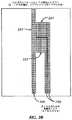
図2Bは、ピクセルにより使用されるLCD技術の形式に基づいて必要とされるか又は必要とされないCFガラスパターン化ITO領域レイアウトを示す。例えば、このようなCF ITO領域は、LCDピクセルがインプレーンスイッチング(IPS)を利用する場合には必要がない。しかしながら、図2Bは、上部電極と下部電極との間で液晶に電圧が印加される非IPS LCDディスプレイに向けられている。図2Bは、図2Aの下部(非IPSディスプレイにおける)領域201、205及び207に各々対応する上部領域221、223及び225を示している。図2Bは、領域251、255及び257に接触する導電性ドット250を示している。これら導電性ドット250は、対応する上部領域及び下部領域を接続して、上部領域におけるピクセルの上部電極が駆動されたとき、下部領域におけるピクセルの対応する下部電極も駆動されるようにする。その結果、ピクセルが、例えば、変調信号により駆動される間にも、上部電極と下部電極との間の相対的電圧は、一定に保たれる。従って、液晶に印加される電圧は、例えば、タッチ段階中に、一定に保持することができる。特に、一定の相対的電圧は、LCDピクセルを動作するためのピクセル電圧である。それ故、タッチ入力が検出される間に、ピクセルは、動作を続ける(即ち、映像を表示する)ことができる。 FIG. 2B shows a CF glass patterned ITO region layout that may or may not be required based on the type of LCD technology used by the pixel. For example, such CF ITO regions are not necessary if the LCD pixel utilizes in-plane switching (IPS). However, FIG. 2B is directed to a non-IPS LCD display where a voltage is applied to the liquid crystal between the upper and lower electrodes. FIG. 2B shows upper regions 221, 223, and 225 corresponding respectively to the lower (in non-IPS display)
図3ないし5Bを参照して、本発明の実施形態によるタッチ感知オペレーションを説明する。明瞭化のために、単一ドライブピクセル及び単一センスピクセルに関してオペレーションを説明する。しかしながら、上述したように、ドライブピクセルは、ドライブ領域の他のドライブピクセルに接続され、そしてセンスピクセルは、センス領域の他のセンスピクセルに接続されることが理解される。従って、実際のオペレーションでは、全ドライブ領域が駆動され、そして全センス領域がタッチの感知に貢献する。 With reference to FIGS. 3 to 5B, a touch sensing operation according to an embodiment of the present invention will be described. For clarity, operation will be described with respect to a single drive pixel and a single sense pixel. However, as described above, it is understood that the drive pixel is connected to other drive pixels in the drive region, and the sense pixel is connected to other sense pixels in the sense region. Thus, in actual operation, the entire drive area is driven and the entire sense area contributes to touch sensing.
図3は、ドライブ領域のピクセル301及び規範的センス領域のピクセル303の部分回路図を示す。ピクセル301及び303は、TFT307及び309、ゲートライン311及び312、データライン313及び314、xVcomライン315及び316、フリンジ電界電極319及び321、蓄積キャパシタ323及び325を含む。蓄積キャパシタ323及び325は、各々、約300fF(フェムトファラッド)のキャパシタンスを有する。ピクセル303のフリンジ電界電極321の下部電極は、xVcom316を経て、センス回路の電荷増幅器326に接続することができる。電荷増幅器326は、このラインをバーチャル接地に保持し、フリンジ電界電極321から注入される電荷が増幅器の電圧出力として現れるようにする。増幅器のフィードバック素子がキャパシタとして示されているが、抵抗器として働くこともできるし、又は抵抗器及びキャパシタの組み合わせとして働くこともできる。又、フィードバックは、例えば、タッチ感知回路のダイサイズを最小にするために抵抗器及びキャパシタフィードバックでもよい。図3は、カバーガラス(図示せず)とで約3fFの漂遊キャパシタンスを生じる指327、及び各約3fFであるピクセルの他の漂遊キャパシタンスも示している。 FIG. 3 shows a partial circuit diagram of a
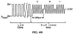
図4Aは、LCD段階中及びタッチ段階中にピクセル301を含むドライブ領域のピクセルへxVcom315を通して印加される規範的な信号を示す。LCD段階中に、xVcom315は、LCD反転を遂行するために2.5V±2.5Vの方形波信号で駆動される。LCD段階は、巾が12msである。タッチ段階では、xVcom315は、各々200マイクロ秒持続する15ないし20の連続する刺激段階で駆動される。この場合の刺激信号は、同じ周波数と、0°又は180°の相対的位相(図4Aにおいて“+”及び“−”に対応する)とを各々有する2.5V±2Vの正弦波信号である。タッチ段階は、巾が4msである。 FIG. 4A shows an exemplary signal applied through xVcom 315 to the pixels in the drive area that includes
図5Aは、タッチ段階中の蓄積キャパシタ323の動作を詳細に示す。より詳細には、蓄積キャパシタ323のキャパシタンスは、他のキャパシタンス、即ち図3に示す漂遊キャパシタンスより著しく高いので、蓄積キャパシタの下部電極に印加される2.5V±2Vの正弦波刺激信号のAC成分のほとんど(約90%)は、上部電極へ移送される。それ故、LCDを動作するために4.5ボルトDCまで荷電される上部電極は、4.5V±1.9Vの正弦波信号を見る。これらの信号は、フリンジ電界電極319の対応する左右の櫛形構造体へ通される。このように、フリンジ電界電極319の両櫛形構造体は、振幅が約±2V(一方は±2V、他方は±1.9V)のAC成分を有する信号で変調することができる。従って、フリンジ電界電極319は、同様に駆動されるドライブ領域におけるピクセルの他のフリンジ電界電極と共に、容量性感知のドライブ線として動作することができる。 FIG. 5A details the operation of the
フリンジ電界電極319は、タッチ感知システムのドライブ素子として動作するように構成されると同時に、LCDディスプレイシステムの一部分として動作を続けることに注意するのが重要である。図5Aに示すように、フリンジ電界電極の櫛形構造体の電圧は、各々、約±2Vで変調されるが、櫛形構造体間の相対的電圧は、2V±0.1Vでほぼ一定に留まる。この相対的電圧は、LCD動作のためにピクセルの液晶が見る電圧である。タッチ段階中の相対的電圧の0.1VAC変動がLCDディスプレイに及ぼす影響は、受け容れられる程度の低いものでなければならない。というのは、特に、AC変動は、典型的に、その周波数が液晶の応答時間より高いからである。例えば、刺激信号の周波数、ひいては、AC変動の周波数は、典型的に、100kHzより高い。しかしながら、液晶の応答時間は、典型的に、100Hz未満である。それ故、タッチシステムのドライブ素子としてのフリンジ電界電極の機能は、フリンジ電界電極のLCDの機能を妨げてはならない。 It is important to note that the
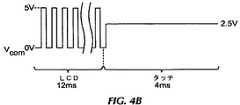
図3、4B及び5Bを参照し、センス領域の規範的動作について以下に述べる。図4Bは、上述したLCD及びタッチ段階中にピクセル303を含むセンス領域のピクセルへxVcom316を通して印加される信号を示す。ドライブ領域と同様に、xVcom316は、LCD段階中に、LCD反転を遂行するために2.5V±2.5Vの方形波信号で駆動される。タッチ段階中に、xVcom316は、2.5Vのバーチャル接地又はその付近に電圧を保持する増幅器326に接続される。従って、フリンジ電界電極321も、2.5Vに保持される。図3に示すように、フリンジ電界は、フリンジ電界電極319からフリンジ電界電極321へ伝播する。上述したように、フリンジ電界は、ドライブ領域により約±2Vで変調される。これらの電界がフリンジ電界電極321の上部電極により受け取られると、ほとんどの信号は、下部電極へ転送される。というのは、ピクセル303が、ピクセル301と同じ又は同様の漂遊キャパシタンス及び蓄積キャパシタを有するからである。xVcom316は、電荷増幅器326に接続され、そしてバーチャル接地に保持されるので、注入される電荷は、電荷増幅器の出力電圧として現れる。この出力電圧は、タッチ感知システムのためのタッチ感知情報を与える。例えば、指327は、フリンジ電界に接近すると、若干の電界を捕獲してそれを接地し、電界に擾乱を生じさせる。この擾乱は、電荷増幅器326の出力電圧の擾乱としてタッチシステムにより検出することができる。図5Bは、TFT325のドレインにも接続されたキャパシタの電極半部分に当たるピクセル302の受け取られたフリンジ電界のほぼ90%が電荷増幅器326へ転送されることを示している。XVCOM316に直結されたキャパシタの電極半部分に当たる電荷の100%が電荷増幅器326へ転送される。各電極に当たる電荷の比は、LCD設計に依存する。非IPSの場合、指により影響される電荷のほぼ100%が、VCOM電極に当たる。というのは、パターン化されたCFプレートが指の最も近くにあるからである。IPS型のディスプレイの場合、その比は、半分・半分に近づく。というのは、電極の各部分のほぼ同じ面積(又は1/4・対・3/4)が指に面するからである。あるサブ形式のIPSディスプレイの場合、フリンジ電極は、同一平面ではなく、上を向いた面積の大部分がVCOM電極にささげられる。 With reference to FIGS. 3, 4B and 5B, the normative operation of the sense region is described below. FIG. 4B shows the signals applied through xVcom 316 to the pixels in the sense
図3、4A−B及び5A−Bの規範的なドライブ及びセンス動作は、明瞭化のために、単一のピクセルを使用して説明する。本発明の実施形態によるドライブ領域及びセンス領域の規範的なレイアウト及び動作を、図6A−C、7、8A−C、9A−C、及び10を参照して以下に述べる。 The example drive and sense operations of FIGS. 3, 4A-B and 5A-B are described using a single pixel for clarity. An exemplary layout and operation of the drive and sense regions according to embodiments of the present invention is described below with reference to FIGS. 6A-C, 7, 8A-C, 9A-C, and 10. FIG.
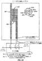
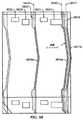
図6Aは、本発明の実施形態によりLCD素子として及びタッチセンサとして動作する二重機能容量性素子を伴うピクセルの領域を有する規範的タッチスクリーン600の部分図である。図6Aの例において、8列(aからhで示す)及び6行(1から6で示す)を有するタッチスクリーン600が示されているが、いかなる数の列及び行も使用できることを理解されたい。列aからhは、列状の領域から形成されるが、図6Aの例では、各列の片側が、各列に個別区分を生成するように設計された食い違った縁及びノッチを含む。行1ないし6の各々は、領域内の複数の個別のパッチ又はパッドから形成でき、各パッチは、タッチスクリーン600の境界エリアまで延びる1つ以上のyVcomラインを通して境界エリアへ接続され、特定の行の全てのパッチを、境界エリアに延びる金属トレース(図6Aには示さず)を通して一緒に接続できるようにしている。これらの金属トレースは、タッチスクリーン600の片側の小さなエリアへとルーティングされて、フレックス回路602に接続される。図6Aの例に示したように、行を形成するパッチは、例えば、一般的なピラミッド状構成で、xVcomライン及びyVcomラインに切断部を選択的に配置することにより形成できる。図6Aにおいて、例えば、列aとbとの間の行1から3のパッチは、逆ピラミッド構成で配置され、一方、列aとbとの間の行4から6のパッチは、直立ピラミッド構成で配置される。 FIG. 6A is a partial view of an
図6Bは、本発明の実施形態によりタッチスクリーンの境界領域に延びる金属トレース604及び606を含む規範的タッチスクリーン600の部分図である。図6Bの境界エリアは、明瞭化のために拡大されていることに注意されたい。各列a−hは、ビア(図6Bには示さず)を通して列を金属トレースに接続できるようにする拡張yVcomライン608を含む。各列の片側は、各列に個別の区分を生成するように設計された食い違った縁614及びノッチ616を含む。各行パッチ1−6は、ビア(図6Bには示さず)を通してパッチを金属トレースに接続できるようにする拡張yVcomライン610を含む。yVcomライン610は、特定の行の各パッチを互いに自己接続できるようにする。全ての金属トレース604及び606は、同じ層上に形成されるので、全てを同じフレックス回路602へルーティングすることができる。 FIG. 6B is a partial view of an
タッチスクリーン600が相互キャパシタンスタッチスクリーンとして動作される場合には、列a−h又は行1−6のいずれかを、1つ以上の刺激信号で駆動することができると共に、隣接列エリアと行パッチとの間にフリンジ電界線を形成することができる。図6Bにおいて、列aと行パッチ1との間(a−1)の電界線612のみが説明上示されているが、どんな列又は行が刺激されるかに基づいて他の隣接列と行パッチとの間(例えば、a−2、b−4、g−5、等)にも電界線を形成できることを理解されたい。従って、各列−行パッチ対(例えば、a−1、a−2、b−4、g−5、等)は、ドライブ領域からセンス領域へ電荷を結合できるところの2領域タッチピクセル又はセンサを表すことを理解されたい。これらタッチピクセルの1つに指がタッチダウンすると、タッチスクリーンのカバーを越えて延びるフリンジ電界線の幾つかが指によって阻止されて、センス領域に結合される電荷の量を減少させる。結合される電荷の量のこの減少は、それにより生じるタッチの「映像」を決定する部分として検出することができる。図6Bに示す相互キャパシタンスタッチスクリーン設計では、個別の基準接地が必要とされず、従って、基板の背面上又は個別基板上に第2層を設ける必要がないことに注意されたい。 If
又、タッチスクリーン600は、自己キャパシタンスタッチスクリーンとして動作することもできる。このような実施形態では、基板の背面、パッチ及び列と同じ側であるが、パッチ及び列から誘電体により分離されて、又は個別の基板上に、基準接地平面を形成することができる。自己キャパシタンスタッチスクリーンでは、各タッチピクセル又はセンサは、基準接地に対する自己キャパシタンスを有し、これは、指の存在により変化する。自己キャパシタンスの実施形態では、列a−hの自己キャパシタンスを独立して感知することができ、そして行1−6の自己キャパシタンスも独立して感知することができる。 The
図6Cは、本発明の実施形態によるタッチスクリーンの境界領域における金属トレースへの列及び行パッチの規範的な接続を示す。図6Cは、図6Bに示す「詳細A」を表すと共に、yVcomライン608及び610を通して金属トレース618に接続された列「a」及び行パッチ4−6を示す。yVcomライン608及び610は、誘電体材料により金属トレース618から分離されているので、誘電体材料に形成されるビア620は、yVcomラインを金属トレースに接続できるようにする。金属トレース618は、yVcomラインと同じ層に形成することができる。この場合、付加的なプロセスステップはなく、タッチトレースは、LCDに従来からある「ゲート金属」及び「ソース/ドレイン金属」とも称される同じM1及びM2層においてルーティングすることができる。又、誘電体絶縁層は、「内部層誘電体」又は「ILD」とも称される。 FIG. 6C illustrates an exemplary connection of column and row patches to metal traces in the border area of the touch screen according to an embodiment of the present invention. FIG. 6C represents “detail A” shown in FIG. 6B and shows column “a” and row patches 4-6 connected to
図6Cに示すように、列の縁614及び行パッチ4−6は、x方向に食い違っている。というのは、行パッチ4及び5を接続するyVcomライン610を収容するスペースをタッチピクセルに対して作らねばならないからである。(図6Cの例における行パッチ4は、実際には、2つのパッチが一緒に接着されたものであることを理解されたい。)最適なタッチ感度を得るため、タッチピクセルa−6、a−5及びa−4において領域の面積のバランスをとることが望まれる。しかしながら、列「a」が直線に保たれる場合には、行パッチ6は、行パッチ5又は6より細くすることができ、タッチピクセルの領域a−6間でアンバランスが生じることになる。 As shown in FIG. 6C, the column edges 614 and the row patches 4-6 are misaligned in the x direction. This is because a space for accommodating the
図7は、本発明の実施形態による規範的な列及び隣接行パッチの上面図である。一般的に、タッチピクセルa−4、a−5及びa−6の相互キャパシタンス特性を比較的一定にして、タッチ感知回路の範囲内に留まる比較的均一のz方向タッチ感度を生じさせることが望まれる。従って、列エリアa4、a5及びa6は、行パッチエリア4、5及び6とほぼ同じでなければならない。これを達成するために、列区分a4及びa5、並びに行パッチ4及び5は、列区分a6及び行パッチ6に比してy方向に収縮して、列セグメントa4の面積を列セグメントa5及びa6の面積に一致させることができる。換言すれば、タッチピクセルa4−4は、狭いが高いタッチピクセルa6−6より広いが短い。FIG. 7 is a top view of an exemplary column and adjacent row patch according to an embodiment of the present invention. In general, it is desirable to make the mutual capacitance characteristics of touch pixels a-4, a-5 and a-6 relatively constant, resulting in a relatively uniform z-direction touch sensitivity that remains within the touch sensing circuitry. It is. Thus, the column areas a4 , a5 and a6 must be substantially the same as the
タッチピクセル又はセンサは、x方向に若干スキューされ又は不整列であるので、タッチピクセルa−6における最大タッチ事象(タッチピクセルa−6の真上に下された指)のx座標は、例えば、タッチピクセルa−4における最大タッチ事象のx座標とは若干異なる。従って、本発明の実施形態では、この不整列は、タッチピクセルを再マップして歪みを除去するようにソフトウェアアルゴリズムで脱ワープ(de-warp)することができる。 Since the touch pixel or sensor is slightly skewed or misaligned in the x direction, the x coordinate of the maximum touch event at finger pixel a-6 (finger that has been dropped directly above touch pixel a-6) is, for example: The x coordinate of the maximum touch event in touch pixel a-4 is slightly different. Thus, in embodiments of the present invention, this misalignment can be de-warped with a software algorithm to remap the touch pixels to remove the distortion.
典型的なタッチパネルグリッド寸法は、タッチパネルを中心間5.0mmで配置することができるが、タッチスクリーンにおいて電気的接続の全体数を減少するには、例えば、中心間約6.0mmのより広げられたグリッドが望まれる。しかしながら、センサパターンを広げると、誤ったタッチの読みを生じることがある。 Typical touch panel grid dimensions allow the touch panel to be placed 5.0 mm center-to-center, but to reduce the overall number of electrical connections in the touch screen, for example, more than about 6.0 mm center-to-center. A grid is desired. However, widening the sensor pattern may result in erroneous touch readings.
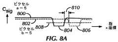
図8Aは、単一の行において広い間隔をもつ2つの隣接するタッチピクセルa−5及びb−5に対して、指タッチのx座標・対・タッチピクセルから見た相互キャパシタンスを示す規範的グラフである。図8Aにおいて、曲線800は、指タッチが左から右へ連続的に移動するときにタッチピクセルa−5から見た相互キャパシタンスを表し、曲線802は、指タッチが左から右へ連続的に移動するときにタッチピクセルb−5から見た相互キャパシタンスを表す。予想されるように、相互キャパシタンス804の降下は、指タッチがタッチピクセルa−5の真上を通過するときにタッチピクセルa−5において見られ、そして相互キャパシタンス806の同様の降下は、指タッチがタッチピクセルb−5の真上を通過するときにタッチピクセルb−5において見られる。線808が、タッチ事象を検出するためのスレッシュホールドを表す場合には、図8Aは、指がタッチスクリーンの表面から持ち上げられなくても、810において、誤って、指が表面から瞬間的に持ち上がったように見えることを示している。この位置810は、2つの広がったタッチピクセル間のほぼ中間点を表す。 FIG. 8A is a canonical graph showing the mutual capacitance seen from the x coordinate of a finger touch versus the touch pixel for two adjacent touch pixels a-5 and b-5 that are widely spaced in a single row. It is. In FIG. 8A,
図8Bは、本発明の実施形態により空間的補間が行われる場合に単一の行において広い間隔をもつ2つの隣接するタッチピクセルa−5及びb−5に対し、指タッチのx座標・対・タッチピクセルから見た相互キャパシタンスを示す規範的グラフである。予想されるように、相互キャパシタンス804の降下は、指タッチがタッチピクセルa−5の真上を通過するときにタッチピクセルa−5において見られ、そして相互キャパシタンス806の同様の降下は、指タッチがタッチピクセルb−5の真上を通過するときにタッチピクセルb−5において見られる。しかしながら、相互キャパシタンス値の上昇及び降下は、図8Aの場合より緩やかに生じることに注意されたい。線808が、タッチ事象を検出するためのスレッシュホールドを表す場合には、図8Bは、指がタッチピクセルa−5及びb−5の上を左から右へ移動するときに、タッチ事象は、常に、タッチピクセルa−5又はb−5のいずれかにおいて検出されることを示している。換言すれば、タッチ事象のこの「ボケ」は、偽のノータッチ読みが現れるのを防止するのに有用である。 FIG. 8B illustrates a finger touch x-coordinate pair for two adjacent touch pixels a-5 and b-5 that are widely spaced in a single row when spatial interpolation is performed according to an embodiment of the present invention. A normative graph showing the mutual capacitance as seen from the touch pixel. As expected, a drop in
本発明の一実施形態では、図8Bに示す空間的なボケ又はフィルタリングの一部分又は全部を生成するために、タッチスクリーンのためのカバーガラスの厚みを増加することができる。 In one embodiment of the present invention, the thickness of the cover glass for the touch screen can be increased to produce part or all of the spatial blur or filtering shown in FIG. 8B.
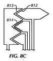
図8Cは、本発明の実施形態により大きなタッチピクセル間隔に対して有用な規範的な列及び隣接行パッチパターンの上面図である。図8Cは、x方向に延びるタッチピクセル内に鋸歯状領域縁812が使用される規範的実施形態を示す。鋸歯状領域縁は、フリンジ電界線814が大きなエリア上にx方向に存在できるようにし、x方向に大きな距離にわたり同じタッチピクセルによりタッチ事象を検出できるようにする。図8Cの鋸歯状構成は、一例に過ぎず、曲がりくねった縁、等の他の構成も使用できる。これらの構成は、更に、タッチパターンを軟化し、そして図8Bに示すように、隣接するタッチピクセル間に付加的な空間的フィルタリング及び補間を生成することができる。 FIG. 8C is a top view of an exemplary column and adjacent row patch pattern useful for large touch pixel spacings according to embodiments of the present invention. FIG. 8C shows an exemplary embodiment in which serrated region edges 812 are used in touch pixels extending in the x-direction. The serrated region edge allows
図9Aは、本発明の実施形態により、多角形領域(レンガ)902の列906及び行として形成されたセンス(又はドライブ)領域(C0−C5)を含む規範的タッチスクリーン900であって、レンガの各行が個別のドライブ(又はセンス)領域(R0−R7)を形成するものを示す。図9Aの例では、接続yVcomライン904は、レンガの片側のみに沿ってルーティングされる(いわゆる「単一脱出」構成)。6列及び8行のタッチスクリーン900が示されているが、いかなる数の列及び行も使用できることを理解されたい。 FIG. 9A illustrates an
特定行におけるレンガ902を一緒に結合するため、接続yVcomライン904を、レンガから、単一脱出構成のレンガの片側に沿って、特定のバスライン910へルーティングすることができる。接地分離領域908を接続yVcomライン904と隣接列906との間に形成して、接続yVcomラインと列との間の容量性結合を減少することができる。各バスライン910及び列906に対する接続は、タッチスクリーン900からフレックス回路912を経て行うことができる。 In order to join the
図9Bは、図9Aの規範的タッチスクリーン900の一部分の拡大図で、本発明の実施形態により単一脱出構成において接続yVcomライン904を使用してレンガ902をバスライン910へどのようにルーティングできるかを示す。図9Bにおいて、トレースの全抵抗率を等化すると共に、ドライブ回路から見た全容量性負荷を最小にするために、短い接続yVcomライン(例えば、トレースR2)よりも長い接続、即ちyVcomライン904(例えば、トレースR7)を使用することができる。 FIG. 9B is an enlarged view of a portion of the
図9Cは、本発明の実施形態により列C0及びC1に関連したレンガ902及びこれらレンガをバスライン910に結合する接続yVcomライン904(細い線として記号的に示す)を含む図9Aの規範的タッチスクリーン900の一部分を示す図である。記号的に描かれそして例示のために一定の縮尺率で描かれていない図9Bの例では、バスラインB0がレンガR0C0(列C0に隣接しB0に最も近いレンガ)及びR0C1(列C1に隣接しB0に最も近いレンガ)に結合されている。バスラインB1は、レンガR1C0(列C0に隣接しB0に次に最も近いレンガ)及びR1C1(列C1に隣接しB0に次に最も近いレンガ)に結合される。このパターンが他のバスラインに対して繰り返され、バスラインB7は、レンガR7C0(列C0に隣接しB0から最も遠いレンガ)及びR7C1(列C1に隣接しB0から最も遠いレンガ)に結合される。 FIG. 9C illustrates the example touch of FIG.
図10は、本発明の実施形態により接続yVcomラインとセンス領域との間の漂遊キャパシタンスを更に減少できる規範的ジグザグ二重補間タッチスクリーン1000の一部分を示す図である。図10の例では、ドライブ(又はセンス)領域を表す多角形領域1002は、一般的に、五角形の形状で且つ方向が食い違わされ、パネルの端部付近の多角形エリアの幾つかは、切断された五角形である。センス(又はドライブ)領域1004は、ジグザグ形状で、センス(又はドライブ)領域と五角形1002との間に接地ガード1006が設けられている。全ての接続yVcomライン1008は、五角形1002間のチャンネル1010内にルーティングされる。相互キャパシタンスの実施形態では、各タッチピクセル又はセンサは、五角形と隣接センス(又はドライブ)領域1004との間に形成される電界線1016により特徴付けられる。接続yVcomライン1008は、センス(又はドライブ)領域1004に沿って延びず、五角形1002間に延びるので、接続yVcomライン1008とセンス(又はドライブ)領域1004との間の漂遊キャパシタンスが最小にされると共に、空間的交差結合も最小にされる。以前は、接続yVcomライン1008とセンス(又はドライブ)領域1004との間の距離は、接地ガード1006の巾だけであったが、図10の実施形態では、この距離が、接地ガードの巾と五角形1002の巾(その形状の長さに沿って変化する)との和となる。 FIG. 10 is a diagram illustrating a portion of an exemplary zigzag double interpolated
図10の例に示されるように、タッチスクリーンの端における行R14の五角形は裁断することができる。従って、R14に対するタッチ1012の計算された重心は、その真の位置からy方向にオフセットすることができる。加えて、2つの隣接行に対するタッチの計算された重心は、オフセット距離だけx方向に食い違わされる(互いにオフセットされる)。しかしながら、この不整列は、タッチピクセルを再マップすると共に歪みを除去するために、ソフトウェアアルゴリズムで脱ワープすることができる。 As shown in the example of FIG. 10, the pentagon in row R14 at the edge of the touch screen can be cut. Thus, the calculated center of gravity of
本発明の以上の実施形態は、主として、ここでは、相互キャパシタンスタッチスクリーンに関して説明したが、本発明の実施形態は、自己キャパシタンスタッチスクリーンにも適用できることを理解されたい。このような実施形態では、基板の背面に、又は多角形領域及びセンス領域と同じ基板の側であるが多角形領域及びセンス領域から誘電体によって分離されて、或いは個別の基板上に、基準接地平面を形成することができる。自己キャパシタンスタッチスクリーンでは、各タッチピクセル又はセンサは、指の存在により変更できる基準接地に対する自己キャパシタンスを有する。タッチスクリーンは、相互及び自己キャパシタンスの両方の測定を時間マルチプレクス形態で使用して、付加的な情報を収集できると共に、各測定形式で互いに弱点を補償することができる。 Although the above embodiments of the present invention have been described primarily herein with respect to mutual capacitance touch screens, it should be understood that embodiments of the present invention are also applicable to self-capacitance touch screens. In such an embodiment, a reference ground is provided on the back of the substrate or on the same substrate side as the polygonal region and sense region, but separated from the polygonal region and sense region by a dielectric, or on a separate substrate. A plane can be formed. In a self-capacitance touch screen, each touch pixel or sensor has a self-capacitance with respect to a reference ground that can be changed by the presence of a finger. The touch screen can use both mutual and self-capacitance measurements in a time multiplexed fashion to collect additional information and compensate for each other's weaknesses in each measurement format.
本発明の実施形態により、二重機能の容量性素子を伴うピクセルを含む規範的ディスプレイと、このディスプレイを製造するプロセスとについて、図11ないし46を参照して以下に説明する。図11ないし24は、アモルファスシリコン(a−Si)を使用する規範的な電気的制御型複屈折(ECB)LCDディスプレイに向けられる。図23ないし34は、低温多結晶シリコン(LTPS)を使用する規範的IPS LCDディスプレイに向けられる。図35ないし43は、LTPSを使用する別の規範的なIPS LCDディスプレイに向けられる。図44ないし55は、LTPSを使用する規範的なECB LCDディスプレイに向けられる。 An exemplary display including pixels with dual-function capacitive elements and a process for manufacturing the display according to embodiments of the present invention is described below with reference to FIGS. FIGS. 11-24 are directed to an exemplary electrically controlled birefringence (ECB) LCD display using amorphous silicon (a-Si). FIGS. 23-34 are directed to an exemplary IPS LCD display using low temperature polycrystalline silicon (LTPS). FIGS. 35-43 are directed to another exemplary IPS LCD display using LTPS. Figures 44 through 55 are directed to an example ECB LCD display using LTPS.
本発明の実施形態によりECB LCDディスプレイを製造する規範的プロセスを、図11ないし18を参照して以下に説明する。これらの図は、ECB LCDディスプレイの製造中に2つのピクセル、即ちピクセル1101及びピクセル1102を処理する種々の段階を示している。それにより生じるピクセル1101及び1102は、各々、図1のピクセル101及び102と等価な電気回路を形成する。 An exemplary process for manufacturing an ECB LCD display according to an embodiment of the present invention is described below with reference to FIGS. These figures illustrate the various stages of processing two pixels, namely
図11は、ピクセル1101及び1102の第1の金属層(M1)のパターンを示す。図11に示すように、ピクセル1102のM1層は、ゲート1155aと、ゲートライン1113の一部分1113bと、蓄積キャパシタの下部電極1157b(下部電極1157b以外は図示せず)と、xVcom1121の一部分1121bとを含む。ピクセル1101は、ゲート1105aと、蓄積キャパシタの下部電極1107b(下部電極1107b以外は図示せず)と、ゲートライン1113の一部分1113aと、xVcom1121の一部分1121aとを含む。又、ピクセル1101は、yVcom1123(点線で示す)の一部分1123aを含み、これは、付加的な部分1140を含む。部分1123aは、接続点1141及び接続点1143を有する。図11に示すように、ゲートライン1113及びxVcom1121は、両ピクセル1101及び1102を通してx方向に延びる。ゲートライン1113は、ゲート1105a及び1155aに接続され、そしてxVcom1121は、下部電極1107b及び1157bに接続される。yVcom1123の一部分1123aは、ピクセル1101のxVcom1121に接続される。 FIG. 11 shows the pattern of the first metal layer (M1) of the
図12は、ポリSiのアイランドパターンが形成される、ピクセル1101及び1102の製造プロセスにおけるその後のパターン化ステップを示す。図12において明らかなように、ピクセルに対するアイランドパターンは同様であるが、ピクセル1102の半導体部分1201及び1203は、ピクセル1101の半導体部分1205及び1207とは若干異なる。例えば、部分1205は、部分1201より若干小さい。これは、一部分は、以下に詳細に述べるように、xVcom1121を、yVcom1123を通して他のxVcomラインと垂直方向(y方向)に接続できるようにするためである。 FIG. 12 shows the subsequent patterning steps in the manufacturing process of
図13は、ピクセル1101に形成された接続部1301及び1302を示す。ピクセル1102は、このような接続を含まない。接続1301及び1302の動作は、図14を参照して以下に詳細に述べる。 FIG. 13
図14は、ピクセル1101及び1102の第2の金属層(M2)のパターン化を示す。図14に示したように、ピクセル1102のM2層は、グリーンカラーデータラインGdata1417(図14では点線で示す)の一部分1417aと、ソース1455bと、ドレイン1455cと、上部電極1457aとを形成する。ピクセル1102と同様に、ピクセル1101のM2層は、レッドカラーデータラインRdata1415(図14では点線で示す)の一部分1415aと、ソース1405bと、ドレイン1405cと、上部電極1407aとを形成する。又、ピクセル1101のM2層は、yVcom1123(図14では点線で示す)の一部分1423a及び1423bを形成する。上部電極1407aは、上部電極1457aと同様であり、これは、ピクセル1101のM2レイヤに部分1423aを形成できるようにする。部分1423aは、接続点1441を有し、そして部分1423bは、接続点1443を有する。 FIG. 14 shows the patterning of the second metal layer (M2) of the
図11、13及び14は、xVcom1121を垂直方向(y方向)に他のxVcomラインと接続できるようにする垂直の共通ライン(yVcom1415)をピクセル1101が含むことを示している。特に、これらの図は、部分1423aが接続部1301を通して各々接続点1441及び1141において部分1123aに接続されることを示している。部分1123aは、接続部1302を通して各々点1143及び1443において1423bに接続される。従って、これらの図は、yVcom1123の連続部分が、ピクセル1101において、ピクセルの複数構造体の接続により形成されることを示している。又、図11に示すように、yVcom1123aは、xVcom部分1121aに接続される。従って、これらの図に示されたピクセル1101の構造体は、複数のxVcomラインを垂直方向に接続できるようにする。 11, 13 and 14 show that the
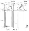
図15は、ピクセル1101及び1102の平坦化(PLN)接触層各々1501及び1503を示す。図16は、ピクセル1101及び1102の反射(REF)層各々1601及び1603を示す。図17は、ピクセル1101及び1102の不動態(PASS)接触部各々1701及び1703を示す。図18は、ピクセル1101及び1102のピクセル電極各々1801及び1803を形成するIPO層のような半透明導電性材料層を示す。 FIG. 15 shows the planarization (PLN)
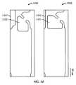
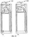
図19は、完成したピクセル1101及び1102の平面図である。図20A−Bは、これらの図の上面図に示す経路に沿ってとられた完成したピクセル1101の側面図である。図20C−D図は、図19に示す線に沿ったピクセル1101及び1102の側面図である。 FIG. 19 is a plan view of completed
図20Aは、ピクセル1101の側面図である。図20Aに示すM1層の一部分は、ゲートライン部分1113bと、ゲート1155aと、下部電極1157bと、xVcom部分1121bとを含む。図20Aに示すポリSi層は、ポリSi1205及びポリSi1201を含む。図20Aに示すM2層は、ソース1455bと、ドレイン1465cと、上部電極1457aとを含む。又、図20Aは、平坦化層1503、反射層1603、不動態化接触部1703、及び透明導体層1103も示す。 FIG. 20A is a side view of the
図20Bは、ピクセル1101の別の側面図である。明瞭化のために、平坦化接触部、反射部、不動態化接触部、及び透明導体層は、図示されていない。図20Bに示すM1層は、ゲートライン部分1113aと、ゲート1105aと、下部電極1107bと、xVcom部分1121aとを含む。又、図20Bは、ピクセル1101と同じ構造を有する隣接ピクセル2001も示す。図20Bに示されたポリSi層は、ポリSi部分1211及びポリSi部分1207を含む。図20Bに示されたM2層は、ソース1405b、ドレイン1405c及び上部電極1407aを含む。 FIG. 20B is another side view of the
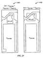
図20Cは、図19に示す線に沿ったピクセル1102の側面図である。図20Cに示されたM1層は、ゲートライン部分1113bと、ゲート1155aと、xVcom部分1121bとを含む。又、図20Cは、M1の頂部に堆積されたゲート絶縁体2003も示す。又、図20Cには、ポリSi部分1203及び付加的なポリSi部分も示されている。 20C is a side view of
図20Dは、図19に示す線に沿ったピクセル1101の側面図である。図20Dに示すM1層は、ゲートライン部分1113aと、ゲート1105aと、yVcom部分1123aとを含み、これは、xVcom部分1121aとの交点を含む。接続部1301及び1302は、yVcom部分1123aの接続点1141及び1143に各々接触する。又、図20Dは、ゲート絶縁体層2005及びポリSi部分1209も示している。図20Dに示すM2層は、接続点1441において接続部1301に接続されるyVcom部分1423aと、接続点1443において接続部1302に接続されるyVcom部分1423bとを含む。垂直の共通ラインyVcom1123(図20Dでは点線として示す)は、yVcom部分1423a、接続部1301、yVcom部分1123a、接続部1302、及びyVcom部分1423bとしてピクセル1181を通して延びる。又、図20Dは、ピクセル1101と同一の構造を含む隣接ピクセルの一部分も示している。特に、隣接ピクセルは、接続部を経てxVcom部分に接続されたyVcom部分を含む。従って、図20Dは、xVcom部分1121aをyVcomラインでその隣接ピクセルのxVcom部分へ接続できることを示す。 20D is a side view of the
図21及び22は、ピクセル1101及び1102の蓄積キャパシタンスの比較分析を示す。ピクセル1102の全蓄積キャパシタンス(Cstore)は、次の通りである。
Cstore=CM1/M2+CM1/ITO (1)
但し、CM1/M2は、ピクセル1102の上部電極1457a及び下部電極1157bのような重畳するM1及びM2層のキャパシタンスであり、
CM1/ITOは、第1金属層と透明な導体層との重畳するエリア間のキャパシタンスである。21 and 22 show a comparative analysis of the stored capacitance of
Cstore = CM1 / M2 + CM1 / ITO (1)
Where CM1 / M2 is the capacitance of the overlapping M1 and M2 layers such as the
CM1 / ITO is the capacitance between the overlapping areas of the first metal layer and the transparent conductor layer.
例えば、図21は、キャパシタンスCM1/M2を生じる第1及び第2の金属層の重畳するエリアを示す。図21に示すように、ピクセル1102のCM1/M2は、第1及び第2の金属層の約360平方マイクロメータの重畳から生じる。図22を参照すれば、ピクセル1102のハイライト部分は、CM1/ITOを生じる第1金属層及び透明導体層の重畳領域を示す。図22に示すように、全重畳は、約360平方マイクロメータである。For example, FIG. 21 shows the overlapping areas of the first and second metal layers that produce capacitance CM1 / M2 . As shown in FIG. 21, CM1 / M2 of
対照的に、ピクセル1101の全キャパシタンスは、次の通りである。
Cstore=CM1/M2+CM1/ITO+CM2/ITO (2)
但し、CM1/M2及びCM1/ITOは、前記で定義された通りであり、
CM2/ITOは、第2金属層と透明導体層との重畳から生じるキャパシタンスである。In contrast, the total capacitance of
Cstore = CM1 / M2 + CM1 / ITO + CM2 / ITO (2)
Where CM1 / M2 and CM1 / ITO are as defined above,
CM2 / ITO is a capacitance resulting from the superposition of the second metal layer and the transparent conductor layer.
ピクセル1101に対する蓄積キャパシタンス方程式の付加的な項CM2/ITOは、透明導体層と重畳するピクセル1101の第2の金属層の付加的なエリアから生じる。図21及び22は、ピクセル1101における重畳する金属のエリアから式2の項が生じることを示している。図21は、約503平方マイクロメータに等しいピクセル1101の第1及び第2の金属層の重畳領域を示している。図22は、約360平方マイクロメータに等しいピクセル1101の第1金属層及び透明導体層の重畳領域を示す。又、図22は、約81平方マイクロメータに等しい第2金属層及び透明導体層の重畳領域も示す。従って、図21及び22から、ピクセル1101の第1及び第2の金属層の重畳面積は、ピクセル1102の対応面積より小さいが、ピクセル1101は、ピクセル1102にはない特別の重畳面積を有する。特に、ピクセル1101における第2金属層と透明導体層との重畳は、付加的な81平方マイクロメータに貢献し、これは、ひいては、ピクセル1101の蓄積キャパシタンスに対する付加的なキャパシタンス量に貢献する。The additional term CM2 / ITO of the storage capacitance equation for
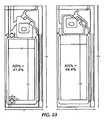
図23は、ピクセル1101及び1102のアパーチャー比の推定を示す。ピクセル1101は、41.4%のアパーチャー比を有する。ピクセル1102は、44.4%のアパーチャー比を有する。 FIG. 23 shows an estimation of the aperture ratio of
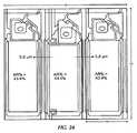
図24は、本発明の実施形態による規範的な変更を示す。この変更の結果として、システムにおける異なるピクセルのアパーチャー比がより類似したものとなり、表示の見掛けを改善する。ピクセル1102と同様、ピクセル2401及び2405は、y方向に接続部を含まない。他方、ピクセル2403は、ピクセル1101と同様、y方向に接続部を含む。 FIG. 24 illustrates example changes according to embodiments of the present invention. As a result of this change, the aperture ratio of different pixels in the system becomes more similar, improving the appearance of the display. Similar to
図25ないし34は、低温多結晶シリコン(LTPS)を使用する規範的IPS LCDディスプレイに向けられる。本発明の実施形態によりLTPSを使用するIPS LCDディスプレイを製造する規範的プロセスを、図25ないし31を参照して以下に説明する。これらの図は、LTPSを使用するIPS LCDディスプレイの製造中にピクセル2501及び2502の2つのピクセルを処理する種々の段階を示す。それにより得られるピクセル2501及び2502は、図1のピクセル各々101及び102と同等の電気回路を形成する。図25ないし30に示す処理段階は、ピクセル2501及びピクセル2502で同じであるから、これらの図の各々には1つのピクセルしか示さない。しかしながら、図25ないし30に示す処理段階は、ピクセル2501及びピクセル2502の両方に適用されることを理解されたい。 FIGS. 25-34 are directed to an exemplary IPS LCD display using low temperature polycrystalline silicon (LTPS). An exemplary process for manufacturing an IPS LCD display using LTPS according to embodiments of the present invention is described below with reference to FIGS. These figures illustrate the various stages of processing two pixels,
図25は、ピクセル2501及び2502のポリSiの層のパターン化を示している。半導体部分2505、2507及び2509は、TFTの活性領域を形成し、各々、ソース、ゲート及びドレインとして働く。 FIG. 25 shows the patterning of the poly-Si layer of
図26は、ピクセル2501及び2502を製造するプロセスにおいてピクセル2501及び2502の第1金属層(M1)が形成されるその後のパターン化ステップを示す。図26に示すように、ピクセル2501及び2502のM1層は、ゲート2605a、ゲートライン2613(点線で示す)の一部分2613a、及びxVcom2621の一部分2621aを含む。この部分2621aは、接続点2623を含む。ゲートライン2613及びxVcom2621は、x方向に隣接するピクセルを通して延びる。 FIG. 26 illustrates a subsequent patterning step in which the first metal layer (M1) of
図27は、部分2505、部分2509及び接続点2623に各々接続するためにピクセル2501及び2502に形成されたビア2701、2703及び2705を示す。 FIG. 27 shows vias 2701, 2703 and 2705 formed in
図28は、ピクセル2501及び2502の第2金属層(M2)のパターン化を示す。図28に示すように、ピクセルのM2層は、カラーデータライン2817(図28に点線で示す)の一部分2817aを形成し、これは、例えば、レッド、グリーン又はブルーのカラーデータを搬送する。部分2817aは、ビア2701を通して部分2505へ接続される接続部2819を含む。又、M2層は、ビア2703を通して部分2509との接続部2821を形成すると共に、ビア2705を通して接続点2623への接続部2823も形成する。 FIG. 28 shows the patterning of the second metal layer (M2) of
図29は、ピクセル2501及び2502に形成されたITOのような透明導電性材料の第1層を示している。この第1の透明導体層は、ピクセル電極2901を含む。又、図29は、x方向に隣接するピクセルのピクセル電極の一部分2905と、y方向に隣接するピクセルのピクセル電極の一部分2907も示している。又、図29は、接続点2623を通して以下に述べる共通のITO層とxVcom2621との間に接続部を形成する接続部2903と、図30に示す接続部3001も示している。 FIG. 29 shows a first layer of transparent conductive material, such as ITO, formed on the
図31は、ピクセル2501及び2502に形成されたITOのような透明導体の第2層を示す。ピクセル2502上の第2層は、共通電極3151を形成し、これは、接続部3001及び2903を通してxVcom2621に接続される接続点3153と、接続点2623とを含む。又、図31は、y方向に隣接するピクセルの共通電極の一部分3155も示している。ピクセル2502と同様に、ピクセル2501は、透明導体の第2層で形成された共通電極3101を含む。同様に、共通電極3101は、接続部3001及び2903を通してxVcom2621に接続される接続点3103と、接続点2623とを含む。しかしながら、ピクセル2501は、y方向に隣接するピクセルの共通電極3101と共通電極3105との間の接続部3107も含む。このように、ピクセルの共通電極は、y方向に接続されて、yVcomライン3109を形成する。共通電極3101がxVcom2621に接続され、そしてxVcom2621がx方向に他のピクセルの共通電極に接続されるので、ピクセルの領域の共通電極を一緒に接続して、タッチ感知素子を形成することができる。先の規範的実施形態と同様に、xVcomライン及びyVcomラインの切断部は、タッチセンサのアレイとして形成できる一緒にリンクされる共通電極の個別領域を生成することができる。 FIG. 31 shows a second layer of transparent conductor, such as ITO, formed on the
図32は、完成したピクセル2501及び2502の平面図である。図33は、図中に示された上面図に示す線に沿ってとられたピクセル2501の側面図である。 FIG. 32 is a plan view of completed
図34は、ピクセル2501及びピクセル2502の蓄積キャパシタンスを示す。 FIG. 34 shows the storage capacitance of
図35ないし43は、LTPSを使用する別の規範的IPS LCDディスプレイに向けられる。ここに示す例では、yVcomラインがM2層に形成される(yVcomラインが共通のITO層に形成された先の規範的IPS LCDディスプレイに比して)。本発明の実施形態によりM2層yVcomラインと共にLTPSを使用するIPS LCDディスプレイを製造する規範的プロセスを、図35ないし41を参照して以下に説明する。これらの図は、規範的IPS LCDディスプレイの製造中にピクセル3501及び3502の2つのピクセルを処理する種々の段階を示す。それにより生じるピクセル3501及び3502は、図1のピクセル101及び102と等価な電気回路を形成する。 FIGS. 35-43 are directed to another example IPS LCD display using LTPS. In the example shown here, a yVcom line is formed in the M2 layer (as compared to the previous example IPS LCD display where the yVcom line is formed in a common ITO layer). An exemplary process for manufacturing an IPS LCD display using LTPS with an M2 layer yVcom line according to embodiments of the present invention is described below with reference to FIGS. These figures show various stages of processing two pixels,
図35は、ピクセル3501及び3502のポリSiの層のパターン化を示す。半導体部分3505、3507及び3509は、ピクセル3501のTFTの活性領域を形成し、各々、ソース、ゲート及びドレインとして働く。同様に、半導体部分3506、3508及び3510は、各々、ピクセル3502のソース、ゲート及びドレインである。又、図35は、ピクセル3501の巾W’(x方向)がピクセル3502の巾Wより若干大きいことも示している。 FIG. 35 shows the patterning of the poly-Si layer of
図36は、ピクセル3501及び3502を製造するプロセスにおいてピクセル3501及び3502の第1金属層(M1)を形成するその後のパターン化ステップを示している。図36に示すように、ピクセル3501及び3502のM1層は、ゲート3605a及び3606aと、ゲートライン3613(点線で示す)の部分3613a及び3613bと、xVcom3621の部分3621a及び3621bとを含む。これら部分3621a及び3622aは、各々、接続点3623及び3624を含む。ゲートライン3613及びxVcom3621は、x方向に隣接するピクセルを通して延びる。 FIG. 36 illustrates the subsequent patterning step of forming the first metal layer (M1) of the
図37は、部分3505、部分3509及び接続点3623に接続するためにピクセル3501に各々形成されたビア3701、3703及び3705を示している。又、部分3506、部分3510及び接続点3624に接続するためにピクセル3502に各々形成されたビア3702、3704及び3706も示されている。 FIG. 37 shows vias 3701, 3703 and 3705 formed in the
図38は、ピクセル3501及び3502の第2金属層(M2)のパターン化を示す。ピクセル3501の場合に、M2層は、カラーデータライン3817(図38では点線で示す)の一部分3817aを形成し、これは、例えば、レッド、グリーン、又はブルーのカラーデータを搬送することができる。部分3817aは、ビア3701を経て部分3505に接続される接続部3819を含む。又、ピクセル3501は、yVcom3830(点線で示す)の一部分3830aも含み、これは、ビア3705を通して接続点3623へ至る接続部3823を含む。従って、yVcom3830は、xVcom3621に接続される。又、ピクセル3501は、ビア3703を通して部分3509を伴う接続部3821も含む。 FIG. 38 shows the patterning of the second metal layer (M2) of the
yVcom3830は、xVcom3621に接続され、且つxVcom3621は、x方向に他のピクセルの共通電極に接続されるので、ピクセルの領域の共通電極を一緒に接続して、タッチ感知素子を形成することができる。先の規範的実施形態と同様に、xVcomライン及びyVcomラインにおける切断部は、タッチセンサのアレイとして形成できる一緒にリンクされる共通電極の個別領域を生成することができる。 Since
ピクセル3502の場合、M2層は、カラーデータライン3818(図38では点線で示す)の一部分3818aを形成し、これは、例えば、レッド、グリーン、又はブルーのカラーデータを搬送することができる。部分3818aは、ビア3702を通して部分3506に接続される接続部3820を含む。又、ピクセル3501は、ビア3706を通して接続点3624へ至る接続部3824と、ビア3704を通して部分3510を伴う接続部3822を含む。 For
図39は、ピクセル3501及び3502に形成されたITOのような透明導電性材料の第1層を示す。この第1の透明導体層は、ピクセル電極3901及び3905を含む。又、図39は、接続点3623及び3624を通して以下に述べる共通のITO層とxVcom3621との間の接続を形成する接続部3903及び3907と、図40に各々示された接続部4001及び4002も示している。 FIG. 39 shows a first layer of transparent conductive material, such as ITO, formed on the
図41は、ピクセル3501及び3502に形成されたITOのような透明導体の第2層を示す。ピクセル3502上のこの第2層は、共通電極4107を形成し、これは、接続部4002及び3907を通してxVcom3621に接続される接続点4105と、接続点3624とを含む。ピクセル3502と同様に、ピクセル3501は、透明導体の第2層で形成された共通電極4101を含む。同様に、共通電極4101は、接続部4001及び3903を通してxVcom3621に接続される接続ポイント4103と、接続ポイント3623とを含む。 FIG. 41 shows a second layer of transparent conductor, such as ITO, formed on the
図42は、完成したピクセル3501及び3502の平面図である。図43は、図中に示す上面図に示された線に沿ってとられたピクセル3501の側面図である。 FIG. 42 is a plan view of completed
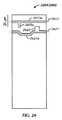
図44ないし55は、LTPSを使用する規範的ECB LCDディスプレイに向けられる。アモルファスシリコン(a−Si)を使用するECB LCDディスプレイ(図11ないし24に示す)と同様に、LTPSを使用するECB LCDディスプレイを製造するプロセスは、y方向にピクセルの蓄積キャパシタを接続するyVcomラインを形成するように、ビア及び付加的なM2ラインを構成することを含む。 Figures 44 through 55 are directed to an example ECB LCD display using LTPS. Similar to an ECB LCD display using amorphous silicon (a-Si) (shown in FIGS. 11-24), the process of manufacturing an ECB LCD display using LTPS is based on the yVcom line connecting pixel storage capacitors in the y direction. Forming vias and additional M2 lines to form.
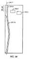
本発明の実施形態により、LTPSを使用するECB LCDディスプレイを製造する規範的プロセスを、図44ないし50を参照して以下に説明する。図44は、ポリSiの半導体層を示す。図45は、金属の第1層(M1)を示す。図46は、4601及び4602を含む接続部を示す。図47は、第2の金属層(M2)を示す。接続4601及び4602は、M1及びM2層を接続して、図示されたyVcomラインを形成する。図48ないし50は、接続層、反射層、及びITO層を各々示す。図51は、y方向の接続を許すyVcom部分を含む完成したピクセルを示している。図52は、図52に示す上面図に示された線に沿ったピクセル5101の側面図である。図53は、ピクセル5101の蓄積キャパシタンスの計算を示す。図54は、yVcomラインを含まないピクセル5101及びピクセル5403のアパーチャー比推定を示す。図55は、ピクセルのアパーチャー比を等化する上で助けとなるように、M1、M2及び/又はITO層の部分のようなある程度の金属をシフトできることを示す。 An exemplary process for manufacturing an ECB LCD display using LTPS according to embodiments of the present invention is described below with reference to FIGS. FIG. 44 shows a poly-Si semiconductor layer. FIG. 45 shows the first layer of metal (M1). FIG. 46 shows a connection including 4601 and 4602. FIG. 47 shows the second metal layer (M2).
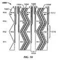
図56は、本発明の実施形態による接地セパレータ領域を含む規範的タッチスクリーン5600の一部分を示す。上述した幾つかの実施形態と同様に、タッチスクリーン5600は、ドライブのための領域(5601及び5602)及びセンスのための領域(5603及び5604)を含む。ドライブ領域は、ドライブ線5611及び5612に接続され、そしてセンス領域は、センス線5613及び5614に接続される。又、タッチスクリーンは、接地セパレータ領域5605も含み、これは、上述したように接地された一緒にリンクされた蓄積キャパシタを有するピクセルの領域である。接地セパレータ領域5605h、タッチピクセルエリアを電気的に分離する上で役立ち、タッチスクリーン5600によるタッチの検出を改善することができる。接地セパレータ領域は、例えば、タッチスクリーン全体に均一に離間させることができる。 FIG. 56 illustrates a portion of an
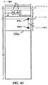
図57は、図56のA−A線に沿った側面図で、カバー5701、接着剤5702、偏光板5703、高抵抗(R)シールド5704、カラーフィルタガラス5705、ドライブ領域5601及び5602、センス領域5603及び5604、接地セパレータ領域5605、TFTガラス5706及び第2の偏光板5707を含むタッチスクリーン5600の一部分を示す。高Rシールド5704のような高抵抗シールドは、例えば、IPS LCDピクセルを使用するタッチスクリーンに使用されてもよい。高Rシールドは、ディスプレイ付近の低周波数/DC電圧がディスプレイの動作を妨げるのを阻止する上で助けとなる。同時に、高Rシールドは、容量性タッチ感知に典型的に使用されるもののような高周波信号がこのシールドを貫通できるようにする。それ故、高Rシールドは、ディスプレイがタッチ事象を感知できるようにしながら、ディスプレイをシールドする上で助けとなる。高Rシールドは、例えば、非常に高抵抗の有機材料、カーボンナノチューブ、等で作られ、そして100メガΩ/平方から10ギガΩ/平方の範囲の抵抗値を有するものでよい。 FIG. 57 is a side view taken along line AA in FIG. 56, and shows a cover 5701, an adhesive 5702, a polarizing plate 5703, a high resistance (R)
図58は、本発明の実施形態による規範的タッチスクリーン5800の一部分の側面図である。タッチスクリーン5800は、カラーフィルタガラス5801と、ピクセル層5803(図59に示すように、レッド(R)、グリーン(G)及びブルー(B)ピクセルと、ブラックマスクのブラックマスク線を含む)と、を含む。又、タッチスクリーン5800は、ブラックマスク線の下に金属線5805も含む。金属線5805は、例えば、ピクセルの領域とタッチスクリーンの境界におけるバスラインとの間に低抵抗経路を与えることができる。例えば、従来のLCD非IPSディスプレイでは、典型的にCFガラス上にある共通電極は、ITOの1枚のシートである。それ故、この共通電極の抵抗は、非常に低い。例えば、従来のLCDは、抵抗が約100Ω/平方のITOの共通電極を有する。しかしながら、上述した幾つかの実施形態では、共通電極は、比較的細い経路を通して共有の共通ラインに接続された領域へと「分解」される。ピクセルの領域と、共有の共通電極ラインとの間の接続は、特に、共有の共通ラインが存在するタッチスクリーンの境界からその領域が更に離れている場合には、比較的高い抵抗をもつことになる。金属線5805は、このような領域への経路の抵抗を下げる上で助けとなる。ブラックマスクの下に金属線5805を配置することで、例えば、ピクセルのアパーチャー比に対する金属線の影響を減少することができる。 FIG. 58 is a side view of a portion of an
図59は、本発明の実施形態による規範的なブラックマスクレイアウトである。ブラックマスク5901は、yVcomライン及びカラーデータラインをシールドする。又、マスク5901は、異なる領域間の潜在的なLCDアーティファクトを減少する上で助けとなる。マスク5902は、カラーデータラインをシールドする。2つのラインをカバーするマスク5901は、マスク5902より広い。 FIG. 59 is an exemplary black mask layout according to an embodiment of the present invention. The
図60は、ピクセル領域が複数の機能を果たす規範的なIPSベースのタッチ感知ディスプレイを示す。例えば、ピクセル領域は、あるときにはドライブ領域として動作し、別のときにはセンス領域として動作することができる。図60は、2つの形式のピクセル領域、即ちピクセル領域形式A及びピクセル領域形式Bを示す。第1の時間周期中には、A形式のピクセル領域、即ちタッチ列を刺激波形で駆動することができ、一方、B形式のピクセル領域、即ちタッチ行の各々のキャパシタンスを感知することができる。次の時間周期中には、B形式のピクセル領域、即ちタッチ行を刺激波形で駆動することができ、一方、A形式のピクセル領域、即ちタッチ列の各々のキャパシタンスを感知することができる。このプロセスを繰り返すことができる。2つのタッチ感知周期は約2msである。刺激波形は、種々の形態をとることができる。ある実施形態では、DCオフセットがゼロの約5Vピーク・ピークの正弦波である。他の時間周期及び波形を使用してもよい。 FIG. 60 shows an exemplary IPS-based touch-sensitive display where the pixel area serves multiple functions. For example, a pixel region can operate as a drive region at one time and a sense region at another. FIG. 60 shows two types of pixel regions: pixel region format A and pixel region format B. During the first time period, an A-type pixel region, i.e., a touch column, can be driven with a stimulus waveform, while a capacitance of each of the B-type pixel regions, i.e., touch rows, can be sensed. During the next time period, the B-type pixel region, i.e., the touch row, can be driven with a stimulus waveform, while the capacitance of each A-type pixel region, i.e., the touch column, can be sensed. This process can be repeated. The two touch sensing periods are about 2 ms. The stimulation waveform can take various forms. In one embodiment, a sine wave of approximately 5V peak-to-peak with a DC offset of zero. Other time periods and waveforms may be used.
図61は、上述した本発明の1つ以上の実施形態を含む規範的なコンピューティングシステム6100を示す。このコンピューティングシステム6100は、1つ以上のパネルプロセッサ6102及び周辺機器6104と、パネルサブシステム6106とを備えることができる。周辺機器6104は、ランダムアクセスメモリ(RAM)又は他の形式のメモリ又は記憶装置、ウオッチドッグタイマー、等を含むが、これに限定されない。パネルサブシステム6106は、1つ以上のセンスチャンネル6108、チャンネルスキャンロジック6110、及びドライバロジック6114を含むが、これに限定されない。チャンネルスキャンロジック6110は、RAM6112にアクセスし、センスチャンネルからデータを自動的に読み取り、そしてセンスチャンネルに対する制御を与える。更に、チャンネルスキャンロジック6110は、タッチスクリーン6124のドライブ線に選択的に適用できる種々の周波数及び位相において刺激信号6116を発生するようにドライバロジック6114を制御することができる。ある実施形態では、パネルサブシステム6106、パネルプロセッサ6102及び周辺機器6104は、単一の特定用途向け集積回路(ASIC)へ合体することができる。 FIG. 61 illustrates an
タッチスクリーン6124は、本発明の実施形態により複数のドライブ領域及び複数のセンス領域を有する容量性感知媒体を含むことができる。ドライブ領域及びセンス領域の各交点は、容量性感知ノードを表し、そしてタッチの「映像」を捕獲するものとしてタッチスクリーン6124が見られるときに特に有用な画素(ピクセル)6126として見ることができる。(換言すれば、タッチスクリーンの各タッチセンサにおいてタッチ事象が検出されたかどうかパネルサブシステム6106が決定した後、タッチ事象が生じたマルチタッチパネルにおけるタッチセンサのパターンをタッチの「映像」(例えば、パネルにタッチする指のパターン)として見ることができる。)タッチスクリーン6124の各センス領域は、パネルサブシステム6106におけるセンスチャンネル6108(事象検出及び復調回路とも称される)を駆動することができる。 The touch screen 6124 may include a capacitive sensing medium having a plurality of drive regions and a plurality of sense regions according to an embodiment of the present invention. Each intersection of the drive and sense regions represents a capacitive sensing node and can be viewed as a particularly useful pixel 6126 when the touch screen 6124 is viewed as capturing a “picture” of the touch. (In other words, after the panel subsystem 6106 determines whether or not a touch event has been detected in each touch sensor of the touch screen, the touch sensor pattern on the multi-touch panel in which the touch event has occurred is represented by a touch “image” (for example, a panel Each sense region of the touch screen 6124 can drive a sense channel 6108 (also referred to as an event detection and demodulation circuit) in the panel subsystem 6106.
又、コンピューティングシステム6100は、パネルプロセッサ6102から出力を受け取りそしてその出力に基づいてアクションを遂行するためのホストプロセッサ6128も備え、そのアクションは、カーソル又はポインタのような物体を移動し、スクロール又はパンを行い、制御設定を調整し、ファイル又はドキュメントをオープンし、メニューを見、選択を行い、インストラクションを実行し、ホスト装置に結合された周辺装置を操作し、電話コールに応答し、電話コールを発信し、電話コールを終了し、ボリューム又は音声設定を変更し、住所、頻繁にダイヤルされる番号、受信したコール、逸したコールのような電話通信に関連した情報を記憶し、コンピュータ又はコンピュータネットワークへログし、コンピュータ又はコンピュータネットワークの限定エリアへの許可された個々のアクセスを行えるようにし、コンピュータデスクトップのユーザの好ましい構成に関連したユーザプロフィールをロードし、ウェブコンテンツへのアクセスを許し、特定のプログラムを起動し、メッセージを暗号化又はデコードし、等々を含むが、これに限定されない。又、ホストプロセッサ6128は、パネル処理に関連しない付加的な機能を遂行できると共に、プログラム記憶装置6132と、装置のユーザにUIを与えるLCDディスプレイのようなディスプレイ装置6130とに結合することができる。このディスプレイ装置6130は、タッチスクリーン6124の下に部分的に又は完全に配置されたときに、このタッチスクリーンと共に、タッチスクリーン6118を形成することができる。 The
上述した機能の1つ以上は、メモリ(例えば、図61の周辺機器6104の1つ)に記憶されてパネルプロセッサ6102により実行されるファームウェア、又はプログラム記憶装置6132に記憶されてホストプロセッサ6128により実行されるファームウェアによって遂行できることに注意されたい。又、このファームウェアは、インストラクション実行システム、装置又はデバイスからインストラクションをフェッチして、インストラクションを実行できるコンピュータベースのシステム、プロセッサ収容システム又は他のシステムのようなインストラクション実行システム、装置又はデバイスにより又はそれに関連して使用するためにコンピュータ読み取り可能な媒体内に記憶し及び/又はその中で搬送することができる。本書において、「コンピュータ読み取り可能な媒体」とは、インストラクション実行システム、装置又はデバイスにより又はそれに関連して使用するためにプログラムを収容し又は記憶することのできる媒体である。コンピュータ読み取り可能な媒体は、電子、磁気、光学、電磁、赤外線、又は半導体システム、装置又はデバイス、ポータブルコンピュータディスケット(磁気)、ランダムアクセスメモリ(RAM)(磁気)、リードオンリメモリ(ROM)(磁気)、消去可能なプログラマブルリードオンリメモリ(EPROM)(磁気)、CD、CD−R、CD−RW、DVD、DVD−R又はDVD−RWのようなポータブル光学ディスク、或いはコンパクトフラッシュカード、セキュアなデジタルカード、USBメモリデバイス、メモリスティック、等のフラッシュメモリを含むが、これに限定されない。 One or more of the functions described above may be stored in memory (eg, one of the peripherals 6104 in FIG. 61) and executed by the
又、ファームウェアは、インストラクション実行システム、装置又はデバイスからインストラクションをフェッチして、インストラクションを実行できるコンピュータベースのシステム、プロセッサ収容システム又は他のシステムのようなインストラクション実行システム、装置又はデバイスにより又はそれに関連して使用するために、搬送媒体内で搬送することもできる。本書において、「搬送媒体」とは、インストラクション実行システム、装置又はデバイスにより又はそれに関連して使用するためにプログラムを通信し、伝播し又は搬送することのできる媒体である。読み取り可能な搬送媒体は、電子、磁気、光学、電磁又は赤外線のワイヤード又はワイヤレス伝播媒体を含むが、これに限定されない。 Firmware may also be by or related to an instruction execution system, apparatus or device such as a computer-based system, processor containing system or other system that can fetch instructions from the instruction execution system, apparatus or device and execute the instructions. It can also be transported in a transport medium for use. In this document, a “carrier medium” is a medium on which a program can be communicated, propagated or carried for use by or in connection with an instruction execution system, apparatus or device. Readable carrier media include, but are not limited to, electronic, magnetic, optical, electromagnetic or infrared wired or wireless propagation media.
図62aは、タッチスクリーン6224及びディスプレイ装置6230を備えた規範的移動電話6236を示し、タッチスクリーンは、本発明の実施形態による二重機能容量性素子を伴うピクセルを含むものである。 FIG. 62a shows an exemplary
図62bは、タッチスクリーン6224及びディスプレイ装置6230を備えた規範的デジタルメディアプレーヤ6240を示し、タッチスクリーンは、本発明の実施形態による二重機能容量性素子を伴うピクセルを含むものである。 FIG. 62b shows an exemplary
図62cは、タッチスクリーン(トラックパッド)6224及びディスプレイ6230を備えた規範的パーソナルコンピュータ6244を示し、(ディスプレイがタッチスクリーンの一部分である実施形態では)パーソナルコンピュータのタッチスクリーンは、二重機能容量性素子を伴うピクセルを含むものである。 FIG. 62c shows an exemplary
以上、添付図面を参照して、本発明の実施形態を充分に説明したが、当業者であれば、種々の変更や修正が明らかであろう。 Although the embodiments of the present invention have been fully described with reference to the accompanying drawings, various changes and modifications will be apparent to those skilled in the art.
100:LCDディスプレイ(パネル)
101、102、103、104:ピクセル
105、155:薄膜トランジスタ(TFT)
105a、155a:ゲート
105b、155b:ソース
105c、155c:ドレイン
107、157:蓄積キャパシタ
107a、157a:上部電極
107b、157b:下部電極
109、159:液晶キャパシタ
109a、159a:ピクセル電極
109b、159b:共通電極
121:xVcom
123:yVcom
127:接続部
131、133:切断部
161:カラーフィルタ電圧源
201、205、207:領域
213:タッチ回路
215:タッチASIC
217:スイッチ回路
250:導電性ドット
251、255、257:領域
301、303:ピクセル
307、309:TFT
311、312:ゲートライン
313、314:データライン
315、316:xVcomライン
319、321:フリンジ電界電極
323、325:蓄積キャパシタ
326:電荷増幅器
327:指
600:タッチスクリーン
602:フレックス回路
604、606:金属トレース
614:食い違った縁
616:ノッチ
900:タッチスクリーン
902:多角形領域(レンガ)
906:列
910:バスライン
1000:ジグザグ二重補間タッチスクリーン
1002:多角形領域(五角形)
1004:センス(又はドライブ)領域
1006:接地ガード
1010:チャンネル
1101、1102:ピクセル
5601:ドライブ
5602:ドライブ
5603:センス
5604:センス
5605:均一スペースセパレータ
5611:ドライブ
5612:ドライブ
5701:カバー
5702:接着剤
5703:偏光板
5704:高Rシールド
5705:CFガラス
5706:TFTガラス
5707:第2偏光板
5713:センス
5714:センス
6100:コンピューティングシステム
6102:パネルプロセッサ
6104:周辺装置
6106:パネルサブシステム
6108:センスチャンネル
6110:チャンネルスキャンロジック
6112:RAM
6114:ドライバロジック
6115:電荷ポンプ
6124:タッチスクリーン
6128:ホストプロセッサ
6132:プログラム記憶装置
6224:タッチセンサパネル
6230:ディスプレイ装置
6236:移動電話
6240:メディアプレーヤ
6244:パーソナルコンピュータ100: LCD display (panel)
101, 102, 103, 104:
105a, 155a:
123: yVcom
127:
217: Switch circuit 250:
311, 312:
906: Row 910: Bus line 1000: Zigzag double interpolation touch screen 1002: Polygonal region (pentagon)
1004: Sense (or drive) area 1006: Ground guard 1010:
6114: Driver logic 6115: Charge pump 6124: Touch screen 6128: Host processor 6132: Program storage device 6224: Touch sensor panel 6230: Display device 6236: Mobile phone 6240: Media player 6244: Personal computer
Claims (58)
Translated fromJapanese複数の隣接する表示ピクセルにおける容量性素子を接続する複数の第1の共通電圧ラインと、
2つ以上の第1の共通電圧ラインを接続する第2の共通電圧ラインと、
を備えたタッチスクリーン。In a touch screen comprising display pixels with capacitive elements,
A plurality of first common voltage lines connecting capacitive elements in a plurality of adjacent display pixels;
A second common voltage line connecting two or more first common voltage lines;
With touch screen.
表示ピクセルの複数領域を備え、各領域の容量性素子は、(i)第1の共通電圧ライン及び第2の共通電圧ラインのグリッドと一緒に電気的接続され、そして(ii)グリッドの切断部により他の領域から電気的に分離される、タッチスクリーン。In a touch screen comprising display pixels with capacitive elements,
A plurality of regions of display pixels, wherein the capacitive elements in each region are (i) electrically connected together with a grid of first common voltage lines and second common voltage lines, and (ii) grid cuts A touch screen that is electrically isolated from other areas by the touch screen.
刺激信号により刺激される表示ピクセルのドライブ領域と、
前記刺激信号に対応するセンス信号を受信する表示ピクセルのセンス領域と、
接地された表示ピクセルの接地領域と、
を備え、各領域の容量性素子は、(i)第1の共通電圧ライン及び第2の共通電圧ラインにより一緒に電気的接続され、そして(ii)グリッドの切断部により他の領域から電気的に分離される、タッチスクリーン。In a touch screen comprising display pixels with capacitive elements,
A drive region of the display pixel stimulated by the stimulus signal;
A sense region of a display pixel that receives a sense signal corresponding to the stimulus signal;
A ground area of a grounded display pixel; and
The capacitive elements in each region are (i) electrically connected together by a first common voltage line and a second common voltage line, and (ii) electrically connected from other regions by a grid cut Separated into a touch screen.
タッチスクリーンの表面の第1の側に配置されて、その表面の第2の側へ電界を発散させる容量性素子を含む表示ピクセルのドライブ領域と、
前記表面の第1の側に配置されて、その表面の第2の側から電界を受け取る容量性素子を含む表示ピクセルのセンス領域と、
前記表面の第2の側からの電界が、前記センス領域により受け取られる前にシールド層を通過するように配置された実質的に高い抵抗材料で形成されたシールド層と、
を備えたタッチスクリーン。In a touch screen comprising display pixels with capacitive elements,
A display pixel drive region including a capacitive element disposed on a first side of the surface of the touch screen and dissipating an electric field to the second side of the surface;
A sense region of a display pixel disposed on a first side of the surface and including a capacitive element that receives an electric field from the second side of the surface;
A shield layer formed of a substantially high resistance material disposed such that an electric field from the second side of the surface passes through the shield layer before being received by the sense region;
With touch screen.
刺激信号により刺激される表示ピクセルのドライブ領域と、
前記刺激信号に対応するセンス信号を受信する表示ピクセルのセンス領域と、
ブラックマスク線と、
前記ブラックマスク線の下の導電性ラインと、
を備えたタッチスクリーン。In a touch screen comprising display pixels with capacitive elements,
A drive region of the display pixel stimulated by the stimulus signal;
A sense region of a display pixel that receives a sense signal corresponding to the stimulus signal;
Black mask lines,
A conductive line under the black mask line;
With touch screen.
2つ以上の第1の共通電圧ラインを接続する第2の共通電圧ラインと、
を含むタッチスクリーンを備えた移動電話。A plurality of first common voltage lines connecting capacitive elements in a plurality of adjacent display pixels;
A second common voltage line connecting two or more first common voltage lines;
Mobile phone with touch screen including.
2つ以上の第1の共通電圧ラインを接続する第2の共通電圧ラインと、
を含むタッチスクリーンを備えたデジタルメディアプレーヤ。A plurality of first common voltage lines connecting capacitive elements in a plurality of adjacent display pixels;
A second common voltage line connecting two or more first common voltage lines;
A digital media player with a touch screen including:
表示段階中に容量性素子を動作してタッチスクリーンに映像を発生するステップと、
タッチ段階中に容量性素子を動作してタッチスクリーン上又はその付近のタッチ事象を感知するステップと、
を備え、前記タッチ段階は、刺激信号を容量性素子へ送信すること及び容量性素子からセンス信号を受信することの少なくとも1つを含む、方法。In a method of operating a touch screen including display pixels with capacitive elements,
Operating the capacitive element during the display phase to generate an image on the touch screen; and
Sensing a touch event on or near a touch screen by operating a capacitive element during a touch phase; and
And wherein the touching step comprises at least one of transmitting a stimulation signal to the capacitive element and receiving a sense signal from the capacitive element.
ピクセルのドライブ領域における容量性素子を刺激信号で駆動する段階と、
前記ドライブ領域により発生される電界をピクセルのセンス領域における容量性素子で感知する段階と、
を含む請求項39に記載の方法。The step of operating the capacitive element during the touch phase comprises:
Driving a capacitive element in the drive region of the pixel with a stimulus signal;
Sensing an electric field generated by the drive region with a capacitive element in a sense region of a pixel;
40. The method of claim 39, comprising:
ドライブ領域における容量性素子を通して交流(AC)信号を送信する段階を含み、このAC信号は、表示段階中に容量性素子を通して送信されるLCD反転信号と同じ直流(DC)オフセットを有する、請求項39に記載の方法。The step of operating the capacitive element during the touch phase comprises:
Transmitting an alternating current (AC) signal through the capacitive element in the drive region, the AC signal having the same direct current (DC) offset as the LCD inverted signal transmitted through the capacitive element during the display phase. 40. The method according to 39.
ドライブ領域を接続する共通ラインを通して反転信号を送信して、ドライブ領域のピクセルにおける液晶のLCD反転を遂行することを含む、請求項39に記載の方法。The step of operating the capacitive element during the display phase comprises:
40. The method of claim 39, comprising transmitting an inversion signal through a common line connecting the drive areas to perform LCD inversion of the liquid crystal in the pixels of the drive area.
複数の隣接する表示ピクセルにおける容量性素子を接続する複数の第1の共通電圧ラインを形成するステップと、
2つ以上の第1の共通電圧ライン接続する第2の共通電圧ライン形成するステップと、
を備えた方法。In a method of manufacturing a touch screen,
Forming a plurality of first common voltage lines connecting capacitive elements in a plurality of adjacent display pixels;
Forming a second common voltage line connecting two or more first common voltage lines;
With a method.
第1の共通電圧ラインを含む導電性材料の第1層を形成する段階を含む、請求項29に記載の方法。The step of forming a plurality of first common voltage lines comprises:
30. The method of claim 29, comprising forming a first layer of conductive material that includes a first common voltage line.
第1の共通電圧ラインを一緒に接続する第2の共通電圧ラインの下部を形成する段階、
不動態化層を形成する段階、
不動態化層にビアを形成する段階、及び
第2の共通電圧ラインの上部を含む導電性材料の第2層を形成する段階であって、前記上部をビアに接続して、第2の共通電圧ラインを形成する段階、
を備えた請求項29に記載の方法。Said step of forming a second common voltage line comprises:
Forming a lower portion of a second common voltage line connecting together the first common voltage line;
Forming a passivation layer,
Forming a via in the passivation layer, and forming a second layer of conductive material including an upper portion of a second common voltage line, the upper portion being connected to the via, and a second common Forming a voltage line;
30. The method of claim 29 comprising:
容量性素子のグループを電気的に分離して複数のピクセル領域を形成する切断部を含むように、複数の第1の共通電圧ライン及び複数の第2の共通電圧ラインを形成するステップであって、領域内のピクセルの全ての容量性素子を一緒に電気的接続するようなステップを更に備えた、請求項29に記載の方法。A plurality of second common voltage lines are formed, the method further comprising:
Forming a plurality of first common voltage lines and a plurality of second common voltage lines so as to include a cutting portion for electrically separating a group of capacitive elements to form a plurality of pixel regions. 30. The method of claim 29, further comprising the step of electrically connecting all capacitive elements of the pixels in the region together.
Applications Claiming Priority (5)
| Application Number | Priority Date | Filing Date | Title |
|---|---|---|---|
| US7833708P | 2008-07-03 | 2008-07-03 | |
| US61/078,337 | 2008-07-03 | ||
| US12/240,964US8508495B2 (en) | 2008-07-03 | 2008-09-29 | Display with dual-function capacitive elements |
| US12/240,964 | 2008-09-29 | ||
| PCT/US2009/049313WO2010002929A2 (en) | 2008-07-03 | 2009-06-30 | Display with dual-function capacitive elements |
Related Child Applications (1)
| Application Number | Title | Priority Date | Filing Date |
|---|---|---|---|
| JP2013185517ADivisionJP5719893B2 (en) | 2008-07-03 | 2013-09-06 | Display with dual function capacitive element |
Publications (1)
| Publication Number | Publication Date |
|---|---|
| JP2011527787Atrue JP2011527787A (en) | 2011-11-04 |
Family
ID=41258831
Family Applications (2)
| Application Number | Title | Priority Date | Filing Date |
|---|---|---|---|
| JP2011516828APendingJP2011527787A (en) | 2008-07-03 | 2009-06-30 | Display with dual function capacitive element |
| JP2013185517AExpired - Fee RelatedJP5719893B2 (en) | 2008-07-03 | 2013-09-06 | Display with dual function capacitive element |
Family Applications After (1)
| Application Number | Title | Priority Date | Filing Date |
|---|---|---|---|
| JP2013185517AExpired - Fee RelatedJP5719893B2 (en) | 2008-07-03 | 2013-09-06 | Display with dual function capacitive element |
Country Status (7)
| Country | Link |
|---|---|
| US (5) | US8508495B2 (en) |
| EP (1) | EP2141573B1 (en) |
| JP (2) | JP2011527787A (en) |
| KR (5) | KR101275460B1 (en) |
| CN (3) | CN103870088B (en) |
| AU (1) | AU2009267044B2 (en) |
| WO (1) | WO2010002929A2 (en) |
Cited By (17)
| Publication number | Priority date | Publication date | Assignee | Title |
|---|---|---|---|---|
| JP2013122752A (en)* | 2011-12-09 | 2013-06-20 | Lg Display Co Ltd | Touch screen integrated display device |
| WO2013094527A1 (en)* | 2011-12-19 | 2013-06-27 | シャープ株式会社 | Touch sensor-embedded display panel, display device provided therewith, and method for driving touch sensor-embedded display panel |
| JP2013232189A (en)* | 2012-04-27 | 2013-11-14 | Koutatsu Ryu | Touch device |
| WO2013175726A1 (en)* | 2012-05-25 | 2013-11-28 | パナソニック液晶ディスプレイ株式会社 | Liquid crystal display device |
| JP2014086072A (en)* | 2012-10-23 | 2014-05-12 | Lg Display Co Ltd | Display device and driving method thereof |
| JP2014089269A (en)* | 2012-10-29 | 2014-05-15 | Dainippon Printing Co Ltd | Optical laminate for front surface of in-cell touch panel liquid crystal element, and in-cell touch panel liquid crystal display device, and manufacturing method of the same |
| WO2015170677A1 (en)* | 2014-05-08 | 2015-11-12 | シャープ株式会社 | Method for manufacturing position input device |
| WO2015182473A1 (en)* | 2014-05-28 | 2015-12-03 | シャープ株式会社 | Touch panel device |
| JP2016503548A (en)* | 2012-11-27 | 2016-02-04 | ガーディアン インダストリーズ コーポレイションGuardian Industries Corp. | Projected capacitive touch panel including a silver-containing transparent conductive layer |
| JP2016518651A (en)* | 2013-03-25 | 2016-06-23 | 合肥京東方光電科技有限公司 | Built-in capacitive touch panel and display device |
| JP2016146183A (en)* | 2009-05-13 | 2016-08-12 | シナプティクス インコーポレイテッド | Capacitance sensor device |
| WO2016136664A1 (en)* | 2015-02-24 | 2016-09-01 | シャープ株式会社 | Liquid crystal display device with touch sensor |
| US9483987B2 (en) | 2012-02-20 | 2016-11-01 | Panasonic Liquid Crystal Display Co., Ltd. | Embedded touch screen |
| JP2017504139A (en)* | 2014-01-28 | 2017-02-02 | 京東方科技集團股▲ふん▼有限公司Boe Technology Group Co.,Ltd. | In-cell touch panel and display device |
| JP2017054141A (en)* | 2016-11-16 | 2017-03-16 | 大日本印刷株式会社 | Optical laminate for front surface of in-cell touch panel liquid crystal element, and in-cell touch panel liquid crystal display device, and manufacturing method of the same |
| US9760221B2 (en) | 2012-05-28 | 2017-09-12 | Panasonic Liquid Crystal Display Co., Ltd. | Embedded touch screen |
| JP2018530822A (en)* | 2015-10-02 | 2018-10-18 | シャープ株式会社 | touch screen |
Families Citing this family (232)
| Publication number | Priority date | Publication date | Assignee | Title |
|---|---|---|---|---|
| KR101407372B1 (en)* | 2006-07-11 | 2014-06-17 | 코닌클리케 필립스 엔.브이. | Improved electrode layout for display |
| US8547114B2 (en) | 2006-11-14 | 2013-10-01 | Cypress Semiconductor Corporation | Capacitance to code converter with sigma-delta modulator |
| US8633915B2 (en) | 2007-10-04 | 2014-01-21 | Apple Inc. | Single-layer touch-sensitive display |
| US20090174676A1 (en) | 2008-01-04 | 2009-07-09 | Apple Inc. | Motion component dominance factors for motion locking of touch sensor data |
| US8525798B2 (en) | 2008-01-28 | 2013-09-03 | Cypress Semiconductor Corporation | Touch sensing |
| US8319505B1 (en) | 2008-10-24 | 2012-11-27 | Cypress Semiconductor Corporation | Methods and circuits for measuring mutual and self capacitance |
| US8358142B2 (en)* | 2008-02-27 | 2013-01-22 | Cypress Semiconductor Corporation | Methods and circuits for measuring mutual and self capacitance |
| JP4816668B2 (en)* | 2008-03-28 | 2011-11-16 | ソニー株式会社 | Display device with touch sensor |
| US8508495B2 (en) | 2008-07-03 | 2013-08-13 | Apple Inc. | Display with dual-function capacitive elements |
| CN101320185B (en)* | 2008-07-18 | 2011-01-26 | 昆山龙腾光电有限公司 | Touch control type liquid crystal display array substrates and LCD device |
| JP5372630B2 (en)* | 2008-07-17 | 2013-12-18 | Nltテクノロジー株式会社 | Display device and driving method of display device |
| US20100059294A1 (en)* | 2008-09-08 | 2010-03-11 | Apple Inc. | Bandwidth enhancement for a touch sensor panel |
| US8624845B2 (en)* | 2008-09-26 | 2014-01-07 | Cypress Semiconductor Corporation | Capacitance touch screen |
| US8321174B1 (en) | 2008-09-26 | 2012-11-27 | Cypress Semiconductor Corporation | System and method to measure capacitance of capacitive sensor array |
| KR101268963B1 (en)* | 2008-10-30 | 2013-05-30 | 엘지디스플레이 주식회사 | Liquid Crystal Display |
| US8144295B2 (en) | 2008-11-18 | 2012-03-27 | Apple Inc. | Common bus design for a TFT-LCD display |
| US8749496B2 (en) | 2008-12-05 | 2014-06-10 | Apple Inc. | Integrated touch panel for a TFT display |
| US8922521B2 (en) | 2009-02-02 | 2014-12-30 | Apple Inc. | Switching circuitry for touch sensitive display |
| US8217913B2 (en) | 2009-02-02 | 2012-07-10 | Apple Inc. | Integrated touch screen |
| US9261997B2 (en)* | 2009-02-02 | 2016-02-16 | Apple Inc. | Touch regions in diamond configuration |
| US8760412B2 (en) | 2009-02-02 | 2014-06-24 | Apple Inc. | Dual configuration for display data lines |
| US7995041B2 (en)* | 2009-02-02 | 2011-08-09 | Apple Inc. | Integrated touch screen |
| US20100214247A1 (en)* | 2009-02-20 | 2010-08-26 | Acrosense Technology Co., Ltd. | Capacitive Touch Panel |
| TWI460639B (en)* | 2009-02-23 | 2014-11-11 | Innolux Corp | System for display images |
| US8686951B2 (en) | 2009-03-18 | 2014-04-01 | HJ Laboratories, LLC | Providing an elevated and texturized display in an electronic device |
| US8643624B2 (en)* | 2009-03-18 | 2014-02-04 | Synaptics Incorporated | Capacitive sensing using a segmented common voltage electrode of a display |
| US8593410B2 (en) | 2009-04-10 | 2013-11-26 | Apple Inc. | Touch sensor panel design |
| US8355887B1 (en) | 2009-04-24 | 2013-01-15 | Cypress Semiconductor Corporation | Proximity based gesturing devices, systems and methods |
| US8279194B2 (en)* | 2009-05-22 | 2012-10-02 | Elo Touch Solutions, Inc. | Electrode configurations for projected capacitive touch screen |
| US20100295813A1 (en)* | 2009-05-22 | 2010-11-25 | Tyco Electronics Corporation | System and method for a projected capacitive touchscreen having grouped electrodes |
| US8456586B2 (en) | 2009-06-11 | 2013-06-04 | Apple Inc. | Portable computer display structures |
| EP2300900B1 (en)* | 2009-06-24 | 2018-09-05 | Microchip Technology Germany GmbH | Electrode arrangement for display device |
| US8957874B2 (en) | 2009-06-29 | 2015-02-17 | Apple Inc. | Touch sensor panel design |
| US8723827B2 (en) | 2009-07-28 | 2014-05-13 | Cypress Semiconductor Corporation | Predictive touch surface scanning |
| US9069405B2 (en) | 2009-07-28 | 2015-06-30 | Cypress Semiconductor Corporation | Dynamic mode switching for fast touch response |
| US8477106B2 (en)* | 2009-07-29 | 2013-07-02 | Elo Touch Solutions, Inc. | System and method for a projected capacitive touchscreen having weight based coordinate determination |
| KR101073684B1 (en)* | 2009-08-25 | 2011-10-14 | 주식회사 지니틱스 | Transparent Electrode Pattern Of Capacitive Touch Screen For Low Resistance |
| US8842079B2 (en)* | 2009-10-09 | 2014-09-23 | Egalax—Empia Technology Inc. | Method and device for determining a touch or touches |
| US8408780B2 (en)* | 2009-11-03 | 2013-04-02 | Apple Inc. | Portable computer housing with integral display |
| US8743309B2 (en) | 2009-11-10 | 2014-06-03 | Apple Inc. | Methods for fabricating display structures |
| KR20110054725A (en)* | 2009-11-18 | 2011-05-25 | 엘지디스플레이 주식회사 | LCD Display |
| US8598555B2 (en)* | 2009-11-20 | 2013-12-03 | Authentec, Inc. | Finger sensing apparatus with selectively operable transmitting/receiving pixels and associated methods |
| US20110134050A1 (en)* | 2009-12-07 | 2011-06-09 | Harley Jonah A | Fabrication of touch sensor panel using laser ablation |
| US20110134051A1 (en)* | 2009-12-08 | 2011-06-09 | Holylite Microelectronics Corp. | Liquid crystal display system integrated with touch detector |
| CN101840293B (en)* | 2010-01-21 | 2012-03-21 | 宸鸿科技(厦门)有限公司 | Scanning method for projected capacitive touch panels |
| JP5484097B2 (en)* | 2010-01-27 | 2014-05-07 | 株式会社ワコム | Position detection apparatus and method |
| US20110199342A1 (en) | 2010-02-16 | 2011-08-18 | Harry Vartanian | Apparatus and method for providing elevated, indented or texturized sensations to an object near a display device or input detection using ultrasound |
| CN102884496B (en)* | 2010-02-26 | 2017-06-30 | 辛纳普蒂克斯公司 | Modify demodulation to avoid interference |
| US9146644B2 (en)* | 2010-03-08 | 2015-09-29 | Nuvoton Technology Corporation | Systems and methods for detecting multiple touch points in surface-capacitance type touch panels |
| KR101307962B1 (en) | 2010-03-19 | 2013-09-12 | 엘지디스플레이 주식회사 | In-plane switching mode liquid crystal display device having touch sensing function and method of fabricating the same |
| KR101298234B1 (en) | 2010-03-19 | 2013-08-22 | 엘지디스플레이 주식회사 | In-plane switching mode liquid crystal display device having touch sensing function and method of fabricating the same |
| US8803862B2 (en)* | 2010-03-22 | 2014-08-12 | Apple Inc. | Gamma resistor sharing for VCOM generation |
| KR101735297B1 (en)* | 2010-03-30 | 2017-05-16 | (주)멜파스 | Panel and device for sensing touch input |
| KR101113467B1 (en)* | 2010-04-01 | 2012-02-29 | 삼성모바일디스플레이주식회사 | Touch Screen Panel |
| TWI544458B (en)* | 2010-04-02 | 2016-08-01 | 元太科技工業股份有限公司 | Display panel |
| WO2011132346A1 (en)* | 2010-04-22 | 2011-10-27 | シャープ株式会社 | Display device |
| US9898121B2 (en) | 2010-04-30 | 2018-02-20 | Synaptics Incorporated | Integrated capacitive sensing and displaying |
| US9727175B2 (en) | 2010-05-14 | 2017-08-08 | Elo Touch Solutions, Inc. | System and method for detecting locations of touches on a projected capacitive touch sensor |
| JP2013526746A (en) | 2010-05-14 | 2013-06-24 | イーロ・タッチ・ソリューションズ・インコーポレイテッド | System and method for detecting the position of a touch on a touch sensor |
| CN102243553B (en)* | 2010-05-16 | 2015-06-10 | 宸鸿科技(厦门)有限公司 | Capacitive touch panel and method for reducing visuality of metal conductor of capacitive touch panel |
| US9335870B2 (en)* | 2010-06-07 | 2016-05-10 | Apple Inc. | Touch-display crosstalk |
| US9652088B2 (en) | 2010-07-30 | 2017-05-16 | Apple Inc. | Fabrication of touch sensor panel using laser ablation |
| CN103052928B (en) | 2010-08-04 | 2015-12-16 | 惠普发展公司,有限责任合伙企业 | Systems and methods enabling multiple display input |
| CN102576276B (en)* | 2010-08-23 | 2017-05-10 | 谱瑞科技股份有限公司 | Capacitive Scan Proximity Detection |
| KR101320109B1 (en)* | 2010-10-26 | 2013-10-18 | 엘지디스플레이 주식회사 | In-Cell Touch Panel For Flat Panel Display Device |
| US8467177B2 (en) | 2010-10-29 | 2013-06-18 | Apple Inc. | Displays with polarizer windows and opaque masking layers for electronic devices |
| US9143668B2 (en) | 2010-10-29 | 2015-09-22 | Apple Inc. | Camera lens structures and display structures for electronic devices |
| KR20120049019A (en)* | 2010-11-08 | 2012-05-16 | 삼성모바일디스플레이주식회사 | Capacitive touch panel |
| KR101770319B1 (en)* | 2010-11-25 | 2017-08-22 | 엘지디스플레이 주식회사 | Liquid crystal display device |
| KR101219273B1 (en)* | 2011-01-14 | 2013-01-08 | 삼성디스플레이 주식회사 | touch screen system |
| CN102650916B (en) | 2011-02-25 | 2014-11-26 | 乐金显示有限公司 | Touch sensor integrated display device |
| US10761358B2 (en)* | 2011-03-03 | 2020-09-01 | Apple Inc. | Display screen shield line system |
| US8743244B2 (en) | 2011-03-21 | 2014-06-03 | HJ Laboratories, LLC | Providing augmented reality based on third party information |
| KR101819677B1 (en)* | 2011-04-01 | 2018-01-17 | 엘지디스플레이 주식회사 | Touch sensor integrated type display device |
| JP5759813B2 (en)* | 2011-07-13 | 2015-08-05 | 株式会社ジャパンディスプレイ | Liquid crystal display |
| CN103733168B (en)* | 2011-07-22 | 2016-11-23 | 波利Ic有限及两合公司 | Capacitive Touch Area Device |
| US8907921B2 (en) | 2011-08-30 | 2014-12-09 | Synaptics Incorporated | Interference sensing within a display device with an integrated sensing device |
| JP5925896B2 (en) | 2011-09-07 | 2016-05-25 | シナプティクス インコーポレイテッド | Capacitive detection during hidden update time |
| US20130081869A1 (en)* | 2011-09-30 | 2013-04-04 | Jae Hong Kim | Touch sensing apparatus and method of manufacturing the same |
| US10261370B2 (en) | 2011-10-05 | 2019-04-16 | Apple Inc. | Displays with minimized border regions having an apertured TFT layer for signal conductors |
| US9286826B2 (en) | 2011-10-28 | 2016-03-15 | Apple Inc. | Display with vias for concealed printed circuit and component attachment |
| US9075488B2 (en) | 2011-11-03 | 2015-07-07 | Synaptics Incorporated | Virtual geometries for integrated display and sensing devices |
| US9176621B2 (en) | 2011-11-18 | 2015-11-03 | Synaptics Incorporated | Flexible timing and multiplexing for a display device comprising an integrated capacitive sensing device |
| KR101912832B1 (en) | 2011-11-24 | 2018-10-30 | 삼성디스플레이 주식회사 | Display device including optical sensor |
| KR101284331B1 (en)* | 2011-12-09 | 2013-07-08 | 성균관대학교산학협력단 | Recharge systen for green car and method thereof |
| CN103164062B (en)* | 2011-12-15 | 2016-05-25 | 瀚宇彩晶股份有限公司 | Touch panel and touch display device |
| US8970547B2 (en) | 2012-02-01 | 2015-03-03 | Synaptics Incorporated | Noise-adapting touch sensing window |
| KR20130115621A (en) | 2012-04-12 | 2013-10-22 | 삼성디스플레이 주식회사 | Display device and fabrication method of the same |
| US9329723B2 (en) | 2012-04-16 | 2016-05-03 | Apple Inc. | Reconstruction of original touch image from differential touch image |
| US9244572B2 (en)* | 2012-05-04 | 2016-01-26 | Blackberry Limited | Electronic device including touch-sensitive display and method of detecting touches |
| KR101361707B1 (en)* | 2012-05-07 | 2014-02-11 | 엘지디스플레이 주식회사 | Liquid crystal display and method of driving the same |
| US20130307810A1 (en)* | 2012-05-15 | 2013-11-21 | Chimei Innolux Corporation | Capacitive touch panel device |
| US9395583B2 (en) | 2012-06-06 | 2016-07-19 | Apple Inc. | Column spacer design for a display incorporating a third metal layer |
| TWI463374B (en) | 2012-06-07 | 2014-12-01 | Mstar Semiconductor Inc | Touch panel |
| JP6055206B2 (en)* | 2012-06-08 | 2016-12-27 | 株式会社ジャパンディスプレイ | Liquid crystal display |
| US8941640B2 (en)* | 2012-06-08 | 2015-01-27 | Apple Inc. | Differential VCOM resistance or capacitance tuning for improved image quality |
| US9001280B2 (en) | 2012-06-08 | 2015-04-07 | Apple Inc. | Devices and methods for shielding displays from electrostatic discharge |
| US9280231B2 (en) | 2012-06-20 | 2016-03-08 | Synaptics Incorporated | Disabling display lines during input sensing periods |
| KR101490703B1 (en)* | 2012-06-20 | 2015-02-06 | 엘지디스플레이 주식회사 | Liquid crystal display panel and liquid crystal display using the same |
| US9226347B2 (en) | 2012-06-25 | 2015-12-29 | Apple Inc. | Displays with vias |
| US9575599B1 (en) | 2012-07-17 | 2017-02-21 | Parade Technologies, Ltd. | Multi-touch ghost discrimination |
| US9182432B2 (en) | 2012-07-18 | 2015-11-10 | Synaptics Incorporated | Capacitance measurement |
| TW201407249A (en)* | 2012-08-10 | 2014-02-16 | Yan-Hong Du | Active electronic paper touch apparatus |
| US10073568B2 (en) | 2012-08-15 | 2018-09-11 | Synaptics Incorporated | System and method for interference avoidance for a display device comprising an integrated sensing device |
| US9214507B2 (en) | 2012-08-17 | 2015-12-15 | Apple Inc. | Narrow border organic light-emitting diode display |
| US8970546B2 (en) | 2012-08-31 | 2015-03-03 | Synaptics Incorporated | Method and apparatus for improved input sensing using a display processor reference signal |
| US9454025B2 (en) | 2012-08-31 | 2016-09-27 | Apple Inc. | Displays with reduced driver circuit ledges |
| US10073550B2 (en) | 2012-09-20 | 2018-09-11 | Synaptics Incorporated | Concurrent input sensing and display updating |
| US9557846B2 (en) | 2012-10-04 | 2017-01-31 | Corning Incorporated | Pressure-sensing touch system utilizing optical and capacitive systems |
| US9529462B2 (en)* | 2012-10-29 | 2016-12-27 | Sharp Kabushiki Kaisha | Touch panel |
| US9411474B2 (en) | 2012-11-15 | 2016-08-09 | Nokia Technologies Oy | Shield electrode overlying portions of capacitive sensor electrodes |
| CN103049156B (en)* | 2012-12-13 | 2015-12-23 | 北京京东方光电科技有限公司 | A kind of capacitance type in-cell touch panel and display device |
| KR102008739B1 (en)* | 2012-12-21 | 2019-08-09 | 엘지이노텍 주식회사 | Touch panel |
| US9336723B2 (en) | 2013-02-13 | 2016-05-10 | Apple Inc. | In-cell touch for LED |
| KR102074424B1 (en)* | 2013-03-04 | 2020-02-07 | 삼성디스플레이 주식회사 | Liquid crystal display and manufacturing method thereof |
| WO2014165063A1 (en)* | 2013-03-12 | 2014-10-09 | Cirque Corporation | Multiplexing and demultiplexing to reduce drive and sense electrodes for single layer touch sensors |
| US8970577B2 (en) | 2013-03-13 | 2015-03-03 | Synaptics Incorporated | Reducing display artifacts after non-display update periods |
| KR20140122395A (en) | 2013-04-10 | 2014-10-20 | 어보브반도체 주식회사 | Capacitive type touch panel |
| KR102214929B1 (en)* | 2013-04-15 | 2021-02-10 | 삼성전자주식회사 | Apparatus and method for providing tactile |
| WO2014207287A1 (en) | 2013-05-10 | 2014-12-31 | Nokia Corporation | Touch sensor array |
| US9140737B2 (en)* | 2013-05-21 | 2015-09-22 | Nokia Technologies Oy | Capacitive touch sensor |
| KR102038883B1 (en)* | 2013-05-22 | 2019-10-31 | 엘지디스플레이 주식회사 | Display device and driving method thereof |
| US9535544B2 (en)* | 2013-05-31 | 2017-01-03 | Apple Inc. | Reducing touch pixel coupling |
| US9715291B2 (en) | 2013-06-18 | 2017-07-25 | Synaptics Incorporated | Pre-charging a gate electrode before resuming display updating |
| US9152283B2 (en) | 2013-06-27 | 2015-10-06 | Synaptics Incorporated | Full in-cell sensor |
| KR102086098B1 (en)* | 2013-07-03 | 2020-03-09 | 삼성디스플레이 주식회사 | Display device |
| US9507472B2 (en) | 2013-07-10 | 2016-11-29 | Synaptics Incorporated | Hybrid capacitive baseline management |
| TWI507956B (en)* | 2013-07-17 | 2015-11-11 | Pixart Imaging Inc | Single-layer capacitive touch sensor |
| CN104346004B (en)* | 2013-07-29 | 2017-08-29 | 原相科技股份有限公司 | Single layer capacitive touch sensor |
| US9552089B2 (en) | 2013-08-07 | 2017-01-24 | Synaptics Incorporated | Capacitive sensing using a matrix electrode pattern |
| US9886141B2 (en) | 2013-08-16 | 2018-02-06 | Apple Inc. | Mutual and self capacitance touch measurements in touch panel |
| US9557860B2 (en) | 2013-08-22 | 2017-01-31 | Synaptics Incorporated | Switchable area enhancement for flexible capacitive sensing |
| US9274659B2 (en) | 2013-09-27 | 2016-03-01 | Synaptics Incorporated | Transcapacitive input object sensing |
| US8766950B1 (en) | 2013-09-30 | 2014-07-01 | Synaptics Incorporated | Modulated power supply for reduced parasitic capacitance |
| US20150091842A1 (en) | 2013-09-30 | 2015-04-02 | Synaptics Incorporated | Matrix sensor for image touch sensing |
| US10042489B2 (en) | 2013-09-30 | 2018-08-07 | Synaptics Incorporated | Matrix sensor for image touch sensing |
| US9244581B2 (en)* | 2013-09-30 | 2016-01-26 | Synaptics Incorporated | Modulated power supply for reduced parasitic capacitance |
| US9298325B2 (en) | 2013-09-30 | 2016-03-29 | Synaptics Incorporated | Processing system for a capacitive sensing device |
| US9405415B2 (en) | 2013-10-01 | 2016-08-02 | Synaptics Incorporated | Targeted transcapacitance sensing for a matrix sensor |
| US9007343B1 (en)* | 2013-10-01 | 2015-04-14 | Synaptics Incorporated | Display guarding techniques |
| US9442615B2 (en) | 2013-10-02 | 2016-09-13 | Synaptics Incorporated | Frequency shifting for simultaneous active matrix display update and in-cell capacitive touch |
| US9459367B2 (en) | 2013-10-02 | 2016-10-04 | Synaptics Incorporated | Capacitive sensor driving technique that enables hybrid sensing or equalization |
| US9436307B2 (en) | 2013-10-02 | 2016-09-06 | Synaptics Incorporated | Modulated back plate for capacitive sensing |
| US9298299B2 (en)* | 2013-10-02 | 2016-03-29 | Synaptics Incorporated | Multi-sensor touch integrated display driver configuration for capacitive sensing devices |
| KR102178797B1 (en) | 2013-10-04 | 2020-11-16 | 삼성디스플레이 주식회사 | Display device comprising touch sensors |
| US9274662B2 (en) | 2013-10-18 | 2016-03-01 | Synaptics Incorporated | Sensor matrix pad for performing multiple capacitive sensing techniques |
| CN116560524B (en) | 2013-12-13 | 2024-10-01 | 苹果公司 | Integrated touch and display architecture for self-capacitance touch sensor |
| US9298314B2 (en) | 2014-02-04 | 2016-03-29 | Synaptics Incorporated | Mitigation of display update noise using proximately disposed coupling electrode |
| US9753570B2 (en) | 2014-03-14 | 2017-09-05 | Synaptics Incorporated | Combined capacitive sensing |
| US11093093B2 (en) | 2014-03-14 | 2021-08-17 | Synaptics Incorporated | Transcapacitive and absolute capacitive sensing profiles |
| US9582112B2 (en) | 2014-03-21 | 2017-02-28 | Synaptics Incorporated | Low ground mass artifact management |
| US9727181B2 (en) | 2014-03-28 | 2017-08-08 | Synaptics Incorporated | Method and system for low ground mass correction |
| US9939966B2 (en) | 2014-03-28 | 2018-04-10 | Synaptics Incorporated | Low ground mass correction mechanism |
| US9582099B2 (en) | 2014-03-31 | 2017-02-28 | Synaptics Incorporated | Serrated input sensing intervals |
| US9335859B2 (en) | 2014-03-31 | 2016-05-10 | Synaptics Incorporated | Adaptive touch sensing electrode |
| WO2015160377A1 (en) | 2014-04-16 | 2015-10-22 | Wrostix Technologies Llc | Structure for pixelated self-capacitance |
| CN106461994A (en) | 2014-04-28 | 2017-02-22 | 夏普株式会社 | display device with sensor |
| US9367189B2 (en) | 2014-04-29 | 2016-06-14 | Synaptics Incorporated | Compensating for source line interference |
| US9298309B2 (en) | 2014-04-29 | 2016-03-29 | Synaptics Incorporated | Source driver touch transmitter in parallel with display drive |
| US10133382B2 (en) | 2014-05-16 | 2018-11-20 | Apple Inc. | Structure for integrated touch screen |
| US9690397B2 (en) | 2014-05-20 | 2017-06-27 | Synaptics Incorporated | System and method for detecting an active pen with a matrix sensor |
| WO2015178920A1 (en)* | 2014-05-22 | 2015-11-26 | Onamp Research Llc | Panel bootstrapping architectures for in-cell self-capacitance |
| US9367188B2 (en) | 2014-05-23 | 2016-06-14 | Apple Inc. | RC matching in a touch screen |
| WO2015183334A1 (en) | 2014-05-28 | 2015-12-03 | Pylemta Management Llc | Narrow border touch screen |
| CN104020913A (en)* | 2014-05-30 | 2014-09-03 | 京东方科技集团股份有限公司 | Embedded touch screen and display device |
| US10289251B2 (en) | 2014-06-27 | 2019-05-14 | Apple Inc. | Reducing floating ground effects in pixelated self-capacitance touch screens |
| TWI552039B (en)* | 2014-06-27 | 2016-10-01 | 群創光電股份有限公司 | Touch display devices |
| US10775913B2 (en)* | 2014-06-30 | 2020-09-15 | Lg Display Co., Ltd. | Touch sensor integrated display device and method of manufacturing the same |
| US9880655B2 (en) | 2014-09-02 | 2018-01-30 | Apple Inc. | Method of disambiguating water from a finger touch on a touch sensor panel |
| WO2016048269A1 (en) | 2014-09-22 | 2016-03-31 | Onamp Research Llc | Ungrounded user signal compensation for pixelated self-capacitance touch sensor panel |
| US9857925B2 (en) | 2014-09-30 | 2018-01-02 | Synaptics Incorporated | Combining sensor electrodes in a matrix sensor |
| KR102230808B1 (en) | 2014-10-13 | 2021-03-24 | 삼성디스플레이 주식회사 | Touch Screen Panel |
| EP3213173A4 (en) | 2014-10-27 | 2018-06-06 | Apple Inc. | Pixelated self-capacitance water rejection |
| US9851854B2 (en)* | 2014-12-16 | 2017-12-26 | Microsoft Technology Licensing, Llc | Touch display device |
| US9791970B2 (en) | 2014-12-22 | 2017-10-17 | Synaptics Incorporated | Method and system for dual node sensing |
| US10175827B2 (en) | 2014-12-23 | 2019-01-08 | Synaptics Incorporated | Detecting an active pen using a capacitive sensing device |
| US9582128B2 (en) | 2014-12-23 | 2017-02-28 | Synaptics Incorporated | Resonator circuit for a modulated power supply |
| US10394391B2 (en) | 2015-01-05 | 2019-08-27 | Synaptics Incorporated | System and method for reducing display artifacts |
| US10275070B2 (en) | 2015-01-05 | 2019-04-30 | Synaptics Incorporated | Time sharing of display and sensing data |
| US10191597B2 (en) | 2015-06-30 | 2019-01-29 | Synaptics Incorporated | Modulating a reference voltage to preform capacitive sensing |
| US10795471B2 (en) | 2015-01-05 | 2020-10-06 | Synaptics Incorporated | Modulating a reference voltage to perform capacitive sensing |
| US10795488B2 (en)* | 2015-02-02 | 2020-10-06 | Apple Inc. | Flexible self-capacitance and mutual capacitance touch sensing system architecture |
| US10488992B2 (en) | 2015-03-10 | 2019-11-26 | Apple Inc. | Multi-chip touch architecture for scalability |
| TWM508718U (en) | 2015-03-12 | 2015-09-11 | Ind Tech Res Inst | Touch device |
| CN108196725B (en)* | 2015-04-01 | 2021-02-02 | 上海天马微电子有限公司 | Touch display substrate and touch display device |
| US9939972B2 (en) | 2015-04-06 | 2018-04-10 | Synaptics Incorporated | Matrix sensor with via routing |
| US10170711B2 (en) | 2015-05-05 | 2019-01-01 | Apple Inc. | Display with vias to access driver circuitry |
| US9715297B2 (en) | 2015-06-30 | 2017-07-25 | Synaptics Incorporated | Flexible display and touch driver IC architecture |
| US10095948B2 (en) | 2015-06-30 | 2018-10-09 | Synaptics Incorporated | Modulation scheme for fingerprint sensing |
| US9720541B2 (en) | 2015-06-30 | 2017-08-01 | Synaptics Incorporated | Arrangement of sensor pads and display driver pads for input device |
| US9671915B2 (en) | 2015-06-30 | 2017-06-06 | Synaptics Incorporated | Avoidance of bending effects in a touch sensor device |
| US9715304B2 (en) | 2015-06-30 | 2017-07-25 | Synaptics Incorporated | Regular via pattern for sensor-based input device |
| CN104915084B (en)* | 2015-07-06 | 2018-09-07 | 京东方科技集团股份有限公司 | In-cell touch panel and organic LED display device |
| US10386962B1 (en) | 2015-08-03 | 2019-08-20 | Apple Inc. | Reducing touch node electrode coupling |
| US9971463B2 (en) | 2015-09-29 | 2018-05-15 | Synaptics Incorporated | Row-based sensing on matrix pad sensors |
| US9653038B2 (en) | 2015-09-30 | 2017-05-16 | Synaptics Incorporated | Ramp digital to analog converter |
| US10037112B2 (en) | 2015-09-30 | 2018-07-31 | Synaptics Incorporated | Sensing an active device'S transmission using timing interleaved with display updates |
| US10534481B2 (en)* | 2015-09-30 | 2020-01-14 | Apple Inc. | High aspect ratio capacitive sensor panel |
| US10365773B2 (en) | 2015-09-30 | 2019-07-30 | Apple Inc. | Flexible scan plan using coarse mutual capacitance and fully-guarded measurements |
| KR102559084B1 (en)* | 2015-09-30 | 2023-07-25 | 엘지디스플레이 주식회사 | Display device |
| US9645670B2 (en) | 2015-09-30 | 2017-05-09 | Synaptics Incorporated | Sensing frame averaging for cancelling display noise in simultaneous display and touch sensing |
| US9859913B2 (en) | 2015-09-30 | 2018-01-02 | Synaptics Incorporated | Calibration of ramp digital to analog converter |
| US10061437B2 (en) | 2015-09-30 | 2018-08-28 | Synaptics Incorporated | Active canceling of display noise in simultaneous display and touch sensing using an impulse response |
| KR102475173B1 (en)* | 2015-10-15 | 2022-12-07 | 삼성디스플레이 주식회사 | Liquid crystal display device |
| US9638949B1 (en)* | 2015-12-29 | 2017-05-02 | Lg Display Co., Ltd. | Display with separated electrode blocks |
| US10067587B2 (en) | 2015-12-29 | 2018-09-04 | Synaptics Incorporated | Routing conductors in an integrated display device and sensing device |
| US10592022B2 (en) | 2015-12-29 | 2020-03-17 | Synaptics Incorporated | Display device with an integrated sensing device having multiple gate driver circuits |
| US9891774B2 (en) | 2015-12-31 | 2018-02-13 | Synaptics Incorporated | Touch noise canceling for dot-inversion driving scheme |
| CN107329635A (en)* | 2016-04-28 | 2017-11-07 | 宸美(厦门)光电有限公司 | Conductive structure and contact panel |
| US10671186B2 (en)* | 2016-06-15 | 2020-06-02 | Microsoft Technology Licensing, Llc | Autonomous haptic stylus |
| EP3491500B1 (en) | 2016-07-29 | 2023-11-29 | Apple Inc. | Touch sensor panel with multi-power domain chip configuration |
| AU2017208277B2 (en) | 2016-09-06 | 2018-12-20 | Apple Inc. | Back of cover touch sensors |
| US10642418B2 (en) | 2017-04-20 | 2020-05-05 | Apple Inc. | Finger tracking in wet environment |
| CN107122075B (en)* | 2017-04-27 | 2020-01-07 | 京东方科技集团股份有限公司 | Touch device driving method, touch device and touch display device |
| CN106918960B (en)* | 2017-05-11 | 2020-09-25 | 厦门天马微电子有限公司 | Display panel and display device |
| KR102771451B1 (en)* | 2017-08-15 | 2025-02-25 | 애플 인크. | Self-capacitance and mutual capacitance hybrid touch sensor panel architecture |
| US10437365B2 (en)* | 2017-10-11 | 2019-10-08 | Pixart Imaging Inc. | Driver integrated circuit of touch panel and associated driving method |
| US10528178B2 (en) | 2017-10-13 | 2020-01-07 | Sharp Kabushiki Kaisha | Capacitive touch sensing with conductivity type determination |
| JP2019074869A (en) | 2017-10-13 | 2019-05-16 | シャープ株式会社 | Touch panel, touch panel controller and touch display |
| US10394373B2 (en) | 2017-10-13 | 2019-08-27 | Sharp Kabushiki Kaisha | Active matrix touch panel with narrow bezel |
| KR102439147B1 (en)* | 2017-12-29 | 2022-08-31 | 엘지디스플레이 주식회사 | display device |
| CN108646451B (en)* | 2018-04-28 | 2021-07-30 | 上海中航光电子有限公司 | Display panels and display devices |
| TWI659346B (en) | 2018-05-15 | 2019-05-11 | 元太科技工業股份有限公司 | Driver apparatus |
| CN108711405A (en)* | 2018-05-23 | 2018-10-26 | 苏州佳世达电通有限公司 | A kind of display, display picture regulating system and method |
| TWI699751B (en) | 2019-03-22 | 2020-07-21 | 友達光電股份有限公司 | Pixel structure, pixel array structure, and related driving method |
| US11157109B1 (en) | 2019-09-06 | 2021-10-26 | Apple Inc. | Touch sensing with water rejection |
| US11637919B2 (en) | 2019-12-03 | 2023-04-25 | Apple Inc. | Handheld electronic device |
| US11838432B2 (en) | 2019-12-03 | 2023-12-05 | Apple Inc. | Handheld electronic device |
| US11662867B1 (en) | 2020-05-30 | 2023-05-30 | Apple Inc. | Hover detection on a touch sensor panel |
| KR102810772B1 (en) | 2020-12-24 | 2025-05-20 | 엘지디스플레이 주식회사 | Display device |
| US12003657B2 (en) | 2021-03-02 | 2024-06-04 | Apple Inc. | Handheld electronic device |
| US12267449B2 (en) | 2022-03-03 | 2025-04-01 | Apple Inc. | Handheld electronic device |
Citations (8)
| Publication number | Priority date | Publication date | Assignee | Title |
|---|---|---|---|---|
| JPS63175883A (en)* | 1987-01-17 | 1988-07-20 | 富士通株式会社 | Matrix type display device with input function |
| JPH0854603A (en)* | 1994-07-12 | 1996-02-27 | Soc Appl Gen Electr Mec <Sagem> | Active matrix liquid crystal display |
| JPH09511086A (en)* | 1994-04-05 | 1997-11-04 | ビンステッド、ロナルド、ピーター | Multi-input proximity detector and touchpad system |
| JP2006520970A (en)* | 2003-03-21 | 2006-09-14 | スリーエム イノベイティブ プロパティズ カンパニー | Remote touch simulation system and method |
| JP2007533044A (en)* | 2004-05-06 | 2007-11-15 | アプル・コンピュータ・インコーポレーテッド | Multipoint touch screen |
| WO2007146779A2 (en)* | 2006-06-09 | 2007-12-21 | Apple Inc. | Touch screen liquid crystal display |
| JP2008070983A (en)* | 2006-09-12 | 2008-03-27 | Toyota Motor Corp | Input device |
| JP2009540374A (en)* | 2006-06-09 | 2009-11-19 | アップル インコーポレイテッド | Touch screen lcd display |
Family Cites Families (119)
| Publication number | Priority date | Publication date | Assignee | Title |
|---|---|---|---|---|
| JPS54106192A (en)* | 1978-02-08 | 1979-08-20 | Sharp Corp | Display unit |
| US4916308A (en) | 1988-10-17 | 1990-04-10 | Tektronix, Inc. | Integrated liquid crystal display and optical touch panel |
| JP2867455B2 (en)* | 1989-08-25 | 1999-03-08 | 富士通株式会社 | Active matrix type liquid crystal display panel |
| US5105186A (en) | 1990-05-25 | 1992-04-14 | Hewlett-Packard Company | Lcd touch screen |
| GB9108226D0 (en) | 1991-04-17 | 1991-06-05 | Philips Electronic Associated | Optical touch input device |
| US5483261A (en) | 1992-02-14 | 1996-01-09 | Itu Research, Inc. | Graphical input controller and method with rear screen image detection |
| US5488204A (en) | 1992-06-08 | 1996-01-30 | Synaptics, Incorporated | Paintbrush stylus for capacitive touch sensor pad |
| US5880411A (en)* | 1992-06-08 | 1999-03-09 | Synaptics, Incorporated | Object position detector with edge motion feature and gesture recognition |
| US5606346A (en) | 1992-12-22 | 1997-02-25 | Matsushita Electric Industrial Co., Ltd. | Coordinate input device |
| JP2986047B2 (en) | 1993-04-29 | 1999-12-06 | インターナショナル・ビジネス・マシーンズ・コーポレイション | Digital input display device and input processing device and method |
| US5777596A (en)* | 1995-11-13 | 1998-07-07 | Symbios, Inc. | Touch sensitive flat panel display |
| US5841427A (en) | 1995-12-22 | 1998-11-24 | Symbios, Inc. | Method and apparatus for canceling an offset signal in an electrostatic digitizing tablet |
| US5825352A (en) | 1996-01-04 | 1998-10-20 | Logitech, Inc. | Multiple fingers contact sensing method for emulating mouse buttons and mouse operations on a touch sensor pad |
| US5835079A (en) | 1996-06-13 | 1998-11-10 | International Business Machines Corporation | Virtual pointing device for touchscreens |
| US6025647A (en) | 1997-11-24 | 2000-02-15 | Vlsi Technology, Inc. | Apparatus for equalizing signal parameters in flip chip redistribution layers |
| US6310610B1 (en) | 1997-12-04 | 2001-10-30 | Nortel Networks Limited | Intelligent touch display |
| KR100595922B1 (en) | 1998-01-26 | 2006-07-05 | 웨인 웨스터만 | Method and apparatus for integrating manual input |
| US8479122B2 (en) | 2004-07-30 | 2013-07-02 | Apple Inc. | Gestures for touch sensitive input devices |
| US6188391B1 (en) | 1998-07-09 | 2001-02-13 | Synaptics, Inc. | Two-layer capacitive touchpad and method of making same |
| US6057903A (en) | 1998-08-18 | 2000-05-02 | International Business Machines Corporation | Liquid crystal display device employing a guard plane between a layer for measuring touch position and common electrode layer |
| US6204897B1 (en) | 1998-08-18 | 2001-03-20 | International Business Machines Corporation | Integrated resistor for measuring touch position in a liquid crystal display device |
| JP4542637B2 (en) | 1998-11-25 | 2010-09-15 | セイコーエプソン株式会社 | Portable information device and information storage medium |
| US6483498B1 (en) | 1999-03-17 | 2002-11-19 | International Business Machines Corporation | Liquid crystal display with integrated resistive touch sensor |
| US6297811B1 (en) | 1999-06-02 | 2001-10-02 | Elo Touchsystems, Inc. | Projective capacitive touchscreen |
| JP2001075074A (en) | 1999-08-18 | 2001-03-23 | Internatl Business Mach Corp <Ibm> | Touch sensor type liquid crystal display device |
| KR100685312B1 (en)* | 2000-02-25 | 2007-02-22 | 엘지.필립스 엘시디 주식회사 | LCD panel and manufacturing method thereof |
| JP3899817B2 (en)* | 2000-12-28 | 2007-03-28 | セイコーエプソン株式会社 | Liquid crystal display device and electronic device |
| US20020084992A1 (en) | 2000-12-29 | 2002-07-04 | Agnew Stephen S. | Combined touch panel and display light |
| JP2002216585A (en) | 2001-01-18 | 2002-08-02 | Minebea Co Ltd | Touch panel for display device |
| US6586101B2 (en)* | 2001-04-18 | 2003-07-01 | Applied Vacuum Coating Technologies Co., Ltd. | Anti-reflection coating with transparent surface conductive layer |
| JP3800984B2 (en) | 2001-05-21 | 2006-07-26 | ソニー株式会社 | User input device |
| CN1275131C (en) | 2001-08-22 | 2006-09-13 | 夏普株式会社 | Touch sensor, display device with touch sensor and position data generation method |
| JP2003173237A (en) | 2001-09-28 | 2003-06-20 | Ricoh Co Ltd | Information input / output system, program and storage medium |
| US6690387B2 (en) | 2001-12-28 | 2004-02-10 | Koninklijke Philips Electronics N.V. | Touch-screen image scrolling system and method |
| KR20040091728A (en)* | 2002-03-15 | 2004-10-28 | 코닌클리즈케 필립스 일렉트로닉스 엔.브이. | Touch sensitive display device |
| GB0208655D0 (en) | 2002-04-16 | 2002-05-29 | Koninkl Philips Electronics Nv | Electronic device with display panel and user input function |
| US7154481B2 (en)* | 2002-06-25 | 2006-12-26 | 3M Innovative Properties Company | Touch sensor |
| US11275405B2 (en) | 2005-03-04 | 2022-03-15 | Apple Inc. | Multi-functional hand-held device |
| GB0215309D0 (en) | 2002-07-03 | 2002-08-14 | Cambridge Display Tech Ltd | Combined information display and information input device |
| TWI245252B (en) | 2002-07-18 | 2005-12-11 | Gigno Technology Co Ltd | LCD and the touch-control method thereof |
| US7042444B2 (en) | 2003-01-17 | 2006-05-09 | Eastman Kodak Company | OLED display and touch screen |
| US20040141096A1 (en) | 2003-01-22 | 2004-07-22 | Toppoly Optoelectronics Corp. | Flat display device with touch panel |
| GB2398916A (en) | 2003-02-28 | 2004-09-01 | Sharp Kk | Display and sensor apparatus |
| US7755616B2 (en) | 2003-03-28 | 2010-07-13 | Lg Display Co., Ltd. | Liquid crystal display device having electromagnetic type touch panel |
| US7133032B2 (en) | 2003-04-24 | 2006-11-07 | Eastman Kodak Company | OLED display and touch screen |
| US7129935B2 (en) | 2003-06-02 | 2006-10-31 | Synaptics Incorporated | Sensor patterns for a capacitive sensing apparatus |
| WO2005015373A2 (en) | 2003-08-11 | 2005-02-17 | Koninklijke Philips Electronics N.V. | A touch sensitive display |
| GB0319909D0 (en) | 2003-08-23 | 2003-09-24 | Koninkl Philips Electronics Nv | Touch-input active matrix display device |
| TWI258029B (en) | 2003-09-09 | 2006-07-11 | Tpo Displays Corp | Touching liquid crystal display equipment |
| SE0302711L (en) | 2003-10-13 | 2005-03-22 | Anders Swedin | Touch sensitive display unit, and method for detecting a touch on the display unit |
| KR100970958B1 (en) | 2003-11-04 | 2010-07-20 | 삼성전자주식회사 | Liquid crystal display device having a touch screen function and manufacturing method thereof |
| US20050243023A1 (en) | 2004-04-06 | 2005-11-03 | Damoder Reddy | Color filter integrated with sensor array for flat panel display |
| US20070222762A1 (en) | 2004-04-14 | 2007-09-27 | Koninklijke Philips Electronics, N.V. | Touch Sensitive Display |
| TWI247184B (en) | 2004-04-16 | 2006-01-11 | Toppoly Optoelectronics Corp | Method for manufacturing LCD device with integrated touch panel |
| US7230608B2 (en) | 2004-04-23 | 2007-06-12 | Eastman Kodak Company | OLED display and touch screen |
| TWI278690B (en) | 2004-06-25 | 2007-04-11 | Hannstar Display Corp | Input-sensor-integrated liquid crystal display panel |
| JP4520796B2 (en) | 2004-08-24 | 2010-08-11 | セイコープレシジョン株式会社 | IMAGING DEVICE AND ELECTRONIC DEVICE HAVING THE SAME |
| WO2006030745A1 (en) | 2004-09-17 | 2006-03-23 | Sharp Kabushiki Kaisha | Display, viewing angle controller, and electronic apparatus |
| US7671833B2 (en) | 2004-11-22 | 2010-03-02 | Samsung Electronics Co., Ltd. | Touch sensible display device |
| KR101090254B1 (en) | 2004-11-22 | 2011-12-06 | 삼성전자주식회사 | Display device with integrated sensing element |
| US7649525B2 (en) | 2005-01-04 | 2010-01-19 | Tpo Displays Corp. | Display systems with multifunctional digitizer module board |
| US7924269B2 (en) | 2005-01-04 | 2011-04-12 | Tpo Displays Corp. | Display devices and methods forming the same |
| JP2008532054A (en) | 2005-02-28 | 2008-08-14 | 東芝松下ディスプレイテクノロジー株式会社 | Display device and manufacturing method thereof |
| JP2006243579A (en) | 2005-03-07 | 2006-09-14 | Seiko Epson Corp | ELECTRO-OPTICAL DEVICE, MANUFACTURING METHOD THEREOF, AND ELECTRONIC DEVICE |
| KR20070048393A (en) | 2005-11-04 | 2007-05-09 | 삼성전자주식회사 | Display and liquid crystal display |
| TWI311279B (en) | 2005-04-28 | 2009-06-21 | Novatek Microelectronics Corp | Touch screen liquid crystal display device and system driving method |
| JP5395429B2 (en)* | 2005-06-03 | 2014-01-22 | シナプティクス インコーポレイテッド | Method and system for detecting capacitance using sigma delta measurement |
| JP4610416B2 (en) | 2005-06-10 | 2011-01-12 | 日本写真印刷株式会社 | Capacitive touch panel |
| WO2007003108A1 (en) | 2005-06-30 | 2007-01-11 | Qiliang Chen | A touch control plat display device |
| JP2007048279A (en) | 2005-07-21 | 2007-02-22 | Toppoly Optoelectronics Corp | Process of integrating digitizer input device in display |
| US7552861B2 (en) | 2005-10-04 | 2009-06-30 | Tpo Displays Corp. | Display system |
| JP2007193469A (en)* | 2006-01-18 | 2007-08-02 | Seiko Epson Corp | TOUCH PANEL, TOUCH INPUT POSITION DETECTING METHOD, ELECTRO-OPTICAL DEVICE, AND ELECTRONIC DEVICE |
| US7573459B2 (en) | 2006-01-27 | 2009-08-11 | Hannstar Display Corp. | Pixel structure for LCD with embedded touch screen |
| KR20070082757A (en) | 2006-02-17 | 2007-08-22 | 삼성전자주식회사 | Touch screen display |
| US8144115B2 (en)* | 2006-03-17 | 2012-03-27 | Konicek Jeffrey C | Flat panel display screen operable for touch position determination system and methods |
| TWI313431B (en) | 2006-04-14 | 2009-08-11 | Ritdisplay Corporatio | Transparent touch panel |
| KR101183354B1 (en) | 2006-05-01 | 2012-09-14 | 엘지디스플레이 주식회사 | LCD and drive method thereof |
| KR101254695B1 (en) | 2006-05-10 | 2013-04-23 | 삼성디스플레이 주식회사 | Liquid crystal display panel with a built-in touch screen and liquid crystal display having the same |
| US8619054B2 (en)* | 2006-05-31 | 2013-12-31 | Atmel Corporation | Two dimensional position sensor |
| US9042999B2 (en)* | 2006-06-08 | 2015-05-26 | Greatbatch Ltd. | Low loss band pass filter for RF distance telemetry pin antennas of active implantable medical devices |
| GB2451210B8 (en) | 2006-06-09 | 2011-03-02 | Apple Inc | Touch screen liquid crystal display. |
| KR101246830B1 (en) | 2006-06-09 | 2013-03-28 | 삼성디스플레이 주식회사 | Display device and method of driving the same |
| US8259078B2 (en) | 2006-06-09 | 2012-09-04 | Apple Inc. | Touch screen liquid crystal display |
| TWI303050B (en) | 2006-06-13 | 2008-11-11 | Hannstar Display Corp | Touch panel and method of manufacturing the same |
| KR101328387B1 (en) | 2006-08-25 | 2013-11-13 | 삼성디스플레이 주식회사 | Method of touch position detecting |
| US20080055268A1 (en) | 2006-09-01 | 2008-03-06 | Dan-Sik Yoo | Touch screen panel and method for manufacturing the same |
| TWI331237B (en)* | 2006-09-04 | 2010-10-01 | Au Optronics Corp | Liquid crystal display panels and realted display devices |
| JP4567028B2 (en) | 2006-09-26 | 2010-10-20 | エルジー ディスプレイ カンパニー リミテッド | Liquid crystal display device having multi-touch sensing function and driving method thereof |
| US8223287B2 (en) | 2006-10-11 | 2012-07-17 | Seiko Epson Corporation | Electrooptic device and electronic device |
| KR101297387B1 (en) | 2006-11-09 | 2013-08-19 | 삼성디스플레이 주식회사 | Liquid crystal display associated with touch panel |
| US20080218488A1 (en)* | 2006-11-30 | 2008-09-11 | Electronics And Telecommunications Research Institute | Active driving type visual-tactile display device |
| TWI344127B (en) | 2006-12-05 | 2011-06-21 | Hannstar Display Corp | Liquid crystal display panel having a touch panel function |
| KR20080052836A (en) | 2006-12-08 | 2008-06-12 | 삼성전자주식회사 | Liquid Crystal Display and Manufacturing Method Thereof |
| US20080150901A1 (en) | 2006-12-22 | 2008-06-26 | Robert Lowles | Integrated Liquid Crystal Display And Touchscreen For An Electronic Device |
| KR101385190B1 (en)* | 2007-02-07 | 2014-04-15 | 삼성디스플레이 주식회사 | Liquid crystal display and manufacturing method of the same |
| KR20080097554A (en)* | 2007-05-02 | 2008-11-06 | 삼성전자주식회사 | Flicker tuning method, flicker tuning circuit for performing the same, and display device having same |
| WO2008135713A1 (en)* | 2007-05-07 | 2008-11-13 | Qrg Limited | Two-dimensional position sensor |
| JP2008281616A (en) | 2007-05-08 | 2008-11-20 | Seiko Epson Corp | Liquid crystal device and electronic device |
| JP2009009116A (en)* | 2007-06-01 | 2009-01-15 | Citizen Holdings Co Ltd | Liquid crystal display device |
| US8040326B2 (en) | 2007-06-13 | 2011-10-18 | Apple Inc. | Integrated in-plane switching display and touch sensor |
| US9772667B2 (en) | 2007-06-13 | 2017-09-26 | Apple Inc. | Integrated multi-touch surface having varying sensor granularity |
| JP4945345B2 (en)* | 2007-07-03 | 2012-06-06 | 株式会社 日立ディスプレイズ | Display device with touch panel |
| US7924350B2 (en)* | 2007-10-12 | 2011-04-12 | Au Optronics Corporation | Capacitance type touch panel |
| CN101140366B (en)* | 2007-10-16 | 2010-09-15 | 友达光电股份有限公司 | Pixel unit and method for sensing object touch and display device thereof |
| CN101140368A (en)* | 2007-10-17 | 2008-03-12 | 信利半导体有限公司 | Condenser type touch screen and preparation method thereof |
| EP2079008A1 (en)* | 2007-12-26 | 2009-07-15 | TPO Displays Corp. | Position sensing display |
| US20090194344A1 (en)* | 2008-01-31 | 2009-08-06 | Avago Technologies Ecbu Ip (Singapore) Pte. Ltd. | Single Layer Mutual Capacitance Sensing Systems, Device, Components and Methods |
| US8179482B2 (en) | 2008-03-19 | 2012-05-15 | Samsung Electronics Co., Ltd. | Touch panel display and method of manufacturing the same |
| US8830180B2 (en)* | 2008-04-10 | 2014-09-09 | Atmel Corporation | Capacitive position sensor |
| KR100955339B1 (en) | 2008-04-22 | 2010-04-29 | 주식회사 애트랩 | Display panels and display devices capable of detecting touch and access and methods of detecting touch and access using the panel |
| US8508495B2 (en) | 2008-07-03 | 2013-08-13 | Apple Inc. | Display with dual-function capacitive elements |
| CN101354625B (en) | 2008-09-22 | 2010-12-08 | 友达光电股份有限公司 | Photoelectric device, touch display panel thereof, manufacturing method thereof and touch method thereof |
| US7995041B2 (en) | 2009-02-02 | 2011-08-09 | Apple Inc. | Integrated touch screen |
| US8217913B2 (en) | 2009-02-02 | 2012-07-10 | Apple Inc. | Integrated touch screen |
| US8576161B2 (en) | 2009-06-18 | 2013-11-05 | Apple Inc. | Driving an OLED display structure integrated with a touch sensor configuration |
| JP2011141464A (en) | 2010-01-08 | 2011-07-21 | Shosai Kagi Kofun Yugenkoshi | Liquid crystal display system integrated with touch detector |
| US9268427B2 (en) | 2011-09-23 | 2016-02-23 | Apple Inc. | Multi-mode voltages for touchscreens |
| KR101945890B1 (en) | 2011-12-30 | 2019-02-12 | 삼성전자주식회사 | Display device |
| CN116560524B (en) | 2013-12-13 | 2024-10-01 | 苹果公司 | Integrated touch and display architecture for self-capacitance touch sensor |
- 2008
- 2008-09-29USUS12/240,964patent/US8508495B2/enactiveActive
- 2009
- 2009-06-30WOPCT/US2009/049313patent/WO2010002929A2/enactiveApplication Filing
- 2009-06-30EPEP09164196.9Apatent/EP2141573B1/enactiveActive
- 2009-06-30KRKR20117002761Apatent/KR101275460B1/enactiveActive
- 2009-06-30KRKR1020147018261Apatent/KR101701580B1/enactiveActive
- 2009-06-30KRKR1020127032331Apatent/KR101317520B1/enactiveActive
- 2009-06-30AUAU2009267044Apatent/AU2009267044B2/ennot_activeCeased
- 2009-06-30KRKR1020147033712Apatent/KR101624827B1/ennot_activeExpired - Fee Related
- 2009-06-30JPJP2011516828Apatent/JP2011527787A/enactivePending
- 2009-06-30KRKR1020137021259Apatent/KR101527304B1/ennot_activeExpired - Fee Related
- 2009-07-03CNCN201410145483.4Apatent/CN103870088B/enactiveActive
- 2009-07-03CNCN200910151897.7Apatent/CN101630082B/enactiveActive
- 2009-07-03CNCN2009201531939Upatent/CN201725120U/ennot_activeExpired - Lifetime
- 2013
- 2013-07-08USUS13/936,980patent/US8743087B2/enactiveActive
- 2013-09-06JPJP2013185517Apatent/JP5719893B2/ennot_activeExpired - Fee Related
- 2014
- 2014-01-14USUS14/155,063patent/US8773397B2/enactiveActive
- 2014-05-12USUS14/275,527patent/US9075490B2/enactiveActive
- 2015
- 2015-06-12USUS14/738,648patent/US9354761B2/enactiveActive
Patent Citations (8)
| Publication number | Priority date | Publication date | Assignee | Title |
|---|---|---|---|---|
| JPS63175883A (en)* | 1987-01-17 | 1988-07-20 | 富士通株式会社 | Matrix type display device with input function |
| JPH09511086A (en)* | 1994-04-05 | 1997-11-04 | ビンステッド、ロナルド、ピーター | Multi-input proximity detector and touchpad system |
| JPH0854603A (en)* | 1994-07-12 | 1996-02-27 | Soc Appl Gen Electr Mec <Sagem> | Active matrix liquid crystal display |
| JP2006520970A (en)* | 2003-03-21 | 2006-09-14 | スリーエム イノベイティブ プロパティズ カンパニー | Remote touch simulation system and method |
| JP2007533044A (en)* | 2004-05-06 | 2007-11-15 | アプル・コンピュータ・インコーポレーテッド | Multipoint touch screen |
| WO2007146779A2 (en)* | 2006-06-09 | 2007-12-21 | Apple Inc. | Touch screen liquid crystal display |
| JP2009540374A (en)* | 2006-06-09 | 2009-11-19 | アップル インコーポレイテッド | Touch screen lcd display |
| JP2008070983A (en)* | 2006-09-12 | 2008-03-27 | Toyota Motor Corp | Input device |
Cited By (23)
| Publication number | Priority date | Publication date | Assignee | Title |
|---|---|---|---|---|
| JP2016146183A (en)* | 2009-05-13 | 2016-08-12 | シナプティクス インコーポレイテッド | Capacitance sensor device |
| JP2013122752A (en)* | 2011-12-09 | 2013-06-20 | Lg Display Co Ltd | Touch screen integrated display device |
| US8994673B2 (en) | 2011-12-09 | 2015-03-31 | Lg Display Co., Ltd. | Display device with integrated touch screen having electrical connections provided in inactive regions of display panel |
| WO2013094527A1 (en)* | 2011-12-19 | 2013-06-27 | シャープ株式会社 | Touch sensor-embedded display panel, display device provided therewith, and method for driving touch sensor-embedded display panel |
| US9483987B2 (en) | 2012-02-20 | 2016-11-01 | Panasonic Liquid Crystal Display Co., Ltd. | Embedded touch screen |
| JP2013232189A (en)* | 2012-04-27 | 2013-11-14 | Koutatsu Ryu | Touch device |
| WO2013175726A1 (en)* | 2012-05-25 | 2013-11-28 | パナソニック液晶ディスプレイ株式会社 | Liquid crystal display device |
| US9524068B2 (en) | 2012-05-25 | 2016-12-20 | Panasonic Liquid Crystal Display Co., Ltd. | Liquid crystal display device |
| US9760221B2 (en) | 2012-05-28 | 2017-09-12 | Panasonic Liquid Crystal Display Co., Ltd. | Embedded touch screen |
| JP2014086072A (en)* | 2012-10-23 | 2014-05-12 | Lg Display Co Ltd | Display device and driving method thereof |
| US8952913B2 (en) | 2012-10-23 | 2015-02-10 | Lg Display Co., Ltd. | Display device and driving method thereof |
| JP2014089269A (en)* | 2012-10-29 | 2014-05-15 | Dainippon Printing Co Ltd | Optical laminate for front surface of in-cell touch panel liquid crystal element, and in-cell touch panel liquid crystal display device, and manufacturing method of the same |
| JP2016503548A (en)* | 2012-11-27 | 2016-02-04 | ガーディアン インダストリーズ コーポレイションGuardian Industries Corp. | Projected capacitive touch panel including a silver-containing transparent conductive layer |
| JP2016518651A (en)* | 2013-03-25 | 2016-06-23 | 合肥京東方光電科技有限公司 | Built-in capacitive touch panel and display device |
| US9665203B2 (en) | 2013-03-25 | 2017-05-30 | Hefei Boe Optoelectronics Technology Co., Ltd | Capacitive in-cell touch panel and display device |
| JP2017504139A (en)* | 2014-01-28 | 2017-02-02 | 京東方科技集團股▲ふん▼有限公司Boe Technology Group Co.,Ltd. | In-cell touch panel and display device |
| US10013121B2 (en) | 2014-01-28 | 2018-07-03 | Boe Technology Group Co., Ltd. | In-cell touch panel and display device with self-capacitance electrodes |
| WO2015170677A1 (en)* | 2014-05-08 | 2015-11-12 | シャープ株式会社 | Method for manufacturing position input device |
| US10042498B2 (en) | 2014-05-08 | 2018-08-07 | Sharp Kabushiki Kaisha | Method of producing position input device |
| WO2015182473A1 (en)* | 2014-05-28 | 2015-12-03 | シャープ株式会社 | Touch panel device |
| WO2016136664A1 (en)* | 2015-02-24 | 2016-09-01 | シャープ株式会社 | Liquid crystal display device with touch sensor |
| JP2018530822A (en)* | 2015-10-02 | 2018-10-18 | シャープ株式会社 | touch screen |
| JP2017054141A (en)* | 2016-11-16 | 2017-03-16 | 大日本印刷株式会社 | Optical laminate for front surface of in-cell touch panel liquid crystal element, and in-cell touch panel liquid crystal display device, and manufacturing method of the same |
Also Published As
Similar Documents
| Publication | Publication Date | Title |
|---|---|---|
| JP5719893B2 (en) | Display with dual function capacitive element | |
| JP5342011B2 (en) | Integrated touch panel for TFT display | |
| AU2014274579B2 (en) | Display with dual-function capacitive elements | |
| AU2013201154B2 (en) | Display with dual-function capacitive elements | |
| HK1140033B (en) | Display with dual-function capacitive elements |
Legal Events
| Date | Code | Title | Description |
|---|---|---|---|
| A977 | Report on retrieval | Free format text:JAPANESE INTERMEDIATE CODE: A971007 Effective date:20120905 | |
| A131 | Notification of reasons for refusal | Free format text:JAPANESE INTERMEDIATE CODE: A131 Effective date:20120919 | |
| A601 | Written request for extension of time | Free format text:JAPANESE INTERMEDIATE CODE: A601 Effective date:20121214 | |
| A602 | Written permission of extension of time | Free format text:JAPANESE INTERMEDIATE CODE: A602 Effective date:20121221 | |
| A521 | Request for written amendment filed | Free format text:JAPANESE INTERMEDIATE CODE: A523 Effective date:20130121 | |
| A02 | Decision of refusal | Free format text:JAPANESE INTERMEDIATE CODE: A02 Effective date:20130508 |