JP2011527512A - Semiconductor device manufacturing method and semiconductor device - Google Patents
Semiconductor device manufacturing method and semiconductor deviceDownload PDFInfo
- Publication number
- JP2011527512A JP2011527512AJP2011517083AJP2011517083AJP2011527512AJP 2011527512 AJP2011527512 AJP 2011527512AJP 2011517083 AJP2011517083 AJP 2011517083AJP 2011517083 AJP2011517083 AJP 2011517083AJP 2011527512 AJP2011527512 AJP 2011527512A
- Authority
- JP
- Japan
- Prior art keywords
- layer
- opening
- insulating layer
- connection pad
- substrate
- Prior art date
- Legal status (The legal status is an assumption and is not a legal conclusion. Google has not performed a legal analysis and makes no representation as to the accuracy of the status listed.)
- Granted
Links
- 239000004065semiconductorSubstances0.000titleclaimsabstractdescription41
- 238000004519manufacturing processMethods0.000titleclaimsabstractdescription10
- 229910052751metalInorganic materials0.000claimsabstractdescription55
- 239000002184metalSubstances0.000claimsabstractdescription55
- 239000000758substrateSubstances0.000claimsabstractdescription35
- 238000000034methodMethods0.000claimsdescription38
- 230000001681protective effectEffects0.000claimsdescription23
- 238000005530etchingMethods0.000claimsdescription18
- 239000000463materialSubstances0.000claimsdescription9
- 238000005496temperingMethods0.000claimsdescription8
- 239000004020conductorSubstances0.000claimsdescription6
- 150000004767nitridesChemical class0.000claimsdescription4
- 238000000151depositionMethods0.000claims2
- 239000012212insulatorSubstances0.000claims1
- 239000010410layerSubstances0.000description67
- 229910052710siliconInorganic materials0.000description12
- 239000010703siliconSubstances0.000description12
- XUIMIQQOPSSXEZ-UHFFFAOYSA-NSiliconChemical compound[Si]XUIMIQQOPSSXEZ-UHFFFAOYSA-N0.000description10
- 235000012431wafersNutrition0.000description9
- 239000013067intermediate productSubstances0.000description4
- 238000000623plasma-assisted chemical vapour depositionMethods0.000description4
- VYPSYNLAJGMNEJ-UHFFFAOYSA-NSilicium dioxideChemical compoundO=[Si]=OVYPSYNLAJGMNEJ-UHFFFAOYSA-N0.000description3
- 230000015572biosynthetic processEffects0.000description3
- 238000005229chemical vapour depositionMethods0.000description3
- 238000005755formation reactionMethods0.000description3
- 239000007789gasSubstances0.000description3
- 238000001020plasma etchingMethods0.000description3
- IJGRMHOSHXDMSA-UHFFFAOYSA-NAtomic nitrogenChemical compoundN#NIJGRMHOSHXDMSA-UHFFFAOYSA-N0.000description2
- ATJFFYVFTNAWJD-UHFFFAOYSA-NTinChemical compound[Sn]ATJFFYVFTNAWJD-UHFFFAOYSA-N0.000description2
- 238000001505atmospheric-pressure chemical vapour depositionMethods0.000description2
- 238000000708deep reactive-ion etchingMethods0.000description2
- 238000005516engineering processMethods0.000description2
- 229910021420polycrystalline siliconInorganic materials0.000description2
- RYGMFSIKBFXOCR-UHFFFAOYSA-NCopperChemical compound[Cu]RYGMFSIKBFXOCR-UHFFFAOYSA-N0.000description1
- UFHFLCQGNIYNRP-UHFFFAOYSA-NHydrogenChemical compound[H][H]UFHFLCQGNIYNRP-UHFFFAOYSA-N0.000description1
- 229910052581Si3N4Inorganic materials0.000description1
- 229910045601alloyInorganic materials0.000description1
- 239000000956alloySubstances0.000description1
- 229910052782aluminiumInorganic materials0.000description1
- XAGFODPZIPBFFR-UHFFFAOYSA-NaluminiumChemical compound[Al]XAGFODPZIPBFFR-UHFFFAOYSA-N0.000description1
- 229910052802copperInorganic materials0.000description1
- 239000010949copperSubstances0.000description1
- 230000001419dependent effectEffects0.000description1
- 238000010586diagramMethods0.000description1
- 239000003989dielectric materialSubstances0.000description1
- 230000000694effectsEffects0.000description1
- 239000001257hydrogenSubstances0.000description1
- 229910052739hydrogenInorganic materials0.000description1
- 238000009413insulationMethods0.000description1
- 239000000203mixtureSubstances0.000description1
- 229910021421monocrystalline siliconInorganic materials0.000description1
- 229910052757nitrogenInorganic materials0.000description1
- 239000011368organic materialSubstances0.000description1
- 230000000149penetrating effectEffects0.000description1
- 229920002120photoresistant polymerPolymers0.000description1
- 238000005268plasma chemical vapour depositionMethods0.000description1
- 229920005591polysiliconPolymers0.000description1
- 150000003376siliconChemical class0.000description1
- 235000012239silicon dioxideNutrition0.000description1
- 239000000377silicon dioxideSubstances0.000description1
- HQVNEWCFYHHQES-UHFFFAOYSA-Nsilicon nitrideChemical compoundN12[Si]34N5[Si]62N3[Si]51N64HQVNEWCFYHHQES-UHFFFAOYSA-N0.000description1
- 229910052814silicon oxideInorganic materials0.000description1
- 239000002356single layerSubstances0.000description1
- 229910000679solderInorganic materials0.000description1
- 238000005507sprayingMethods0.000description1
- 238000013519translationMethods0.000description1
- 230000014616translationEffects0.000description1
- WFKWXMTUELFFGS-UHFFFAOYSA-NtungstenChemical compound[W]WFKWXMTUELFFGS-UHFFFAOYSA-N0.000description1
- 229910052721tungstenInorganic materials0.000description1
- 239000010937tungstenSubstances0.000description1
Images


Classifications
- H—ELECTRICITY
- H01—ELECTRIC ELEMENTS
- H01L—SEMICONDUCTOR DEVICES NOT COVERED BY CLASS H10
- H01L21/00—Processes or apparatus adapted for the manufacture or treatment of semiconductor or solid state devices or of parts thereof
- H01L21/70—Manufacture or treatment of devices consisting of a plurality of solid state components formed in or on a common substrate or of parts thereof; Manufacture of integrated circuit devices or of parts thereof
- H01L21/71—Manufacture of specific parts of devices defined in group H01L21/70
- H01L21/768—Applying interconnections to be used for carrying current between separate components within a device comprising conductors and dielectrics
- H01L21/76898—Applying interconnections to be used for carrying current between separate components within a device comprising conductors and dielectrics formed through a semiconductor substrate
- H—ELECTRICITY
- H01—ELECTRIC ELEMENTS
- H01L—SEMICONDUCTOR DEVICES NOT COVERED BY CLASS H10
- H01L21/00—Processes or apparatus adapted for the manufacture or treatment of semiconductor or solid state devices or of parts thereof
- H01L21/70—Manufacture or treatment of devices consisting of a plurality of solid state components formed in or on a common substrate or of parts thereof; Manufacture of integrated circuit devices or of parts thereof
- H01L21/71—Manufacture of specific parts of devices defined in group H01L21/70
- H01L21/74—Making of localized buried regions, e.g. buried collector layers, internal connections substrate contacts
- H01L21/743—Making of internal connections, substrate contacts
- H—ELECTRICITY
- H01—ELECTRIC ELEMENTS
- H01L—SEMICONDUCTOR DEVICES NOT COVERED BY CLASS H10
- H01L23/00—Details of semiconductor or other solid state devices
- H01L23/48—Arrangements for conducting electric current to or from the solid state body in operation, e.g. leads, terminal arrangements ; Selection of materials therefor
- H01L23/481—Internal lead connections, e.g. via connections, feedthrough structures
- H—ELECTRICITY
- H01—ELECTRIC ELEMENTS
- H01L—SEMICONDUCTOR DEVICES NOT COVERED BY CLASS H10
- H01L2924/00—Indexing scheme for arrangements or methods for connecting or disconnecting semiconductor or solid-state bodies as covered by H01L24/00
- H01L2924/0001—Technical content checked by a classifier
- H01L2924/0002—Not covered by any one of groups H01L24/00, H01L24/00 and H01L2224/00
Landscapes
- Engineering & Computer Science (AREA)
- Physics & Mathematics (AREA)
- Condensed Matter Physics & Semiconductors (AREA)
- General Physics & Mathematics (AREA)
- Computer Hardware Design (AREA)
- Microelectronics & Electronic Packaging (AREA)
- Power Engineering (AREA)
- Manufacturing & Machinery (AREA)
- Internal Circuitry In Semiconductor Integrated Circuit Devices (AREA)
Abstract
Translated fromJapaneseDescription
Translated fromJapanese本発明は、半導体基板を貫通するビアコンタクトの製造に関する。半導体素子を垂直に積層するのに、半導体基板の上面と下面との間を導電接続することが行われる。 The present invention relates to the manufacture of via contacts that penetrate a semiconductor substrate. In order to stack the semiconductor elements vertically, conductive connection is performed between the upper surface and the lower surface of the semiconductor substrate.
複数の半導体素子を相互に接続するには、半導体チップを横に並べてワイヤで導電接続することも可能であるが、半導体チップを上下に積み重ね、それぞれの上面及び下面に設けられた電気接続コンタクトを介して相互接続することも可能である。半導体チップを積み重ねた場合、基板を貫通して各チップの上面から下面まで導電接続される必要がある。このためには、通常、エッチングによって基板に孔を開け、これらの孔に導電性材料、主として金属を注入する。この導電性材料による導電が基板の裏面に達しないようにして行われる場合には、前記孔(コンタクトホール)に充填された導電性材料が露出するまで基板を裏面側から研磨して薄くすることにより、ビアコンタクトが形成される。基板の表面には金属配線としての金属層を成膜し所定の接続部として構成することができる。前記チップを積み重ねるとき、それぞれの接続コンタクト面は上下に合わさるように配置され、例えばハンダで離れないように導電接続される(非特許文献1参照)。 In order to connect a plurality of semiconductor elements to each other, it is possible to arrange semiconductor chips side by side and conduct conductive connection with wires. However, the semiconductor chips are stacked one above the other, and electrical connection contacts provided on the upper and lower surfaces of each are stacked. It is also possible to interconnect with each other. When semiconductor chips are stacked, it is necessary to conduct conductive connection from the upper surface to the lower surface of each chip through the substrate. For this purpose, holes are usually formed in the substrate by etching, and a conductive material, mainly metal, is injected into these holes. When conducting with the conductive material so as not to reach the back surface of the substrate, the substrate is polished and thinned from the back side until the conductive material filled in the hole (contact hole) is exposed. Thus, a via contact is formed. A metal layer as a metal wiring can be formed on the surface of the substrate to form a predetermined connection portion. When the chips are stacked, the respective connection contact surfaces are arranged so as to be vertically aligned, and are conductively connected so as not to be separated by, for example, solder (see Non-Patent Document 1).
通常の手法では、直径が10mmから50mmのビアコンタクトが形成され、この場合、コンタクトホールに、銅(非特許文献2参照)、あるいは多結晶シリコン(非特許文献3および4参照)が充填され、もしくは、コンタクトホールが有機材料で覆われる(非特許文献5参照)。 In a normal method, a via contact having a diameter of 10 mm to 50 mm is formed. In this case, the contact hole is filled with copper (see Non-Patent Document 2) or polycrystalline silicon (see Non-Patent
半導体ウエハに大きなビアコンタクトを形成する場合には、例えばKOHを用いてウエハをエッチングし、側壁が傾斜した大きな切欠きを形成する。切欠き内に積層された金属層はウエハの裏側面に露出していて、そこにコンタクトが設けられる。 When a large via contact is formed on a semiconductor wafer, the wafer is etched using, for example, KOH to form a large notch with an inclined side wall. The metal layer laminated in the notch is exposed on the back side surface of the wafer, and a contact is provided there.
本発明の目的は、特に、概して厚さが100mmを超えるような従来よりも厚いウエハにも適用可能な、半導体基板を貫通するビアコンタクトを低コストで製造するための、改良された方法及び構造を開示することにある。本発明に関連する製造方法は、標準CMOSプロセスの加工工程において実施されるものである。 An object of the present invention is an improved method and structure for manufacturing via contacts through a semiconductor substrate at low cost, particularly applicable to wafers that are thicker than before, typically exceeding 100 mm in thickness. Is to disclose. The manufacturing method related to the present invention is performed in a processing step of a standard CMOS process.
上記目的は、請求項1に記載する特徴を備えた、半導体素子を製造するための方法によって、もしくは請求項12に記載する特徴を備えた上記半導体素子によって達成される。実施形態は従属請求項に明記する。 The object is achieved by a method for manufacturing a semiconductor device comprising the features of
本発明によるビアコンタクトの場合、コンタクトホールの側壁及び底部のみが導電性材料で覆われている。好適な実施形態においては、誘電体層、金属膜および保護膜が成膜される。コンタクトホールのエッチング以外の加工工程は、標準CMOSプロセスに従うものであり、例えば、標準的な厚さが約250mmの基板に標準的な直径が100mmのビアコンタクトを形成することができる。 In the case of the via contact according to the present invention, only the side wall and the bottom of the contact hole are covered with the conductive material. In a preferred embodiment, a dielectric layer, a metal film, and a protective film are formed. The processing steps other than the contact hole etching follow a standard CMOS process. For example, a via contact having a standard diameter of 100 mm can be formed on a substrate having a standard thickness of about 250 mm.
次に、半導体素子の好適な実施形態について、好ましい製造方法を参照しながら説明する。 Next, a preferred embodiment of the semiconductor element will be described with reference to a preferred manufacturing method.
本実施形態においては、半導体素子はCMOS回路を含むことを前提とする。CMOS回路は、SOI基板構造を有する基板に内蔵されている。基板の半導体材料はシリコンであることが好ましい。CMOS部品は、ボディシリコン層と呼ばれる薄い単結晶シリコン層に設けられており、このシリコン層は絶縁層の上に配置される。ボディシリコン層の上面から基板の裏面まで達するビアコンタクトが形成される。 In the present embodiment, it is assumed that the semiconductor element includes a CMOS circuit. The CMOS circuit is built in a substrate having an SOI substrate structure. The semiconductor material of the substrate is preferably silicon. The CMOS component is provided in a thin single crystal silicon layer called a body silicon layer, and this silicon layer is disposed on an insulating layer. A via contact extending from the upper surface of the body silicon layer to the back surface of the substrate is formed.
図1の断面図は、一実施形態の中間生成物を、配線を含むCMOS回路と共に示している。配線は、金属間誘電体4によって互いに分離されている複数の金属層によって、通常の方法で構成される。異なる金属層の導電路間を電気的に接続するために、金属間誘電体をつなぐビアコンタクトが形成される。このことを、図1の概略図に示す。図示の実施形態では、配線の上面は、例えばTi/TiNからなるライナ6で覆われている。好ましくは、ライナ6はCMOS回路などの集積素子を備えた上面領域も覆っている。実際にはライナ6を省略してもよいのだが、ライナ6を使用する実施形態には、ライナ6をエッチング停止層として利用できるという利点がある。 The cross-sectional view of FIG. 1 shows an intermediate product of one embodiment with a CMOS circuit including wiring. The wiring is constituted in a usual manner by a plurality of metal layers separated from each other by the intermetal dielectric 4. In order to electrically connect the conductive paths of different metal layers, via contacts that connect the intermetal dielectric are formed. This is illustrated in the schematic diagram of FIG. In the illustrated embodiment, the upper surface of the wiring is covered with a
基板1は、基板1を上面側半導体層3と、バルクと呼ばれる部分とに分ける絶縁層2を有する。シリコン基板の場合、半導体層3はボディシリコン層と呼ばれる。 The
本発明によれば、導電性材料、好ましくは金属、から成る接続パッド7が絶縁層2の内に配置される。図1に示すように、接続パッド7はビアコンタクトのための領域からはみ出ない程度に、横方向に限定されていてよい。あるいは、接続パッド7は延長され、例えば、絶縁層2付近または基板のバルク部分に配置された集積部品構成部と随意に電気的に接続されていてもよい。 According to the invention, a connection pad 7 made of a conductive material, preferably metal, is arranged in the insulating
このように、接続パッド7は、絶縁層2(別の実施形態として図1において破線で表す)内に配置された電気供給ライン14を備えることができ、この絶縁層2は、例えば基板の底部(特にはバルクシリコン層)にある集積部品構成部に対する電気的接続を行う。接続パッド7によって、本発明による特に容易なビアコンタクトの製造が可能となる。 In this way, the connection pad 7 can comprise an
上記図示の配置は、例えば、周知のウエハボンディングによって形成することができる。ウエハボンディングを行う場合、半導体基板あるいはウエハを2つ使用する。一方の基板の上面に絶縁層2を載置し、次に、絶縁層2を他方の基板の上面に取り外し不能に設置する。このようにして、絶縁層2がその上面及び下面に配置された半導体材料に埋め込まれている、図1の断面図に示された層配列が形成される。この製造方法によれば、接続パッド7は接合される2つの面のうち一方の面に形成されるので、ウエハボンディングが完了すると図1に示すように完全に覆われてしまう。 The above-described arrangement can be formed by, for example, well-known wafer bonding. When performing wafer bonding, two semiconductor substrates or wafers are used. The insulating
マスク8は素子の表側に形成されている。このマスクは、例えば、比較的厚みのあるフォトレジスト・マスクである。マスク8を用いてエッチングすることにより、ライナ6から、金属層5間に配置された金属間誘電体4に至るまでの層部分に、開口部9が形成されている。 The
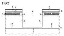
図2は、絶縁層2に至るまで半導体材料をエッチングした後の、さらなる中間生成物の断面図である。このエッチング工程は、RIE(リアクティブ・イオン・エッチング)によって、好ましくはDRIE(ディープ・リアクティブ・イオン・エッチング)によって行われる。この場合、絶縁層2はエッチング停止層として機能する。 FIG. 2 is a cross-sectional view of a further intermediate product after etching the semiconductor material down to the insulating
開口部9は、このように図2の断面図に対応するように絶縁層2に到達するまで形成される。エッチングは基板の上面と直角に、つまり、大きく異方的に施すことができ、それによって、開口部9の側壁をできるだけ急斜面にし、開口部9の横への広がりをビアコンタクトのために必要な直径を超えないようにすることができる。 The
図3は、誘電体層10が成膜された後の、さらなる中間生成物を示す、図2に準ずる断面図である。誘電体層10がまず表面全体に成膜される。誘電体層10は、例えば、半導体材料の酸化物、特に二酸化ケイ素であってよい。誘電体層10を成膜するには、CVD法(化学蒸着)、特に、SACVD(準常圧化学蒸着)法を用いるのが適切である。この方法は、それ自体が半導体技術の分野で周知である。 FIG. 3 is a cross-sectional view according to FIG. 2 showing a further intermediate product after the
次いで、図4の断面図に示すように、誘電体層10は、その上面部分、つまりライナ6と、そして開口部9の底部との部分が除去される。その結果、この時点で誘電体層10は開口部9の側壁上にのみ存在することになる。 Next, as shown in the cross-sectional view of FIG. 4, the top surface portion of the
図3及び4は、絶縁層2及び誘電体層10が共に酸化物から成っていてもよいことを示すため、これら2つの層の間の境界線を省略している。誘電体層10を部分的に除去することは、例えばRIEによって可能である。このため、誘電体層10は、特に、CMOS回路が位置する素子部分の上面から除去される。 3 and 4 omit the boundary line between these two layers to show that both the insulating
ライナ6、特にTi/TiNからなるライナはここではエッチング停止層として使用される。同様に、半導体材料の酸化物が金属間誘電体4として使用されると都合がよい。異方性エッチングを行うことによって、水平面上の誘電体層10は完全に除去される一方、開口部の側壁上の誘電体層10は、絶縁に必要なだけの厚みを有する状態で残る。接続パッド7もエッチング停止層として使用される。 The
図5は、誘電体層10の成膜と同様に、金属膜11をまずは表面全体に成膜した後の、図4に準ずる別の断面図である。金属膜11は、例えば等方的なMOCVD(有機金属化学気相成長)法によって形成可能であり、例えばタングステンよりなる。 FIG. 5 is another cross-sectional view similar to FIG. 4 after the
最初に表面全体を覆っている金属膜11は、マスクを使わずにエッチバックすることができる。このエッチバックは、上面でのエッチング率が開口部9の底部及び側壁におけるエッチング率よりも高くなるように行われる。 The
このように、CMOS回路の領域に金属膜11を完全に除去しても、金属を開口部9の底部及び側壁に十分残すことができる。Thus, even if the
図6は、金属膜が部分的にエッチバックされた後の、図5に準ずる断面図であり、この時点では金属膜が開口部9の底部及び側壁に部分的に残っているだけである。接続パッド7は開口部9の底部において誘電体層10から露出しているので、金属膜11と接続パッド7との間は電気的に接続される。 FIG. 6 is a cross-sectional view according to FIG. 5 after the metal film is partially etched back, at which point the metal film is only partially left on the bottom and side walls of the
下記記載において頂部金属と呼ばれる上縁接続金属膜を成膜することにより、金属膜11はその上縁が上縁接続金属膜に接触する。よって、金属膜11には、導電路に通常使用される金属、例えばアルミニウムが適切である。 By forming an upper edge connection metal film called a top metal in the following description, the upper edge of the
図7は、開口部9の縁を構成する上縁の上に、内縁部を有する頂部金属12の層が成膜された後の、図6に準ずる断面図である。前記内縁部は図7に示すものより大きくても小さくてもよい。 FIG. 7 is a cross-sectional view according to FIG. 6 after a layer of the
このようにして、金属膜11の残留部分と頂部金属12との間の導電性接続部が確実に形成される。すなわち、頂部金属12を成膜することによって、そのまま金属膜11と頂部金属12とは電気的に接続されることになる。ここで、頂部金属12は、所定の接続部として構成される。 In this way, a conductive connection between the remaining portion of the
素子の上面は開口部9があるために平面ではないので、縁部分にも十分に均一なマスク層を形成するために、吹き付け塗装、特にナノスプレーとして知られる方法によって形成されるレジストマスクを使用することが好ましい。厚さの十分なレジストを成膜することにより、結果的に適切なマスク層の形成が可能となる。 Since the top surface of the device is not flat because of the
図8は、保護膜13を全面に成膜した後の、図7に準ずる断面図である。保護膜13は図示された実施形態においてはかなり薄く、開口部9を埋め尽くしてはいない。保護膜13は単層あるいは複層であって、例えば、酸化物層(特に酸化ケイ素層)とその上の窒化物層(特に窒化ケイ素層)とによって形成することができる。保護膜13は、標準PECVD(プラズマCVD)法あるいはSACVD(準常圧CVD)法によって成膜してもよい。複層保護膜13は一部分をPECVD法、また別の部分をSACVD法によって成膜することも可能である。また、保護膜13はレジストマスクを用いて形成することもできる。 FIG. 8 is a cross-sectional view similar to FIG. 7 after the
複層保護膜13を含む実施形態に関しては、全工程の進行において、焼き戻し処理を行う際に重要な当該材料の特性、例えば熱膨張係数、が考慮されなければならない。そうしないと、主に開口部9の側壁部分の金属膜11を覆う部分において、保護膜13がひび割れたり、あるいは下地から剥離したりしてしまう。このような事態は、例えば、集積部品構成部の領域にあるシリコンのいわゆる未結合手(ダングリングボンド、dangling bond)を飽和させるため、形成ガス発生雰囲気の下で(例えば、水素及び窒素の混合ガスの下で)素子を通常400℃から500℃まで加熱する焼き戻し処理(形成ガス処理(forming gas alloy)と呼ばれている)が行われる際に、回避することが必須である。 With respect to the embodiment including the multilayer
このような実施形態に関しては、保護膜を成膜する前に、あるいは、少なくとも、保護膜13の層の上に異なる材料からなる別の層を成膜する前には、焼き戻し処理を既に終えていることが好ましい。つまり上述の例では、酸化物層の上に窒化物層を成膜する前に、あるいは、別の層を異なる方法によって(例えば、PECVD法の代わりにSACVD法を用いて)成膜する前に、焼き戻し処理を既に終えていることが好ましい。
これらの成膜の、従って、異なる熱特性の層を有する実施形態においては、焼き戻し処理は保護膜13を成膜する前、あるいは完全に成膜し終える前に行われるのが好ましい。よって、いずれの場合も、焼き戻し処理は、保護膜13の最後の層が形成される前に行われる。With respect to such an embodiment, the tempering process has already been completed before forming the protective film, or at least before forming another layer made of a different material on the layer of the
In these film formations, and therefore in embodiments having different thermal properties, the tempering treatment is preferably performed before or after the
図8の断面図に示した構造に続いて、接続パッド7の領域にその裏面から凹部を形成し、よって接続パッド7の裏面を露出させるという簡単な方法でビアコンタクトを完成させることができる。この場合、頂部金属12と基板1の裏面との間に連続してこれらを導電接続する、さらなる金属膜を成膜することができる。従来技術がビアコンタクトの表面および裏面の両方の金属接触の形成にマスクを必要とすることを鑑みれば、上記方法は従来技術よりも格段に容易である。 Following the structure shown in the cross-sectional view of FIG. 8, a via contact can be completed by a simple method in which a recess is formed in the region of the connection pad 7 from the back surface thereof, thereby exposing the back surface of the connection pad 7. In this case, a further metal film can be formed between the
標準CMOSプロセスと比較すると、上記方法では、開口部9を形成するためのエッチング工程を除けば、マスクを追加する必要がない。従って、特に基板を貫通するビアコンタクトを備えたCMOS部品を製造する場合には当該方法が適している。本発明の部品の構造は、内蔵された接続パッド7によって特徴づけられるだけではなく、開口部9の内部全体に充填される代わりに、その側壁においてのみ存在するビアコンタクトの導電接続によっても特徴づけられる。この構造は、上記目的のために使用される開口部の側壁が比較的非常に大きな表面積を有するためにビアコンタクトのオーム抵抗が殊に低く、また、保護膜13を標準PECVDプロセス及び随意的にSACVDプロセスによって成膜できる、という特有の効果を発揮する。 Compared with a standard CMOS process, in the above method, it is not necessary to add a mask except for an etching process for forming the
1 基板
2 絶縁層
3 半導体層
4 金属間誘電体
5 金属層
6 ライナ
7 接続パッド
8 マスク
9 開口部
10 誘電体層
11 金属膜
12 頂部金属
13 保護膜DESCRIPTION OF
Claims (17)
Translated fromJapanese前記接続パッド(7)の上部に、基板(1)の上面から絶縁層(2)に至る開口部(9)を形成し、
誘電体層(10)を成膜し、
誘電体層(10)及び絶縁層(2)を、接続パッド(7)の上面が露出する程度に、開口部(9)内から除去し、
接続パッド(7)と接触する金属膜(11)を成膜し、
そして、
ビアコンタクトを、開口部(9)の反対に位置する側の基板(1)の裏面から接続パッド(7)に至るまで形成することを特徴とする、半導体素子の製造方法。Forming a built-in insulating layer (2) and a connecting pad (7) made of a conductive material disposed on the insulating layer (2) on a substrate (1) made of a semiconductor material;
An opening (9) from the upper surface of the substrate (1) to the insulating layer (2) is formed on the connection pad (7),
Forming a dielectric layer (10);
The dielectric layer (10) and the insulating layer (2) are removed from the opening (9) to such an extent that the upper surface of the connection pad (7) is exposed,
Forming a metal film (11) in contact with the connection pad (7);
And
A method for manufacturing a semiconductor device, characterized in that a via contact is formed from the back surface of the substrate (1) on the side opposite to the opening (9) to the connection pad (7).
頂部金属(12)を、金属膜(11)の上縁に接触するように成膜することを特徴とする、請求項1あるいは2に記載の方法。While removing the metal film (11) outside the opening (9),
The method according to claim 1 or 2, characterized in that the top metal (12) is deposited in contact with the upper edge of the metal film (11).
金属間誘電体(4)の上面は、ライナ6で覆われ、
ライナ(6)が誘電体層(10)の部分除去のためのエッチング停止層として機能するようにライナ6の材料が選択されることを特徴とする、請求項1から4のいずれかに記載の方法。The upper surface of the substrate (1) is provided with an intermetallic dielectric (4) and a metal layer (5) of wiring before the opening (9) is formed by etching,
The top surface of the intermetal dielectric (4) is covered with a liner 6;
5. The liner 6 according to claim 1, wherein the liner 6 is selected such that the liner 6 functions as an etch stop layer for partial removal of the dielectric layer 10. Method.
第2半導体本体を前記絶縁層(2)上に載置し、
前記半導体本体の接続に先立ち、接続パッド(7)を、前記絶縁層(2)の上あるいは、前記絶縁層(2)に接続される第2半導体本体の上部に成膜することを特徴とする、請求項1から5のいずれかに記載の方法。Producing a substrate (1) such that the first semiconductor body comprises an insulator layer (2) on its upper surface;
Placing a second semiconductor body on the insulating layer (2);
Prior to connection of the semiconductor body, a connection pad (7) is formed on the insulating layer (2) or on the second semiconductor body connected to the insulating layer (2). The method according to claim 1.
前記接続パッド(7)に導電接続されるともに、前記基板に形成された開口部(9)の側壁を覆う金属膜(11)が設けられ、
接続パッド(7)まで延びるビアコンタクトが、開口部(9)の反対に位置する側の基板(1)の裏面に設けられていることを特徴とする、ビアコンタクトを備えた半導体素子。A substrate (1) comprising a built-in insulating layer (2) and a conductive connection pad (7) disposed on the insulating layer (2);
A metal film (11) that is conductively connected to the connection pad (7) and covers a side wall of the opening (9) formed in the substrate is provided.
A semiconductor element provided with a via contact, characterized in that a via contact extending to the connection pad (7) is provided on the back surface of the substrate (1) on the side opposite to the opening (9).
Applications Claiming Priority (3)
| Application Number | Priority Date | Filing Date | Title |
|---|---|---|---|
| DE102008033395ADE102008033395B3 (en) | 2008-07-16 | 2008-07-16 | Method for producing a semiconductor component and semiconductor component |
| DE102008033395.6 | 2008-07-16 | ||
| PCT/EP2009/058001WO2010006916A1 (en) | 2008-07-16 | 2009-06-25 | Method for producing a semiconductor component, and semiconductor component |
Publications (2)
| Publication Number | Publication Date |
|---|---|
| JP2011527512Atrue JP2011527512A (en) | 2011-10-27 |
| JP5497756B2 JP5497756B2 (en) | 2014-05-21 |
Family
ID=41051152
Family Applications (1)
| Application Number | Title | Priority Date | Filing Date |
|---|---|---|---|
| JP2011517083AActiveJP5497756B2 (en) | 2008-07-16 | 2009-06-25 | Semiconductor device manufacturing method and semiconductor device |
Country Status (4)
| Country | Link |
|---|---|
| US (1) | US8658534B2 (en) |
| JP (1) | JP5497756B2 (en) |
| DE (1) | DE102008033395B3 (en) |
| WO (1) | WO2010006916A1 (en) |
Families Citing this family (20)
| Publication number | Priority date | Publication date | Assignee | Title |
|---|---|---|---|---|
| DE102009004725A1 (en) | 2009-01-15 | 2010-07-29 | Austriamicrosystems Ag | Through-hole semiconductor circuit and method of manufacturing vertically integrated circuits |
| DE102009049102B4 (en) | 2009-10-13 | 2012-10-04 | Austriamicrosystems Ag | Semiconductor device with via and method for producing a via in a semiconductor device |
| TWI546925B (en)* | 2010-02-09 | 2016-08-21 | 精材科技股份有限公司 | Package and method for forming the same |
| JP6342033B2 (en)* | 2010-06-30 | 2018-06-13 | キヤノン株式会社 | Solid-state imaging device |
| JP2012033894A (en) | 2010-06-30 | 2012-02-16 | Canon Inc | Solid state image sensor |
| US8697569B2 (en) | 2010-07-23 | 2014-04-15 | Tessera, Inc. | Non-lithographic formation of three-dimensional conductive elements |
| DE102010045055B4 (en) | 2010-09-10 | 2019-03-28 | Austriamicrosystems Ag | Method for producing a semiconductor component with a plated through hole |
| US8847233B2 (en)* | 2011-05-12 | 2014-09-30 | Semiconductor Energy Laboratory Co., Ltd. | Semiconductor device having a trenched insulating layer coated with an oxide semiconductor film |
| DE102011104305A1 (en)* | 2011-06-16 | 2012-12-20 | Austriamicrosystems Ag | Production method for a semiconductor component with a conductor layer in the semiconductor body and semiconductor component |
| DE102011080774B4 (en)* | 2011-08-10 | 2015-02-19 | Hahn-Schickard-Gesellschaft für angewandte Forschung e.V. | METHOD FOR PRODUCING A SEMICONDUCTOR STRUCTURE AND SEMICONDUCTOR STRUCTURE |
| EP2693467B1 (en) | 2012-08-01 | 2015-11-18 | ams AG | A method of producing a semiconductor device having an interconnect through the substrate |
| EP2741322B1 (en) | 2012-12-10 | 2016-04-27 | ams AG | Semiconductor device with integrated hot plate and recessed substrate and method of production |
| EP2772939B1 (en) | 2013-03-01 | 2016-10-19 | Ams Ag | Semiconductor device for detection of radiation and method of producing a semiconductor device for detection of radiation |
| EP3604207A1 (en) | 2013-03-05 | 2020-02-05 | Ams Ag | Semiconductor device with capacitive sensor and integrated circuit |
| EP2775275B1 (en) | 2013-03-08 | 2015-12-16 | Ams Ag | Ultraviolet semiconductor sensor device and method of measuring ultraviolet radiation |
| EP2790211B1 (en) | 2013-04-10 | 2018-06-20 | Ams Ag | Method of producing a through-substrate via in a semiconductor device and semiconductor device comprising a through-substrate via |
| EP2899760B1 (en) | 2014-01-27 | 2018-08-29 | ams AG | Semiconductor device for optical applications and method of producing such a semiconductor device |
| EP3312874A1 (en) | 2016-10-20 | 2018-04-25 | ams AG | Method of forming a through-substrate via and a semiconductor device comprising a through-substrate via |
| EP3550600B1 (en) | 2018-04-04 | 2020-08-05 | ams AG | Method of forming a through-substrate via and semiconductor device comprising the through-substrate via |
| WO2019226432A1 (en)* | 2018-05-21 | 2019-11-28 | Corning Incorporated | Liquid lenses and methods of manufacturing liquid lenses |
Citations (13)
| Publication number | Priority date | Publication date | Assignee | Title |
|---|---|---|---|---|
| JPH01128562A (en)* | 1987-11-13 | 1989-05-22 | Nissan Motor Co Ltd | semiconductor equipment |
| JPH04304663A (en)* | 1991-04-02 | 1992-10-28 | Nissan Motor Co Ltd | semiconductor device |
| JPH07505982A (en)* | 1993-01-19 | 1995-06-29 | ヒューズ・エアクラフト・カンパニー | Method for forming deep conductive feedthroughs and wiring layer including feedthroughs formed according to the method |
| JP2002508590A (en)* | 1998-03-26 | 2002-03-19 | フラウンホッファー−ゲゼルシャフト ツァ フェルダールング デァ アンゲヴァンテン フォアシュンク エー.ファオ. | Wiring method for manufacturing vertically integrated circuit structure and vertically integrated circuit structure |
| JP2004349513A (en)* | 2003-05-22 | 2004-12-09 | Seiko Epson Corp | Thin film circuit device and method for manufacturing the same, electro-optical device, and electronic equipment |
| JP2005012180A (en)* | 2003-05-28 | 2005-01-13 | Okutekku:Kk | Semiconductor device and manufacturing method thereof |
| JP2005116623A (en)* | 2003-10-03 | 2005-04-28 | Nec Electronics Corp | Semiconductor device and manufacturing method thereof |
| JP2006128172A (en)* | 2004-10-26 | 2006-05-18 | Sanyo Electric Co Ltd | Semiconductor apparatus and its manufacturing method |
| WO2006131209A2 (en)* | 2005-06-07 | 2006-12-14 | Austriamicrosystems Ag | Photodiode with integrated semiconductor circuit and method for the production thereof |
| JP2007242676A (en)* | 2006-03-06 | 2007-09-20 | Sanyo Electric Co Ltd | Semiconductor device manufacturing method |
| JP2007305960A (en)* | 2006-04-14 | 2007-11-22 | Sharp Corp | Semiconductor device and manufacturing method thereof |
| JP2008085020A (en)* | 2006-09-27 | 2008-04-10 | Nec Electronics Corp | Semiconductor device |
| US20080157394A1 (en)* | 2006-12-29 | 2008-07-03 | Samsung Electronics Co., Ltd. | Semiconductor packages, stacked semiconductor packages, and methods of manufacturing the semiconductor packages and the stacked semiconductor packages |
Family Cites Families (22)
| Publication number | Priority date | Publication date | Assignee | Title |
|---|---|---|---|---|
| US3986196A (en) | 1975-06-30 | 1976-10-12 | Varian Associates | Through-substrate source contact for microwave FET |
| DE3850855T2 (en)* | 1987-11-13 | 1994-11-10 | Nissan Motor | Semiconductor device. |
| US5426072A (en)* | 1993-01-21 | 1995-06-20 | Hughes Aircraft Company | Process of manufacturing a three dimensional integrated circuit from stacked SOI wafers using a temporary silicon substrate |
| DE4400985C1 (en) | 1994-01-14 | 1995-05-11 | Siemens Ag | Method for producing a three-dimensional circuit arrangement |
| US5511428A (en) | 1994-06-10 | 1996-04-30 | Massachusetts Institute Of Technology | Backside contact of sensor microstructures |
| DE4433846C2 (en) | 1994-09-22 | 1999-06-02 | Fraunhofer Ges Forschung | Method of making a vertical integrated circuit structure |
| JP3177436B2 (en) | 1996-03-21 | 2001-06-18 | 株式会社日立製作所 | Semiconductor integrated circuit device |
| JP3056689B2 (en) | 1996-07-09 | 2000-06-26 | 松下電器産業株式会社 | Semiconductor device and manufacturing method thereof |
| EP0926723B1 (en) | 1997-11-26 | 2007-01-17 | STMicroelectronics S.r.l. | Process for forming front-back through contacts in micro-integrated electronic devices |
| TW442873B (en) | 1999-01-14 | 2001-06-23 | United Microelectronics Corp | Three-dimension stack-type chip structure and its manufacturing method |
| DE19904571C1 (en)* | 1999-02-04 | 2000-04-20 | Siemens Ag | Three-dimensional IC, e.g. a DRAM cell array, is produced by electron beam passage through a substrate to locate an alignment structure in a bonded second substrate for mask alignment |
| US6352923B1 (en) | 1999-03-01 | 2002-03-05 | United Microelectronics Corp. | Method of fabricating direct contact through hole type |
| US6159833A (en) | 1999-09-08 | 2000-12-12 | United Microelectronics Corp. | Method of forming a contact hole in a semiconductor wafer |
| JP2001116768A (en) | 1999-10-20 | 2001-04-27 | Shin Etsu Polymer Co Ltd | Semiconductor wafer and contact for semiconductor chip |
| US6483147B1 (en) | 1999-10-25 | 2002-11-19 | Advanced Micro Devices, Inc. | Through wafer backside contact to improve SOI heat dissipation |
| US6818464B2 (en) | 2001-10-17 | 2004-11-16 | Hymite A/S | Double-sided etching technique for providing a semiconductor structure with through-holes, and a feed-through metalization process for sealing the through-holes |
| DE10200399B4 (en) | 2002-01-08 | 2008-03-27 | Advanced Micro Devices, Inc., Sunnyvale | A method for producing a three-dimensionally integrated semiconductor device and a three-dimensionally integrated semiconductor device |
| US6930040B2 (en) | 2003-10-22 | 2005-08-16 | Taiwan Semiconductor Manufacturing Company, Ltd. | Method of forming a contact on a silicon-on-insulator wafer |
| DE10351201B3 (en)* | 2003-11-03 | 2005-07-14 | Infineon Technologies Ag | Neuro-sensor and process to manufacture a semiconductor neuro-sensor on a transistorized foundation structure |
| US20050156330A1 (en) | 2004-01-21 | 2005-07-21 | Harris James M. | Through-wafer contact to bonding pad |
| US7553695B2 (en)* | 2005-03-17 | 2009-06-30 | Hymite A/S | Method of fabricating a package for a micro component |
| US7923840B2 (en) | 2007-01-10 | 2011-04-12 | International Business Machines Corporation | Electrically conductive path forming below barrier oxide layer and integrated circuit |
- 2008
- 2008-07-16DEDE102008033395Apatent/DE102008033395B3/enactiveActive
- 2009
- 2009-06-25USUS13/054,614patent/US8658534B2/enactiveActive
- 2009-06-25JPJP2011517083Apatent/JP5497756B2/enactiveActive
- 2009-06-25WOPCT/EP2009/058001patent/WO2010006916A1/enactiveApplication Filing
Patent Citations (13)
| Publication number | Priority date | Publication date | Assignee | Title |
|---|---|---|---|---|
| JPH01128562A (en)* | 1987-11-13 | 1989-05-22 | Nissan Motor Co Ltd | semiconductor equipment |
| JPH04304663A (en)* | 1991-04-02 | 1992-10-28 | Nissan Motor Co Ltd | semiconductor device |
| JPH07505982A (en)* | 1993-01-19 | 1995-06-29 | ヒューズ・エアクラフト・カンパニー | Method for forming deep conductive feedthroughs and wiring layer including feedthroughs formed according to the method |
| JP2002508590A (en)* | 1998-03-26 | 2002-03-19 | フラウンホッファー−ゲゼルシャフト ツァ フェルダールング デァ アンゲヴァンテン フォアシュンク エー.ファオ. | Wiring method for manufacturing vertically integrated circuit structure and vertically integrated circuit structure |
| JP2004349513A (en)* | 2003-05-22 | 2004-12-09 | Seiko Epson Corp | Thin film circuit device and method for manufacturing the same, electro-optical device, and electronic equipment |
| JP2005012180A (en)* | 2003-05-28 | 2005-01-13 | Okutekku:Kk | Semiconductor device and manufacturing method thereof |
| JP2005116623A (en)* | 2003-10-03 | 2005-04-28 | Nec Electronics Corp | Semiconductor device and manufacturing method thereof |
| JP2006128172A (en)* | 2004-10-26 | 2006-05-18 | Sanyo Electric Co Ltd | Semiconductor apparatus and its manufacturing method |
| WO2006131209A2 (en)* | 2005-06-07 | 2006-12-14 | Austriamicrosystems Ag | Photodiode with integrated semiconductor circuit and method for the production thereof |
| JP2007242676A (en)* | 2006-03-06 | 2007-09-20 | Sanyo Electric Co Ltd | Semiconductor device manufacturing method |
| JP2007305960A (en)* | 2006-04-14 | 2007-11-22 | Sharp Corp | Semiconductor device and manufacturing method thereof |
| JP2008085020A (en)* | 2006-09-27 | 2008-04-10 | Nec Electronics Corp | Semiconductor device |
| US20080157394A1 (en)* | 2006-12-29 | 2008-07-03 | Samsung Electronics Co., Ltd. | Semiconductor packages, stacked semiconductor packages, and methods of manufacturing the semiconductor packages and the stacked semiconductor packages |
Also Published As
| Publication number | Publication date |
|---|---|
| WO2010006916A1 (en) | 2010-01-21 |
| US8658534B2 (en) | 2014-02-25 |
| DE102008033395B3 (en) | 2010-02-04 |
| US20110260284A1 (en) | 2011-10-27 |
| JP5497756B2 (en) | 2014-05-21 |
Similar Documents
| Publication | Publication Date | Title |
|---|---|---|
| JP5497756B2 (en) | Semiconductor device manufacturing method and semiconductor device | |
| US8421238B2 (en) | Stacked semiconductor device with through via | |
| CN101197298B (en) | Method for manufacturing semiconductor device and semiconductor device | |
| CN101783329B (en) | Semiconductor element and its manufacturing method | |
| US7902069B2 (en) | Small area, robust silicon via structure and process | |
| JP5201048B2 (en) | Semiconductor device and manufacturing method thereof | |
| US8742590B2 (en) | Method for forming isolation trenches | |
| TWI525776B (en) | Optimized ring-shaped copper through-substrate perforation | |
| US8592310B2 (en) | Methods of manufacturing a semiconductor device | |
| CN108140559A (en) | Conductive barrier direct hybrid bonding | |
| US9355895B2 (en) | Method of providing a via hole and routing structure | |
| TW201222773A (en) | Integrated circuit device and method of forming the same | |
| US8704358B2 (en) | Method for forming an integrated circuit | |
| JP2010080750A (en) | Semiconductor device, and method of manufacturing the same | |
| CN103489840B (en) | Through-silicon via and manufacturing method thereof | |
| TWI705527B (en) | Method of forming integrated circuit structure, integrated circuit device, and integrated circuit structure | |
| US20120032339A1 (en) | Integrated circuit structure with through via for heat evacuating | |
| JP5377657B2 (en) | Manufacturing method of semiconductor device | |
| CN102760710A (en) | Through silicon via structure and forming method thereof | |
| CN109712953B (en) | Manufacturing method of semiconductor device and semiconductor device | |
| EP2584598B1 (en) | Method of producing a semiconductor device comprising a through-substrate via and a capping layer and corresponding semiconductor device | |
| CN105097645B (en) | Method for manufacturing semiconductor device | |
| CN116013848A (en) | Method for forming through silicon via, method for forming semiconductor element, and semiconductor element | |
| TW201250970A (en) | Method for fabricating through-silicon via structure |
Legal Events
| Date | Code | Title | Description |
|---|---|---|---|
| A977 | Report on retrieval | Free format text:JAPANESE INTERMEDIATE CODE: A971007 Effective date:20130214 | |
| A131 | Notification of reasons for refusal | Free format text:JAPANESE INTERMEDIATE CODE: A131 Effective date:20130220 | |
| A521 | Request for written amendment filed | Free format text:JAPANESE INTERMEDIATE CODE: A523 Effective date:20130515 | |
| A131 | Notification of reasons for refusal | Free format text:JAPANESE INTERMEDIATE CODE: A131 Effective date:20131009 | |
| A521 | Request for written amendment filed | Free format text:JAPANESE INTERMEDIATE CODE: A523 Effective date:20140107 | |
| TRDD | Decision of grant or rejection written | ||
| A01 | Written decision to grant a patent or to grant a registration (utility model) | Free format text:JAPANESE INTERMEDIATE CODE: A01 Effective date:20140205 | |
| A61 | First payment of annual fees (during grant procedure) | Free format text:JAPANESE INTERMEDIATE CODE: A61 Effective date:20140306 | |
| R150 | Certificate of patent or registration of utility model | Ref document number:5497756 Country of ref document:JP Free format text:JAPANESE INTERMEDIATE CODE: R150 | |
| R250 | Receipt of annual fees | Free format text:JAPANESE INTERMEDIATE CODE: R250 | |
| R250 | Receipt of annual fees | Free format text:JAPANESE INTERMEDIATE CODE: R250 | |
| R250 | Receipt of annual fees | Free format text:JAPANESE INTERMEDIATE CODE: R250 | |
| R250 | Receipt of annual fees | Free format text:JAPANESE INTERMEDIATE CODE: R250 | |
| R250 | Receipt of annual fees | Free format text:JAPANESE INTERMEDIATE CODE: R250 | |
| R250 | Receipt of annual fees | Free format text:JAPANESE INTERMEDIATE CODE: R250 | |
| R250 | Receipt of annual fees | Free format text:JAPANESE INTERMEDIATE CODE: R250 | |
| R250 | Receipt of annual fees | Free format text:JAPANESE INTERMEDIATE CODE: R250 |