JP2011508373A - Discrete light emitting element and planar assembly thereof - Google Patents
Discrete light emitting element and planar assembly thereofDownload PDFInfo
- Publication number
- JP2011508373A JP2011508373AJP2010539043AJP2010539043AJP2011508373AJP 2011508373 AJP2011508373 AJP 2011508373AJP 2010539043 AJP2010539043 AJP 2010539043AJP 2010539043 AJP2010539043 AJP 2010539043AJP 2011508373 AJP2011508373 AJP 2011508373A
- Authority
- JP
- Japan
- Prior art keywords
- light
- light guide
- region
- guide element
- coupling region
- Prior art date
- Legal status (The legal status is an assumption and is not a legal conclusion. Google has not performed a legal analysis and makes no representation as to the accuracy of the status listed.)
- Withdrawn
Links
- 230000008878couplingEffects0.000claimsabstractdescription373
- 238000010168coupling processMethods0.000claimsabstractdescription373
- 238000005859coupling reactionMethods0.000claimsabstractdescription373
- 238000005286illuminationMethods0.000claimsabstractdescription158
- 230000010354integrationEffects0.000claimsabstractdescription51
- 230000004927fusionEffects0.000claimsabstractdescription5
- 238000000034methodMethods0.000claimsdescription71
- 239000000463materialSubstances0.000claimsdescription47
- 230000000717retained effectEffects0.000claimsdescription19
- 238000000149argon plasma sinteringMethods0.000claimsdescription14
- 230000005855radiationEffects0.000claimsdescription11
- 230000008859changeEffects0.000claimsdescription7
- 239000008393encapsulating agentSubstances0.000claimsdescription5
- 238000005452bendingMethods0.000claimsdescription4
- 239000011248coating agentSubstances0.000claimsdescription3
- 238000000576coating methodMethods0.000claimsdescription3
- 230000000295complement effectEffects0.000claimsdescription3
- 230000007423decreaseEffects0.000claimsdescription3
- 238000005304joiningMethods0.000claimsdescription3
- 239000004973liquid crystal related substanceSubstances0.000claimsdescription3
- 238000009827uniform distributionMethods0.000claimsdescription3
- 239000011358absorbing materialSubstances0.000claimsdescription2
- 239000011159matrix materialSubstances0.000claimsdescription2
- 239000002245particleSubstances0.000description23
- 230000007704transitionEffects0.000description20
- 230000003287optical effectEffects0.000description15
- 238000009792diffusion processMethods0.000description8
- 238000009826distributionMethods0.000description8
- 239000000945fillerSubstances0.000description8
- 239000002775capsuleSubstances0.000description5
- 238000010586diagramMethods0.000description5
- 230000008901benefitEffects0.000description3
- 230000014509gene expressionEffects0.000description3
- 230000017525heat dissipationEffects0.000description3
- 230000001902propagating effectEffects0.000description3
- 238000005476solderingMethods0.000description3
- 238000009825accumulationMethods0.000description2
- 239000000853adhesiveSubstances0.000description2
- 230000001070adhesive effectEffects0.000description2
- 239000011324beadSubstances0.000description2
- 230000005540biological transmissionEffects0.000description2
- 239000011247coating layerSubstances0.000description2
- 239000012792core layerSubstances0.000description2
- 238000004519manufacturing processMethods0.000description2
- 229920003229poly(methyl methacrylate)Polymers0.000description2
- 239000004417polycarbonateSubstances0.000description2
- 229920000515polycarbonatePolymers0.000description2
- 229920000642polymerPolymers0.000description2
- 239000004926polymethyl methacrylateSubstances0.000description2
- 239000007787solidSubstances0.000description2
- VVQNEPGJFQJSBK-UHFFFAOYSA-NMethyl methacrylateChemical compoundCOC(=O)C(C)=CVVQNEPGJFQJSBK-UHFFFAOYSA-N0.000description1
- 239000004677NylonSubstances0.000description1
- 239000002033PVDF binderSubstances0.000description1
- VYPSYNLAJGMNEJ-UHFFFAOYSA-NSilicium dioxideChemical compoundO=[Si]=OVYPSYNLAJGMNEJ-UHFFFAOYSA-N0.000description1
- 229910010413TiO 2Inorganic materials0.000description1
- 230000004931aggregating effectEffects0.000description1
- 125000001931aliphatic groupChemical group0.000description1
- 125000003118aryl groupChemical group0.000description1
- -1but not limited toSubstances0.000description1
- 239000000919ceramicSubstances0.000description1
- 239000002131composite materialSubstances0.000description1
- 239000006185dispersionSubstances0.000description1
- 230000000694effectsEffects0.000description1
- 238000005516engineering processMethods0.000description1
- 239000000835fiberSubstances0.000description1
- 239000011888foilSubstances0.000description1
- 239000000499gelSubstances0.000description1
- 239000011521glassSubstances0.000description1
- 238000001746injection mouldingMethods0.000description1
- 229910010272inorganic materialInorganic materials0.000description1
- 239000011147inorganic materialSubstances0.000description1
- 239000010410layerSubstances0.000description1
- 239000002502liposomeSubstances0.000description1
- 238000012423maintenanceMethods0.000description1
- 230000014759maintenance of locationEffects0.000description1
- 238000002844meltingMethods0.000description1
- 230000008018meltingEffects0.000description1
- 229920001778nylonPolymers0.000description1
- 238000005498polishingMethods0.000description1
- 229920002981polyvinylidene fluoridePolymers0.000description1
- 230000008569processEffects0.000description1
- 230000000644propagated effectEffects0.000description1
- 239000011347resinSubstances0.000description1
- 229920005989resinPolymers0.000description1
- 229910052710siliconInorganic materials0.000description1
- 239000010703siliconSubstances0.000description1
- 230000000087stabilizing effectEffects0.000description1
- 238000006467substitution reactionMethods0.000description1
- 229920001169thermoplasticPolymers0.000description1
- 239000004416thermosoftening plasticSubstances0.000description1
Images


Classifications
- G—PHYSICS
- G02—OPTICS
- G02B—OPTICAL ELEMENTS, SYSTEMS OR APPARATUS
- G02B6/00—Light guides; Structural details of arrangements comprising light guides and other optical elements, e.g. couplings
- G02B6/0001—Light guides; Structural details of arrangements comprising light guides and other optical elements, e.g. couplings specially adapted for lighting devices or systems
- G02B6/0011—Light guides; Structural details of arrangements comprising light guides and other optical elements, e.g. couplings specially adapted for lighting devices or systems the light guides being planar or of plate-like form
- G02B6/0065—Manufacturing aspects; Material aspects
- G—PHYSICS
- G02—OPTICS
- G02B—OPTICAL ELEMENTS, SYSTEMS OR APPARATUS
- G02B6/00—Light guides; Structural details of arrangements comprising light guides and other optical elements, e.g. couplings
- G02B6/0001—Light guides; Structural details of arrangements comprising light guides and other optical elements, e.g. couplings specially adapted for lighting devices or systems
- G02B6/0011—Light guides; Structural details of arrangements comprising light guides and other optical elements, e.g. couplings specially adapted for lighting devices or systems the light guides being planar or of plate-like form
- G02B6/0075—Arrangements of multiple light guides
- G02B6/0078—Side-by-side arrangements, e.g. for large area displays
- G02B6/008—Side-by-side arrangements, e.g. for large area displays of the partially overlapping type
- G—PHYSICS
- G02—OPTICS
- G02B—OPTICAL ELEMENTS, SYSTEMS OR APPARATUS
- G02B6/00—Light guides; Structural details of arrangements comprising light guides and other optical elements, e.g. couplings
- G02B6/0001—Light guides; Structural details of arrangements comprising light guides and other optical elements, e.g. couplings specially adapted for lighting devices or systems
- G02B6/0011—Light guides; Structural details of arrangements comprising light guides and other optical elements, e.g. couplings specially adapted for lighting devices or systems the light guides being planar or of plate-like form
- G02B6/0066—Light guides; Structural details of arrangements comprising light guides and other optical elements, e.g. couplings specially adapted for lighting devices or systems the light guides being planar or of plate-like form characterised by the light source being coupled to the light guide
- G02B6/0068—Arrangements of plural sources, e.g. multi-colour light sources
- G—PHYSICS
- G02—OPTICS
- G02B—OPTICAL ELEMENTS, SYSTEMS OR APPARATUS
- G02B6/00—Light guides; Structural details of arrangements comprising light guides and other optical elements, e.g. couplings
- G02B6/0001—Light guides; Structural details of arrangements comprising light guides and other optical elements, e.g. couplings specially adapted for lighting devices or systems
- G02B6/0011—Light guides; Structural details of arrangements comprising light guides and other optical elements, e.g. couplings specially adapted for lighting devices or systems the light guides being planar or of plate-like form
- G02B6/0066—Light guides; Structural details of arrangements comprising light guides and other optical elements, e.g. couplings specially adapted for lighting devices or systems the light guides being planar or of plate-like form characterised by the light source being coupled to the light guide
- G02B6/0073—Light emitting diode [LED]
- G—PHYSICS
- G02—OPTICS
- G02B—OPTICAL ELEMENTS, SYSTEMS OR APPARATUS
- G02B6/00—Light guides; Structural details of arrangements comprising light guides and other optical elements, e.g. couplings
- G02B6/0001—Light guides; Structural details of arrangements comprising light guides and other optical elements, e.g. couplings specially adapted for lighting devices or systems
- G02B6/0011—Light guides; Structural details of arrangements comprising light guides and other optical elements, e.g. couplings specially adapted for lighting devices or systems the light guides being planar or of plate-like form
- G02B6/0081—Mechanical or electrical aspects of the light guide and light source in the lighting device peculiar to the adaptation to planar light guides, e.g. concerning packaging
- G02B6/0086—Positioning aspects
- G02B6/0088—Positioning aspects of the light guide or other optical sheets in the package
Landscapes
- Physics & Mathematics (AREA)
- General Physics & Mathematics (AREA)
- Optics & Photonics (AREA)
- Engineering & Computer Science (AREA)
- Manufacturing & Machinery (AREA)
- Planar Illumination Modules (AREA)
Abstract
Translated fromJapaneseDescription
Translated fromJapanese (関連出願の相互参照)
本出願は、2007年12月19日に出願された米国仮特許出願第61/006,110号、2008年3月3日に出願された米国仮特許出願第61/064,384号、2008年3月9日に出願された米国仮特許出願第61/127,095号、2008年6月9日に出願された米国仮特許出願第61/059,932号の優先権と利益を主張する。これら出願の各々の開示全体が本明細書に参考として援用される。(Cross-reference of related applications)
This application is based on US Provisional Patent Application No. 61 / 006,110 filed on December 19, 2007, US Provisional Patent Application No. 61 / 064,384 filed on March 3, 2008, 2008. The priority and benefit of US Provisional Patent Application No. 61 / 127,095, filed on March 9, and US Provisional Patent Application No. 61 / 059,932, filed on June 9, 2008, are claimed. The entire disclosure of each of these applications is incorporated herein by reference.
(技術分野)
多様な実施形態において、本発明は、離散的な導波管ベースの発光要素を使用する平面照明のためのシステムおよび方法に関する。(Technical field)
In various embodiments, the present invention relates to systems and methods for planar illumination using discrete waveguide-based light emitting elements.
(背景)
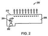
発光ダイオード(LED)等の点光源を使用して、平面的で均一に放射する照明面を作成することは困難である。LEDから放射される光を均一に照明面全体に分散するには複雑な光学的構造が必要である。このような構造の実施例は、点光源をガイドの端部で受容し、光をガイドの表面上に均一に分散する導光板である。図1に示されるように、エッジ照明される構造100は、光104を導光板108の端部106へ伝達するサイド放射の点光源102を使用することができる。導光板108は、光104を頂面110に分散する。光源102は、導光板108から分離される。(background)
It is difficult to create a planar and uniformly illuminating surface using a point light source such as a light emitting diode (LED). A complex optical structure is required to uniformly distribute the light emitted from the LED over the entire illumination surface. An example of such a structure is a light guide plate that receives a point light source at the end of the guide and distributes the light uniformly on the surface of the guide. As shown in FIG. 1, the edge-
しかしながら、構造を照明し得る光源の数は、導光板端部の長さおよび光源の寸法により、制限される。ガイドの表面面積が増加するにつれて、ガイドの表面上に一定の照明を維持するには、導光板端部に物理的に適合できるよりも多くの光源が必要になる可能性があり、最終的に表面面積の上限を設定する。その上に、エッジ照明される導光板は、サイド放射で、予めパッケージ化された光源が必要で、それにより、利用され得る光源の数および種類を制限する。さらに、サイド放射の光源からの光を導光板のエッジに結合するために必要な構造は、平面照明システムの小型化を妨げ得る。任意に大型に作成されることが可能で、かつ広範囲の光源を利用し得る平面照明システムに対する、および予めパッケージ化された光源を利用することができる均一に放射する平面照明面に対する必要性が明らかに存在する。 However, the number of light sources that can illuminate the structure is limited by the length of the light guide plate ends and the dimensions of the light sources. As the surface area of the guide increases, maintaining constant illumination on the surface of the guide may require more light sources than can physically fit at the end of the light guide plate, and eventually Set the upper limit of the surface area. Moreover, edge illuminated light guide plates require side-radiated, pre-packaged light sources, thereby limiting the number and type of light sources that can be utilized. Furthermore, the structure required to couple light from the side-emitting light source to the edge of the light guide plate can hinder downsizing of the planar illumination system. Clearly, there is a need for flat illumination systems that can be made arbitrarily large and that can utilize a wide range of light sources, and for uniformly emitting flat illumination surfaces that can utilize prepackaged light sources. Exists.
複数の導光板から構築される平面照明面は、隣接の導光板間の境界または「ステッチ」で不均一の光強度を示し得る。例えば、導光板のエッジは、不均一であり得て、非発光の隙間が導光板間に形成することを可能にする。加えて、2つの隣接する導光板中の光の伝搬方向は異なり得て、境界で光放射の不均一なパターンを生成する。最後に、相互に重なり合うタイルは、迷光が重複域で漏れることを可能にし得る。複数の導光要素から組み立てられ、かつ均一な光を放射する平面照明面に対する必要性が明らかに存在する。 Planar illumination surfaces constructed from multiple light guide plates may exhibit non-uniform light intensity at the boundary or “stitch” between adjacent light guide plates. For example, the edges of the light guide plates can be non-uniform, allowing non-light emitting gaps to form between the light guide plates. In addition, the propagation direction of light in two adjacent light guide plates can be different, producing a non-uniform pattern of light emission at the boundary. Finally, tiles that overlap each other may allow stray light to leak in the overlap area. There is clearly a need for a planar illumination surface assembled from a plurality of light guide elements and emitting uniform light.
(概要)
本発明は、LED光源を含むタイル状の照明ユニットを備える平面照明領域を形成することにより、従来技術の照明面により課せられた制約を克服する。多様な実施形態において、各平面照明ユニットは、導光要素とLED光源とを含む。例えば、ランベルト光源等の任意の上方放射光源が使用され得る。得られる平面照明領域は、同等の従来技術の構造よりも少ない集積離散平面照明ユニットを使用することができ、したがって全体的なコストを削減する。(Overview)
The present invention overcomes the limitations imposed by prior art illumination surfaces by forming a planar illumination area with a tiled illumination unit that includes an LED light source. In various embodiments, each planar lighting unit includes a light guide element and an LED light source. For example, any upward emitting light source such as a Lambertian light source can be used. The resulting planar illumination area can use fewer integrated discrete planar illumination units than comparable prior art structures, thus reducing overall costs.
さらに、本発明は、例えば、LED等の離散発光要素のために、光学パッケージの少なくとも一部を形成する導光要素を使用することにより、予めパッケージ化された(例えば、ベアダイ)光源を使用して、平面域を照明することを可能にする。このように、導光要素は、光源を導光板のエッジに付設する必要性を克服する。例えば、ランベルト光源等の任意の上方放射光源が使用され得る。得られる平面照明領域は、同等の従来技術の構造よりも少ない集積離散平面照明ユニットを使用することができ、したがって全体的なコストを削減する。 Furthermore, the present invention uses a prepackaged (eg, bare die) light source by using a light guide element that forms at least part of an optical package, eg, for discrete light emitting elements such as LEDs. It is possible to illuminate the plane area. Thus, the light guide element overcomes the need to attach a light source to the edge of the light guide plate. For example, any upward emitting light source such as a Lambertian light source can be used. The resulting planar illumination area can use fewer integrated discrete planar illumination units than comparable prior art structures, thus reducing overall costs.
本発明に従う構造では、導光要素から分離するLEDサブアセンブリプラットフォームが関与し得る。LEDサブアセンブリは、LED光源に電流を供給する電気的インターフェース、光源から離れる熱伝導を可能にする熱インターフェース、および/または所望の表面または他の照明源への付設のための機械的インターフェース(例えば、平面照明領域がタイル状の複数の光源により形成される場合)を含む、照明に必要なインターフェースの全てを含むことができる。LEDサブアセンブリの構造は、光源に付設する前に、電気要素の組み立ておよび電気接触のハンダ付けも可能にすることができる。このように、本発明に従って、ハンダ付けの高温(例えば、約250℃)に脆弱な光源であっても、このような光源が曝され得る最高温度は、装置の操作温度(例えば、約150℃)であるため利用され得る。 The structure according to the invention may involve an LED subassembly platform that separates from the light guide element. The LED subassembly may include an electrical interface that supplies current to the LED light source, a thermal interface that allows heat conduction away from the light source, and / or a mechanical interface for attachment to a desired surface or other illumination source (e.g., All of the interfaces required for illumination, including a planar illumination area formed by a plurality of tiled light sources. The structure of the LED subassembly can also allow assembly of electrical elements and soldering of electrical contacts prior to attachment to the light source. Thus, according to the present invention, even for light sources that are vulnerable to soldering high temperatures (eg, about 250 ° C.), the maximum temperature at which such light sources can be exposed is the operating temperature of the device (eg, about 150 ° C.). ) Can be used.
各導光要素は、入力結合、集積、伝搬および出力結合の領域を含む集積モノリシック導光板である。入力結合領域は、LED光源から放射される光を収集し、出力結合領域は、平面照明を作成するように光を放射する。光源は、要素の入力結合領域に隣接し得るが、そのエッジに配置される必要はない。1つの導光要素の入力結合領域は、隣接する要素の発光領域により少なくとも部分的に覆われ得る。この様式において、1つの要素の光が当たっていない域は隣接する要素の光が当たっている域を覆うことにより閉塞されるため、必要な数の導光要素をタイル状に配置することにより、任意の所望のサイズの連続照明面が構築され得る。 Each light guide element is an integrated monolithic light guide plate that includes areas for input coupling, integration, propagation and output coupling. The input coupling region collects light emitted from the LED light source, and the output coupling region emits light to create planar illumination. The light source may be adjacent to the input coupling area of the element, but need not be located at its edge. The input coupling area of one light guide element may be at least partially covered by the light emitting area of an adjacent element. In this manner, areas where one element is not exposed to light are occluded by covering areas where adjacent elements are exposed to light, so by arranging the required number of light guiding elements in a tile, A continuous illumination surface of any desired size can be constructed.
加えて、本発明の実施形態は、光の不均一な分布が、発光要素間の境界で閉塞することを防ぐ。例えば、導光要素の側壁は、所望に応じて、光を反射または屈折するように、研磨、湾曲、または90度の角度に設定され得る。屈折率整合材料は、隣接する導光要素の間、および/または導光要素の発光面上に配置され得る。光吸収面は、2つの導光要素が重なり合う領域に設置され得て、導光要素は、重複領域中で変化する配光を放射し得る。 In addition, embodiments of the present invention prevent uneven distribution of light from clogging at the boundaries between light emitting elements. For example, the side walls of the light guide element can be polished, curved, or set at a 90 degree angle to reflect or refract light as desired. The index matching material may be disposed between adjacent light guide elements and / or on the light emitting surface of the light guide element. The light absorbing surface can be placed in a region where two light guide elements overlap, and the light guide element can emit a light distribution that varies in the overlap region.
概して、一局面においては、発光面は、タイル状の構成で配設された複数の離散的で実質的に平坦な発光照明装置を含む。各装置は、発光領域と、光が放射されない非照明領域とを有する。第1の装置の発光領域は、第2の隣接する装置の非照明領域の少なくとも一部を閉塞する。各装置は、空間的に別個の入力結合領域と出力結合領域とを含む導光要素を含み、それにより、入力結合領域に入射する光は、出力結合領域から放射するために光要素内で実質的に保持される。 In general, in one aspect, the light emitting surface includes a plurality of discrete, substantially flat light emitting lighting devices arranged in a tiled configuration. Each device has a light emitting area and a non-illuminated area where no light is emitted. The light emitting area of the first device closes at least part of the non-illuminated area of the second adjacent device. Each device includes a light guide element that includes a spatially distinct input coupling area and an output coupling area, so that light incident on the input coupling area is substantially within the optical element for emission from the output coupling area. Retained.
以下の機能のうち1つ以上が含まれ得る。各装置は、少なくとも1つのLEDを含み得て、LEDから放射される光は、入力結合領域の導光要素に結合され得る。LEDは、ランベルト光源であり得る。各照明装置は、単一のLED、複数のLED、一対の対向するLED、または複数の隣接するLEDを含むことができる。各導光要素は、その出力結合領域がその入力結合領域を隠すように、折り畳み式構造を有することができる。発光面は、可撓性であり得る。導光要素は、入力結合領域で受容される多方向光のかなりの割合を出力結合領域に向かって方向付けるための集積領域をさらに含むことができる。導光要素は、出力結合領域に到達する前に、集積領域からの光が通過する伝搬領域をさらに含むことができる。面は、複数のピクセルを含み、発光照明装置の近接かつ前面に配置される、液晶表示パネルをさらに含む。概して、別の局面においては、複数の導光要素から平面発光面を形成する方法は、第1および第2の導光要素を提供するステップを含む。第1の導光要素は、第1の入力結合領域と、そこから空間的に分離された第1の出力結合領域とを備え、それにより、第1の入力結合領域に入射する光は、第1の出力結合領域から放射するために、第1の導光要素内で実質的に保持される。同様に、第2の導光要素は、第2の入力結合領域と、そこから空間的に分離された第2の出力結合領域とを備え、それにより、第2の入力結合領域に入射する光は、第2の出力結合領域から放射するために、第2の導光要素内で実質的に保持される。第2の導光要素の一部は、重複領域を形成するように、第1の導光要素の一部の上に重ね合わされる。第2の入力結合領域に入射する光は、第2の出力結合領域から放射するために、第2の導光要素内で実質的に保持される。重複領域は、少なくとも第1の入力結合領域と、第1の入力結合領域を完全に閉塞する第2の出力結合領域の少なくとも一部とを含む。 One or more of the following functions may be included. Each device may include at least one LED, and light emitted from the LED may be coupled to a light guide element in the input coupling region. The LED can be a Lambertian light source. Each lighting device can include a single LED, multiple LEDs, a pair of opposing LEDs, or multiple adjacent LEDs. Each light guide element can have a foldable structure such that its output coupling area conceals its input coupling area. The light emitting surface can be flexible. The light guide element can further include an integrated region for directing a significant percentage of the multi-directional light received at the input coupling region toward the output coupling region. The light guide element may further include a propagation region through which light from the integration region passes before reaching the output coupling region. The surface further includes a liquid crystal display panel that includes a plurality of pixels and is disposed adjacent to and in front of the light emitting lighting device. In general, in another aspect, a method of forming a planar light emitting surface from a plurality of light guide elements includes providing first and second light guide elements. The first light guide element includes a first input coupling region and a first output coupling region spatially separated therefrom, whereby light incident on the first input coupling region is In order to radiate from one output coupling region, it is substantially retained within the first light guide element. Similarly, the second light guide element comprises a second input coupling region and a second output coupling region spatially separated therefrom, whereby light incident on the second input coupling region Is substantially retained in the second light guide element for radiating from the second output coupling region. A part of the second light guide element is superimposed on a part of the first light guide element so as to form an overlapping region. Light incident on the second input coupling region is substantially retained in the second light guide element for emission from the second output coupling region. The overlap region includes at least a first input coupling region and at least a portion of a second output coupling region that completely occludes the first input coupling region.
以下の機能のうち1つ以上が含まれ得る。第2の出力結合領域からの光は、第2の導光要素の任意の非照明領域を完全に閉塞することができる。第1の導光要素は、第1の伝搬領域と第1の集積領域とをさらに含むことができ、第2の出力結合領域は、第1の伝搬領域と第1の集積領域とを閉塞することもできる。第1の導光要素は、第1の縞状の要素の一部であり得て、第2の導光要素は、第2の縞状の要素の一部であり得る。第1および第2の縞状の要素は、非対称であり、隣接して配設され得て、および/または対称であり、追加の対称の縞状の要素の行列内で折り合わされ得る。離散光源は、LEDであり得て、ランベルト光源の場合がある。各照明装置は、単一のLED、複数のLED、一対の対向するLED、または複数の隣接するLEDを含むことができる。 One or more of the following functions may be included. Light from the second output coupling region can completely occlude any non-illuminated region of the second light guide element. The first light guide element may further include a first propagation region and a first integration region, and the second output coupling region occludes the first propagation region and the first integration region. You can also The first light guide element may be part of the first striped element and the second light guide element may be part of the second striped element. The first and second striped elements may be asymmetric, arranged adjacent to each other, and / or symmetric and folded within a matrix of additional symmetric striped elements. The discrete light source may be an LED and may be a Lambertian light source. Each lighting device can include a single LED, multiple LEDs, a pair of opposing LEDs, or multiple adjacent LEDs.
本方法は、追加の導光要素へ拡張することができる。例えば、本方法は、第2の重複領域を形成するように、第2の導光要素の少なくとも一部の上に第3の導光要素の少なくとも一部を重ね合わせるステップをさらに含むことができる。第3の導光要素は、第3の入力結合領域とそこから空間的に分離された第3の出力結合領域とを含むことができ、それにより、第3の入力結合領域に入射する光は、第3の出力結合領域から放射するために、第3の導光要素内で実質的に保持される。第2の重複領域は、第3の出力結合領域の少なくとも一部を含むことができる。各導光要素は、サブアセンブリプラットフォームおよび導光要素の融合により形成されるソケットを含む照明装置を使用して、照明され得る。ソケットは、導光要素の入力結合領域に結合された離散光源を含むことができる。 The method can be extended to additional light guide elements. For example, the method can further include overlaying at least a portion of the third light guide element over at least a portion of the second light guide element to form a second overlap region. . The third light guide element may include a third input coupling region and a third output coupling region spatially separated therefrom, such that light incident on the third input coupling region is , Substantially retained within the third light guide element for radiating from the third output coupling region. The second overlapping region can include at least a portion of the third output coupling region. Each light guide element may be illuminated using a lighting device that includes a socket formed by the fusion of the subassembly platform and the light guide element. The socket can include a discrete light source coupled to the input coupling region of the light guide element.
本方法は、各々入力結合領域とそこから空間的に分離された出力結合領域とを備える、追加の導光要素を提供するステップをさらに含むことができる。入力結合領域に入射する光は、出力結合領域から放射するために、対応する導光要素内で実質的に保持され得る。各追加の導光要素の一部は、出力結合領域が各入力結合領域を閉塞するように、隣接する導光要素の一部の上に重ね合わされ得る。重ね合わせるステップは、導光要素を屈曲するステップを含むことができる。 The method can further include providing additional light guide elements, each comprising an input coupling region and an output coupling region spatially separated therefrom. Light incident on the input coupling region can be substantially retained in the corresponding light guide element for emission from the output coupling region. A portion of each additional light guide element may be overlaid on a portion of the adjacent light guide element such that the output coupling region occludes each input coupling region. The overlapping step can include bending the light guide element.
概して、別の局面においては、離散的で実質的に平坦な発光照明装置は、空間的に別個の入力結合および出力結合領域と、入力結合領域に光学的に結合される少なくとも1つの光源とを含む、導光要素を備える。入力結合領域は、その側面に沿って出力結合領域に隣接し、それを覆って折り畳まれる。入力結合領域に入射する光は、出力結合領域から放射するために、導光要素内で実質的に保持される。 In general, in another aspect, a discrete, substantially flat light-emitting illuminating device includes a spatially separate input and output coupling region and at least one light source that is optically coupled to the input coupling region. Including a light guide element. The input coupling area is folded along and over the side of the output coupling area. Light incident on the input coupling region is substantially retained within the light guide element for emission from the output coupling region.
以下の機能のうち1つ以上が含まれ得る。第2の入力結合領域は、その第2の側面に沿って出力結合領域に隣接し、それを覆って折り畳まれ得る。第2の入力結合領域に入射する光は、出力結合領域から放射するために、導光要素内で実質的に保持され得る。少なくとも1つの光源は、第2の入力結合領域に光学的に結合され得る。入力結合領域と第2の入力結合領域は、異なる光源に光学的に結合される。入力結合領域および第2の入力結合領域は、少なくとも1つの光源で同一に光学的に結合され得る。 One or more of the following functions may be included. The second input coupling region may be folded along and over the second side of the output coupling region. Light incident on the second input coupling region can be substantially retained in the light guide element for emission from the output coupling region. At least one light source may be optically coupled to the second input coupling region. The input coupling region and the second input coupling region are optically coupled to different light sources. The input coupling region and the second input coupling region may be optically coupled identically with at least one light source.
概して、別の局面においては、複数の導光要素から平面発光面を形成する方法は、第1の入力結合領域と第1の出力結合領域とを含む、第1の導光要素を提供するステップを含む。第1の入力結合領域と第1の出力結合領域は、空間的に別個で、第1の入力結合領域に入射する光は、第1の出力結合領域から放射するために、導光要素内で実質的に保持される。第2の入力結合領域と第2の出力結合領域とを含む、第2の導光要素は、第1の導光要素に隣接して提供される。第2の入力結合領域と第2の出力結合領域は、空間的に別個である。第2の入力結合領域に入射する光は、第2の出力結合領域から放射するために、導光要素内で実質的に保持される。第1の出力結合領域は、第1の入力結合領域を閉塞し、第2の出力結合領域は、第2の入力結合領域を閉塞するため、隣接する第1および第2の導光要素は、光の連続面を放射する。 In general, in another aspect, a method of forming a planar light emitting surface from a plurality of light guide elements provides a first light guide element that includes a first input coupling region and a first output coupling region. including. The first input coupling region and the first output coupling region are spatially separate, and light incident on the first input coupling region is emitted within the light guide element to radiate from the first output coupling region. Substantially retained. A second light guide element including a second input coupling region and a second output coupling region is provided adjacent to the first light guide element. The second input coupling region and the second output coupling region are spatially distinct. Light incident on the second input coupling region is substantially retained in the light guide element for emission from the second output coupling region. Since the first output coupling region closes the first input coupling region and the second output coupling region blocks the second input coupling region, the adjacent first and second light guide elements are Radiates a continuous surface of light.
以下の機能のうち1つ以上が含まれ得る。導光要素は可撓性であり得る。本方法は、第1の出力結合領域を第1の入力結合領域を覆って折り畳むステップと、第2の出力結合領域を第2の入力結合領域を覆って折り畳むステップとをさらに含むことができる。 One or more of the following functions may be included. The light guide element may be flexible. The method can further include folding the first output coupling region over the first input coupling region and folding the second output coupling region over the second input coupling region.
概して、別の局面においては、照明源は、サブアセンブリプラットフォームおよび導光要素の融合により形成されるソケットと、ソケット内に受容される離散光源とを含む。 In general, in another aspect, an illumination source includes a socket formed by the fusion of a subassembly platform and a light guide element, and a discrete light source received within the socket.
以下の機能のうち1つ以上が含まれ得る。離散光源は、サブアセンブリプラットフォーム上に配置され、かつ電気的に接続されるLEDダイを含むことができる。導光要素は、サブアセンブリプラットフォームを覆って配置され、かつこれと直接接触することができ、LEDダイ用のパッケージの少なくとも一部として機能することができる。封入材料は、LEDダイと導光要素の間に配置され、これらと直接接触することができる。サブアセンブリプラットフォームは、輪郭電気接続を含むことができる。離散光源は、サブアセンブリプラットフォームに熱的に接続され得る。サブアセンブリプラットフォームは、照明源を構造に接続するための機械的インターフェースを含むことができる。 One or more of the following functions may be included. The discrete light source can include an LED die disposed on the subassembly platform and electrically connected. The light guide element is disposed over and in direct contact with the subassembly platform and can function as at least part of a package for the LED die. The encapsulating material is disposed between the LED die and the light guide element and can be in direct contact with them. The subassembly platform can include contour electrical connections. The discrete light source may be thermally connected to the subassembly platform. The subassembly platform can include a mechanical interface for connecting the illumination source to the structure.
導光要素は、空間的に別個の入力結合と出力結合領域とを含むことができる。離散光源により入力結合領域に入射される光は、出力結合領域から放射するために、導光要素内で実質的に保持され得る。離散光源は、最上部放射型および/またはランベルト光源であり得る。概して、別の局面においては、照明装置を形成する方法は、サブアセンブリプラットフォームの凹部中に離散光源を提供するステップを含む。サブアセンブリプラットフォームは、導光要素に接合され、それにより、その中に離散光源が配置される、閉鎖型ソケットを形成する。 The light guide element can include a spatially separate input coupling and output coupling region. Light incident on the input coupling region by the discrete light source can be substantially retained in the light guide element for emission from the output coupling region. The discrete light source may be a top-emitting and / or Lambertian light source. In general, in another aspect, a method of forming a lighting device includes providing a discrete light source in a recess of a subassembly platform. The subassembly platform is joined to the light guide element, thereby forming a closed socket in which the discrete light sources are disposed.
以下の機能のうち1つ以上が含まれ得る。封入材料が閉鎖型ソケットの任意の自由体積を占有するように、離散光源の上に封入材料が提供され得る。サブアセンブリプラットフォームは、離散光源を提供するステップの前に組み立てられ得る。サブアセンブリプラットフォームを導光要素に接合するステップは、約85℃より低い温度で少なくとも部分的に実施され得て、ベアダイLEDであり得る、離散光源は、約85℃より低い温度で少なくとも部分的に操作され得る。 One or more of the following functions may be included. An encapsulant can be provided over the discrete light source such that the encapsulant occupies any free volume of the closed socket. The subassembly platform may be assembled before the step of providing a discrete light source. The step of bonding the subassembly platform to the light guide element may be performed at least partially at a temperature below about 85 ° C., and the discrete light source may be at least partially at a temperature below about 85 ° C., which may be a bare die LED. Can be manipulated.
電流は、サブアセンブリプラットフォームを通して、離散光源に提供され得る。それにより、離散光源は、光を導光要素に放射することができる。離散光源により生成される熱は、サブアセンブリプラットフォームを通して、消散され得る。光は、導光要素の頂面全体で実質的に均一に放射され得る。 Current can be provided to the discrete light source through the subassembly platform. Thereby, the discrete light source can emit light to the light guide element. The heat generated by the discrete light source can be dissipated through the subassembly platform. The light can be emitted substantially uniformly across the top surface of the light guide element.
概して、別の局面においては、導光要素は、光源から多方向光を受容するための入力結合領域と、導光要素から光を放射するための出力結合領域とを含む。集積領域は、出力結合領域とは反対側の入力結合領域に近接し、入力結合領域からの多方向光を出力結合領域に向かって方向付ける。 In general, in another aspect, the light guide element includes an input coupling region for receiving multidirectional light from the light source and an output coupling region for emitting light from the light guide element. The integration region is proximate to the input coupling region opposite the output coupling region and directs multi-directional light from the input coupling region toward the output coupling region.
以下の機能のうち1つ以上が含まれ得る。集積領域は、放物線形状を有することができ、放物線形状の中心は、入力結合領域の中心であり得る。集積領域は、入力結合領域からオフセットされ得る。集積領域に当たる光の角度は、全反射の角度よりも大きいことがあり得る。側壁は、反射性被膜を含むことができる。集積領域に伝達される光は、出力結合領域に向かって実質的または完全に反射され得る。集積領域から反射される光は、入力結合領域から出力結合領域へ直接伝達される光と結合して、出力結合領域内で光強度の均一な分布を生成することができる。 One or more of the following functions may be included. The integration region can have a parabolic shape, and the center of the parabolic shape can be the center of the input coupling region. The integration region can be offset from the input coupling region. The angle of light striking the integration region can be greater than the angle of total reflection. The sidewall can include a reflective coating. Light transmitted to the integration region can be substantially or completely reflected toward the output coupling region. Light reflected from the integration region can be combined with light transmitted directly from the input coupling region to the output coupling region to produce a uniform distribution of light intensity within the output coupling region.
概して、別の局面においては、導光要素は、入力結合領域、伝搬領域、出力結合領域、頂面、および側壁を含む。光は、入力結合領域で導光要素により受容され、伝搬領域を通して伝達され、出力結合領域により放射される。頂面および側壁は、丸い角により接合される。丸い角は、その上の入射光を伝達し、頂面および側壁は、その上の入射光を反射する。丸い角は、出力結合領域内にあり得て、側壁は、研磨され得る。 In general, in another aspect, the light guide element includes an input coupling region, a propagation region, an output coupling region, a top surface, and a sidewall. Light is received by the light guide element at the input coupling region, transmitted through the propagation region, and emitted by the output coupling region. The top and side walls are joined by rounded corners. The rounded corners carry incident light thereon, and the top and sidewalls reflect incident light thereon. Round corners can be in the output coupling region and the sidewalls can be polished.
概して、別の局面においては、導光要素は、入力結合領域、伝搬領域、出力結合領域、頂面、および側壁を含む。光は、入力結合領域で導光要素により受容され、伝搬領域を通して伝達され、出力結合領域により放射される。頂面と側壁は90度の角により接合され、頂面、側壁および90度の角はその上の入射光を反射する。90度の角は、出力結合領域中にあり得て、側壁は研磨され得る。 In general, in another aspect, the light guide element includes an input coupling region, a propagation region, an output coupling region, a top surface, and a sidewall. Light is received by the light guide element at the input coupling region, transmitted through the propagation region, and emitted by the output coupling region. The top surface and the side wall are joined by a 90 degree angle, and the top surface, the side wall, and the 90 degree angle reflect incident light thereon. The 90 degree corner can be in the output coupling region and the sidewalls can be polished.
概して、別の局面において、平面照明領域は、第1の出力結合領域を含む第1の導光要素と、第2の出力結合領域を含む第2の導光要素とを含む。第2の出力結合領域の少なくとも一部は、第1の出力結合の少なくとも一部に重なり合って、ある域を有する重複領域を画定する。重複領域は、域上に実質的に均一な光出力を放射する。 In general, in another aspect, a planar illumination region includes a first light guide element that includes a first output coupling region and a second light guide element that includes a second output coupling region. At least a portion of the second output coupling region overlaps at least a portion of the first output coupling region to define an overlapping region having a region. The overlapping area emits a substantially uniform light output over the area.
以下の機能のうち1つ以上が含まれ得る。重複領域の光出力は、第1および第2の出力結合領域の光出力と10%以内の差があり得る。重複領域と、第1および第2の出力結合領域との間の光出力の変化は緩やかであり得る。第1の出力結合領域は、その中に光散乱要素を含むことができ、第1および第2の出力結合領域は部分的にだけ重なり合うことができる。重複領域外の光散乱要素の密度は、重複領域内の光散乱要素の密度よりも大きいことがあり得る。重複領域内の光散乱要素の密度は、一方向に沿って減少することができる。 One or more of the following functions may be included. The light output of the overlap region can be within 10% of the light output of the first and second output coupling regions. The change in light output between the overlap region and the first and second output coupling regions can be gradual. The first output coupling region can include a light scattering element therein, and the first and second output coupling regions can only partially overlap. The density of light scattering elements outside the overlapping region can be greater than the density of light scattering elements within the overlapping region. The density of light scattering elements in the overlapping region can decrease along one direction.
第2の出力結合領域は、重複領域において透明であり得る。第1の出力結合領域から放射される光は、重複領域中の第2の出力結合領域を通過することができる。第1および第2の出力結合領域は、部分的にのみ重なり合うことができ、平面照明領域は、第3の出力結合領域を含む、第3の導光要素をさらに含むことができる。第3の出力結合領域の一部は、第2の出力結合領域の第2の一部に重なり合って、第2の領域を有する第2の重複領域を画定することができる。第2の重複領域は、第2の領域上に実質的に均一な光出力を放射することができる。 The second output coupling region may be transparent in the overlapping region. Light emitted from the first output coupling region can pass through the second output coupling region in the overlap region. The first and second output coupling regions can only partially overlap, and the planar illumination region can further include a third light guide element that includes a third output coupling region. A portion of the third output coupling region can overlap a second portion of the second output coupling region to define a second overlapping region having a second region. The second overlapping region can emit a substantially uniform light output over the second region.
第1の導光要素は、非垂直の側壁を含むことができ、第2の導光要素は、重複領域内に第2の補完的な非垂直の側壁を含むことができる。平面照明領域の頂面は、実質的に平坦であり得る。追加の導光要素は、第1および第2の導光要素とともに、第1および第2の方向に延材する配列を形成することができ、導光要素は、第1の方向に重なり合うことができて、第2の方向には重なり合うことができないか、または第1および第2の両方の方向で重なり合うことができる。重複領域は、光吸収材料を含むことができる。 The first light guide element can include non-vertical sidewalls and the second light guide element can include a second complementary non-vertical sidewall in the overlap region. The top surface of the planar illumination area can be substantially flat. The additional light guide elements can form an array extending with the first and second light guide elements in the first and second directions, and the light guide elements can overlap in the first direction. And can not overlap in the second direction, or can overlap in both the first and second directions. The overlapping region can include a light absorbing material.
概して、別の局面においては、平面照明領域を形成する方法は、第1の出力結合領域を含む第1の導光要素を提供するステップを含む。第1の導光要素の少なくとも一部は、第2の出力結合領域を含む第2の導光要素に重ね合わされ、それにより、第1の出力結合領域の少なくとも一部と、第2の出力結合領域とを含む重複領域を形成する。重複領域は、実質的に均一な光出力を放射する。 In general, in another aspect, a method of forming a planar illumination region includes providing a first light guide element that includes a first output coupling region. At least a portion of the first light guide element is superimposed on a second light guide element that includes a second output coupling region, thereby providing at least a portion of the first output coupling region and a second output coupling. An overlapping region including the region is formed. The overlapping region emits a substantially uniform light output.
概して、別の局面においては、平面照明領域は、それぞれ、第1および第2の側壁を含む、第1および第2の導光要素を含む。屈折率整合材は、第1および第2の側壁を覆う。屈折率整合材料の屈折率は、第1の導光要素または第2の導光要素のうちの少なくとも1つの屈折率にほぼ等しい。 In general, in another aspect, a planar illumination region includes first and second light guide elements that include first and second sidewalls, respectively. The refractive index matching material covers the first and second side walls. The refractive index of the index matching material is approximately equal to the refractive index of at least one of the first light guide element or the second light guide element.
以下の機能のうち1つ以上が含まれ得る。第2の側壁は、第1の側壁に隣接することができ、屈折率整合材料は、第1の側壁と第2の側壁との間に位置し得る。第1および第2の導光要素は、重なり合うことができ、屈折率整合材料は、第1および第2の導光要素を覆って、それを覆う円滑面を作成することができる。 One or more of the following functions may be included. The second sidewall can be adjacent to the first sidewall, and the index matching material can be located between the first sidewall and the second sidewall. The first and second light guide elements can overlap and the refractive index matching material can cover the first and second light guide elements and create a smooth surface over them.
概して、別の局面においては、平面照明領域は、それぞれ、第1および第2の研磨された側壁を含む、第1および第2の導光要素を含む。第2の研磨された側壁は、第1の研磨された側壁に隣接する。第2の導光要素は、第1の研磨された側壁および第2の研磨された側壁を通じて、第1の導光要素から光を受容する。屈折率整合材料は、第1の側壁と第2の側壁との間に位置し得て、屈折率整合材料の屈折率は、第1の導光要素または第2の導光要素のうちの少なくとも1つの屈折率にほぼ等しい。 In general, in another aspect, a planar illumination region includes first and second light guide elements that include first and second polished sidewalls, respectively. The second polished sidewall is adjacent to the first polished sidewall. The second light guide element receives light from the first light guide element through the first polished side wall and the second polished side wall. The refractive index matching material may be located between the first sidewall and the second sidewall, and the refractive index of the refractive index matching material is at least one of the first light guide element or the second light guide element. It is approximately equal to one refractive index.
これらおよび他の目的は、本明細書に開示される本発明の利点および特徴に加えて、以下の説明、添付の図面および請求項を参照することにより、より明らかになる。さらに、本明細書に説明される多様な実施形態の特徴は、相互に排他的ではなく、多様な組み合わせおよび置換において存在し得ることを理解されたい。 These and other objects will become more apparent by reference to the following description, accompanying drawings and claims, in addition to the advantages and features of the invention disclosed herein. Further, it should be understood that the features of the various embodiments described herein are not mutually exclusive and may exist in various combinations and substitutions.
図面においては、同様な参照文字は、概して、様々な表示全体で同一の部分を指す。以下の説明においては、本発明の多様な実施形態は以下の図面を参照して説明される。
(詳細な説明)
(1.基本的設計)
本明細書には、1つ以上の離散平面照明ユニットに基づいて平面照明を組み立てるための方法およびシステムの多様な実施形態、様々なタイプの導光要素およびLEDサブアセンブリの様々な実施形態、および平面照明ユニットのタイルの間の不均一の「ステッチ」効果を排除するための方法およびシステムの多様な実施形態が説明される。(Detailed explanation)
(1. Basic design)
The present specification includes various embodiments of methods and systems for assembling flat lighting based on one or more discrete flat lighting units, various embodiments of various types of light guide elements and LED subassemblies, and Various embodiments of methods and systems for eliminating non-uniform “stitch” effects between tiles of a planar lighting unit are described.
本発明の利点は、多様な実施形態において、上方放射(例えば、ランベルト)光源を利用できることである。図2は、一般的に、導光板208内に完全に埋め込まれた集積型上方放射光源202を備えるモノリシック構造200を示す。光源202は、ランベルト光分布を有することができ、光204は、その面210を通して放射するために、導光板208内で実質的に保持される。 An advantage of the present invention is that, in various embodiments, an upward emitting (eg, Lambertian) light source can be utilized. FIG. 2 shows a
概して、本発明は、光源が少なくとも部分的に(および通常は完全に)埋め込まれるモジュール式導光要素を利用し、図2に示される光の維持および放射動作を促進する。要素はタイル状に配置されて、任意のサイズの均一な照明面を促進する。代表的なタイル状の平面照明ユニット300が、図3では斜視図および図4では断面図に示される。示された平面照明ユニット300は、一対の対向するLEDサブアセンブリモジュール302と、導光要素304とを含む。以下に詳細が説明されるように、導光要素304は、光の捕捉、保持および放射を最適化する、多様な領域、例えば、入力結合領域306、集積領域308、伝搬領域310および出力結合領域312を含むことができる。各LEDサブアセンブリモジュール302は、所望に応じて、以下に詳細を説明するように、導光要素304の入力結合領域306内に少なくとも部分的にパッケージ化されたLED光源を含む。 In general, the present invention utilizes a modular light guide element in which the light source is at least partially (and usually fully) embedded to facilitate the light maintenance and emission operations shown in FIG. The elements are tiled to promote a uniform illumination surface of any size. A typical tiled
光は、ランベルト光源であり得る、LED光源から上方へ、導光要素304の入力結合領域306内に放射され得て、この場合、光は横方向に伝搬する(すなわち、導光板304の厚さ内に限定される)。導光要素304の入力結合および集積領域306、308は、光源から光を有効に集め、最小限の損失で、伝搬領域310へ向かって方向付ける。具体的には、集積領域308は、入力結合領域306で受容した多方向光のかなりの割合を出力結合領域312に向かって配向させる。集積領域308からの光は、伝搬領域310を横断して、発光出力結合領域312まで進み、光源の所望の機能に適した分布で、出力結合領域312と伝搬領域310との間のインターフェース314に到達する。例えば、照明領域全体に均一な光放射を取得するためには、インターフェース314全体で光を均一に分布することが好ましい。インターフェース314は、通常は、はっきりした境界ではなく、例えば、別個の区域で発生する拡散粒子の密度における変化、により確立される段階的な遷移である。以下に説明される出力結合サブ領域も同様である。 Light can be emitted upwards from the LED light source, which can be a Lambertian light source, into the
出力結合領域312において、光は導光板から放射され、この結果、特定の用途に依存する所望の特性を備える平面照明となる。例えば、出力結合領域全体で実質的に均一な照明は、バックライト用途では好まれ得る。(「実質的に均一」とは、出力強度において10%以内の変動を意味する。)モノリシック導波およびこれらの製造方法は、例えば、上記参照出願第’110号(「Waveguide Sheet and Method for Manufacturing the Same」)において詳細に説明される。 In the
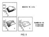
本発明の実施形態による平面照明システムにより示された例示的な特性は、図5に示される。図5に示された動作を有する平面照明システムは、離散光源として、2つのRGB中型LEDチップを含み、システムの厚さは約5mmである。これらの平面照明システムは、平方メートルあたり約2060カンデラ(ニト)の輝度を示し、輝度の不均一性は±約6%である。(0.254、0.240)の(x、y)色座標の場合、色の均一性(Δx、Δy)は約(±0.008、±0.006)であり得る。 Exemplary characteristics exhibited by a planar illumination system according to an embodiment of the present invention are shown in FIG. The flat illumination system having the operation shown in FIG. 5 includes two RGB medium LED chips as discrete light sources, and the thickness of the system is about 5 mm. These flat lighting systems exhibit a brightness of about 2060 candela (nits) per square meter with a brightness non-uniformity of ± about 6%. For (x, y) color coordinates of (0.254, 0.240), the color uniformity (Δx, Δy) may be about (± 0.008, ± 0.006).
図3および4を再度参照すると、入力結合領域306の円筒形状は、図示を目的とするものであって、他の形状も使用され得る。例えば、入力結合領域306は、環状または円筒状の輪郭を有する2つの領域を含むことができる。例えば、白、単一色、赤緑青(RGB)または赤外(IR)光源、ならびにベアダイまたはパッケージLEDのどちらか等の1つ以上の光源が、入力結合領域306の裏面に取り付けられ得る。これらの光源は、光を導光要素304に結合するように、LEDにより放射された光の方向を変更する、入力結合領域306を通して導光板に結合される光を放射する。 Referring again to FIGS. 3 and 4, the cylindrical shape of the
導光要素304に結合されると、光は、入力結合領域306の周辺部に沿って全方向に放射され得る。入力結合は、2008年4月29日に出願された米国特許出願第12/155、090号「Method and Device for Providing Circumferential Illumination」に説明され、その全体が本明細書に参考として援用される。例えば、入力結合領域306は、光漏斗の形を取り得る。漏斗は、1つ以上の発光要素から光を受容し、かつ光を伝搬領域310へ伝達する。漏斗は、1つ以上のLEDから生成された光を入力面を通して受容し、内部体積内で分布し、出力面を通して放射する、面放射導波管または面放射共発振器の形を取り得る。光学的損失を防止または軽減するには、入力結合領域306および/または集積領域308は、1つ以上の反射体(例えば、エッジ反射体)を含むことができる。 When coupled to the
出力結合領域312は、入力結合領域306の片側にのみ位置し得るため、出力結合領域312の反対側316上の入力結合領域306から放射される光は、出力結合領域312に向けて方向を変更され得る。この方向変更は、集積領域308で発生し得て、以下に詳細を説明するように、集積体が光を出力結合領域312へ向かって方向付けることができる。一実施形態において、例えば、2つのLEDと2つの集積体等、各LEDに対して集積体が1つ存在する。図3においては、放物線形状の集積領域308の実施形態が示されるが、他の形状も使用され得る。集積領域308により形成される放物線の中心は、入力結合領域306の中心であり得る。 Because the
伝搬領域310は、入力結合領域306および集積領域308から放射された光が、出力結合領域312に向かって自由に伝搬することを可能にする。出力結合領域312において、光は、平面照明ユニット300から外界へ上方方向に(318で示されるように)曲げられる。この光は、次に、例えば、LCDバックライト用途における表面等の複数のタイル状の照明ユニット300により形成されるより大型の照明面の平面セグメントを照明することができる。出力結合領域312は、図3においては正方形の形状で表されるが、図示の目的のために、3つの矩形サブ領域320、322、324として示される。これらのサブ領域320、322、324は、別々の領域ではなく、一実施形態においては、出力結合領域312内の分散粒子の代表的な分布を示す。これらの粒子は、通常は2方向以上に光放射を散乱する、散乱体として機能することにより、光の放射を促進する。作用角が臨界角未満であるように、光が粒子により散乱すると、全反射が発生せず、散乱した光は、方向318に沿って出力結合領域312の表面を通して放射される。
光散乱粒子は、例えばガラスのビーズ等のビーズ、または他のセラミック粒子、ゴム粒子、シリカ粒子、BaSO4またはTiO2等の無機物質を本質的に含有または構成される粒子、蛍光材料を本質的に含有または構成される粒子(以下に詳細を説明)等であり得る。実施形態においては、光散乱粒子は、実質的に非蛍光性または完全に非蛍光性でもある。このような非蛍光性粒子は、粒子に当たるどの光の波長も変換せずに、ただ光を散乱するだけである。「光散乱粒子」という用語は、このような物体が光を散乱することができる場合、中核構造が作製される導波管材料に埋め込まれる固体以外の物体も指すことができる。適切な固体以外の物体の代表例は、例えば、気泡等の中核構造内の閉鎖空洞、および/または中核構造内に埋め込まれる液滴を含むが、これらに限定されない。光散乱粒子は、リポソーム等の、しかしこれに限定されない、有機または生物的粒子でもあり得る。一部の実施形態においては、ミクロレンズ等の光学要素は、光散乱粒子と同時に、または代わりにも利用される。Light scattering particles are essentially composed of beads, such as glass beads, or other ceramic particles, rubber particles, silica particles, particles that essentially contain or consist of inorganic materials such as BaSO4 or TiO2 , fluorescent materials The particles may be contained or constituted in (described in detail below). In embodiments, the light scattering particles are also substantially non-fluorescent or completely non-fluorescent. Such non-fluorescent particles only scatter light without converting the wavelength of any light impinging on the particles. The term “light scattering particle” can also refer to an object other than a solid that is embedded in the waveguide material from which the core structure is made if such an object can scatter light. Representative examples of suitable non-solid objects include, but are not limited to, closed cavities in the core structure, such as bubbles, and / or droplets embedded in the core structure. The light scattering particles can also be organic or biological particles such as, but not limited to, liposomes. In some embodiments, an optical element, such as a microlens, is utilized simultaneously with or in place of the light scattering particles.
通常、粒子は、出力結合領域312の中心サブ領域322に向かって集中し、すなわち、中心のサブ領域322の粒子濃度は、周辺のサブ領域320、324の濃度を超えるが、通常は、サブ領域の粒子の濃度の遷移は、急激というよりも段階的である。 Usually, the particles are concentrated toward the
同一の拡散材料は、各領域306、308、310、312で使用され得るが、異なる領域の機能に適した異なる濃度で使用され得る。出力結合領域312は、例えば、通常、最大濃度の粒子を含む。集積領域308は、濃度が段階的な粒子を含有し、通常は粒子を含まない伝搬領域310に光を向かって方向付けることができる。 The same diffusing material can be used in each
集積領域308は、導光要素304に結合される光を伝達するため、光は、伝搬領域310に向かって伝搬する。加えて、集積領域308は、入力結合領域306から出力結合領域312への光が、光強度の必要な分布を達成することを可能にし得る。入力結合306、集積308、および伝搬310の領域は、出力結合領域312への入口314で光を均一に分布するように設計され得る。すなわち、出力結合領域312から光を放射するための標準構造は、出力結合領域312への入口314で強度の均一な分布を徹底させることができる。 Since the
図6は、集中領域602、入力結合領域604、および伝搬領域606を含む導光要素600の例示的な部分を示し、これらは、光を均一な様式で出力結合領域に向かって進めることにより、出力結合領域への入口610で光密度の量および均一性を増加させる。集積領域602の導光要素の側面608は、放物線形状および/または反射被膜を有する。集積領域602により形成される放物線の中心は、入力結合領域604の中心であり得る。入力結合領域604で導光要素600に入射する光は、導光要素600で全方向に拡散することができる。図に示されるように、角度の拡散は、大部分は集積領域602に制限され、側壁608での全反射により、伝搬領域606に向かって方向付けられる。臨界角は、この角度以下で側壁608に向かって伝搬する任意の入射光が、最終的に、側壁からの単一または複数の反射を介して、伝搬領域606の入口610に到達するように、例えば、41.8度であり得る。伝搬領域606への入口610で、光強度は、入力結合領域604から伝搬領域606へ直接伝搬する光と、側壁608から反射された光との重畳になる。伝搬領域606の入口610での光強度は、実質的に均一であることが望ましい。このように、光は、伝搬領域606を通じて伝播し、均一な強度分布で、出力結合領域への入口に到達する。 FIG. 6 shows an exemplary portion of a
空気の屈折率は約1であるため、導光要素304は、屈折率が1を超える導波管材料を使用して作製され得る。導光要素304に適切な材料の代表例は、約1.50の屈折率を有するTPU(脂肪族)、約1.58から約1.60までの屈折率を有するTPU(芳香族)、約1.54の屈折率を有する、EMS Grivoryにより提供されるGRILAMID材(例えば、GRILAMID TR90)等の非結晶性ナイロン、約1.46の屈折率を有する、Mitsuiにより提供されるTPX(PMP)材、約1.34の屈折率を有するPVDF、その他の熱可塑性フッ素樹脂、約1.58の屈折率を有する、BASFにより販売されるSTYROLUX(UV安定化)材、約1.5の屈折率を備えるメタクリル酸メチル重合体(PMMA)、および約1.5の屈折率を備えるポリカーボネートを含むが、これらに限定されない。’090用途において説明されるように、導光要素304は、単一の(中核)層から成る、または、中核層が対向する被覆層の間に位置するサンドイッチ構造を有することができる。被覆層(存在する場合)の厚さは、通常、約10μmから約100μmまでである。中核層の厚さは、約400μmから約1300μmまで変化し得る。 Since the refractive index of air is about 1, the
多様な実施形態においては、導光要素304が形成される材料は透明で、少なくともある程度可撓性があり、少なくともいくらかの伸長能力を有し、および/または熱樹脂工程において作製されることが可能である。シリコン等の非常に可撓性の高い材料ならびにPMMAまたはポリカーボネート等のやや可撓性に劣る材料も適切であり得る。選択された材料の屈曲程度は、一連の要素を表面上に組み立てる様式に依存し得る。例えば、一部の組立手順は屈曲をほとんどまたは全く必要としない場合がある。他の実施形態においては、材料は本質的に可撓性がない。比較的硬い材料でも十分に薄い場合は、本明細書に説明される組み立てに適合する十分な機械的可撓性を示すことができる。導波管要素は、組み立てを容易にする屈曲を導入するために、共押出、打ち抜き、共射出成形、または並列溶解を含むがこれらに限定されない任意の適切な技法により製造され得る。 In various embodiments, the material from which the
導光要素304の各領域306、308、310、312は、これらに当たる光の波長を別の波長に変更し、それにより、例えば、光の色を変える、蛍光材料を含むことができる。このように、光源から放射される光の一部の波長を変えることによって、白色光が生成され得る。出力結合領域312への伝搬中、光の部分は、その後異なる波長の光を放射する、蛍光材料により吸収され得る。異なる波長の光は、出力結合領域によりまとめて放射され得て、白色光を形成する。 Each
(導光要素の構成)
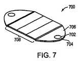
図7は、本発明に従う、2光源の導光要素700の一実施形態を示す。2光源の導光要素700は、入力結合領域702と、集積領域704と、伝搬領域706と、出力結合領域708とを有する。出力結合領域708は、示されるように正方形の形状であり得て、それにより、第1の導光要素700は、90度回転された第2の同様な導光要素700の隣にタイル状に配置されることを可能にする。このように、および以下に説明するように、第1の導光要素700の出力結合領域708は、第2の導光要素700の入力結合領域702、集積領域704および伝搬領域706の上に配置され得て、それにより、第2の導光要素のこれらの領域を隠すことになる。この様式におけるタイル状配置の結果、暗い領域のない均一な照明面を作製することとなる。しかしながら、代替の実施形態においては、出力結合領域708は矩形である。(Configuration of light guide element)
FIG. 7 illustrates one embodiment of a two light source
図8は、別の実施形態において、単一光源から光を受容するために、単一の入力結合領域802だけを有する単一光源の導光要素800を示す。単一光源の導光要素800も、集積領域804と、伝搬領域806と出力結合領域808とを含む。光は、入力結合領域802から、出力結合領域808へ、単一方向に伝搬する。2光源の導光要素700と同様に、単一光源の導光要素800を使用して平面照明領域を組み立てるには、これらを屈曲させる必要はない(出力結合領域808が隣接する要素の集積領域806を閉塞することを可能にする方式でタイル状に配置されるため)。正方形の出力結合領域808の場合、タイル状の平面照明領域の組立に必要な離散導光要素800の数は、照明面の表面の対角線の増加の二乗で増加する。(2光源の導光要素700と同様に、出力結合領域808は、多様な実施形態においては、矩形または正方形の形状である。)
本発明に従う導光要素は、図9に示されるように要素の単一側部に配設された複数の光源を有することができる。示された非対称の導光要素900は、単一の出力結合領域902と複数の隣接する入力結合904、伝搬906および集積領域908を備える縞の形状を有する。示されるように、入力結合領域は、出力結合領域902の片側部にのみ配置され、したがって、光は、2つではなく1つの側部だけから出力結合領域902に到達する。非対称の導光要素900は、任意のサイズの平面照明領域を組み立てるために使用され得る。出力結合領域902は、示されるように、通常、矩形であるが、正方形または他の任意の形状であり得る。FIG. 8 illustrates, in another embodiment, a single light source
A light guide element according to the present invention can have multiple light sources disposed on a single side of the element as shown in FIG. The asymmetric
一部の実施形態においては、導光要素は、組立時に重ね合わされずに、折り畳まれる。図10は、一実施形態において、折り畳まれた2光源2方向の導光要素1000を示す。折り畳まれた要素1000は、2光源の導光要素700の構成を有するが、2つの光源、入力結合領域1002、集積領域1004および伝搬領域1006が導光要素の出力結合領域1008の下に隠されるように、それ自体を覆って折り畳まれる。折り畳まれた2光源の導光要素1000は、正方形状の出力結合領域1008を有することができる。正方形の対称性は、折り畳まれた2光源の導光要素1000が並んでタイル状に配置することを可能にするために所望される。一実施形態においては、各折り畳まれた2光源の導光要素1000は、隣接する要素1000に対して90度回転されるため、1つの要素1000の各折り畳まれた側部が、隣接する要素1000の折り畳まれていない側部に接する。平面照明領域の組立に必要な正方形の2光源の導光要素1000の数は、その領域の対角線の増加の二乗で増加する。 In some embodiments, the light guide elements are folded without being superimposed during assembly. FIG. 10 shows a folded
図11は、折り畳まれた単一光源の二方向の導光要素1100を示す。この導光要素は、光源が1つだけであることを除き、折り畳まれた2光源の導光要素1000に類似し、入力結合領域1102が重なり合う。光源からの光は、反対方向から、すなわち、入力結合領域1102を通じて出力結合領域1104へ伝搬する。平面照明領域の組立に必要な正方形の1光源の導光要素1100の数は、その領域の対角線の増加の二乗で増加する。 FIG. 11 shows a folded single light source bi-directional
多様な実施形態においては、2光源の導光要素700、単一光源の導光要素800、非対称の導光要素900、折り畳まれた2光源の導光要素1000および/または折り畳まれた1光源導光要素1100は、機能的要件に従って、これらの特性を変更するように変形され得る。例えば、入力結合、集積および伝搬領域が出力結合領域と係合する様式は変形され得る。一実施形態においては、単一光源からの光は、2つ以上の方向から出力結合領域に結合され、それにより、より効率性の高い均一な光出力が可能になる。出力結合領域の形状を正方形または矩形のどちらかに変更する等、他の変形も行われ得る。正方形の形状は、回転対称を与え、それにより、平面照明の組立を簡素化することができるが、一方で、矩形の形状は、任意の所望のサイズの矩形平面照明の組立を促進する。加えて、導光要素の可撓性は、特定のタイル状配置または折り畳み技法に準じて調整され得て、導光要素が、隣接する導光要素の非照明領域を隠すように屈曲されることが必要になる場合がある。導光要素は、2つ以上の光源を有することもできる。導光要素のサイズは、平面照明領域を組み立てるために必要な導光要素の合計数を変更するように調整され得る。例えば、単一の平面構成は、様々なサイズまたは構成を有する要素を利用することができる。 In various embodiments, a two light source
(導光要素のタイル状配置および平面照明領域の組立)
本発明の実施形態による光を放射しない導光要素の領域は、光を放射する別の導光要素の領域により閉塞され(すなわち、後ろに隠され)得る。具体的には、入力結合、集積および/または伝搬領域は、出力結合領域の下に隠され得る。例えば、出力結合領域は、異なる導光要素上の入力結合領域に結合され得る。したがって、面を作製するために使用される導光要素の一部の領域は光を放射することがなくても、大型の均一に照明される面が構築され得る。面は、曲線形状または球形を含む多様な形状で構成され得る。(Tile arrangement of light guide elements and assembly of flat illumination area)
An area of a light guide element that does not emit light according to embodiments of the present invention may be occluded (ie, hidden behind) by an area of another light guide element that emits light. In particular, the input coupling, integration and / or propagation region may be hidden under the output coupling region. For example, the output coupling regions can be coupled to input coupling regions on different light guide elements. Thus, a large, uniformly illuminated surface can be constructed even though some areas of the light guide element used to create the surface do not emit light. The surface can be configured in a variety of shapes including a curved shape or a spherical shape.
平面照明領域は、多様な用途において実質的に均一な照明を提供するように使用され得る。一実施形態においては、平面照明領域は、点灯用途の照明器具として使用される。別の実施形態においては、平面照明領域は、例えば、液晶表示(LCD)の表示装置のバックライトユニットとして使用される。この実施形態においては、LCDは、複数のピクセルを含み、導光要素の前面に設置される。 The planar illumination area can be used to provide substantially uniform illumination in a variety of applications. In one embodiment, the planar illumination area is used as a lighting fixture for lighting applications. In another embodiment, the planar illumination area is used, for example, as a backlight unit of a liquid crystal display (LCD) display device. In this embodiment, the LCD includes a plurality of pixels and is placed in front of the light guide element.
各平面照明ユニットは、光を生成および/または転送する独立ユニットを表すことができる。平面照明領域は、各々以下に詳細を説明する、セグメント組立、ストライプ組立、タイル組立、または折り畳み構成組立等の多様な適切な組立技法のうちのいずれかにしたがって、平面照明ユニットから組み立てられ得る。 Each planar lighting unit may represent an independent unit that generates and / or transmits light. The planar illumination area may be assembled from the planar illumination unit according to any of a variety of suitable assembly techniques, such as segment assembly, stripe assembly, tile assembly, or folded component assembly, each described in detail below.
セグメント組立は、上記の導光要素の場合、各々の導光要素が表面上に表向きで単純に配置される、技法である。一部の導光要素の出力結合領域は、それまでに配置された他の導光要素の入力結合領域を覆うように配設される。一部の導光要素の場合、それまでに配置された導光要素の出力結合領域は、持ち上げられるため、新しい導光要素の入力結合領域がその下に滑り込める。この持ち上げる手順により、導光要素の少なくとも一部が持ち上げを容易にする十分な可撓性性を示すことが必要になり得る。一実施形態においては、各導光要素は、0、1、または2つの光源を隠す矩形の出力結合領域を有する。 Segment assembly is a technique where, for the light guide elements described above, each light guide element is simply placed face up on the surface. The output coupling area | region of some light guide elements is arrange | positioned so that the input coupling area | region of the other light guide element arrange | positioned so far may be covered. In the case of some light guide elements, the output coupling area of the previously arranged light guide element is lifted, so that the input coupling area of the new light guide element slides underneath. This lifting procedure may require that at least a portion of the light guide element exhibit sufficient flexibility to facilitate lifting. In one embodiment, each light guide element has a rectangular output coupling area that hides zero, one, or two light sources.
図12は、平面照明領域1200が、9つの離散導光要素1202から構築される、セグメント組立技法の実施例を示し、これは要素700(しかし、多様な実施形態においては、上記の任意の導光要素であり得る)に対応する。構造1200は、導光要素1202の正方形または矩形の出力結合領域1204のみから光を放射する。導光要素1202の入力結合、集積、および伝搬領域1206、1208、および1210は光を放射しない。 FIG. 12 shows an example of a segment assembly technique in which a
図13は、平面照明領域1200の一部1300を詳細に示す。第1の導光要素1202の入力結合領域1206は、第2の導光要素1202’の発光出力結合領域1204’の下に隠される。隣接する要素の出力結合領域1204”は、要素1202’の別の入力結合領域1206’から光を受容する。 FIG. 13 shows a
図14は、離散導光要素1402から大型の平面照明領域を構築するための別のセグメント組立技法を示す。この実施例においては、示された様式において、9つの導光要素1402は、各導光要素1402の非発光部分が隣接する導光要素1402の発光部分の後ろに隠れるように、3×3の格子1405に組み立てられる。図14に示された統合の原理は、任意のサイズ、形状および格子の数の平面照明領域に適用され得る。 FIG. 14 shows another segment assembly technique for building a large planar illumination area from discrete
図15には別の光源要素構成が示される。対称的な縞状の要素500は、各導光要素1502が、近傍の導光要素1502と光源を共有するような、導光要素1502の数珠つなぎを表す。この結果、近傍の導光要素1504の入力結合領域1504は重なり合い、縞状のN個の導光要素は、N+1個の光源だけを必要とする。しかしながら、各出力結合領域1506は、入力結合領域1504から伝搬される2方向から光を受容する。出力結合領域1506は、正方形または矩形であり得る。導光要素1502は、縞1500を備える平面照明領域を組み立てるためには屈曲される必要があり得る。平面照明領域の組立に必要な離散導光要素の数は、その領域の対角線の増加に対して線形に増加し得る。 FIG. 15 shows another light source element configuration. Symmetric striped elements 500 represent a daisy chain of
図16Aおよび16Bを参照すると、平面照明領域1600は、第1のセットの縞1500を隣接して配設してから、第2のセットの隣接する縞を第1のセットの縞を通して垂直方向に織り合わせることにより、縞1500から組み立てられ得る。上と下を織り合わせるステップは、出力結合領域1506を各入力結合領域1504およびその関連集積および伝搬領域の上に配置するために実行される。この手順によって、概して、導光要素1502が、織り合わせが発生することを可能にするある程度の可撓性を示すことが必要になる。 Referring to FIGS. 16A and 16B, the
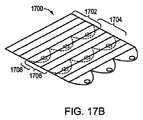
図17Aおよび17Bは、非対称の導光要素1702を使用して組み立てられた例示的な平面照明領域1700を示し、これは図9に示された要素900に対応する。第1の非対称の導光要素1702は、照明領域の終端部に配置される。第2の非対称の導光要素1704は、第2の非対称の導光要素1704の出力結合領域1706が、第1の非対称の導光要素1702の入力結合領域1708を覆うように、第1の非対称導光要素1702の隣に配置される。同一様式で他の非対称の導光要素が追加される。この組立技法では、各タイルが所望の形成因子に予め形成され得るため、要素に可撓性を要求せず、したがって、非対称導光要素1702は屈曲される必要がない。別の実施形態においては、単一光源導光要素(図8に示された要素800に対応する)は、非対称の導光要素1702に類似した一群の要素を形成するように相互に隣接して配置されてから、この一群の要素が、平面照明領域1700に対応する構造を形成するために使用される。 FIGS. 17A and 17B show an exemplary
図18は、平面照明領域1800が、隣接して単純にタイル状に配置される、折り畳まれた2光源の導光要素1802(図10に示された要素1000に対応する)から形成され得るようすを示す。平面照明領域1800は、折り畳まれた1光源の導光要素(図11に示された要素1100に対応する)からも形成され得る。折り畳まれた導光要素1802は、各折り畳まれた導光要素の出力領域がその導光要素の入力結合領域を隠すため、別の隣接する導光要素の後ろに1つの導光要素を隠す必要がない。 FIG. 18 shows that the
図19は、その出力結合領域の下に折り畳まれた入力結合、集積および伝搬領域を有する、複数光源の導光要素1902(図9に示した複数光源要素900に類似)を使用して組み立てられた平面照明領域1900を示す。1つの折り畳まれた複数光源の導光要素1902の出力結合領域は、隣接する折り畳まれた複数光源の導光要素1904の入力結合、集積および伝搬領域を隠すために使用される必要がないため、要素1902は、隣接して単純にタイル状に配置され得る。要素1902を屈曲して、平面組立体を達成する必要はない。 FIG. 19 is assembled using a multiple light source light guide element 1902 (similar to the multiple
(ステッチ)
上記のように複数の導光要素から組み立てられた平面照明領域は、タイル間の境界領域、または「ステッチ」で不均一な光を放射し得る。(stitch)
Planar illumination areas assembled from multiple light guide elements as described above may emit non-uniform light at the border areas, or “stitches” between tiles.
なぜステッチが不均一な光を放射し得るかの理由はいくつかある。例えば、不均一な光は、導光要素の構成、システムの迷光、および/または例えば、導光要素自体または組立方法に起因する導光要素の側壁の粗度または真円度による場合がある。隣接する導光要素に対して垂直に各導光要素を配置する平面照明領域の構造は、隣接するタイル間の光の進行軸の配置により、導光要素の境界において不均一性という問題を生み得る。出力結合領域におけるタイルからの発光方向は、導光板における光の進行方向に類似し得る。タイルが相互に隣に配置されると、タイル間の発光方向の非継続性により、均一性の欠落が生まれ得る。 There are several reasons why stitches can emit uneven light. For example, the non-uniform light may be due to the configuration of the light guide element, stray light of the system, and / or the roughness or roundness of the light guide element sidewalls due to, for example, the light guide element itself or the assembly method. The structure of the planar illumination area in which each light guide element is arranged perpendicular to the adjacent light guide element causes a problem of non-uniformity at the boundary of the light guide element due to the arrangement of the light traveling axis between adjacent tiles. obtain. The light emission direction from the tile in the output coupling region may be similar to the light traveling direction in the light guide plate. When tiles are placed next to each other, discontinuity in the direction of light emission between the tiles can result in a lack of uniformity.
不均一な光は、システムの迷光による場合もある。図20は、平面照明領域2000の断面図を示し、ここでは、1つの導光要素2002が、隣接する導光要素2004の表面上に置かれている。この構成では、迷光2010は、第1の導光要素の入力結合領域2008から、2つの導光要素2002、2004の間を通過してから、平面照明領域2000の外側2010に出てくることが可能になり得る。 Non-uniform light may be due to stray light in the system. FIG. 20 shows a cross-sectional view of the
加えて、図21の構造2100から分かるように、上側の導光要素2106の端部に近接する下側の導光要素2104から放射された光2102は、上側の導光要素2106の側壁2108に接触して反射され得る。光2102の本来の軌跡2110は、このように反射経路2112へと変更され得る。このように、上側の導光要素2106の側壁2108は、放射された光2102を遠くへ反射するため、その近接で不均一な光のパターンが生成し得る。 In addition, as can be seen from the
不均一な光は、導光要素の側壁の粗度および/または真円度によっても発生し得る。図22は、例えば、2つの隣接する導光要素2202、2204の側壁2206の不完全度のために、導光要素2202、2204が距離dだけ離れている構造2200を示す。導光要素2202、2204の間の隙間2208もまた、放射された光2210の分布に隙間を生成し得る。 Non-uniform light can also be generated by the roughness and / or roundness of the side walls of the light guide element. FIG. 22 shows a structure 2200 in which the
多様な実施形態においては、導光要素の慎重な配置および/または構成により、導光要素の境界で放射される不均一な光の量が削減され得る。加えて、導光要素間の境界の不明瞭さを生成して可視性を隠蔽する構造が、平面照明領域に追加され得る。 In various embodiments, careful placement and / or configuration of the light guide elements can reduce the amount of non-uniform light emitted at the boundaries of the light guide elements. In addition, structures that create ambiguity of the boundaries between the light guide elements to hide visibility may be added to the planar illumination area.
一実施形態においては、導光要素の壁は、そこから放射される光を削減するように変形され、それにより、導光要素間の境界で放射される不均一な光を削減する。例えば、導光要素の壁は、光を吸収または反射する材料で覆われ得るが、終端域から集中した光の放射を妨げない。これは、導光要素の側壁に当たる光の少なくとも一部を多方向に拡散して、光は導光の上側または下側の面から放射される。別の実施形態においては、導光の壁は、約20nm二乗平均平方根約20nmまたは全振幅150nmの公差まで研磨される。したがって、導光要素の側壁上の入射光は、拡散せずに反射または屈曲され得る。別の実施形態においては、導光要素の壁は、全振幅約600nm未満の公差まで研磨される。光が屈折する場合、光は、伝搬導光要素を通過して、近傍の導光要素に入り得て、放射または再屈折され得る。光が反射される場合、本来の導光要素中の伝搬を継続し得る。 In one embodiment, the walls of the light guide elements are deformed to reduce light emitted therefrom, thereby reducing non-uniform light emitted at the boundaries between the light guide elements. For example, the wall of the light guide element may be covered with a material that absorbs or reflects light, but does not interfere with the emission of light concentrated from the termination area. This diffuses at least part of the light impinging on the side wall of the light guide element in multiple directions, and the light is emitted from the upper or lower surface of the light guide. In another embodiment, the light guide wall is polished to a tolerance of about 20 nm root mean square about 20 nm or a total amplitude of 150 nm. Thus, incident light on the side walls of the light guide element can be reflected or bent without diffusing. In another embodiment, the light guide element walls are polished to a tolerance of less than about 600 nm total amplitude. If the light is refracted, the light can pass through the propagating light guide element and enter a neighboring light guide element, and can be emitted or re-refracted. If the light is reflected, it can continue propagation in the original light guide element.
別の実施形態においては、導光要素の側壁の形状は、光の放射に影響を与えるように変形され得る。図23は、導光要素2300の一部を示し、導光要素の側壁2304が導光要素2300の表面2306と接触する、接合2302は湾曲している。湾曲域2304は、それに当たる光2308の入射角を変更し、それにより、光2308が導光要素2300の外へ屈折することを可能にする。関連の実施形態において、側壁の一部に当たる光が、臨界入射角に対して適切な角度で当たる場合、導光要素の研磨された側壁からも光が放射され得る。 In another embodiment, the shape of the side wall of the light guide element can be modified to affect the light emission. FIG. 23 shows a portion of the
別の実施形態においては、図24に示されるように、導光要素2400の側壁2402は、導光要素2400の上側および下側の面2404、2406に対して直角を作成する。導光要素2400の側壁2402の角度は、それだけで、または側壁2402の研磨と組み合わせて、側壁2402に到達する光2408を、導光要素2400から放射されるのではなく、反射させる。 In another embodiment, as shown in FIG. 24, the
導光要素の境界から放射される不均一な光を軽減するために、分散シートが使用され得る。それにより、光は、境界に近接する導光要素の表面から広角で、かつ境界線の方向に対して横方向に放射される。この様式に放射する2つの導光要素を結合すると、例えば、10〜20%の拡散方向伝達および80〜70%の逆方向伝達等の小さい拡散値を有する透明な拡散シートの助けを借りて、境界線の可視性が不明瞭化する。 A dispersion sheet can be used to mitigate uneven light emitted from the boundaries of the light guide elements. Thereby, light is emitted at a wide angle from the surface of the light guide element adjacent to the boundary and in a direction transverse to the direction of the boundary line. Combining two light guide elements radiating in this manner, for example, with the help of a transparent diffusion sheet with a small diffusion value, such as 10-20% diffusion direction transmission and 80-70% reverse transmission, The visibility of the boundary line is obscured.
例えば、図25に示されるように、平面照明領域2500は、透明な拡散シートにより覆われ得る。この実施例においては、各導光要素2502は、サイズが82mm×63mmで、近傍の導光要素から6mm離れている。照明面から拡散板までの最大距離は4.5mmである。図26の黒い三角形の中心のステッチの不均一性は、以下の数式を使用してシミュレートされ得る。 For example, as shown in FIG. 25, the

広角での光の放射は、1つの軸に沿って共に接合され、垂直軸に沿って相互を覆って置かれる導光要素間の境界線の不明瞭化を可能にし得る。光は、導光要素の間の境界線に対して垂直方向で広角に、および境界線と平行方向に狭角に放射され得て、拡散シートは、導光要素を覆って配置され得る。この構造は、照明面の輝度を増加し、例えば、輝度強化フィルム(「BEF」)シートが放射される光の角度を削減し、より高い輝度を取得するために使用される、バックライトユニット(BLU)用途で有用であり得る。2つの軸の光の放射角の範囲においては、対称性が欠落し得る。BLU用途の場合、対称性の欠落は、水平軸の方向に広角の光を、かつ縦軸の方向に狭角の光を放射する場合に適し得る。一実施形態においては、図26に示されるように、BLU2200は、水平軸2604の方向に互いに近接してタイル状に配置され、垂直軸2606方向に一枚一枚重ねられた導光要素2602を含む。別の実施形態においては、導光要素2602の光の伝搬方向は、別の整合された導光要素に対して連続的で、それにより、光の伝搬方向における結合が削減される。 The emission of light at a wide angle may allow obscuration of the boundaries between light guide elements that are joined together along one axis and placed over each other along a vertical axis. The light can be emitted at a wide angle in a direction perpendicular to the boundary line between the light guide elements and at a narrow angle in a direction parallel to the boundary line, and the diffusion sheet can be disposed over the light guide element. This structure increases the brightness of the illumination surface, for example, reduces the angle of light emitted by a brightness enhancement film (“BEF”) sheet, and is used to obtain higher brightness backlight units ( BLU) applications may be useful. Symmetry may be lost in the range of the light emission angles of the two axes. For BLU applications, the lack of symmetry may be suitable when emitting wide angle light in the horizontal axis direction and narrow angle light in the vertical axis direction. In one embodiment, as shown in FIG. 26, the BLU 2200 includes
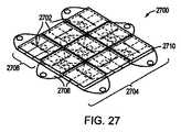
別の実施形態においては、図27に示されるように、複合構造2700を形成するように、平面照明領域2704の上に設置される、BEFシート等の光学プリズムシート2702を適切に配設することにより、光の方向の結合がバランスされ得る。光学プリズムシート2702の方向は、概して、導光要素2706の光の伝搬方向に整合され、各光学プリズムシート2702は、隙間2710により分離される、導光要素2706の出力結合領域2708の上に置かれる。 In another embodiment, as shown in FIG. 27, an
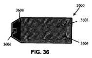
図28に示された構造2800を参照すると、光吸収面2802は、図20を参照して説明したように、2つの導光要素2806、2808がその間から逃げる光の量を削減するように重なり合う、領域2804に設置され得る。光吸収面2802は、結合されて内部で拡散することを可能にすることにより、この光の出口角を削減する、あるいは光を屈折して導光要素2806、2808に戻す、BEFシート等のプリズム光学フォイルであり得る。このようにして、光は、導光要素2806、2808に拡散する光に合流するように再利用され得る。迷光が導光要素2806、2808の垂直方向に対して鈍角である場合、光吸収要素2802により回収され得る光が多くなる。 Referring to the
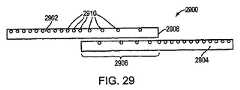
隣接する導光要素は重なり合い得て、導光要素の照明の間の著しい対照を削減する。図29は、構造2900を示し、第1の導光要素2902は、隣接する導光要素2904の上に置かれている。上側の導光要素2902の光の放射域は、下側の導光要素2904の入力結合、集積および伝搬領域だけでなく、その出力結合領域の一部も覆う。この構成によって、導光要素2902、2904の間の遷移または重複領域2906の作成が可能になる。一実施例においては、上側の導光要素2902の端部2908は、非直線を形成する。光は、下側の導光要素2904の出力結合領域から、上側の導光要素2902を通って放射されて、導光要素2902、2904の間の遷移域2906全体で光の強度に緩やかな変化を作成する。この緩やかな変化は、遷移領域2906の導光要素2902、2904の各々の光散乱要素2910(例えば、上記の粒子)の密度を段階的に減少させることにより作成され得る。図30は、導光要素2902、2904の各々の出力が遷移区域2906でどのように減少するかを示す。しかしながら、両方の導光要素2902、2904の出力の和3000は、遷移区域2906の領域全体でほぼ一定(すなわち、均一)でなければならない。一実施形態においては、遷移領域2906と導光要素2902、2904の非重複出力結合領域との間の出力は、実質的に均一、すなわち、10%以内の差である。 Adjacent light guide elements can overlap to reduce significant contrast during illumination of the light guide elements. FIG. 29 shows a
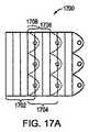
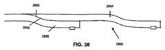
図31には、重複する導光要素3102から作成された別の平面照明領域3100が示される。この実施形態においては、導光要素3102は、一方向3104に段階的方式でタイル状に配置され、他の方向3106には緊密に配置される。図32Aおよび32Bは、それぞれ、構造3100において使用され得る導光要素3204の上面図および底面図3200、3202を示し、図33は側面図3300を示す。遷移領域3206は、出力結合領域3208の両側に存在する。各導光要素3204は、底面反射体3210と、光源3212と、透明領域3214とも備える。この構成においては、要素の出力結合領域が別の要素の出力結合領域の下にある場合、上に重なっている出力結合領域から放射される光を集めないように、透明である。 FIG. 31 shows another
図34に示される、別の実施形態においては、平面照明領域3400は、一連の導光要素3402を2方向3404、3406に重ね合わせることにより作成され得る。図35および36を参照すると、遷移領域3502は、導光要素3508の上面図3500および底面図3600により示されるように、その4つ全ての側部上の出力結合領域3504を包囲し、他の4つのタイルが、遷移領域3502の4つ全ての側部と重なり合う、または重ね合わされることを可能にする。出力結合領域3504、光源3506、底面反射体3602および透明領域3604も示される。遷移領域3502は、例えば、隣接するタイルの繊維領域の特徴に応じて、2つまたは4つの側部が透明であり得る。ここでも、目的は、重複領域で一定の光出力を保持することである。 In another embodiment, shown in FIG. 34, a
第1の導光要素の側壁は、第1の導光要素と第2との重なり合いが、形成される平面照明領域の高さで均一性を欠落させないように、形成され得る。例えば、図37の平面照明領域3700に関して示されるように、第1の導光要素3704の第1の側壁3702は、非垂直方向であり得て、隣接の第2の導光要素3708の第2の側壁3706は、非垂直方向で、かつ第1の側壁3706を補完し得る。2つの導光要素3704、3708は、平面照明領域3700の高さhが変化することなく、非垂直方向の側壁3702、3706を含む領域3710において重なり合う。図38に示された代替の実施形態3800においては、第1の導光要素3804の側壁3802は、隣接する、第2の導光要素3808の曲面3806に適合するように湾曲し得る。 The side walls of the first light guide element may be formed such that the overlap of the first light guide element and the second does not lose uniformity at the height of the planar illumination area to be formed. For example, as shown with respect to the planar illumination region 3700 of FIG. 37, the
図39A〜Bは、代替の実施形態において、透明な充填材料3904を含む2つの平面照明領域3900、3902の側面図である。平面照明領域3900は、透明な充填材料3904を使用して、導光要素3906を重ね合わせることにより作成される域3900の高さにおける不規則性を削減する。透明な充填材料3904の屈折率は、導光要素3906の屈折率に一致することが好ましい。加えて、透明な充填材料3904を使用すると、平坦で円滑な照明面3908が作成される。代替の実施形態においては、平面照明領域3902は、導光要素3906間の空間に透明な充填材料3904を含み、この透明な充填材料3904は、導光要素3906の屈折率に一致する屈折率を有することが好ましい。 FIGS. 39A-B are side views of two
研磨された壁を備えるタイル構造を、上記のように、平面照明領域3902と共に利用すると、各導光要素とその近傍との間に継続性が生成されるようになり得て、光が近傍のタイル間で拡散することを可能にする。近傍のタイル間の光を集約すると、上記のような重ね合わせる構造を必要とせずに、所望に応じて、ステッチ線の2つの側部間の光強度に連続かつ単調な変化が生成される。 When a tile structure with polished walls is utilized with a planar illumination area 3902 as described above, continuity can be generated between each light guide element and its vicinity, so that light is in the vicinity. Allows diffusion between tiles. Aggregating light between neighboring tiles produces a continuous and monotonic change in the light intensity between the two sides of the stitch line, as desired, without the need for overlapping structures as described above.
(LEDサブアセンブリ)
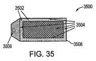
本発明の多様な実施形態においては、LEDサブアセンブリが導光要素に付設される。LEDサブアセンブリは、少なくとも1つの光源のためのプラットフォームとして機能し、導光要素への電気的および機械的接続性を提供する。図40は、キャリアプラットフォーム4002、LEDベアダイチップ4004、プリント基板(「PCB」)4006、およびインターフェースボード4008を含む、LEDサブアセンブリ4000の例示的な実施形態を示す。これらの構成要素は図41〜44に詳細が示される。他の実施形態においては、LEDベアダイチップ4004は、パッケージ化されたLED、RGBまたは白色光源で置換され得る。光源は、サイド放射または最上部放射型(すなわち、ランベルト)光源のいずれかであり得る。(LED subassembly)
In various embodiments of the present invention, an LED subassembly is attached to the light guide element. The LED subassembly serves as a platform for at least one light source and provides electrical and mechanical connectivity to the light guide element. FIG. 40 illustrates an exemplary embodiment of an
図41は、1つ以上の光源をサポートするために適切なキャリアプラットフォーム4002を含む構造4100を示す。光源は、例えば、ベアダイLEDチップ4004であり得る。キャリアプラットフォーム4002は、LEDのアセンブリに使用される任意のプラットフォームであり得て、一部の実施形態においては、優れた熱伝導性を示す。キャリアプラットフォーム4002は、LEDベアダイチップ4004を機械的にサポートし得て、熱伝導によりLEDベアダイチップ4004からの熱消散を可能にし、かつLEDベアダイチップ4004への電気的接続を提供する。 FIG. 41 shows a
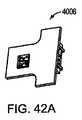
図42Aおよび42Bは、一実施形態において、それぞれ、プリント基板4006の上面および底面の図を示す。LEDベアダイチップ4004を備えるキャリアプラットフォーム4002は、接続体を介して、プリント基板4006上に取り付けられ得る。プリント基板4006は、光源に電流を提供する輪郭電気接続を含む。プリント基板4006は、キャリアプラットフォーム4002を機械的にもサポートし、熱的に接触状態にあり、したがって、光源からの熱消散を向上させる。 42A and 42B show top and bottom views of a printed
図43は、機械的接続性および照明源へのサポートを提供する、インターフェースボード4008の一実施形態を示す。インターフェースボードは、LEDサブアセンブリ4000全体を導光要素に機械的に接続する。さらに、必要な用途構造への平面照明源の機械的接続を可能にし得る。また、平面照明源と用途構造との間に熱接続を提供することにより熱消散も支援する。 FIG. 43 illustrates one embodiment of an
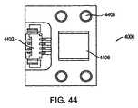
図44は、LEDサブアセンブリ4000の底面図を示し、電気インターフェース4402、機械インターフェース4404、および熱伝導インターフェース4406が確認できる。図45は、平面照明源4500を形成するように、導光要素4502と共に組み立てられたLEDサブアセンブリ4000を示す。LEDベアダイチップ4004は、キャリアプラットフォーム4002上に取り付けられ、LEDサブアセンブリ4000と導光要素4502の入力結合領域4504とを接合することにより形成される適切なソケットに設置され得る。LEDベアダイチップ4004から放射される光は、導光要素4502の入力結合領域4504に結合される。 FIG. 44 shows a bottom view of the
一実施形態においては、LEDベアダイチップ4004は、LEDサブアセンブリ4000に設置され、これは、導光要素のポリマーを破損する可能性がある高温(例えば、約85℃より高温)が必要な他の組立手順後に、後で導光要素4502に付設される。導光要素4502の入力結合領域4504とキャリアプラットフォーム4002との間のあらゆる隙間は、適切な充填材料で充填され得る。充填材料は、LEDの動作温度(例えば、約150℃未満または約70℃未満でも)に耐えることができるが、LEDサブアセンブリ4000の組み立て(例えば、約250℃のハンダ付け)に必要なこれより高い温度には耐えることができない。充填材料は、概して、LEDソケットを充填し、LEDダイの表面およびそれに接続されるいずれのワイヤ接合をも覆う。適切な充填材料の実施例は、Dymax Corporation(Torrington、CT)から販売されているLIGHT WELD9620等のUV硬化性接着剤、およびNuSil Technology LLC(Wareham、MA)から販売されているLS−3249およびLS−3252等のカプセルジェルを含む。LEDベアダイチップ4004は、適切な光学および機械的特徴を備える中間材料を使用して、導光要素4502に直接結合され得る。この中間材料は、LEDベアダイチップ4004を覆って配置されるカプセル構造の全てまたは一部であり得る。カプセルの形状は、導光要素4502との光学インターフェースの形状および屈折率の要件によって決められる。カプセル要素が使用される場合、導光要素4502のソケットの壁とカプセル構造の外表面との間の空間は、適切な光学および機械的特徴を備える光学接着材で充填され得る。 In one embodiment, the LED
本明細書に採用された用語および表現は、限定ではなく、説明の用語および表現として使用されるものであり、このような用語および表現の使用においては、表示および説明された特徴の任意の相当物またはその一部を排除する意図は存在しない。加えて、本発明の所与の実施形態を説明したが、当業者には、本発明の精神および範囲を逸脱することなく、本明細書で開示された概念を組み入れる他の実施形態が使用され得ることが明らかであろう。したがって、説明された実施形態は、あらゆる点において、図示であって限定ではないと見なされたい。 The terms and expressions employed herein are to be used as descriptive terms and expressions, and not as limitations, and in the use of such terms and expressions, any equivalent of the features shown and described There is no intent to exclude things or parts thereof. In addition, while a given embodiment of the present invention has been described, those skilled in the art will recognize other embodiments that incorporate the concepts disclosed herein without departing from the spirit and scope of the present invention. It will be clear to get. Accordingly, the described embodiments are to be considered in all respects only as illustrative and not restrictive.
Claims (90)
Translated fromJapanese第1の入力結合領域と、そこから空間的に分離された第1の出力結合領域とを含む、第1の導光要素を提供することであって、それにより、該第1の入力結合領域に入射する光は、該第1の出力結合領域からの放射のために、該第1の導光要素内で実質的に保持される、ことと、
重複領域を形成するように、第2の導光要素の一部を該第1の導光要素の一部の上に重ね合わせることであって、該第2の導光要素は、第2の入力結合領域と、そこから空間的に分離された第2の出力結合領域とを備え、それにより、該第2の入力結合領域に入射する光は、該第2の出力結合領域からの放射のために、該第2の導光要素内で実質的に保持される、ことと
を含み、該重複領域は、少なくとも、該第1の入力結合領域と、該第1の入力結合領域を完全に閉塞する該第2の出力結合領域の少なくとも一部とを含む、方法。A method of forming a planar light emitting surface from a plurality of light guide elements, the method comprising:
Providing a first light guide element comprising a first input coupling region and a first output coupling region spatially separated therefrom, whereby the first input coupling region Light incident on the first light guide element is substantially retained in the first light guide element for radiation from the first output coupling region;
Overlaying a portion of the second light guide element on a portion of the first light guide element to form an overlapping region, wherein the second light guide element is a second An input coupling region and a second output coupling region spatially separated therefrom, so that light incident on the second input coupling region is free of radiation from the second output coupling region; The overlap region is at least completely connected to the first input coupling region and the first input coupling region. And at least a portion of the second output coupling region that occludes.
該第2の重複領域は、該第3の出力結合領域の少なくとも一部を含む、
請求項13に記載の方法。Overlaying at least a portion of the third light guide element on at least a portion of the second light guide element to form a second overlap region, the third light guide element Includes a third input coupling region and a third output coupling region spatially separated therefrom so that light incident on the third input coupling region is coupled to the third output coupling region. Further retained substantially within the third light guide element for radiation from a region;
The second overlapping region includes at least a portion of the third output coupling region;
The method of claim 13.
出力結合領域が全入力結合領域を閉塞するように、各追加の導光要素の一部を隣接する導光要素の一部の上に重なり合わせることと
を含む、請求項13に記載の方法。Providing additional light guide elements, each including an input coupling region and an output coupling region spatially separated therefrom, so that light incident on the input coupling region is coupled to the output coupling region Substantially retained within the corresponding light guide element for radiation from a region;
14. The method of claim 13, comprising overlapping a portion of each additional light guide element over a portion of an adjacent light guide element such that the output coupling region occludes the entire input coupling region.
第1の入力結合領域と、第1の出力結合領域とを含む、第1の導光要素を提供することであって、該第1の入力結合領域および該第1の出力結合領域は、空間的に別個であり、それにより、該第1の入力結合領域に入射する光は、該第1の出力結合領域からの放射のために、該導光要素内に保持される、ことと、
該第1の導光要素に隣接する第2の導光要素を提供することであって、該第2の導光要素は、第2の入力結合領域と、第2の出力結合領域とを含み、該第2の入力結合領域および該第2の出力結合領域は、空間的に別個であり、それにより、該第2の入力結合領域に入射する光は、該第2の出力結合領域からの放射のために、該導光要素内で保持される、ことと
を含み、該隣接する第1および第2の導光要素が、光の連続面を放射するように、該第1の出力結合領域は、該第1の入力結合領域を閉塞し、該第2の出力結合領域は、該第2の入力結合領域を閉塞する、方法。A method of forming a planar light emitting surface from a plurality of light guide elements, the method comprising:
Providing a first light guide element that includes a first input coupling region and a first output coupling region, wherein the first input coupling region and the first output coupling region are spaces. Separate, whereby light incident on the first input coupling region is retained in the light guide element for radiation from the first output coupling region;
Providing a second light guide element adjacent to the first light guide element, wherein the second light guide element includes a second input coupling region and a second output coupling region. , The second input coupling region and the second output coupling region are spatially separate, so that light incident on the second input coupling region is from the second output coupling region The first output coupling such that the adjacent first and second light guide elements emit a continuous surface of light. A region occludes the first input coupling region and the second output coupling region occludes the second input coupling region.
サブアセンブリプラットフォームの凹部の中に離散光源を提供することと、
該サブアセンブリプラットフォームを導光要素に接合し、それにより、該離散光源が配置される、閉鎖型ソケットを形成することとを含む、方法。A method of forming a lighting device, the method comprising:
Providing a discrete light source in the recess of the subassembly platform;
Joining the subassembly platform to a light guide element, thereby forming a closed socket in which the discrete light sources are disposed.
光源からの多方向光を受容するための入力結合領域と、
該導光要素から光を放射するための出力結合領域と、
該出力結合領域と反対側の該入力結合領域に近接する集積領域であって、該集積領域は、該入力結合領域からの多方向光を該出力結合領域に向かって方向付ける、集積領域と
を含む、導光要素。A light guide element,
An input coupling region for receiving multidirectional light from the light source;
An output coupling region for emitting light from the light guide element;
An integration region proximate to the input coupling region opposite the output coupling region, wherein the integration region directs multidirectional light from the input coupling region toward the output coupling region; Including a light guide element.
第1の出力結合領域を含む、第1の導光要素と、
第2の出力結合領域を含む、第2の導光要素であって、該第2の出力結合領域の少なくとも一部は、該第1の出力結合の少なくとも一部と重なり合って、ある領域を有する重複領域を画定する、第2の導光要素と
を備え、該重複領域は、該領域上で実質的に均一な光出力を放射する、平面照明領域。A planar illumination area,
A first light guide element including a first output coupling region;
A second light guide element including a second output coupling region, wherein at least a portion of the second output coupling region overlaps at least a portion of the first output coupling region and has a region A planar illumination region comprising: a second light guide element defining an overlap region, wherein the overlap region emits a substantially uniform light output over the region.
第1の出力結合領域を含む、第1の導光要素を提供することと、
該第1の導光要素の少なくとも一部を、第2の出力結合領域を含む第2の導光要素と重ね合わせることであって、それにより、該第1の出力結合領域の少なくとも一部と、該第2の出力結合領域とを含む、重複領域を形成する、ことと
を含み、該重複領域は、実質的に均一な光出力を放射する、方法。A method of forming a planar illumination region, the method comprising:
Providing a first light guide element including a first output coupling region;
Overlaying at least a portion of the first light guide element with a second light guide element including a second output coupling region, thereby providing at least a portion of the first output coupling region; Forming an overlapping region comprising: the second output coupling region, wherein the overlapping region emits a substantially uniform light output.
第1の側壁を備える、第1の導光要素と、
第2の側壁を備える、第2の導光要素と、
該第1および第2の側壁を覆う、屈折率整合材料であって、該屈折率整合材料の屈折率は、該第1の導光要素または該第2の導光要素のうちの少なくとも1つの屈折率にほぼ等しい、屈折率整合材料と
を備える、平面照明領域。A planar illumination area,
A first light guide element comprising a first sidewall;
A second light guide element comprising a second sidewall;
An index matching material covering the first and second sidewalls, the index matching material having an index of refraction that is at least one of the first light guide element or the second light guide element A planar illumination region comprising: a refractive index matching material that is approximately equal to the refractive index.
第1の研磨された側壁を備える、第1の導光要素と、
第2の研磨された側壁を備える、第2の導光要素であって、該第2の研磨された側壁は、該第1の研磨された側壁に隣接する、第2の導光要素と
を備え、該第2の導光要素は、該第1の研磨された側壁および該第2の研磨された側壁を通して、該第1の導光要素から光を受容する、平面照明領域。A planar illumination area,
A first light guide element comprising a first polished sidewall;
A second light guide element comprising a second polished side wall, the second polished side wall adjacent to the first polished side wall; and A planar illumination region, wherein the second light guide element receives light from the first light guide element through the first polished sidewall and the second polished sidewall.
Applications Claiming Priority (8)
| Application Number | Priority Date | Filing Date | Title |
|---|---|---|---|
| US611007P | 2007-12-19 | 2007-12-19 | |
| US6438408P | 2008-03-03 | 2008-03-03 | |
| US12709508P | 2008-05-09 | 2008-05-09 | |
| US5993208P | 2008-06-09 | 2008-06-09 | |
| US12/324,540US8172447B2 (en) | 2007-12-19 | 2008-11-26 | Discrete lighting elements and planar assembly thereof |
| US12/324,544US8550684B2 (en) | 2007-12-19 | 2008-11-26 | Waveguide-based packaging structures and methods for discrete lighting elements |
| US12/324,555US7907804B2 (en) | 2007-12-19 | 2008-11-26 | Elimination of stitch artifacts in a planar illumination area |
| PCT/IL2008/001553WO2009078007A2 (en) | 2007-12-19 | 2008-11-27 | Discrete lighting elements and planar assembly thereof |
Publications (1)
| Publication Number | Publication Date |
|---|---|
| JP2011508373Atrue JP2011508373A (en) | 2011-03-10 |
Family
ID=40788386
Family Applications (1)
| Application Number | Title | Priority Date | Filing Date |
|---|---|---|---|
| JP2010539043AWithdrawnJP2011508373A (en) | 2007-12-19 | 2008-11-27 | Discrete light emitting element and planar assembly thereof |
Country Status (2)
| Country | Link |
|---|---|
| US (5) | US7907804B2 (en) |
| JP (1) | JP2011508373A (en) |
Cited By (6)
| Publication number | Priority date | Publication date | Assignee | Title |
|---|---|---|---|---|
| JP2012234777A (en)* | 2011-05-09 | 2012-11-29 | Canon Inc | Backlight device and display device |
| WO2015030037A1 (en)* | 2013-08-28 | 2015-03-05 | 富士フイルム株式会社 | Light guide plate, backlight unit comprising same, liquid crystal display device and optical sheet |
| US9857519B2 (en) | 2012-07-03 | 2018-01-02 | Oree Advanced Illumination Solutions Ltd. | Planar remote phosphor illumination apparatus |
| US11079096B2 (en) | 2018-05-31 | 2021-08-03 | Nichia Corporation | Lighting fixture and lighting apparatus |
| JP2021519202A (en)* | 2018-03-27 | 2021-08-10 | コーニンクレッカ フィリップス エヌ ヴェKoninklijke Philips N.V. | Flat biofouling prevention system using UV-C |
| JP7464264B2 (en) | 2020-04-08 | 2024-04-09 | 株式会社オオサカネーム | Strip-shaped substrate and strip-shaped LED light-emitting device |
Families Citing this family (75)
| Publication number | Priority date | Publication date | Assignee | Title |
|---|---|---|---|---|
| WO2004053531A2 (en)* | 2002-12-09 | 2004-06-24 | Oree, Advanced Illumination Solutions Inc. | Flexible optical device |
| WO2006131924A2 (en) | 2005-06-07 | 2006-12-14 | Oree, Advanced Illumination Solutions Inc. | Illumination apparatus |
| US8215815B2 (en) | 2005-06-07 | 2012-07-10 | Oree, Inc. | Illumination apparatus and methods of forming the same |
| US8272758B2 (en) | 2005-06-07 | 2012-09-25 | Oree, Inc. | Illumination apparatus and methods of forming the same |
| KR101548025B1 (en)* | 2007-07-27 | 2015-08-27 | 아사히 가라스 가부시키가이샤 | Translucent substrate, method for manufacturing the translucent substrate, organic led element and method for manufacturing the organic led element |
| US7907804B2 (en) | 2007-12-19 | 2011-03-15 | Oree, Inc. | Elimination of stitch artifacts in a planar illumination area |
| US8182128B2 (en)* | 2007-12-19 | 2012-05-22 | Oree, Inc. | Planar white illumination apparatus |
| US20100296270A1 (en)* | 2008-01-25 | 2010-11-25 | Showa Denko K.K. | Display device and light emitting device |
| US20090225566A1 (en) | 2008-03-05 | 2009-09-10 | Micha Zimmermann | Illumination apparatus and methods of forming the same |
| US8301002B2 (en) | 2008-07-10 | 2012-10-30 | Oree, Inc. | Slim waveguide coupling apparatus and method |
| US8297786B2 (en)* | 2008-07-10 | 2012-10-30 | Oree, Inc. | Slim waveguide coupling apparatus and method |
| US8462292B2 (en)* | 2008-07-31 | 2013-06-11 | Rambus Delaware Llc | Optically transmissive substrates and light emitting assemblies and methods of making same, and methods of displaying images using the optically transmissive substrates and light emitting assemblies |
| US8223296B2 (en)* | 2008-08-25 | 2012-07-17 | Lg Display Co. Ltd. | Backlight unit and liquid crystal display device having the same |
| CN102245959A (en)* | 2008-12-09 | 2011-11-16 | 夏普株式会社 | Light source unit, illuminating device, display device and television receiver |
| US20100208469A1 (en)* | 2009-02-10 | 2010-08-19 | Yosi Shani | Illumination surfaces with reduced linear artifacts |
| JP5143770B2 (en)* | 2009-03-02 | 2013-02-13 | 株式会社ジャパンディスプレイイースト | Liquid crystal display |
| US8624527B1 (en) | 2009-03-27 | 2014-01-07 | Oree, Inc. | Independently controllable illumination device |
| US20100320904A1 (en)* | 2009-05-13 | 2010-12-23 | Oree Inc. | LED-Based Replacement Lamps for Incandescent Fixtures |
| EP2440839A1 (en)* | 2009-06-11 | 2012-04-18 | Koninklijke Philips Electronics N.V. | Illumination apparatus |
| WO2010150202A2 (en) | 2009-06-24 | 2010-12-29 | Oree, Advanced Illumination Solutions Inc. | Illumination apparatus with high conversion efficiency and methods of forming the same |
| JP2011040279A (en)* | 2009-08-11 | 2011-02-24 | Sony Corp | Planar lighting device |
| KR101047601B1 (en)* | 2009-08-26 | 2011-07-07 | 엘지이노텍 주식회사 | Backlight unit and display device using same |
| WO2011033428A2 (en)* | 2009-09-16 | 2011-03-24 | Koninklijke Philips Electronics N.V. | Optical element |
| JP5401247B2 (en)* | 2009-10-02 | 2014-01-29 | 日立コンシューマエレクトロニクス株式会社 | Backlight unit and video display device using the same |
| JP2013508932A (en)* | 2009-10-27 | 2013-03-07 | コーニンクレッカ フィリップス エレクトロニクス エヌ ヴィ | Light guide for lighting systems and for scanning backlight systems |
| KR20110048173A (en)* | 2009-11-02 | 2011-05-11 | 삼성전자주식회사 | Backlight unit and display device having same |
| TW201120522A (en)* | 2009-12-02 | 2011-06-16 | Dynascan Technology Corp | Stack combinational backlight panel used in display and display having the same. |
| EP2336812A1 (en)* | 2009-12-17 | 2011-06-22 | The Swatch Group Research and Development Ltd. | Device for collimation, homogenisation and extraction of light for lighting a display device |
| WO2011115351A1 (en)* | 2010-03-15 | 2011-09-22 | Lg Electronics Inc. | Backlight unit and display apparatus including the same |
| GB2478986B (en)* | 2010-03-26 | 2015-07-01 | Iti Scotland Ltd | LED arrays |
| GB2478987A (en) | 2010-03-26 | 2011-09-28 | Iti Scotland Ltd | Encapsulation of an LED array forming a light concentrator for use with edge-lit light-guided back lights |
| JP5482588B2 (en)* | 2010-09-10 | 2014-05-07 | 富士通株式会社 | Mobile terminal device |
| CN102410498B (en)* | 2010-09-23 | 2013-04-24 | 展晶科技(深圳)有限公司 | Light-emitting diode (LED) backlight module and light guide plate thereof |
| TWI471504B (en)* | 2010-10-27 | 2015-02-01 | Young Lighting Technology Corp | Flat light source module |
| WO2012077534A1 (en)* | 2010-12-06 | 2012-06-14 | シャープ株式会社 | Lighting device and liquid crystal display device provided with same |
| US8646953B2 (en)* | 2011-01-11 | 2014-02-11 | Nittoh Kogaku K.K. | Light guiding body and light emitting device |
| JP6228110B2 (en) | 2011-04-28 | 2017-11-08 | エル イー エス エス・リミテッド | Waveguide device for illumination system |
| US8632236B2 (en)* | 2011-11-04 | 2014-01-21 | GE Lighting Solutions, LLC | LED lighting module and lighting device comprised thereof |
| US8591072B2 (en) | 2011-11-16 | 2013-11-26 | Oree, Inc. | Illumination apparatus confining light by total internal reflection and methods of forming the same |
| KR101851616B1 (en)* | 2012-01-18 | 2018-04-25 | 한국전자통신연구원 | Display |
| US8907362B2 (en) | 2012-01-24 | 2014-12-09 | Cooledge Lighting Inc. | Light-emitting dies incorporating wavelength-conversion materials and related methods |
| US8896010B2 (en) | 2012-01-24 | 2014-11-25 | Cooledge Lighting Inc. | Wafer-level flip chip device packages and related methods |
| WO2013112435A1 (en) | 2012-01-24 | 2013-08-01 | Cooledge Lighting Inc. | Light - emitting devices having discrete phosphor chips and fabrication methods |
| US20150062963A1 (en)* | 2012-03-31 | 2015-03-05 | Noam Meir | Illumination system and method for backlighting |
| US10174906B2 (en) | 2012-06-18 | 2019-01-08 | Fresnel Technologies Inc. | LED luminaire tiling with a lens array containing a plurality of lenslets |
| US9519095B2 (en) | 2013-01-30 | 2016-12-13 | Cree, Inc. | Optical waveguides |
| US9366396B2 (en) | 2013-01-30 | 2016-06-14 | Cree, Inc. | Optical waveguide and lamp including same |
| US9690029B2 (en) | 2013-01-30 | 2017-06-27 | Cree, Inc. | Optical waveguides and luminaires incorporating same |
| US9291320B2 (en) | 2013-01-30 | 2016-03-22 | Cree, Inc. | Consolidated troffer |
| US9442243B2 (en) | 2013-01-30 | 2016-09-13 | Cree, Inc. | Waveguide bodies including redirection features and methods of producing same |
| US9625638B2 (en) | 2013-03-15 | 2017-04-18 | Cree, Inc. | Optical waveguide body |
| US9869432B2 (en) | 2013-01-30 | 2018-01-16 | Cree, Inc. | Luminaires using waveguide bodies and optical elements |
| US9773760B2 (en)* | 2013-01-30 | 2017-09-26 | Cree, Inc. | LED packages and luminaires incorporating same |
| US10436970B2 (en) | 2013-03-15 | 2019-10-08 | Ideal Industries Lighting Llc | Shaped optical waveguide bodies |
| US10209429B2 (en) | 2013-03-15 | 2019-02-19 | Cree, Inc. | Luminaire with selectable luminous intensity pattern |
| US10502899B2 (en)* | 2013-03-15 | 2019-12-10 | Ideal Industries Lighting Llc | Outdoor and/or enclosed structure LED luminaire |
| US9798072B2 (en) | 2013-03-15 | 2017-10-24 | Cree, Inc. | Optical element and method of forming an optical element |
| US10379278B2 (en)* | 2013-03-15 | 2019-08-13 | Ideal Industries Lighting Llc | Outdoor and/or enclosed structure LED luminaire outdoor and/or enclosed structure LED luminaire having outward illumination |
| US10400984B2 (en) | 2013-03-15 | 2019-09-03 | Cree, Inc. | LED light fixture and unitary optic member therefor |
| US9366799B2 (en) | 2013-03-15 | 2016-06-14 | Cree, Inc. | Optical waveguide bodies and luminaires utilizing same |
| US9920901B2 (en) | 2013-03-15 | 2018-03-20 | Cree, Inc. | LED lensing arrangement |
| WO2015056220A1 (en) | 2013-10-18 | 2015-04-23 | Tissot Yann | Holder and systems for waveguide-based illumination |
| US9343443B2 (en) | 2014-02-05 | 2016-05-17 | Cooledge Lighting, Inc. | Light-emitting dies incorporating wavelength-conversion materials and related methods |
| KR20150110847A (en)* | 2014-03-20 | 2015-10-05 | 삼성디스플레이 주식회사 | Quantum dot filling tube and display device having the same |
| JP6628889B2 (en)* | 2016-02-09 | 2020-01-15 | ナノコンプ オイ リミテッド | Lightguide with multiple optical channels |
| US11719882B2 (en) | 2016-05-06 | 2023-08-08 | Ideal Industries Lighting Llc | Waveguide-based light sources with dynamic beam shaping |
| US10416377B2 (en) | 2016-05-06 | 2019-09-17 | Cree, Inc. | Luminaire with controllable light emission |
| WO2019052294A1 (en) | 2017-09-12 | 2019-03-21 | Nanoleaf Energy Technology Shenzhen Limited | Systems and methods for providing coupled lighting panels |
| CN109099343A (en)* | 2017-09-12 | 2018-12-28 | 绿诺能源科技(深圳)有限公司 | For providing the system and method for the illumination panel of connection |
| US20190192879A1 (en)* | 2017-12-22 | 2019-06-27 | Inikoa Medical, Inc. | Disinfecting Methods and Apparatus |
| US10788617B2 (en) | 2018-01-19 | 2020-09-29 | HeatchCo LLC | Outside light with diffusing light panel |
| US10683985B2 (en) | 2018-01-19 | 2020-06-16 | Heathco Llc | Security light with diffusing light panel |
| EP3750001A1 (en)* | 2018-03-07 | 2020-12-16 | Nokia Technologies Oy | An apparatus for use in a near eye display |
| CN208901150U (en)* | 2018-10-29 | 2019-05-24 | 广州启上设计有限公司 | A kind of side entering type optical lens light source and desk lamp |
| KR102732895B1 (en)* | 2018-11-26 | 2024-11-25 | 삼성전자주식회사 | Biometric sensor module and electronic device including the same |
Family Cites Families (309)
| Publication number | Priority date | Publication date | Assignee | Title |
|---|---|---|---|---|
| US640813A (en)* | 1899-03-13 | 1900-01-09 | Ernst B Schneider | Stapling-machine. |
| GB512062A (en) | 1938-01-28 | 1939-08-29 | Ernst Hirsch | Improvements in reflectors |
| US3261356A (en) | 1963-10-21 | 1966-07-19 | American Cystoscope Makers Inc | Suction and illumination device |
| US3626471A (en) | 1969-10-13 | 1971-12-07 | Robert E Florin | Illuminated suction brain retractor |
| US3871747A (en)* | 1972-10-03 | 1975-03-18 | Us Navy | Optical waveguide display panel |
| DE2433219A1 (en) | 1973-10-19 | 1976-01-22 | Nath Guenther | FLEXIBLE LIGHT GUIDE |
| US4255640A (en)* | 1979-10-19 | 1981-03-10 | Litton Systems, Inc. | Door mounted oven controls |
| US4551129A (en) | 1983-04-08 | 1985-11-05 | Coleman D Jackson | Technique and apparatus for intraocular and microsurgery including lighter-irrigator hypodermic tube |
| US4669467A (en)* | 1985-03-22 | 1987-06-02 | Massachusetts Institute Of Technology | Mode mixer for a laser catheter |
| CA1260741A (en) | 1985-03-30 | 1989-09-26 | Takafumi Uemiya | Elastomeric optical waveguide |
| JPS6289914A (en) | 1985-05-31 | 1987-04-24 | Sumitomo Electric Ind Ltd | Optical waveguide with integrated optical element and its manufacturing method |
| US4714983A (en) | 1985-06-10 | 1987-12-22 | Motorola, Inc. | Uniform emission backlight |
| US4829192A (en)* | 1986-03-27 | 1989-05-09 | Kabushiki Kaisha Tokai Rika Denki Seisakusho | Photo-coupler with delay function using a fluorescent substance as the delay means |
| DE3633203A1 (en) | 1986-09-30 | 1988-03-31 | Siemens Ag | LIGHT EMISSION DIODES (LED) - DISPLAY DEVICE |
| US5165187A (en)* | 1987-01-30 | 1992-11-24 | Fiber Sense & Signals Inc. | Edge illuminated sign panel |
| FR2610511A1 (en)* | 1987-02-06 | 1988-08-12 | Issalene Robert | DENTAL INSTRUMENT AND CANNULAS FOR ASPIRATION, CLEANING, DRYING AND LIGHTING IN THE MOUTH |
| NL8702166A (en) | 1987-09-11 | 1989-04-03 | Oce Nederland Bv | EXPOSURE DEVICE WITH AN AGING CORRECTION SYSTEM FOR AN LED PRINTER. |
| DE3730591C1 (en)* | 1987-09-11 | 1988-07-07 | Inotec Gmbh Ges Fuer Innovativ | Illuminated display unit, in particular house number, traffic sign, advertising medium |
| EP0365724A1 (en)* | 1988-10-26 | 1990-05-02 | THE GENERAL ELECTRIC COMPANY, p.l.c. | Integrated optical waveguide band |
| US5061032A (en)* | 1989-12-26 | 1991-10-29 | United Technologies Corporation | Optical waveguide embedded light redirecting and focusing bragg grating arrangement |
| US5048913A (en)* | 1989-12-26 | 1991-09-17 | United Technologies Corporation | Optical waveguide embedded transverse spatial mode discrimination filter |
| US5139420A (en)* | 1990-09-04 | 1992-08-18 | Walker William S | Dental mirror system |
| US5152686A (en) | 1991-04-25 | 1992-10-06 | Calvin Duggan | Dental appliance |
| JPH05127158A (en) | 1991-07-25 | 1993-05-25 | Yoshimichi Hirashiro | Plane illuminating device |
| US5281134A (en)* | 1991-11-19 | 1994-01-25 | Schultz Allen J | Fiber optic illumination system for dental instruments |
| US5178666A (en)* | 1991-12-03 | 1993-01-12 | Inco Limited | Low temperature thermal upgrading of lateritic ores |
| US5211467A (en)* | 1992-01-07 | 1993-05-18 | Rockwell International Corporation | Fluorescent lighting system |
| US5816676A (en) | 1992-08-05 | 1998-10-06 | Koenen Myers; Howard P. | Work glove and illuminator assembly |
| US5283722A (en) | 1992-08-05 | 1994-02-01 | Koenen Howard P | Surgical-type glove and illuminator assembly |
| US5899552A (en)* | 1993-11-11 | 1999-05-04 | Enplas Corporation | Surface light source device |
| US5559358A (en) | 1993-05-25 | 1996-09-24 | Honeywell Inc. | Opto-electro-mechanical device or filter, process for making, and sensors made therefrom |
| JPH07169311A (en)* | 1993-12-17 | 1995-07-04 | Enplas Corp | Light scattering photoconductive light source and liquid crystal display |
| US5425730A (en)* | 1994-02-16 | 1995-06-20 | Luloh; K. P. | Illumination cannula system for vitreous surgery |
| US5580154A (en) | 1994-08-24 | 1996-12-03 | Coulter; James D. | Glow-in-the-dark glove apparatus |
| TW281731B (en)* | 1994-08-26 | 1996-07-21 | Akzo Nobel Nv | |
| US5626800A (en) | 1995-02-03 | 1997-05-06 | Minnesota Mining And Manufacturing Company | Prevention of groove tip deformation in brightness enhancement film |
| US5569254A (en) | 1995-04-12 | 1996-10-29 | Midas Rex Pneumatic Tools, Inc. | Surgical resection tool having an irrigation, lighting, suction and vision attachment |
| US6623871B2 (en)* | 1995-06-07 | 2003-09-23 | Lumitech Sa | Process for manufacturing reproduction with a luminescence effect and reproduction manufactured by the implementation of the process |
| US5613751A (en)* | 1995-06-27 | 1997-03-25 | Lumitex, Inc. | Light emitting panel assemblies |
| US5675678A (en) | 1995-10-10 | 1997-10-07 | Ceram Optec Industries Inc. | Flexible system for linearly distributed illumination |
| US5718666A (en) | 1996-02-29 | 1998-02-17 | Bioenterics Corporation | Transilluminating bougie |
| US5803579A (en) | 1996-06-13 | 1998-09-08 | Gentex Corporation | Illuminator assembly incorporating light emitting diodes |
| KR100537349B1 (en)* | 1996-06-26 | 2006-02-28 | 오스람 게젤샤프트 미트 베쉬랭크터 하프퉁 | Light-emitting semiconductor component with luminescence conversion element |
| TW383508B (en)* | 1996-07-29 | 2000-03-01 | Nichia Kagaku Kogyo Kk | Light emitting device and display |
| US6608332B2 (en)* | 1996-07-29 | 2003-08-19 | Nichia Kagaku Kogyo Kabushiki Kaisha | Light emitting device and display |
| US6226440B1 (en)* | 1996-09-16 | 2001-05-01 | Whelen Engineering Company, Inc. | Optical coupler and illumination system employing the same |
| JP3676524B2 (en)* | 1996-10-25 | 2005-07-27 | ペンタックス株式会社 | prism |
| US6473554B1 (en)* | 1996-12-12 | 2002-10-29 | Teledyne Lighting And Display Products, Inc. | Lighting apparatus having low profile |
| JPH10247412A (en) | 1997-03-03 | 1998-09-14 | Omron Corp | Surface light source device |
| US5813752A (en)* | 1997-05-27 | 1998-09-29 | Philips Electronics North America Corporation | UV/blue LED-phosphor device with short wave pass, long wave pass band pass and peroit filters |
| US5813753A (en) | 1997-05-27 | 1998-09-29 | Philips Electronics North America Corporation | UV/blue led-phosphor device with efficient conversion of UV/blues light to visible light |
| US6031511A (en)* | 1997-06-10 | 2000-02-29 | Deluca; Michael J. | Multiple wave guide phosphorous display |
| US5847507A (en) | 1997-07-14 | 1998-12-08 | Hewlett-Packard Company | Fluorescent dye added to epoxy of light emitting diode lens |
| JPH1144640A (en)* | 1997-07-28 | 1999-02-16 | Tori Chem Kenkyusho:Kk | Detection element, detector and detection method |
| US6016038A (en)* | 1997-08-26 | 2000-01-18 | Color Kinetics, Inc. | Multicolored LED lighting method and apparatus |
| US7014336B1 (en)* | 1999-11-18 | 2006-03-21 | Color Kinetics Incorporated | Systems and methods for generating and modulating illumination conditions |
| US5947588A (en) | 1997-10-06 | 1999-09-07 | Grand General Accessories Manufacturing Inc. | Light fixture with an LED light bulb having a conventional connection post |
| DE19746508A1 (en) | 1997-10-22 | 1999-04-29 | Daimler Chrysler Ag | Arrangement and method for producing waveguide structures with optical components |
| US6238074B1 (en)* | 1997-12-09 | 2001-05-29 | Cooper Automotive Products, Inc. | Optical waveguide structures |
| GB2339318A (en) | 1998-07-06 | 2000-01-19 | Lite On Electronics Inc | Lateral type backlight using light emitting diodes |
| US5959316A (en)* | 1998-09-01 | 1999-09-28 | Hewlett-Packard Company | Multiple encapsulation of phosphor-LED devices |
| US6329444B1 (en) | 1998-10-14 | 2001-12-11 | Apex Medical Technologies, Inc. | Dip-molded medical devices from cis-1,4-polyisoprene |
| GB2343361A (en) | 1998-11-05 | 2000-05-10 | Paul Spooner | A glove with illuminating light |
| US6252348B1 (en) | 1998-11-20 | 2001-06-26 | Micron Technology, Inc. | Field emission display devices, and methods of forming field emission display devices |
| US6275512B1 (en) | 1998-11-25 | 2001-08-14 | Imra America, Inc. | Mode-locked multimode fiber laser pulse source |
| KR100323830B1 (en)* | 1998-12-01 | 2002-06-20 | 김규섭.최승 | Optical waveguide display having embedded light source |
| US6351069B1 (en)* | 1999-02-18 | 2002-02-26 | Lumileds Lighting, U.S., Llc | Red-deficiency-compensating phosphor LED |
| US6155699A (en) | 1999-03-15 | 2000-12-05 | Agilent Technologies, Inc. | Efficient phosphor-conversion led structure |
| US6850665B2 (en)* | 1999-05-12 | 2005-02-01 | Sabeus Photonics | Wavelength-selective optical fiber components using cladding-mode assisted coupling |
| FI107085B (en) | 1999-05-28 | 2001-05-31 | Ics Intelligent Control System | Lighting panel |
| US6205263B1 (en)* | 1999-06-16 | 2001-03-20 | Intelligent Optical Systems | Distributed optical fiber sensor with controlled response |
| EP1122807B1 (en) | 1999-08-20 | 2006-02-15 | Kabushiki Kaisha Tokin | Dielectric resonator and dielectric filter |
| EP1081436B1 (en)* | 1999-08-21 | 2013-05-29 | LG Electronics Inc. | Door to microwave oven |
| US6504301B1 (en)* | 1999-09-03 | 2003-01-07 | Lumileds Lighting, U.S., Llc | Non-incandescent lightbulb package using light emitting diodes |
| US6687010B1 (en)* | 1999-09-09 | 2004-02-03 | Olympus Corporation | Rapid depth scanning optical imaging device |
| KR100683364B1 (en) | 1999-09-27 | 2007-02-15 | 필립스 루미리즈 라이팅 캄파니 엘엘씨 | Light Emitting Diodes Generate White Light by Complete Fluorescence Conversion |
| DE19952430A1 (en) | 1999-10-22 | 2001-05-31 | Hans Stern | Illuminated glove for cyclists, comprises rows of light emitting diodes on fingers to allow signaling in dark and improve safety |
| JP4071407B2 (en) | 1999-11-08 | 2008-04-02 | 矢崎総業株式会社 | Optical connector sleeve and receptacle |
| JP3513448B2 (en) | 1999-11-11 | 2004-03-31 | キヤノン株式会社 | Optical probe |
| US20020176259A1 (en)* | 1999-11-18 | 2002-11-28 | Ducharme Alfred D. | Systems and methods for converting illumination |
| US6350041B1 (en)* | 1999-12-03 | 2002-02-26 | Cree Lighting Company | High output radial dispersing lamp using a solid state light source |
| US6333602B1 (en)* | 1999-12-14 | 2001-12-25 | Exfo Photonic Solutions Inc. | Smart light source with integrated operational parameters data storage capability |
| JP2001184929A (en) | 1999-12-24 | 2001-07-06 | Nec Corp | Plane light source apparatus and liquid crystal display provided with it |
| US6671235B1 (en) | 2000-03-27 | 2003-12-30 | Ultratech Stepper, Inc. | Method of and apparatus for defining disk tracks in magnetic recording media |
| US6522065B1 (en)* | 2000-03-27 | 2003-02-18 | General Electric Company | Single phosphor for creating white light with high luminosity and high CRI in a UV led device |
| AU2001255284A1 (en)* | 2000-04-11 | 2001-10-23 | Branson Ultrasonics Corp. | Light guide for laser welding |
| EP1281022A1 (en) | 2000-05-04 | 2003-02-05 | Koninklijke Philips Electronics N.V. | Illumination unit for a device having a multi-color reflective liquid crystal display |
| US6621211B1 (en) | 2000-05-15 | 2003-09-16 | General Electric Company | White light emitting phosphor blends for LED devices |
| US6501100B1 (en) | 2000-05-15 | 2002-12-31 | General Electric Company | White light emitting phosphor blend for LED devices |
| US6551346B2 (en)* | 2000-05-17 | 2003-04-22 | Kent Crossley | Method and apparatus to prevent infections |
| TW574343B (en)* | 2000-06-27 | 2004-02-01 | Sumitomo Chemical Co | Method of producing aluminate fluorescent substance, a fluorescent substance and a device containing a fluorescent substance |
| US6747406B1 (en)* | 2000-08-07 | 2004-06-08 | General Electric Company | LED cross-linkable phospor coating |
| US6635363B1 (en) | 2000-08-21 | 2003-10-21 | General Electric Company | Phosphor coating with self-adjusting distance from LED chip |
| US6345903B1 (en)* | 2000-09-01 | 2002-02-12 | Citizen Electronics Co., Ltd. | Surface-mount type emitting diode and method of manufacturing same |
| US6635987B1 (en)* | 2000-09-26 | 2003-10-21 | General Electric Company | High power white LED lamp structure using unique phosphor application for LED lighting products |
| US6754408B2 (en) | 2000-10-23 | 2004-06-22 | Sony Corporation | Optical switch and display unit |
| US6694069B2 (en)* | 2000-10-30 | 2004-02-17 | Kyocera Corporation | Optical integrated circuit substrate and optical module |
| JP4368075B2 (en)* | 2000-11-06 | 2009-11-18 | シャープ株式会社 | Surface lighting device |
| US6637924B2 (en) | 2000-11-15 | 2003-10-28 | Teledyne Lighting And Display Products, Inc. | Strip lighting apparatus and method |
| AT410266B (en) | 2000-12-28 | 2003-03-25 | Tridonic Optoelectronics Gmbh | LIGHT SOURCE WITH A LIGHT-EMITTING ELEMENT |
| US6930737B2 (en)* | 2001-01-16 | 2005-08-16 | Visteon Global Technologies, Inc. | LED backlighting system |
| DE10102587A1 (en)* | 2001-01-20 | 2002-07-25 | Philips Corp Intellectual Pty | Luminair with linear light sources and light guide plate with several ducts for light sources |
| JP2002258081A (en) | 2001-02-28 | 2002-09-11 | Fujitsu Ltd | Optical wiring board, method for manufacturing optical wiring board, and multilayer optical wiring |
| US6488704B1 (en) | 2001-05-07 | 2002-12-03 | Biomed Solutions, Llc | Implantable particle measuring apparatus |
| US7001058B2 (en) | 2001-05-16 | 2006-02-21 | Ben-Zion Inditsky | Ultra-thin backlight |
| AUPR518801A0 (en) | 2001-05-22 | 2001-06-14 | Poly Optics Australia Pty Ltd | Side scattering fibre-optic and method of manufacturing a side scattering fibre-optic |
| JP3940596B2 (en) | 2001-05-24 | 2007-07-04 | 松下電器産業株式会社 | Illumination light source |
| US7331700B2 (en)* | 2003-11-14 | 2008-02-19 | A L Lightech, Inc. | High intensity utility light |
| TW567619B (en) | 2001-08-09 | 2003-12-21 | Matsushita Electric Industrial Co Ltd | LED lighting apparatus and card-type LED light source |
| JP4076329B2 (en)* | 2001-08-13 | 2008-04-16 | エイテックス株式会社 | LED bulb |
| GB2379317A (en)* | 2001-08-30 | 2003-03-05 | Cambridge Display Tech Ltd | Optoelectronic display operating by photoluminescence quenching |
| US7358929B2 (en) | 2001-09-17 | 2008-04-15 | Philips Solid-State Lighting Solutions, Inc. | Tile lighting methods and systems |
| KR100863865B1 (en) | 2001-10-04 | 2008-10-15 | 미츠비시 레이온 가부시키가이샤 | Surface light source device and light guide used therein |
| US6527419B1 (en)* | 2001-10-12 | 2003-03-04 | Robert D. Galli | LED spotlight illumination system |
| US6599000B2 (en) | 2001-10-15 | 2003-07-29 | Steven T. Nolan | Interior lamp for producing white light using bright white LEDs |
| US6984811B2 (en)* | 2002-03-11 | 2006-01-10 | Lg Electronics, Inc. | Door for microwave oven having integrally formed control unit |
| US6796698B2 (en) | 2002-04-01 | 2004-09-28 | Gelcore, Llc | Light emitting diode-based signal light |
| JP2003308714A (en) | 2002-04-17 | 2003-10-31 | Fuji Photo Film Co Ltd | Light guide film |
| US6679621B2 (en) | 2002-06-24 | 2004-01-20 | Lumileds Lighting U.S., Llc | Side emitting LED and lens |
| US20040012556A1 (en)* | 2002-07-17 | 2004-01-22 | Sea-Weng Yong | Method and related device for controlling illumination of a backlight of a liquid crystal display |
| JP4289027B2 (en)* | 2002-07-25 | 2009-07-01 | 豊田合成株式会社 | Light emitting device |
| CA2398177A1 (en) | 2002-08-14 | 2004-02-14 | Gilles Trudeau | Illuminating structure |
| AU2002951256A0 (en) | 2002-09-06 | 2002-09-19 | Poly Optics Australia Pty Ltd | Improvements in side-scattering light guides |
| AU2002951465A0 (en)* | 2002-09-18 | 2002-10-03 | Poly Optics Australia Pty Ltd | Light emitting device |
| CN1689059A (en)* | 2002-10-04 | 2005-10-26 | 皇家飞利浦电子股份有限公司 | Multi-panel display device |
| JP3910517B2 (en)* | 2002-10-07 | 2007-04-25 | シャープ株式会社 | LED device |
| FR2845812B1 (en) | 2002-10-10 | 2005-09-23 | Inanov | VISUALIZING SCREEN ADDRESSING SYSTEM |
| JP4190258B2 (en)* | 2002-11-08 | 2008-12-03 | 星和電機株式会社 | Method for producing phosphor |
| WO2004053531A2 (en) | 2002-12-09 | 2004-06-24 | Oree, Advanced Illumination Solutions Inc. | Flexible optical device |
| CN2593229Y (en) | 2002-12-17 | 2003-12-17 | 统宝光电股份有限公司 | Light source module of liquid crystal display |
| US6917057B2 (en) | 2002-12-31 | 2005-07-12 | Gelcore Llc | Layered phosphor coatings for LED devices |
| US6765237B1 (en) | 2003-01-15 | 2004-07-20 | Gelcore, Llc | White light emitting device based on UV LED and phosphor blend |
| US6941069B2 (en) | 2003-01-17 | 2005-09-06 | Pentax Corporation | Light-projecting device |
| US7425798B2 (en) | 2003-01-23 | 2008-09-16 | Lumination Llc | Intelligent light degradation sensing LED traffic signal |
| JP4397394B2 (en)* | 2003-01-24 | 2010-01-13 | ディジタル・オプティクス・インターナショナル・コーポレイション | High density lighting system |
| JP4325207B2 (en) | 2003-02-06 | 2009-09-02 | 日亜化学工業株式会社 | Surface emitting device |
| WO2004081140A1 (en) | 2003-03-13 | 2004-09-23 | Nichia Corporation | Light emitting film, luminescent device, method for manufacturing light emitting film and method for manufacturing luminescent device |
| US7465961B2 (en) | 2003-03-25 | 2008-12-16 | Sharp Kabushiki Kaisha | Electronic equipment, backlight structure and keypad for electronic equipment |
| WO2004085570A1 (en)* | 2003-03-28 | 2004-10-07 | Korea Research Institute Of Chemical Technology | Strontium silicate-based phosphor, fabrication method thereof, and led using the phosphor |
| DE10314525A1 (en) | 2003-03-31 | 2004-11-04 | Osram Opto Semiconductors Gmbh | Method of manufacturing a lighting device and lighting device |
| US7279832B2 (en) | 2003-04-01 | 2007-10-09 | Innovalight, Inc. | Phosphor materials and illumination devices made therefrom |
| AU2004235139A1 (en) | 2003-04-25 | 2004-11-11 | Visioneered Image Systems, Inc. | Led illumination source/display with individual led brightness monitoring capability and calibration method |
| US7005679B2 (en) | 2003-05-01 | 2006-02-28 | Cree, Inc. | Multiple component solid state white light |
| WO2004100624A2 (en)* | 2003-05-05 | 2004-11-18 | Color Kinetics, Inc. | Lighting methods and systems |
| WO2004100226A2 (en) | 2003-05-05 | 2004-11-18 | Gelcore Llc | Method and apparatus for led panel lamp systems |
| EP1627177A1 (en)* | 2003-05-09 | 2006-02-22 | Philips Intellectual Property & Standards GmbH | Uv light source coated with nano-particles of phosphor |
| US6965709B1 (en) | 2003-05-14 | 2005-11-15 | Sandia Corporation | Fluorescent optical position sensor |
| US20040257352A1 (en) | 2003-06-18 | 2004-12-23 | Nuelight Corporation | Method and apparatus for controlling |
| KR101067738B1 (en) | 2003-07-02 | 2011-09-28 | 에스.씨. 존슨 앤드 선, 인코포레이티드 | Lamp and Bulb for Illumination and Ambiance Lighting |
| EP2520953A1 (en)* | 2003-07-29 | 2012-11-07 | Light Engine Limited | Circumferentially emitting luminaires and lens elements formed by transverse-axis profile-sweeps |
| WO2005025933A2 (en) | 2003-09-08 | 2005-03-24 | Schefenacker Vision Systems Usa Inc. | Led light source |
| JP2005085718A (en) | 2003-09-11 | 2005-03-31 | Toyoda Gosei Co Ltd | Planar light emitting device |
| US7204607B2 (en)* | 2003-09-16 | 2007-04-17 | Matsushita Electric Industrial Co., Ltd. | LED lamp |
| GB0322823D0 (en) | 2003-09-30 | 2003-10-29 | Oxley Dev Co Ltd | Method and drive circuit for controlling leds |
| US7052152B2 (en)* | 2003-10-03 | 2006-05-30 | Philips Lumileds Lighting Company, Llc | LCD backlight using two-dimensional array LEDs |
| CN1321344C (en) | 2003-10-14 | 2007-06-13 | 统宝光电股份有限公司 | LCD device |
| TWI230904B (en)* | 2003-11-10 | 2005-04-11 | Sunplus Technology Co Ltd | Light guide module having an embedded LED |
| TWI303110B (en) | 2003-11-25 | 2008-11-11 | Matsushita Electric Works Ltd | Light-emitting device using light-emitting diode chip |
| US7430355B2 (en)* | 2003-12-08 | 2008-09-30 | University Of Cincinnati | Light emissive signage devices based on lightwave coupling |
| US7123796B2 (en) | 2003-12-08 | 2006-10-17 | University Of Cincinnati | Light emissive display based on lightwave coupling |
| US7066623B2 (en) | 2003-12-19 | 2006-06-27 | Soo Ghee Lee | Method and apparatus for producing untainted white light using off-white light emitting diodes |
| EP1708284B1 (en) | 2004-01-20 | 2017-03-29 | Nichia Corporation | Semiconductor light-emitting device |
| US7720116B2 (en) | 2004-01-22 | 2010-05-18 | Vescent Photonics, Inc. | Tunable laser having liquid crystal waveguide |
| US6948829B2 (en) | 2004-01-28 | 2005-09-27 | Dialight Corporation | Light emitting diode (LED) light bulbs |
| WO2005096258A1 (en) | 2004-03-30 | 2005-10-13 | Koninklijke Philips Electronics N.V. | Method of calibrating an illumination system and an illumination system |
| GB0408347D0 (en) | 2004-04-15 | 2004-05-19 | Design Led Products Ltd | Light guide device |
| JP2005310611A (en)* | 2004-04-23 | 2005-11-04 | Hitachi Displays Ltd | Backlight device and display device |
| US7215086B2 (en) | 2004-04-23 | 2007-05-08 | Lighting Science Group Corporation | Electronic light generating element light bulb |
| KR101041311B1 (en) | 2004-04-27 | 2011-06-14 | 파나소닉 주식회사 | Phosphor composition, its manufacturing method, and light-emitting device using the phosphor composition |
| US7367692B2 (en)* | 2004-04-30 | 2008-05-06 | Lighting Science Group Corporation | Light bulb having surfaces for reflecting light produced by electronic light generating sources |
| KR20050108177A (en) | 2004-05-12 | 2005-11-16 | 삼성전기주식회사 | A method for increasing optical output of led device using pulsation current and a driving unit of led device using the method |
| US7086767B2 (en) | 2004-05-12 | 2006-08-08 | Osram Sylvania Inc. | Thermally efficient LED bulb |
| US7570846B2 (en)* | 2004-06-21 | 2009-08-04 | Oree, Advanced Illumination Solutions Inc. | High efficacy waveguide coupler |
| US7204630B2 (en)* | 2004-06-30 | 2007-04-17 | 3M Innovative Properties Company | Phosphor based illumination system having a plurality of light guides and an interference reflector |
| US8482663B2 (en) | 2004-06-30 | 2013-07-09 | Osram Opto Semiconductors Gmbh | Light-emitting diode arrangement, optical recording device and method for the pulsed operation of at least one light-emitting diode |
| JP4535792B2 (en)* | 2004-07-01 | 2010-09-01 | Nec液晶テクノロジー株式会社 | Backlight and liquid crystal display device including the backlight |
| US8324640B2 (en)* | 2004-07-02 | 2012-12-04 | GE Lighting Solutions, LLC | LED-based edge lit illumination system |
| US7285903B2 (en)* | 2004-07-15 | 2007-10-23 | Honeywell International, Inc. | Display with bright backlight |
| US7267787B2 (en) | 2004-08-04 | 2007-09-11 | Intematix Corporation | Phosphor systems for a white light emitting diode (LED) |
| JP4829230B2 (en) | 2004-08-06 | 2011-12-07 | コーニンクレッカ フィリップス エレクトロニクス エヌ ヴィ | Light engine |
| KR101166664B1 (en) | 2004-08-06 | 2012-09-13 | 코닌클리즈케 필립스 일렉트로닉스 엔.브이. | High performance led lamp system |
| US7153008B2 (en) | 2004-08-18 | 2006-12-26 | Grote Industries, Inc. | Conversion cradle incandescent lamp to LED lamp |
| US8033706B1 (en) | 2004-09-09 | 2011-10-11 | Fusion Optix, Inc. | Lightguide comprising a low refractive index region |
| CN100539246C (en)* | 2004-09-27 | 2009-09-09 | 皇家飞利浦电子股份有限公司 | Lighting system |
| EP1640756A1 (en)* | 2004-09-27 | 2006-03-29 | Barco N.V. | Methods and systems for illuminating |
| US7144131B2 (en) | 2004-09-29 | 2006-12-05 | Advanced Optical Technologies, Llc | Optical system using LED coupled with phosphor-doped reflective materials |
| JP2006148036A (en) | 2004-10-19 | 2006-06-08 | Omron Corp | Light emitting light source and light emitting light source array |
| KR101157233B1 (en)* | 2004-10-30 | 2012-06-15 | 엘지디스플레이 주식회사 | Apparatus of light emitting diode backlight and liquid crystal display device using thereof |
| TWI248543B (en)* | 2004-11-10 | 2006-02-01 | Coretronic Corp | Bottom-lit backlight module |
| US7481562B2 (en)* | 2004-11-18 | 2009-01-27 | Avago Technologies Ecbu Ip (Singapore) Pte. Ltd. | Device and method for providing illuminating light using quantum dots |
| DE102004055991B3 (en)* | 2004-11-19 | 2006-02-02 | Cts Fahrzeug-Dachsysteme Gmbh | Adjustable vehicle roof with material cover has rear screen stowed between the rear leg of cover rod and main leg of cover rod in stowage position |
| US7168842B2 (en)* | 2004-12-01 | 2007-01-30 | Au Optronics Corporation | Light emitting diode backlight package |
| US7221110B2 (en)* | 2004-12-17 | 2007-05-22 | Bruce Industries, Inc. | Lighting control system and method |
| KR101189080B1 (en) | 2005-01-24 | 2012-11-09 | 삼성디스플레이 주식회사 | Reflecting plate and liquid crystal display device having the same |
| US20060193133A1 (en) | 2005-02-25 | 2006-08-31 | Erco Leuchten Gmbh | Lamp |
| US20060203502A1 (en)* | 2005-03-10 | 2006-09-14 | Stevens Peter M | Total internal reflection license plate frame |
| US7327097B2 (en) | 2005-03-21 | 2008-02-05 | Hannstar Display Corporation | Light module with control of luminance and method for managing the luminance |
| TWI249867B (en)* | 2005-03-24 | 2006-02-21 | Lighthouse Technology Co Ltd | Light-emitting diode package, cold cathode fluorescence lamp and photoluminescence material thereof |
| WO2006104553A1 (en) | 2005-03-25 | 2006-10-05 | Five Star Import Group L.L.C. | Led light bulb |
| US7311431B2 (en)* | 2005-04-01 | 2007-12-25 | Avago Technologies Ecbu Ip Pte Ltd | Light-emitting apparatus having a plurality of adjacent, overlapping light-guide plates |
| US20060221610A1 (en) | 2005-04-01 | 2006-10-05 | Chew Tong F | Light-emitting apparatus having a plurality of overlapping panels forming recesses from which light is emitted |
| JP2006303016A (en)* | 2005-04-18 | 2006-11-02 | Rohm Co Ltd | LIGHTING DEVICE AND DISPLAY DEVICE USING THE SAME |
| GB2425874A (en) | 2005-05-06 | 2006-11-08 | Cambridge Consultants | Eye-wear incorporating a segmented display |
| US7347586B2 (en)* | 2005-05-09 | 2008-03-25 | Gamasonic Ltd. | LED light bulb |
| DE102005022832A1 (en)* | 2005-05-11 | 2006-11-16 | Arnold & Richter Cine Technik Gmbh & Co. Betriebs Kg | Headlamp for film and video recordings |
| EP1882209A2 (en) | 2005-05-18 | 2008-01-30 | Douglas S. Hobbs | Microstructured optical device for polarization and wavelength filtering |
| US7293906B2 (en) | 2005-05-23 | 2007-11-13 | Avago Technologies Ecbu Ip (Singapore) Pte Ltd | Light source adapted for LCD back-lit displays |
| JP4791462B2 (en)* | 2005-05-30 | 2011-10-12 | 京セラ株式会社 | Liquid crystal display |
| US20060268537A1 (en) | 2005-05-31 | 2006-11-30 | Makoto Kurihara | Phosphor film, lighting device using the same, and display device |
| KR100691179B1 (en) | 2005-06-01 | 2007-03-09 | 삼성전기주식회사 | Side emitting type LED package and manufacturing method thereof |
| US8272758B2 (en)* | 2005-06-07 | 2012-09-25 | Oree, Inc. | Illumination apparatus and methods of forming the same |
| US8215815B2 (en) | 2005-06-07 | 2012-07-10 | Oree, Inc. | Illumination apparatus and methods of forming the same |
| WO2006131924A2 (en) | 2005-06-07 | 2006-12-14 | Oree, Advanced Illumination Solutions Inc. | Illumination apparatus |
| US20060290253A1 (en) | 2005-06-23 | 2006-12-28 | Fusion Optix, Inc. | Enhanced Diffusing Plates, Films and Backlights |
| US20070019129A1 (en) | 2005-07-20 | 2007-01-25 | Cree, Inc. | Independent control of light emitting diodes for backlighting of color displays |
| TW200705033A (en)* | 2005-07-21 | 2007-02-01 | Jemitek Electronics Corp | Back light unit and method of adjusting spectral distribution thereof |
| US7382091B2 (en) | 2005-07-27 | 2008-06-03 | Lung-Chien Chen | White light emitting diode using phosphor excitation |
| US7513669B2 (en)* | 2005-08-01 | 2009-04-07 | Avago Technologies General Ip (Singapore) Pte. Ltd. | Light source for LCD back-lit displays |
| US7230222B2 (en) | 2005-08-15 | 2007-06-12 | Avago Technologies Ecbu Ip (Singapore) Pte. Ltd. | Calibrated LED light module |
| JP4898332B2 (en)* | 2005-09-15 | 2012-03-14 | セイコーインスツル株式会社 | Display device |
| US20080212315A1 (en) | 2005-09-19 | 2008-09-04 | Koninklijke Philips Electronics, N.V. | Illumination System for Illumination Display Devices, and Display Device Provided with Such an Illumination System |
| US7251389B2 (en) | 2005-09-26 | 2007-07-31 | Intel Corporation | Embedded on-die laser source and optical interconnect |
| KR101333025B1 (en) | 2005-09-29 | 2013-11-26 | 코닌클리케 필립스 엔.브이. | A method of compensating an aging process of an illumination device |
| CA2624507C (en) | 2005-10-07 | 2014-04-29 | Osram Sylvania Inc. | Led with light transmissive heat sink |
| US7638754B2 (en) | 2005-10-07 | 2009-12-29 | Sharp Kabushiki Kaisha | Backlight device, display apparatus including backlight device, method for driving backlight device, and method for adjusting backlight device |
| US7891852B2 (en)* | 2005-10-17 | 2011-02-22 | Koninklijke Philips Electronics Nv | Illumination system using phosphor remote from light source |
| US7293908B2 (en)* | 2005-10-18 | 2007-11-13 | Goldeneye, Inc. | Side emitting illumination systems incorporating light emitting diodes |
| KR20070049322A (en) | 2005-11-08 | 2007-05-11 | 엘지이노텍 주식회사 | Back light assembly and liquid crystal display device having same |
| US20070103914A1 (en)* | 2005-11-08 | 2007-05-10 | United Technologies Corporation | LED replacement bulb |
| ATE532000T1 (en) | 2005-11-14 | 2011-11-15 | Trumpf Medizin Systeme Gmbh & Co Kg | OPERATIONAL LIGHT |
| CN101352101A (en) | 2005-12-01 | 2009-01-21 | 马田专业公司 | Method and apparatus for controlling a variable-colour light source |
| CA2570967C (en)* | 2005-12-13 | 2010-10-26 | Lumincity Inc. | An illuminating device and assembly for illuminating enclosed spaces using the same |
| DE102005061204A1 (en) | 2005-12-21 | 2007-07-05 | Perkinelmer Elcos Gmbh | Lighting device, lighting control device and lighting system |
| WO2007086657A1 (en) | 2006-01-24 | 2007-08-02 | Lg Innotek Co., Ltd | Backlight unit and lcd having the same |
| US8791645B2 (en) | 2006-02-10 | 2014-07-29 | Honeywell International Inc. | Systems and methods for controlling light sources |
| US7950832B2 (en) | 2006-02-23 | 2011-05-31 | Panasonic Electric Works Co., Ltd. | LED luminaire |
| JP5127158B2 (en) | 2006-04-06 | 2013-01-23 | 三井・デュポンポリケミカル株式会社 | Methylpentene polymer resin composition for release layer of release paper, film or sheet thereof, and laminate containing the resin composition layer |
| US7540628B2 (en) | 2006-04-24 | 2009-06-02 | Novicomm, Inc. | Illuminated panels and methods therefor |
| US7740387B2 (en) | 2006-05-24 | 2010-06-22 | 3M Innovative Properties Company | Backlight wedge with side mounted light source |
| US7736044B2 (en) | 2006-05-26 | 2010-06-15 | Avago Technologies General Ip (Singapore) Pte. Ltd. | Indirect lighting device for light guide illumination |
| US7626210B2 (en) | 2006-06-09 | 2009-12-01 | Philips Lumileds Lighting Company, Llc | Low profile side emitting LED |
| DE102006029203B9 (en) | 2006-06-26 | 2023-06-22 | OSRAM Opto Semiconductors Gesellschaft mit beschränkter Haftung | Light Emitting Device |
| CN101479694A (en) | 2006-06-27 | 2009-07-08 | 皇家飞利浦电子股份有限公司 | Large area lighting |
| US7703945B2 (en) | 2006-06-27 | 2010-04-27 | Cree, Inc. | Efficient emitting LED package and method for efficiently emitting light |
| US20080007541A1 (en)* | 2006-07-06 | 2008-01-10 | O-Pen A/S | Optical touchpad system and waveguide for use therein |
| US7736042B2 (en) | 2006-07-20 | 2010-06-15 | Ls Tech Co., Ltd. | Back light unit |
| US8157400B2 (en) | 2006-07-25 | 2012-04-17 | Showa Denko K.K. | Light emitting apparatus, display apparatus and method for manufacturing light emitting apparatus |
| US20080029720A1 (en)* | 2006-08-03 | 2008-02-07 | Intematix Corporation | LED lighting arrangement including light emitting phosphor |
| JP4926762B2 (en)* | 2006-08-03 | 2012-05-09 | シチズン電子株式会社 | Luminescent sheet module |
| JP4751269B2 (en) | 2006-08-09 | 2011-08-17 | セイコーインスツル株式会社 | Illumination device, display device including the same, and portable electronic device |
| US20080049445A1 (en)* | 2006-08-25 | 2008-02-28 | Philips Lumileds Lighting Company, Llc | Backlight Using High-Powered Corner LED |
| WO2008029548A1 (en) | 2006-09-06 | 2008-03-13 | Sharp Kabushiki Kaisha | Illuminating device, backlight device, liquid crystal display device, method for controlling illuminating device and method for controlling liquid crystal display device |
| US20080062070A1 (en) | 2006-09-13 | 2008-03-13 | Honeywell International Inc. | Led brightness compensation system and method |
| ATE452528T1 (en) | 2006-09-22 | 2010-01-15 | Koninkl Philips Electronics Nv | LIGHTING SYSTEM |
| TWI335467B (en)* | 2006-09-29 | 2011-01-01 | Chimei Innolux Corp | Liquid crystal display device |
| EP2069838A2 (en) | 2006-10-06 | 2009-06-17 | Qualcomm Mems Technologies, Inc. | Illumination device with built-in light coupler |
| US8155489B2 (en) | 2006-11-02 | 2012-04-10 | Nokia Corporation | Method for coupling light into a thin planar waveguide |
| EP2084942A2 (en) | 2006-11-14 | 2009-08-05 | Koninklijke Philips Electronics N.V. | External microcontroller for led lighting fixture, led lighting fixture with internal controller, and led lighting system |
| CN101606090B (en) | 2006-11-14 | 2012-09-05 | 莫迪里斯有限公司 | Lightguide arrangement and related applications |
| DE102006055610A1 (en)* | 2006-11-24 | 2008-05-29 | Hella Kgaa Hueck & Co. | Method for the pulsed energization of incandescent lamps in motor vehicles |
| US7607815B2 (en)* | 2006-11-27 | 2009-10-27 | Avago Technologies Ecbu Ip (Singapore) Pte. Ltd. | Low profile and high efficiency lighting device for backlighting applications |
| TW200828622A (en) | 2006-12-27 | 2008-07-01 | Fitipower Integrated Tech Inc | Method for manufacturing a white light source |
| US8128253B2 (en) | 2007-01-30 | 2012-03-06 | Koninklijke Philips Electronics N.V. | Light emitting floor surface |
| US20080192458A1 (en) | 2007-02-12 | 2008-08-14 | Intematix Corporation | Light emitting diode lighting system |
| JP4996941B2 (en) | 2007-02-21 | 2012-08-08 | 富士フイルム株式会社 | Liquid crystal display |
| US20080205078A1 (en) | 2007-02-23 | 2008-08-28 | Luminus Devices, Inc. | Illumination tiles and related methods |
| US7883226B2 (en) | 2007-03-05 | 2011-02-08 | Intematix Corporation | LED signal lamp |
| US7806579B2 (en) | 2007-03-30 | 2010-10-05 | Honeywell International Inc. | Luminaire having a two-way waveguide |
| CN101657745B (en)* | 2007-04-12 | 2013-02-06 | 皇家飞利浦电子股份有限公司 | Improved light guide and light output device |
| DE102007018224A1 (en) | 2007-04-16 | 2008-10-23 | Schott Ag | LED luminaire with stabilized luminous flux and stabilized light color |
| US20090059553A1 (en)* | 2007-05-08 | 2009-03-05 | Tai-Yen Lin | Light guiding structure and manufacturing of the same |
| WO2008146290A2 (en) | 2007-05-29 | 2008-12-04 | Oree, Advanced Illumination Solutions Inc. | Method and device for providing circumferential illumination |
| EP3667399A1 (en) | 2007-06-04 | 2020-06-17 | Magic Leap, Inc. | A diffractive beam expander |
| JP5018254B2 (en)* | 2007-06-06 | 2012-09-05 | 日立電線株式会社 | Optical waveguide with mirror and manufacturing method thereof |
| EP2000837A1 (en) | 2007-06-07 | 2008-12-10 | Nitto Denko Corporation | Manufacturing method of optical waveguide |
| US8102506B2 (en)* | 2007-06-26 | 2012-01-24 | Carl Zeiss Smt Gmbh | Method and device for controlling a plurality of actuators and an illumination device for lithography |
| TW200906221A (en) | 2007-07-19 | 2009-02-01 | Aussmak Optoelectronic Corp | Light emitting device and its calibrating and controlling method |
| US7872705B2 (en)* | 2007-07-29 | 2011-01-18 | Cree, Inc. | LED backlight system for LCD displays |
| JP2009046668A (en)* | 2007-08-21 | 2009-03-05 | Samsung Sdi Co Ltd | White phosphor, light emitting device using the same, and display device |
| TW200909857A (en)* | 2007-08-23 | 2009-03-01 | Prodisc Technology Inc | Light source module of scanning device |
| DE102007041439A1 (en)* | 2007-08-28 | 2009-03-05 | Carl Zeiss Surgical Gmbh | Secondary light source |
| US20090067194A1 (en)* | 2007-09-11 | 2009-03-12 | World Properties, Inc. | Light guide with imprinted phosphor |
| US7845839B2 (en) | 2007-11-13 | 2010-12-07 | Intematix Corporation | Light emitting display |
| US7791683B2 (en)* | 2007-11-19 | 2010-09-07 | Honeywell International Inc. | Backlight systems for liquid crystal displays |
| GB2448564B (en) | 2007-11-26 | 2009-04-29 | Iti Scotland Ltd | Light guides |
| US20090151575A1 (en)* | 2007-12-14 | 2009-06-18 | Benjamin Cardozo Eisendrath | Elevated rotisserie for grill assembly |
| US7907804B2 (en) | 2007-12-19 | 2011-03-15 | Oree, Inc. | Elimination of stitch artifacts in a planar illumination area |
| US8182128B2 (en) | 2007-12-19 | 2012-05-22 | Oree, Inc. | Planar white illumination apparatus |
| CN101463966A (en) | 2007-12-19 | 2009-06-24 | 富准精密工业(深圳)有限公司 | White light illumination device and desk lamp using the same |
| US8147081B2 (en) | 2007-12-26 | 2012-04-03 | Lumination Llc | Directional linear light source |
| US8723073B2 (en) | 2008-02-07 | 2014-05-13 | Cymer, Llc | Illumination apparatus and method for controlling energy of a laser source |
| JP5075673B2 (en) | 2008-02-26 | 2012-11-21 | パナソニック株式会社 | Lighting control system |
| US20090225566A1 (en) | 2008-03-05 | 2009-09-10 | Micha Zimmermann | Illumination apparatus and methods of forming the same |
| KR100986359B1 (en) | 2008-03-14 | 2010-10-08 | 엘지이노텍 주식회사 | Light emitting device and display device having same |
| KR101046079B1 (en) | 2008-04-03 | 2011-07-01 | 삼성엘이디 주식회사 | LED element and LED luminaire using the same |
| WO2009130637A1 (en) | 2008-04-23 | 2009-10-29 | Koninklijke Philips Electronics N.V. | Direction-dependent control of light guide |
| WO2009134433A2 (en) | 2008-05-02 | 2009-11-05 | Light Prescriptions Innovators, Llc | Remote-phosphor led downlight |
| US7719022B2 (en) | 2008-05-06 | 2010-05-18 | Palo Alto Research Center Incorporated | Phosphor illumination optics for LED light sources |
| US8301002B2 (en)* | 2008-07-10 | 2012-10-30 | Oree, Inc. | Slim waveguide coupling apparatus and method |
| US8297786B2 (en) | 2008-07-10 | 2012-10-30 | Oree, Inc. | Slim waveguide coupling apparatus and method |
| TW201008396A (en)* | 2008-08-06 | 2010-02-16 | Advanced Analog Technology Inc | Lighting system having control architecture |
| WO2010022104A2 (en)* | 2008-08-19 | 2010-02-25 | Plextronics, Inc. | Organic light emitting diode lighting systems |
| US7859190B2 (en)* | 2008-09-10 | 2010-12-28 | Bridgelux, Inc. | Phosphor layer arrangement for use with light emitting diodes |
| US7885506B2 (en)* | 2008-09-26 | 2011-02-08 | Nokia Corporation | Device and a method for polarized illumination of a micro-display |
| US20100098377A1 (en)* | 2008-10-16 | 2010-04-22 | Noam Meir | Light confinement using diffusers |
| TW201033961A (en) | 2008-12-23 | 2010-09-16 | Illumitex Inc | LED displays |
| US20100195306A1 (en) | 2009-02-03 | 2010-08-05 | Rene Helbing | Light emitting diode lamp with phosphor coated reflector |
| US20100208469A1 (en) | 2009-02-10 | 2010-08-19 | Yosi Shani | Illumination surfaces with reduced linear artifacts |
| US20100320904A1 (en) | 2009-05-13 | 2010-12-23 | Oree Inc. | LED-Based Replacement Lamps for Incandescent Fixtures |
- 2008
- 2008-11-26USUS12/324,555patent/US7907804B2/enactiveActive
- 2008-11-26USUS12/324,544patent/US8550684B2/enactiveActive
- 2008-11-26USUS12/324,540patent/US8172447B2/ennot_activeExpired - Fee Related
- 2008-11-27JPJP2010539043Apatent/JP2011508373A/ennot_activeWithdrawn
- 2010
- 2010-04-30USUS12/771,411patent/US7826698B1/enactiveActive
- 2010-09-23USUS12/888,932patent/US8064743B2/enactiveActive
Cited By (8)
| Publication number | Priority date | Publication date | Assignee | Title |
|---|---|---|---|---|
| JP2012234777A (en)* | 2011-05-09 | 2012-11-29 | Canon Inc | Backlight device and display device |
| US9857519B2 (en) | 2012-07-03 | 2018-01-02 | Oree Advanced Illumination Solutions Ltd. | Planar remote phosphor illumination apparatus |
| WO2015030037A1 (en)* | 2013-08-28 | 2015-03-05 | 富士フイルム株式会社 | Light guide plate, backlight unit comprising same, liquid crystal display device and optical sheet |
| JP2015046328A (en)* | 2013-08-28 | 2015-03-12 | 富士フイルム株式会社 | Light guide plate, backlight unit and liquid crystal display device including light guide plate, and optical sheet |
| JP2021519202A (en)* | 2018-03-27 | 2021-08-10 | コーニンクレッカ フィリップス エヌ ヴェKoninklijke Philips N.V. | Flat biofouling prevention system using UV-C |
| JP7345492B2 (en) | 2018-03-27 | 2023-09-15 | コーニンクレッカ フィリップス エヌ ヴェ | Planar biofouling prevention system using UV-C |
| US11079096B2 (en) | 2018-05-31 | 2021-08-03 | Nichia Corporation | Lighting fixture and lighting apparatus |
| JP7464264B2 (en) | 2020-04-08 | 2024-04-09 | 株式会社オオサカネーム | Strip-shaped substrate and strip-shaped LED light-emitting device |
Also Published As
| Publication number | Publication date |
|---|---|
| US8172447B2 (en) | 2012-05-08 |
| US20090162015A1 (en) | 2009-06-25 |
| US7826698B1 (en) | 2010-11-02 |
| US20110013415A1 (en) | 2011-01-20 |
| US7907804B2 (en) | 2011-03-15 |
| US8550684B2 (en) | 2013-10-08 |
| US8064743B2 (en) | 2011-11-22 |
| US20090161361A1 (en) | 2009-06-25 |
| US20090290380A1 (en) | 2009-11-26 |
| US20100272392A1 (en) | 2010-10-28 |
Similar Documents
| Publication | Publication Date | Title |
|---|---|---|
| JP2011508373A (en) | Discrete light emitting element and planar assembly thereof | |
| US11231547B2 (en) | Slim waveguide coupling apparatus and method | |
| US8301002B2 (en) | Slim waveguide coupling apparatus and method | |
| CN102301499B (en) | Light emitting device, planar light source, and display device | |
| KR100616598B1 (en) | Light emitting diode lens and backlight module having the same | |
| CN100487935C (en) | Light emitting device assembly and backlight unit using the same | |
| JP2012113312A (en) | Illumination apparatus | |
| US20170003439A1 (en) | Light guide plate and planer light source device having the same | |
| JP2011249336A (en) | Backlight unit, and display device including the same | |
| WO2009078007A2 (en) | Discrete lighting elements and planar assembly thereof | |
| TW201232070A (en) | Light emitting sheet | |
| TWI484262B (en) | Element for controlling luminous flux, display device, and light emitting device | |
| CN100432747C (en) | Backlight module and light mixing device thereof | |
| KR20170015580A (en) | Light source module and plane light source device | |
| KR20240043195A (en) | Light guide plate for backlight unit including internal micro-reflector and manufacturing method thereof | |
| KR20120101803A (en) | Light emitting device package | |
| WO2014096998A1 (en) | Illumination device and illumination system comprising an illumination device |
Legal Events
| Date | Code | Title | Description |
|---|---|---|---|
| A621 | Written request for application examination | Free format text:JAPANESE INTERMEDIATE CODE: A621 Effective date:20111109 | |
| A072 | Dismissal of procedure [no reply to invitation to correct request for examination] | Free format text:JAPANESE INTERMEDIATE CODE: A073 Effective date:20130315 | |
| A300 | Application deemed to be withdrawn because no request for examination was validly filed | Free format text:JAPANESE INTERMEDIATE CODE: A300 Effective date:20130402 |