JP2011505697A - Heterostructure inverted T-shaped field effect transistor - Google Patents
Heterostructure inverted T-shaped field effect transistorDownload PDFInfo
- Publication number
- JP2011505697A JP2011505697AJP2010535978AJP2010535978AJP2011505697AJP 2011505697 AJP2011505697 AJP 2011505697AJP 2010535978 AJP2010535978 AJP 2010535978AJP 2010535978 AJP2010535978 AJP 2010535978AJP 2011505697 AJP2011505697 AJP 2011505697A
- Authority
- JP
- Japan
- Prior art keywords
- layer
- dimension
- forming
- semiconductor material
- feature
- Prior art date
- Legal status (The legal status is an assumption and is not a legal conclusion. Google has not performed a legal analysis and makes no representation as to the accuracy of the status listed.)
- Granted
Links
- 230000005669field effectEffects0.000titledescription3
- 239000000463materialSubstances0.000claimsabstractdescription51
- 238000000034methodMethods0.000claimsabstractdescription45
- 239000004065semiconductorSubstances0.000claimsabstractdescription40
- 238000005530etchingMethods0.000claimsabstractdescription26
- 230000008569processEffects0.000claimsdescription12
- 238000001514detection methodMethods0.000claims1
- 239000010410layerSubstances0.000description136
- 239000012212insulatorSubstances0.000description17
- 229910052732germaniumInorganic materials0.000description12
- GNPVGFCGXDBREM-UHFFFAOYSA-Ngermanium atomChemical compound[Ge]GNPVGFCGXDBREM-UHFFFAOYSA-N0.000description12
- XUIMIQQOPSSXEZ-UHFFFAOYSA-NSiliconChemical compound[Si]XUIMIQQOPSSXEZ-UHFFFAOYSA-N0.000description11
- 229910052710siliconInorganic materials0.000description11
- 239000010703siliconSubstances0.000description11
- 150000004767nitridesChemical class0.000description7
- VYPSYNLAJGMNEJ-UHFFFAOYSA-NSilicium dioxideChemical compoundO=[Si]=OVYPSYNLAJGMNEJ-UHFFFAOYSA-N0.000description6
- 230000015572biosynthetic processEffects0.000description5
- 230000008901benefitEffects0.000description4
- 230000000694effectsEffects0.000description4
- 238000012545processingMethods0.000description4
- 238000013461designMethods0.000description3
- 238000011161developmentMethods0.000description3
- 238000005516engineering processMethods0.000description3
- 235000012239silicon dioxideNutrition0.000description3
- 239000000377silicon dioxideSubstances0.000description3
- 239000000758substrateSubstances0.000description3
- 229910001218Gallium arsenideInorganic materials0.000description2
- 230000007547defectEffects0.000description2
- 238000000151depositionMethods0.000description2
- 238000005468ion implantationMethods0.000description2
- 238000012986modificationMethods0.000description2
- 230000004048modificationEffects0.000description2
- 229920002120photoresistant polymerPolymers0.000description2
- 239000011241protective layerSubstances0.000description2
- 230000009467reductionEffects0.000description2
- 229910000577Silicon-germaniumInorganic materials0.000description1
- LEVVHYCKPQWKOP-UHFFFAOYSA-N[Si].[Ge]Chemical compound[Si].[Ge]LEVVHYCKPQWKOP-UHFFFAOYSA-N0.000description1
- 238000000137annealingMethods0.000description1
- 238000013459approachMethods0.000description1
- 230000004888barrier functionEffects0.000description1
- 239000000969carrierSubstances0.000description1
- 230000008859changeEffects0.000description1
- 238000010276constructionMethods0.000description1
- 238000007796conventional methodMethods0.000description1
- 230000008021depositionEffects0.000description1
- 239000002019doping agentSubstances0.000description1
- 238000004993emission spectroscopyMethods0.000description1
- 239000007943implantSubstances0.000description1
- 239000011810insulating materialSubstances0.000description1
- 230000000873masking effectEffects0.000description1
- 229910021421monocrystalline siliconInorganic materials0.000description1
- 230000001590oxidative effectEffects0.000description1
- 230000003071parasitic effectEffects0.000description1
- 238000000059patterningMethods0.000description1
- 125000006850spacer groupChemical group0.000description1
- 238000012546transferMethods0.000description1
Images


Classifications
- H—ELECTRICITY
- H10—SEMICONDUCTOR DEVICES; ELECTRIC SOLID-STATE DEVICES NOT OTHERWISE PROVIDED FOR
- H10D—INORGANIC ELECTRIC SEMICONDUCTOR DEVICES
- H10D30/00—Field-effect transistors [FET]
- H10D30/60—Insulated-gate field-effect transistors [IGFET]
- H10D30/62—Fin field-effect transistors [FinFET]
- H—ELECTRICITY
- H10—SEMICONDUCTOR DEVICES; ELECTRIC SOLID-STATE DEVICES NOT OTHERWISE PROVIDED FOR
- H10D—INORGANIC ELECTRIC SEMICONDUCTOR DEVICES
- H10D30/00—Field-effect transistors [FET]
- H10D30/01—Manufacture or treatment
- H10D30/021—Manufacture or treatment of FETs having insulated gates [IGFET]
- H10D30/024—Manufacture or treatment of FETs having insulated gates [IGFET] of fin field-effect transistors [FinFET]
- H—ELECTRICITY
- H10—SEMICONDUCTOR DEVICES; ELECTRIC SOLID-STATE DEVICES NOT OTHERWISE PROVIDED FOR
- H10D—INORGANIC ELECTRIC SEMICONDUCTOR DEVICES
- H10D30/00—Field-effect transistors [FET]
- H10D30/60—Insulated-gate field-effect transistors [IGFET]
- H10D30/62—Fin field-effect transistors [FinFET]
- H10D30/6212—Fin field-effect transistors [FinFET] having fin-shaped semiconductor bodies having non-rectangular cross-sections
- H—ELECTRICITY
- H10—SEMICONDUCTOR DEVICES; ELECTRIC SOLID-STATE DEVICES NOT OTHERWISE PROVIDED FOR
- H10D—INORGANIC ELECTRIC SEMICONDUCTOR DEVICES
- H10D30/00—Field-effect transistors [FET]
- H10D30/60—Insulated-gate field-effect transistors [IGFET]
- H10D30/67—Thin-film transistors [TFT]
- H10D30/674—Thin-film transistors [TFT] characterised by the active materials
- H10D30/6741—Group IV materials, e.g. germanium or silicon carbide
- H10D30/6748—Group IV materials, e.g. germanium or silicon carbide having a multilayer structure or superlattice structure
- H—ELECTRICITY
- H10—SEMICONDUCTOR DEVICES; ELECTRIC SOLID-STATE DEVICES NOT OTHERWISE PROVIDED FOR
- H10D—INORGANIC ELECTRIC SEMICONDUCTOR DEVICES
- H10D84/00—Integrated devices formed in or on semiconductor substrates that comprise only semiconducting layers, e.g. on Si wafers or on GaAs-on-Si wafers
- H10D84/01—Manufacture or treatment
- H10D84/0123—Integrating together multiple components covered by H10D12/00 or H10D30/00, e.g. integrating multiple IGBTs
- H10D84/0126—Integrating together multiple components covered by H10D12/00 or H10D30/00, e.g. integrating multiple IGBTs the components including insulated gates, e.g. IGFETs
- H10D84/0158—Integrating together multiple components covered by H10D12/00 or H10D30/00, e.g. integrating multiple IGBTs the components including insulated gates, e.g. IGFETs the components including FinFETs
Landscapes
- Thin Film Transistor (AREA)
- Insulated Gate Type Field-Effect Transistor (AREA)
Abstract
Translated fromJapaneseDescription
Translated fromJapanese本発明は、一般に、半導体処理に関し、より詳細には、ヘテロ構造逆T字電界効果トランジスタの形成に関する。 The present invention relates generally to semiconductor processing, and more particularly to the formation of heterostructure inverted-T field effect transistors.
ウェハに形成可能な半導体デバイスの高密度化と、このようなデバイスの動作速度の高速化が不断に追求されている結果、従来の半導体デバイスの構造がさまざまに変化している。例えば、開発目標が22nmノードに近づくにつれ、従来の平面型デバイスのスケーリングを維持しようとする試みが、ゲート電極によりチャネル領域を十分に制御できなくなり、この結果、短チャネル効果が発生するなどの障害にぶつかっている。チャンネルを多方向制御できれば、サブスレッショルド係数(sub shreshold slope)、ドレイン誘起バリアリークなどの短チャネル効果の耐性を上げることができる。このため、多くの半導体デバイスは、マルチゲート電界効果トランジスタ(FET)を使用して形成されうる。マルチゲートFETの一例は、従来の平面型ゲート構造に対して起立させた超薄体(UTB)から形成されるゲート構造を採用している(すなわち、UTBゲート構造は基板に垂直である)。このようなデバイスは、従来「FinFET」と呼ばれているが、これは、FinFETのソース領域とドレイン領域とをゲート構造に接続している構造がフィンのような形状を有するためである。FinFETデバイスは、従来の技術ノードと整合する処理、材料および回路設計の各要因を比較的そのまま残すことができる一方で、チップの各単位面積あたりの電流量を増やすことができる(この結果高速化できる)手段となりうる。 As a result of continually seeking to increase the density of semiconductor devices that can be formed on a wafer and to increase the operating speed of such devices, the structure of conventional semiconductor devices has changed in various ways. For example, as the development goal approaches the 22nm node, attempts to maintain the scaling of conventional planar devices will not be able to adequately control the channel region by the gate electrode, resulting in short channel effects, etc. I'm hitting. If the channel can be controlled in multiple directions, the resistance to short channel effects such as sub-threshold slope and drain-induced barrier leakage can be increased. Thus, many semiconductor devices can be formed using multi-gate field effect transistors (FETs). One example of a multi-gate FET employs a gate structure formed from an ultrathin body (UTB) raised from a conventional planar gate structure (ie, the UTB gate structure is perpendicular to the substrate). Such a device is conventionally called “FinFET” because the structure in which the source region and the drain region of the FinFET are connected to the gate structure has a fin-like shape. FinFET devices can leave the process, material, and circuit design factors consistent with conventional technology nodes, while increasing the amount of current per unit area of the chip (resulting in faster speeds). Possible).
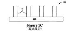
図1A,1B,1Cは、FinFETのフィン構造の従来の形成方法を概念的に示す。これらの図は、フィン構造を形成するために使用される材料層の断面図100を示している。図1Aに示す実施形態では、誘電層110(二酸化シリコンなど)の上に、半導体材料の層105(単結晶シリコン、シリコンゲルマニウムまたはゲルマニウムなど)が形成される。次に、半導体材料の層105の上に酸化物層115が形成される。酸化物層115は、後から他の構造を形成および/またはエッチングするための、層105の保護層として機能しうる。また、酸化物層115は、後から堆積する層(例えば窒化物層)のための応力低減層としても機能しうる。一部の実施形態では、別の窒化物層120が堆積される。次に、窒化物層の上にフォトレジスト層が形成され(この層は、例えばマスクを使用してパターニングされ)、パターンを窒化物層に転写するために使用されうる。パターニングされた窒化物層120は、図1Bに示すフィン構造125を形成するために、酸化物層115と層105をエッチングするためのマスクとして使用される。一実施形態では、パターニングされた窒化物層120と酸化物層115が除去され、図1Cに示すフィン構造125が残されうる。 1A, 1B, and 1C conceptually show a conventional method of forming a FinFET fin structure. These figures show a
図2は、FinFET技術を使用して形成された従来のトランジスタ200の上面図を概念的に示す。トランジスタ200は、ソース210とドレイン215の間にゲート電極205を有する。図1A〜Cに示す薄型構造125などのフィン構造220がソース210とドレイン215の間に形成され、これらの構造は、ゲート電極205の下に延びている。FinFETの例と、FinFETの形成に使用されうる技術とは、ラオおよびマシューによる米国特許第7,265,059号明細書、バーネットらによる米国特許出願公開第2007/0161171号明細書、ならびにハリスらによる"Fin-FETs: Challenges in Material and Processing for a New 3-D Device Paradigm"(新しい三次元デバイスパラダイムのための材料および処理における課題),FUTURE FAB International,23号に開示されている。 FIG. 2 conceptually illustrates a top view of a
従来のFinFETのフィン構造は、FinFETを採用しているCMOS装置に、比較的高い駆動電流を供給するように構成されうる。しかし、従来のフィン構造は、1つの配向を有し、1つの材料から形成される。したがって、従来のフィン構造は、高い駆動電流を供給するために、1種類のCMOS装置に対してしか最適化できない。すなわち、フィン構造を、高いホール移動度が求められるPMOSデバイスか、高い電子移動度が求められるNMOSデバイスの一方についてしか最適化することができない。回路設計の大部分は、PMOSデバイスとNMOSデバイスを多数備える。回路の形成に使用されるプロセスフローを、一方の種類のデバイスのみについて最適化できるが、この結果、もう一方の種類のデバイスのプロセスフローが最適化されないこととなる。 The fin structure of a conventional FinFET can be configured to supply a relatively high drive current to a CMOS device that employs a FinFET. However, conventional fin structures have one orientation and are formed from one material. Thus, the conventional fin structure can only be optimized for one type of CMOS device to supply a high drive current. That is, the fin structure can be optimized only for one of a PMOS device requiring high hole mobility or an NMOS device requiring high electron mobility. Most circuit designs comprise a large number of PMOS and NMOS devices. The process flow used to form the circuit can be optimized for only one type of device, but this results in the process flow of the other type of device not being optimized.
ここに記載の主題は、上に記載の課題の1つ以上の影響を解決することを対象とする。 The subject matter described herein is directed to solving one or more of the effects of the problems described above.
以下では、本発明の一部の態様の基本を理解できるように、ここに記載の主題の概要を説明する。当該記載内容は、ここに記載の本主題の概略を記載するが、すべてを網羅するものではない。本発明の主要または重要な要素を特定したり、本発明の範囲を詳細に記載することを意図するものでもない。その唯一の目的は、下で説明する詳細な説明に先だって、概念の一部を簡潔に示すことにある。 The following presents a summary of the subject matter described herein so that the basis of some aspects of the invention may be understood. The description provides an overview of the subject matter described herein, but is not exhaustive. It is not intended to identify key or critical elements of the invention or to delineate the scope of the invention. Its sole purpose is to present some of the concepts in a concise manner prior to the detailed description below.
一実施形態では、トランジスタの形成方法が提供される。前記方法は、絶縁層の上に第1の半導体材料の第1の層を形成するステップを有する。 In one embodiment, a method for forming a transistor is provided. The method includes forming a first layer of a first semiconductor material on an insulating layer.
前記第1の半導体材料は、第1のキャリア型に高い移動度を与えるように選択されている。また、前記方法は、前記第1の層の上に、第2の半導体材料の第2の層を形成するステップも有する。前記第2の半導体材料は、前記第1のキャリア型とは逆の第2のキャリア型に高い移動度を与えるように選択されている。前記方法は、前記第2の層に隣接して第1のマスク層を形成するステップと、前記第2の層に少なくとも1つの特徴を形成するために、前記第1のマスク層を介して前記第2の層をエッチングするステップと、を有する。前記第2の層内の各特徴は、前記第2の層の一部と共に逆T字形状を形成する。 The first semiconductor material is selected to give high mobility to the first carrier type. The method also includes forming a second layer of a second semiconductor material on the first layer. The second semiconductor material is selected to give a high mobility to a second carrier type opposite to the first carrier type. The method includes forming a first mask layer adjacent to the second layer, and through the first mask layer to form at least one feature in the second layer. Etching the second layer. Each feature in the second layer forms an inverted T shape with a portion of the second layer.
別の実施形態では、トランジスタが提供される。前記トランジスタは、埋め込み酸化物層の上に設けた、第1の半導体材料から形成された第1の層を有する。前記第1の半導体材料は、第1のキャリア型に高い移動度を与えるように選択されている。また、前記トランジスタは、前記第1の層に隣接して、第2の半導体材料から形成された第2の層も有する。前記第2の半導体材料は、前記第1のキャリア型とは逆の第2のキャリア型に高い移動度を与えるように選択されている。また、前記第2の層は、前記第2の層内の各特徴が、前記第1の層の一部と共に逆T字形状を形成するように、第1のマスク層を介して前記第2の層をエッチングすることによって前記第2の層に形成された少なくとも1つの特徴を有する。 In another embodiment, a transistor is provided. The transistor has a first layer made of a first semiconductor material provided over a buried oxide layer. The first semiconductor material is selected to give high mobility to the first carrier type. The transistor also has a second layer formed from a second semiconductor material adjacent to the first layer. The second semiconductor material is selected to give a high mobility to a second carrier type opposite to the first carrier type. In addition, the second layer has the second mask through the first mask layer so that each feature in the second layer forms an inverted T shape together with a part of the first layer. At least one feature formed in the second layer by etching the second layer.
添付の図面と併せて下記の説明を読めば、本主題が理解されるであろう。添付の図面においては、同一の参照符号は同じ要素を参照している。 The subject matter will be understood upon reading the following description in conjunction with the accompanying drawings. In the accompanying drawings, the same reference signs refer to the same elements.
本発明は、種々の変形および代替形態を取り得るが、その具体的な実施形態が、図面に例として図示され、ここに詳細に記載されているに過ぎない。しかし、この詳細な説明は、本発明を特定の実施形態に限定することを意図するものではなく、反対に、添付の特許請求の範囲によって規定される本発明の範囲に含まれるすべての変形例、均等物および代替例を含むことを理解すべきである。 While the invention is susceptible to various modifications and alternative forms, specific embodiments thereof are shown by way of example in the drawings and are herein described in detail. However, this detailed description is not intended to limit the invention to the specific embodiments, but on the contrary, all variations that fall within the scope of the invention as defined by the appended claims. It should be understood that equivalents and alternatives are included.
本主題の例示的な実施形態を下記に記載する。簡潔を期すために、実際の実装の特徴をすべて本明細書に記載することはしない。当然、実際の実施形態の開発においては、システム上の制約およびビジネス上の制約に適合させるなど、開発の具体的な目的を達成するために、実装に固有の判断が数多く必要とされ、これは実装によって変わるということが理解される。更に、この種の開発作業は複雑かつ時間がかかるものであるが、本開示の利益を受ける当業者にとって日常的な作業であるということを理解されたい。 Exemplary embodiments of the present subject matter are described below. For the sake of brevity, not all features of an actual implementation are described here. Of course, developing an actual embodiment requires a number of implementation specific decisions to achieve specific development goals, such as adapting to system and business constraints. It is understood that it varies depending on the implementation. Further, it should be understood that this type of development work is complex and time consuming, but is routine for those skilled in the art who benefit from the present disclosure.
次に、添付の図面を参照して本主題を説明する。説明のみを目的として、当業者に知られている細かい点を説明して本開示をわかりにくくすることのないように、さまざまな構造、システムおよびデバイスが、図面で模式的に示されている。しかし、ここに記載の主題の例示的な例を記載および説明するために、添付の図面を添付する。本明細書において使用される語句は、関連技術の当業者が理解している意味と同じ意味に使用されていると理解および解釈すべきである。本明細書においてある語句が矛盾なく用いられている場合、その語句が特別な定義を有する、すなわち通常かつ慣用的に用いられ、当業者が理解している意味と異なる定義を有することはない。ある語句が特別な意味を有する、すなわち当業者の理解とは異なる意味に用いられる場合は、そのような特別な定義は本明細書に明示的に記載して、その特別な定義を直接的かつ明確に示す。 The subject matter will now be described with reference to the attached figures. For purposes of explanation only, various structures, systems and devices are schematically shown in the drawings so as not to obscure the present disclosure with details that are known to those skilled in the art. However, the attached drawings are included to describe and explain illustrative examples of the subject matter described herein. The terms used herein should be understood and interpreted to have the same meaning as understood by those of ordinary skill in the relevant art. When a phrase is used consistently in this specification, the phrase has a special definition, i.e. it is used normally and routinely and does not have a definition different from the meaning understood by those skilled in the art. When a word has a special meaning, i.e. used in a meaning that is different from the understanding of those skilled in the art, such special definition is explicitly stated herein and the special definition is directly and directly Show clearly.
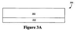
図3A,3B,3C,3D,3Eは、ヘテロ構造逆T字フィン構造の形成方法の例示的な一実施形態を概念的に示す。これらの図は、ヘテロ構造逆T字フィン構造を形成するために使用される材料層の断面図300を示す。図3Aに示す実施形態では、誘電層310に隣接して、半導体材料の第1の層305が形成される。層305の形成に使用する半導体材料は、比較的高いホールまたは電子の移動度を与えるように選択されうる。ここで使用される「隣接する」という用語は、第1の層305と誘電層310が、場合によっては接することもあるが、両者が必ずしも接していることを指すとは限らない。一部の実施形態では、隣接する第1の層305と誘電層310との間に1層以上の層が形成されてもよい。誘電層310は二酸化シリコンまたは他の絶縁材料から形成される埋め込み酸化物層であってもよく、第1の層305はシリコン層であってもよい。別の実施形態では、層305は、歪みシリコンオンインシュレータ層305であってもよい。シリコン、シリコンオンインシュレータおよび/または歪みシリコンオンインシュレータ層305を形成するための技術は、当業者に知られており、簡潔を期するためにのみ、本発明に関連するこのような層305を形成する態様を以下に説明する。 3A, 3B, 3C, 3D, 3E conceptually illustrate one exemplary embodiment of a method for forming a heterostructure inverted T-fin structure. These figures show a
引張歪みまたは圧縮歪みを有するシリコンオンインシュレータ層305を使用することより、ヘテロ構造逆T字フィン構造における、電子および/またはホールの移動度の制御、変更および/または向上が可能となる。例えば、シリコンオンインシュレータ層305を歪ませることにより、歪みシリコンオンインシュレータ層305の伝導性および/または価電子帯構造を変化させて、電子および/またはホールの移動度を上げることができる。更に、歪みシリコンオンインシュレータ層305のシリコン格子を歪ませることによって、格子不整合欠陥の発生を低減させることにより、高品質のエピタキシャル層(例えば、後述するゲルマニウム層)の成長を促進することができる。移動度の制御および/または格子不整合欠陥の低減や、その他の目的のために、シリコンオンインシュレータ層305を歪ませるための技術は、従来技術において公知であり、簡潔を期するために、ここに更に記載することはしない。 By using the silicon-on-
次に、図3Bに示すように、第1の層305の上に、異なる種類の半導体材料の第2の層315が、第1の層305と第2の層315とが隣接するように形成される。第1の層305に使用する材料が、比較的高い電子の移動度を与えるように選択される場合には、第2の層315の形成に使用する半導体材料は、比較的高いホールの移動度を与えるように選択されうる。例えば、第1の層305がシリコンオンインシュレータから形成される場合、第2の層315はゲルマニウムから形成されうる。一実施形態では、ゲルマニウム層315は、形成時にドープされても(intrinsically doped)も、堆積後に、例えばイオン注入法を使用してドープされてもよい。ゲルマニウム層315を形成するための技術は、当業者に知られており、簡潔を期するためにのみ、本発明に関連するこのような層315を形成する態様を以下に説明する。あるいは、第1の層305に使用する材料が、比較的高いホールの移動度を与えるように選択される場合には、第2の層315の形成に使用する半導体材料は、比較的高い電子の移動度を与えるように選択されうる。 Next, as illustrated in FIG. 3B, a
図に示した実施形態では、第1の層305と第2の層315を形成するためにシリコンとゲルマニウムが使用されるが、本開示の利益を享受する当業者は、本発明が、これらの材料から第1の層305と第2の層315を形成することに限定されないことを理解するであろう。別の実施形態では、層305,315の一方で電子の移動度が比較的高くなり、層305,315のもう一方で比較的高いホールの移動度を与えるように、半導体材料のほかの組み合せが選択されてもよい。第1の層305と第2の層315の形成に使用することができる材料の組み合せの例としては、第1の層305にゲルマニウムを、第2の層315にシリコンを使用する例、第1の層305にGaAsを、第2の層315にゲルマニウムを使用する例、第1の層305にシリコンを、第2の層315にGaAsを使用する例などが挙げられる。 In the illustrated embodiment, silicon and germanium are used to form the
次に、図3Cに示すように、第2の層315の上に絶縁体層320(酸化物など)が形成される。例えば、絶縁体層320は、第2の層315の上に酸化物(二酸化シリコンなど)を堆積させることによって形成されうる。別の実施形態では、第2の層315の上部分を酸化させることによって、絶縁体層320が形成されてもよい。一実施形態では、絶縁体層320は、後から他の構造を形成および/またはエッチングする際の保護層として機能しうる。次に、絶縁体層320の上に別の層325が形成され、層325がフォトレジストを使用してパターニングされうる。パターニングされたマスク層325は、各種の材料(例えば窒化物層など)から形成することができる。マスク層325に設けたパターンは、第2の層315のエッチングによって形成しようとしている構造のパターンに対応している。例えば、このパターンは、第1の層305と第2の層315の間の界面によって規定される平面で、この構造の寸法(幅と長さなど)を規定しうる。また、第2の層315の膜厚によって、当該構造の第3の寸法(高さなど)が規定されうる。 Next, as illustrated in FIG. 3C, an insulator layer 320 (oxide or the like) is formed over the
次に、図3Dに示すように、パターニングされたマスク層325をマスクとして使用して、絶縁体層320と第2の層315とがエッチングされうる。第2の層315のエッチングは、エッチストップ技術(例えば、発光分光分析など)を使用するか、あるいは、エッチングプロセスの時間を測ることによって停止されうる。エッチングは、好ましくは、エッチングプロセスにより第1の層305の一部がエッチングされる前に停止される。しかし、本開示の利益を享受する当業者は、第1の層305が一切エッチングされないように正確にエッチングを制御することが困難となりうることを理解するであろう。このため、エッチングプロセスの現実的な実装では、第2の層315のマスクされていない部分が(一定の許容誤差内で)実質的にすべてエッチングされ、第1の層305が(一定の許容誤差内で)実質的にエッチングされないタイミングで、エッチングプロセスを停止させようとする。エッチングプロセスにより、絶縁体層320と第2の層315のエッチングされていない部分を含むフィン状構造330が形成される。一実施形態では、フィン状構造330の幅(すなわち、図の紙面における寸法)は、フィン状構造330の深さ(すなわち、図の紙面に直交する寸法)よりも短い。一実施形態では、フィン状構造330の厚みは、絶縁体層320と第2の層315の膜厚にほぼ等しい。 Next, as shown in FIG. 3D, the
処理のこの時点で、フィン状構造330と第1の層305とは、連続する超薄体(UTB)デバイスなどの、連続するデバイスに使用されうるヘテロ構造逆T字フィン構造を形成している。例えば、フィン状構造330の高さは、実質的に15〜90nmの範囲であり、第1の層305の膜厚は、実質的に1〜60nmの範囲である。半導体材料の配向は、関連するキャリア(例えばホールまたは電子)の最も高い移動度を与えるように選択されうる。一実施形態では、第1の層305の伝導面332が、平坦な(100)形状を有し、フィン状構造330の第2の層の側面334の伝導面が、平坦な(110)形状を有するように、第1の半導体材料は、配向(100)を有するように選択されうる。別の実施形態では、高いホール移動度などの高いキャリア移動度が確実に得られるように、第1の半導体材料に、(110)配向などの異なる配向が選択されてもよい。この場合、第2の半導体材料は、(100)配向などの別の配向で形成される。 At this point in processing, the fin-
別の一実施形態では、第1の層305をパターニングすることによって、複数ゲートUTBデバイスが形成されうる。図3Eに示す実施形態では、第1の層305の一部がエッチングされて、ベース構造335が残される。第1の層305の一部をマスクおよび/またはエッチングするための技術は、従来技術において公知であり、簡潔を期するために、ここに更に記載することはない。ベース構造335は、フィン状構造330と実質的に対称に形成される。ベース構造335の幅は、フィン状構造330の幅よりも広い。例えば、ベース構造335の幅は、約60〜200nmの範囲であり、フィン状構造330の幅は、約1〜60nmの範囲である。一部の実施形態では、ベース構造335の厚みは、フィン状構造330の厚みとほぼ同じであってもよい。例えば、フィン状構造330の厚みとベース構造335の厚みはいずれも約20nmであってもよい。しかし、これは単に例示に過ぎず、全ての場合に適用されるというわけではない。この結果、ベース構造335とフィン状構造330とは、(図の紙面に)延在する逆T字構造を形成することになる。ここに図示する実施形態の例では、ベース構造335の厚みは、第1の層305の膜厚に実質的に等しい。 In another embodiment, a multi-gate UTB device can be formed by patterning the
図4は、ヘテロ構造逆T字フィン構造405を有するトランジスタ400の上面図を概念的に示す。図4の破線楕円によって、フィン構造405の2つがほぼ示されている。図に示した実施形態では、フィン構造405が、トランジスタ400のチャネル領域として動作するように、ゲート410、ソース領域415およびドレイン領域420が形成されている。ゲート410、ソース領域415およびドレイン領域420のほか、ゲート誘電体や、ゲート410、ソース415および/またはドレイン420へのコンタクトなど、トランジスタ400の他の構成要素を形成するための技術や他の後処理プロセスは、従来技術において公知である。簡潔を期するために、本発明に関連する、トランジスタ400の構成要素を形成する態様のみを以下に説明する。 FIG. 4 conceptually illustrates a top view of a
図の実施形態に示すフィン構造405は、シリコンから形成されるベース425と、ゲルマニウムから形成されるフィン430とを有する。一実施形態では、フィン構造405は、図3A〜3Eに示したプロセスに従って形成されうる。フィン状構造405は、ゲート410によって複数の方向から制御される。この結果、トランジスタ400は、従来の平面型トランジスタを使用するトランジスタよりも、短チャネル効果に対して耐性を備えることができる。トランジスタ400のデバイス形状は、材料および/または配向によるホールおよび/または電子の移動度依存性を最適化して、図1Cに示すような、従来のI字状(またはバー形状)のフィンを使用するトランジスタよりも高い駆動電流を供給するように選択されうる。例えば、トランジスタ400がPMOSデバイスとして実装される場合、フィン430のゲルマニウムの一部(例えば部分315など)では、ホールの移動度が比較的高くなっている。更に、フィン430の側壁(図示せず)の(110)形状は、平面形状の(100)伝導面よりもホール移動度が高い。同じトランジスタ400がNMOSデバイスとして実装される場合、水平のシリコンのベース425の(100)伝導面は、電子の移動度が高い。シリコンのベース425の電子移動度とゲルマニウムのフィン430のホール移動度とが対称であることにより、チップ面積の最適化が可能となる一方で、トランジスタ400のオン電流を対称に保持できる。 The
また、トランジスタ400が他の方法で変更されてもよい。例えば、ベース425とフィン430によって形成されるチャンネル領域は、形成時にドープされても(intrinsically doped)も、例えば、イオン注入技術とアニール技術を使用してドープされてもよい。別の例では、拡張注入を使用して、あるいは、ソース領域410および/またはドレイン領域415からのドーパントのアンダーラップを使用して拡張部が形成されてもよい。更に別の例では、トランジスタ400に形成されるスペーサの領域の外で、ゲルマニウムおよび/またはシリコンを選択的にエピタキシャル成長させ、寄生抵抗を低減させてもよい。 The
図5Aは、連続する超薄体(UTB)デバイス500の斜視図を概念的に示す。図に示した実施形態では、UTBデバイス500は、基板505上に形成され、ヘテロ構造逆T字フィン構造を形成するフィン状構造510および第1の層515を備える。フィン状構造510は、第1のキャリア型(ホールなど)の移動度を比較的高くするように選択された第1の材料から形成され、第1の層515は、第2のキャリア型(電子など)の移動度を比較的高くするように選択された第2の材料から形成される。続いて、ヘテロ構造逆T字フィン構造の上に、層520が形成される。層520は、ゲート、ソースおよび/またはドレイン構造を形成するために使用されうる。 FIG. 5A conceptually illustrates a perspective view of a continuous ultrathin body (UTB)
図5Bは、複数ゲート超薄体(UTB)デバイス525の斜視図を概念的に示す。図に示した実施形態では、UTBデバイス525は、基板530上に形成され、ヘテロ構造逆T字フィン構造を形成するフィン状構造535およびベース構造540とを備える。フィン状構造535は、第1のキャリア型(ホールなど)の移動度を比較的高くするように選択された第1の材料から形成され、ベース構造540は、第2のキャリア型(電子など)の移動度を比較的高くするように選択された第2の材料から形成される。続いて、ヘテロ構造逆T字フィン構造の上に、層545が形成される。層545は、ゲート、ソースおよび/またはドレイン構造を形成するために使用されうる。 FIG. 5B conceptually illustrates a perspective view of a multi-gate ultrathin body (UTB)
上記に記載した特定の実施形態は例に過ぎず、本発明は、本開示の教示の利益を得る当業者にとって自明の、異なるが均等の別法によって変更および実施されてもよい。更に、ここに記載した構成または設計の詳細が、添付の特許請求の範囲以外によって限定されることない。このため、上記に記載した特定の実施形態を変形または変更することが可能であり、このような変形例はすべて本発明の範囲に含まれることが意図されることが明らかである。したがって、ここに保護を請求する対象は、添付の特許請求の範囲に記載したとおりである。 The specific embodiments described above are merely examples, and the invention may be modified and implemented by different but equivalent alternatives, which will be apparent to those skilled in the art having the benefit of the teachings of the disclosure. Further, the details of construction or design described herein are not limited except as by the appended claims. For this reason, it is obvious that the specific embodiments described above can be modified or changed, and all such modifications are intended to be included within the scope of the present invention. Accordingly, the subject matter claimed for protection herein is as set forth in the appended claims.
Claims (10)
Translated fromJapanese前記第1の層の上に、前記第1のキャリア型とは逆の第2のキャリア型に高い移動度を与えるように選択された第2の半導体材料の第2の層を形成するステップと、
前記第1の層内の各特徴が、前記第2の層の一部と共に逆T字形状構造のベースを形成するように、前記第2の層に少なくとも1つの特徴を形成するために、前記第2の層をエッチングするステップと、を含む、トランジスタの形成方法。Forming a first layer of a first semiconductor material on the insulating layer selected to provide high mobility for the first carrier type;
Forming on the first layer a second layer of a second semiconductor material selected to provide high mobility to a second carrier type opposite to the first carrier type; ,
To form at least one feature in the second layer such that each feature in the first layer forms a base of an inverted T-shaped structure with a portion of the second layer. Etching the second layer. A method of forming a transistor.
前記第1の層に隣接して、前記第1のキャリア型とは逆の第2のキャリア型に高い移動度を与えるように選択された第2の半導体材料から形成された第2の層とを備え、前記第2の層は、前記第2の層内の各特徴が、前記第1の層の一部と共に逆T字形状構造のベースを形成するように、前記第2の層をエッチングすることによって前記第2の層に形成された少なくとも1つの特徴を有する、トランジスタ。A first layer formed on the buried oxide layer and formed from a first semiconductor material selected to provide high mobility to the first carrier type;
A second layer formed of a second semiconductor material adjacent to the first layer and selected to provide high mobility to a second carrier type opposite to the first carrier type; And etching the second layer such that each feature in the second layer forms a base of an inverted T-shaped structure with a portion of the first layer. A transistor having at least one feature formed in the second layer.
Applications Claiming Priority (3)
| Application Number | Priority Date | Filing Date | Title |
|---|---|---|---|
| US11/948,235 | 2007-11-30 | ||
| US11/948,235US8288756B2 (en) | 2007-11-30 | 2007-11-30 | Hetero-structured, inverted-T field effect transistor |
| PCT/US2008/013041WO2009070252A1 (en) | 2007-11-30 | 2008-11-21 | A hetero-structured, inverted-t field effect transistor |
Publications (3)
| Publication Number | Publication Date |
|---|---|
| JP2011505697Atrue JP2011505697A (en) | 2011-02-24 |
| JP2011505697A5 JP2011505697A5 (en) | 2011-06-23 |
| JP5498394B2 JP5498394B2 (en) | 2014-05-21 |
Family
ID=40260725
Family Applications (1)
| Application Number | Title | Priority Date | Filing Date |
|---|---|---|---|
| JP2010535978AActiveJP5498394B2 (en) | 2007-11-30 | 2008-11-21 | Transistor and method for forming the same |
Country Status (7)
| Country | Link |
|---|---|
| US (2) | US8288756B2 (en) |
| EP (1) | EP2220686A1 (en) |
| JP (1) | JP5498394B2 (en) |
| KR (1) | KR101392436B1 (en) |
| CN (1) | CN101884107B (en) |
| TW (1) | TWI450339B (en) |
| WO (1) | WO2009070252A1 (en) |
Families Citing this family (12)
| Publication number | Priority date | Publication date | Assignee | Title |
|---|---|---|---|---|
| JP5285947B2 (en)* | 2008-04-11 | 2013-09-11 | 株式会社東芝 | Semiconductor device and manufacturing method thereof |
| US8101486B2 (en)* | 2009-10-07 | 2012-01-24 | Globalfoundries Inc. | Methods for forming isolated fin structures on bulk semiconductor material |
| US8815677B2 (en)* | 2011-06-14 | 2014-08-26 | Intermolecular, Inc. | Method of processing MIM capacitors to reduce leakage current |
| CN102956686A (en)* | 2011-08-18 | 2013-03-06 | 中国科学院微电子研究所 | Silicon-based germanium nano-structure substrate and preparation method thereof |
| FR2982421A1 (en)* | 2011-11-09 | 2013-05-10 | Soitec Silicon On Insulator | Semiconductor device for use on semiconductor on insulator substrate, has grid whose back area is formed in massive substrate under insulating layer, where insulating layer electrically isolates back area of grid from semiconductor body |
| US9583398B2 (en)* | 2012-06-29 | 2017-02-28 | Taiwan Semiconductor Manufacturing Company, Ltd. | Integrated circuit having FinFETS with different fin profiles |
| US9142400B1 (en) | 2012-07-17 | 2015-09-22 | Stc.Unm | Method of making a heteroepitaxial layer on a seed area |
| CN103871885B (en)* | 2012-12-18 | 2016-08-10 | 中芯国际集成电路制造(上海)有限公司 | Fin field effect transistor manufacturing method |
| CN104103506B (en)* | 2013-04-11 | 2018-02-13 | 中国科学院微电子研究所 | Semiconductor device manufacturing method |
| US20170309623A1 (en)* | 2016-04-21 | 2017-10-26 | Globalfoundries Inc. | Method, apparatus, and system for increasing drive current of finfet device |
| CN111383917B (en)* | 2018-12-29 | 2023-02-21 | 中芯国际集成电路制造(上海)有限公司 | Semiconductor structure and forming method thereof |
| CN118213404B (en)* | 2024-03-06 | 2025-10-03 | 西安电子科技大学广州研究院 | Enhanced-mode p-channel gallium nitride field-effect transistor and preparation method thereof |
Citations (10)
| Publication number | Priority date | Publication date | Assignee | Title |
|---|---|---|---|---|
| US6475890B1 (en)* | 2001-02-12 | 2002-11-05 | Advanced Micro Devices, Inc. | Fabrication of a field effect transistor with an upside down T-shaped semiconductor pillar in SOI technology |
| JP2005045263A (en)* | 2003-07-23 | 2005-02-17 | Samsung Electronics Co Ltd | Pin field effect transistor and method of forming the same |
| JP2005051241A (en)* | 2003-07-25 | 2005-02-24 | Interuniv Micro Electronica Centrum Vzw | Multilayer gate semiconductor device and manufacturing method thereof |
| JP2006501672A (en)* | 2002-09-30 | 2006-01-12 | アドバンスト・マイクロ・ディバイシズ・インコーポレイテッド | FinFET with improved carrier mobility and method of forming the same |
| JP2006093717A (en)* | 2004-09-25 | 2006-04-06 | Samsung Electronics Co Ltd | Field effect transistor having a deformed channel layer and method for manufacturing the same |
| WO2006125040A2 (en)* | 2005-05-17 | 2006-11-23 | Amberwave Systems Corporation | Lattice-mismatched semiconductor structures with reduced dislocation defect densities related methods for device fabrication |
| JP2007509496A (en)* | 2003-10-22 | 2007-04-12 | コミツサリア タ レネルジー アトミーク | Field effect microelectronic device capable of forming one or more transistor channels |
| US20070148837A1 (en)* | 2005-12-27 | 2007-06-28 | Uday Shah | Method of fabricating a multi-cornered film |
| JP2007258485A (en)* | 2006-03-23 | 2007-10-04 | Toshiba Corp | Semiconductor device and manufacturing method thereof |
| US20070235763A1 (en)* | 2006-03-29 | 2007-10-11 | Doyle Brian S | Substrate band gap engineered multi-gate pMOS devices |
Family Cites Families (28)
| Publication number | Priority date | Publication date | Assignee | Title |
|---|---|---|---|---|
| JPS60210831A (en)* | 1984-04-04 | 1985-10-23 | Agency Of Ind Science & Technol | Manufacture of compound semiconductor crystal substrate |
| JPH073814B2 (en)* | 1984-10-16 | 1995-01-18 | 松下電器産業株式会社 | Method for manufacturing semiconductor substrate |
| EP0323896B1 (en)* | 1988-01-07 | 1996-04-17 | Fujitsu Limited | Complementary semiconductor device |
| US5466949A (en)* | 1994-08-04 | 1995-11-14 | Texas Instruments Incorporated | Silicon oxide germanium resonant tunneling |
| US6362071B1 (en)* | 2000-04-05 | 2002-03-26 | Motorola, Inc. | Method for forming a semiconductor device with an opening in a dielectric layer |
| US6600170B1 (en)* | 2001-12-17 | 2003-07-29 | Advanced Micro Devices, Inc. | CMOS with strained silicon channel NMOS and silicon germanium channel PMOS |
| US6605514B1 (en)* | 2002-07-31 | 2003-08-12 | Advanced Micro Devices, Inc. | Planar finFET patterning using amorphous carbon |
| US6872647B1 (en)* | 2003-05-06 | 2005-03-29 | Advanced Micro Devices, Inc. | Method for forming multiple fins in a semiconductor device |
| CN1799146A (en)* | 2003-05-30 | 2006-07-05 | 松下电器产业株式会社 | Semiconductor device and method for manufacturing same |
| US7045401B2 (en)* | 2003-06-23 | 2006-05-16 | Sharp Laboratories Of America, Inc. | Strained silicon finFET device |
| EP1519420A2 (en) | 2003-09-25 | 2005-03-30 | Interuniversitaire Microelectronica Centrum vzw ( IMEC) | Multiple gate semiconductor device and method for forming same |
| US6855583B1 (en)* | 2003-08-05 | 2005-02-15 | Advanced Micro Devices, Inc. | Method for forming tri-gate FinFET with mesa isolation |
| US20050116290A1 (en)* | 2003-12-02 | 2005-06-02 | De Souza Joel P. | Planar substrate with selected semiconductor crystal orientations formed by localized amorphization and recrystallization of stacked template layers |
| US7041576B2 (en)* | 2004-05-28 | 2006-05-09 | Freescale Semiconductor, Inc. | Separately strained N-channel and P-channel transistors |
| KR100674914B1 (en) | 2004-09-25 | 2007-01-26 | 삼성전자주식회사 | Morse transistor having a modified channel layer and method of manufacturing same |
| US7393733B2 (en)* | 2004-12-01 | 2008-07-01 | Amberwave Systems Corporation | Methods of forming hybrid fin field-effect transistor structures |
| JP2008529295A (en)* | 2005-01-28 | 2008-07-31 | エヌエックスピー ビー ヴィ | Method for manufacturing a dual gate FET |
| US7470951B2 (en)* | 2005-01-31 | 2008-12-30 | Freescale Semiconductor, Inc. | Hybrid-FET and its application as SRAM |
| US20060214233A1 (en)* | 2005-03-22 | 2006-09-28 | Ananthanarayanan Hari P | FinFET semiconductor device |
| US7344962B2 (en)* | 2005-06-21 | 2008-03-18 | International Business Machines Corporation | Method of manufacturing dual orientation wafers |
| US7323389B2 (en)* | 2005-07-27 | 2008-01-29 | Freescale Semiconductor, Inc. | Method of forming a FINFET structure |
| US7265059B2 (en)* | 2005-09-30 | 2007-09-04 | Freescale Semiconductor, Inc. | Multiple fin formation |
| US7709303B2 (en)* | 2006-01-10 | 2010-05-04 | Freescale Semiconductor, Inc. | Process for forming an electronic device including a fin-type structure |
| FR2896620B1 (en)* | 2006-01-23 | 2008-05-30 | Commissariat Energie Atomique | THREE-DIMENSIONAL INTEGRATED CIRCUIT OF C-MOS TYPE AND METHOD OF MANUFACTURE |
| US7544980B2 (en)* | 2006-01-27 | 2009-06-09 | Freescale Semiconductor, Inc. | Split gate memory cell in a FinFET |
| US7803670B2 (en)* | 2006-07-20 | 2010-09-28 | Freescale Semiconductor, Inc. | Twisted dual-substrate orientation (DSO) substrates |
| WO2008039495A1 (en)* | 2006-09-27 | 2008-04-03 | Amberwave Systems Corporation | Tri-gate field-effect transistors formed by aspect ratio trapping |
| US7692254B2 (en)* | 2007-07-16 | 2010-04-06 | International Business Machines Corporation | Fin-type field effect transistor structure with merged source/drain silicide and method of forming the structure |
- 2007
- 2007-11-30USUS11/948,235patent/US8288756B2/enactiveActive
- 2008
- 2008-11-21CNCN2008801156452Apatent/CN101884107B/enactiveActive
- 2008-11-21EPEP08853153Apatent/EP2220686A1/ennot_activeCeased
- 2008-11-21KRKR1020107011883Apatent/KR101392436B1/enactiveActive
- 2008-11-21JPJP2010535978Apatent/JP5498394B2/enactiveActive
- 2008-11-21WOPCT/US2008/013041patent/WO2009070252A1/enactiveApplication Filing
- 2008-11-28TWTW097146123Apatent/TWI450339B/enactive
- 2012
- 2012-08-13USUS13/584,673patent/US8815658B2/enactiveActive
Patent Citations (10)
| Publication number | Priority date | Publication date | Assignee | Title |
|---|---|---|---|---|
| US6475890B1 (en)* | 2001-02-12 | 2002-11-05 | Advanced Micro Devices, Inc. | Fabrication of a field effect transistor with an upside down T-shaped semiconductor pillar in SOI technology |
| JP2006501672A (en)* | 2002-09-30 | 2006-01-12 | アドバンスト・マイクロ・ディバイシズ・インコーポレイテッド | FinFET with improved carrier mobility and method of forming the same |
| JP2005045263A (en)* | 2003-07-23 | 2005-02-17 | Samsung Electronics Co Ltd | Pin field effect transistor and method of forming the same |
| JP2005051241A (en)* | 2003-07-25 | 2005-02-24 | Interuniv Micro Electronica Centrum Vzw | Multilayer gate semiconductor device and manufacturing method thereof |
| JP2007509496A (en)* | 2003-10-22 | 2007-04-12 | コミツサリア タ レネルジー アトミーク | Field effect microelectronic device capable of forming one or more transistor channels |
| JP2006093717A (en)* | 2004-09-25 | 2006-04-06 | Samsung Electronics Co Ltd | Field effect transistor having a deformed channel layer and method for manufacturing the same |
| WO2006125040A2 (en)* | 2005-05-17 | 2006-11-23 | Amberwave Systems Corporation | Lattice-mismatched semiconductor structures with reduced dislocation defect densities related methods for device fabrication |
| US20070148837A1 (en)* | 2005-12-27 | 2007-06-28 | Uday Shah | Method of fabricating a multi-cornered film |
| JP2007258485A (en)* | 2006-03-23 | 2007-10-04 | Toshiba Corp | Semiconductor device and manufacturing method thereof |
| US20070235763A1 (en)* | 2006-03-29 | 2007-10-11 | Doyle Brian S | Substrate band gap engineered multi-gate pMOS devices |
Also Published As
| Publication number | Publication date |
|---|---|
| KR101392436B1 (en) | 2014-05-07 |
| KR20100098516A (en) | 2010-09-07 |
| TW200937535A (en) | 2009-09-01 |
| US8815658B2 (en) | 2014-08-26 |
| JP5498394B2 (en) | 2014-05-21 |
| US20090140294A1 (en) | 2009-06-04 |
| EP2220686A1 (en) | 2010-08-25 |
| US8288756B2 (en) | 2012-10-16 |
| WO2009070252A1 (en) | 2009-06-04 |
| TWI450339B (en) | 2014-08-21 |
| US20120309141A1 (en) | 2012-12-06 |
| CN101884107A (en) | 2010-11-10 |
| CN101884107B (en) | 2013-02-13 |
Similar Documents
| Publication | Publication Date | Title |
|---|---|---|
| JP5498394B2 (en) | Transistor and method for forming the same | |
| US6709982B1 (en) | Double spacer FinFET formation | |
| US8786057B2 (en) | Integrated circuit on corrugated substrate | |
| US7265008B2 (en) | Method of IC production using corrugated substrate | |
| US9490340B2 (en) | Methods of forming nanowire devices with doped extension regions and the resulting devices | |
| US7247887B2 (en) | Segmented channel MOS transistor | |
| US9431512B2 (en) | Methods of forming nanowire devices with spacers and the resulting devices | |
| KR102609555B1 (en) | Field effect transistor, cmos system on chip, and method of manufacturing the same | |
| US20090001470A1 (en) | Method for forming acute-angle spacer for non-orthogonal finfet and the resulting structure | |
| US20160293761A1 (en) | Finfets having strained channels, and methods of fabricating finfets having strained channels | |
| US20090289304A1 (en) | Co-integration of multi-gate fet with other fet devices in cmos technology | |
| JP2006522488A (en) | Method for forming a structure in a FINFET device | |
| TW201403825A (en) | Integrated circuit device and method of manufacturing same | |
| CN105336772B (en) | Fin type TFET (thin film transistor) and manufacturing method thereof | |
| KR101026479B1 (en) | Semiconductor element and manufacturing method thereof | |
| CN103022039A (en) | Sram unit and manufacturing method thereof | |
| US9634123B2 (en) | FinFET device including a dielectrically isolated silicon alloy fin | |
| KR102133208B1 (en) | Field-effect transistor without punch-through stopper and fabrication method thereof | |
| CN104347508B (en) | Semiconductor structure and formation method thereof | |
| CN104952730A (en) | Semiconductor structure and formation method thereof | |
| CN114446786A (en) | Method of forming a semiconductor structure | |
| JP2017517895A (en) | Method for manufacturing high performance low power field effect transistor devices with minimal or no surface roughness scattering |
Legal Events
| Date | Code | Title | Description |
|---|---|---|---|
| A521 | Request for written amendment filed | Free format text:JAPANESE INTERMEDIATE CODE: A523 Effective date:20110427 | |
| A621 | Written request for application examination | Free format text:JAPANESE INTERMEDIATE CODE: A621 Effective date:20110427 | |
| A131 | Notification of reasons for refusal | Free format text:JAPANESE INTERMEDIATE CODE: A131 Effective date:20130313 | |
| A977 | Report on retrieval | Free format text:JAPANESE INTERMEDIATE CODE: A971007 Effective date:20130314 | |
| A601 | Written request for extension of time | Free format text:JAPANESE INTERMEDIATE CODE: A601 Effective date:20130607 | |
| A602 | Written permission of extension of time | Free format text:JAPANESE INTERMEDIATE CODE: A602 Effective date:20130614 | |
| A521 | Request for written amendment filed | Free format text:JAPANESE INTERMEDIATE CODE: A523 Effective date:20130716 | |
| TRDD | Decision of grant or rejection written | ||
| A01 | Written decision to grant a patent or to grant a registration (utility model) | Free format text:JAPANESE INTERMEDIATE CODE: A01 Effective date:20140219 | |
| A61 | First payment of annual fees (during grant procedure) | Free format text:JAPANESE INTERMEDIATE CODE: A61 Effective date:20140307 | |
| R150 | Certificate of patent or registration of utility model | Ref document number:5498394 Country of ref document:JP Free format text:JAPANESE INTERMEDIATE CODE: R150 | |
| R250 | Receipt of annual fees | Free format text:JAPANESE INTERMEDIATE CODE: R250 | |
| R250 | Receipt of annual fees | Free format text:JAPANESE INTERMEDIATE CODE: R250 | |
| R250 | Receipt of annual fees | Free format text:JAPANESE INTERMEDIATE CODE: R250 | |
| R250 | Receipt of annual fees | Free format text:JAPANESE INTERMEDIATE CODE: R250 | |
| R250 | Receipt of annual fees | Free format text:JAPANESE INTERMEDIATE CODE: R250 | |
| R250 | Receipt of annual fees | Free format text:JAPANESE INTERMEDIATE CODE: R250 | |
| R250 | Receipt of annual fees | Free format text:JAPANESE INTERMEDIATE CODE: R250 | |
| R250 | Receipt of annual fees | Free format text:JAPANESE INTERMEDIATE CODE: R250 | |
| R250 | Receipt of annual fees | Free format text:JAPANESE INTERMEDIATE CODE: R250 |