JP2011259293A - Digital filter - Google Patents
Digital filterDownload PDFInfo
- Publication number
- JP2011259293A JP2011259293AJP2010133039AJP2010133039AJP2011259293AJP 2011259293 AJP2011259293 AJP 2011259293AJP 2010133039 AJP2010133039 AJP 2010133039AJP 2010133039 AJP2010133039 AJP 2010133039AJP 2011259293 AJP2011259293 AJP 2011259293A
- Authority
- JP
- Japan
- Prior art keywords
- filter
- digital filter
- analog
- impulse response
- output
- Prior art date
- Legal status (The legal status is an assumption and is not a legal conclusion. Google has not performed a legal analysis and makes no representation as to the accuracy of the status listed.)
- Withdrawn
Links
- 230000001360synchronised effectEffects0.000claimsabstractdescription3
- 230000004044responseEffects0.000claimsdescription31
- 230000010354integrationEffects0.000claimsdescription10
- 238000005070samplingMethods0.000claimsdescription8
- 238000001514detection methodMethods0.000description23
- 239000003990capacitorSubstances0.000description12
- 238000010586diagramMethods0.000description11
- 230000008859changeEffects0.000description5
- 238000000034methodMethods0.000description2
- 230000008569processEffects0.000description2
- 230000002238attenuated effectEffects0.000description1
- 230000015556catabolic processEffects0.000description1
- 230000000052comparative effectEffects0.000description1
- 238000006731degradation reactionMethods0.000description1
- 230000001934delayEffects0.000description1
- 230000003111delayed effectEffects0.000description1
- 238000001914filtrationMethods0.000description1
- 230000007246mechanismEffects0.000description1
Images


Classifications
- H—ELECTRICITY
- H03—ELECTRONIC CIRCUITRY
- H03H—IMPEDANCE NETWORKS, e.g. RESONANT CIRCUITS; RESONATORS
- H03H17/00—Networks using digital techniques
- H03H17/02—Frequency selective networks
- H03H17/0283—Filters characterised by the filter structure
- H03H17/0286—Combinations of filter structures
- H—ELECTRICITY
- H03—ELECTRONIC CIRCUITRY
- H03H—IMPEDANCE NETWORKS, e.g. RESONANT CIRCUITS; RESONATORS
- H03H17/00—Networks using digital techniques
- H03H17/02—Frequency selective networks
- H03H17/0248—Filters characterised by a particular frequency response or filtering method
- H03H17/026—Averaging filters
- H—ELECTRICITY
- H03—ELECTRONIC CIRCUITRY
- H03H—IMPEDANCE NETWORKS, e.g. RESONANT CIRCUITS; RESONATORS
- H03H17/00—Networks using digital techniques
- H03H17/02—Frequency selective networks
- H03H17/0248—Filters characterised by a particular frequency response or filtering method
- H03H17/0282—Sinc or gaussian filters
- H—ELECTRICITY
- H03—ELECTRONIC CIRCUITRY
- H03H—IMPEDANCE NETWORKS, e.g. RESONANT CIRCUITS; RESONATORS
- H03H17/00—Networks using digital techniques
- H03H17/02—Frequency selective networks
- H03H17/06—Non-recursive filters
- H03H17/0621—Non-recursive filters with input-sampling frequency and output-delivery frequency which differ, e.g. extrapolation; Anti-aliasing
- H03H17/0635—Non-recursive filters with input-sampling frequency and output-delivery frequency which differ, e.g. extrapolation; Anti-aliasing characterized by the ratio between the input-sampling and output-delivery frequencies
- H03H17/0671—Cascaded integrator-comb [CIC] filters
- H—ELECTRICITY
- H03—ELECTRONIC CIRCUITRY
- H03K—PULSE TECHNIQUE
- H03K17/00—Electronic switching or gating, i.e. not by contact-making and –breaking
- H03K17/94—Electronic switching or gating, i.e. not by contact-making and –breaking characterised by the way in which the control signals are generated
- H03K17/945—Proximity switches
- H03K17/955—Proximity switches using a capacitive detector
- H—ELECTRICITY
- H03—ELECTRONIC CIRCUITRY
- H03H—IMPEDANCE NETWORKS, e.g. RESONANT CIRCUITS; RESONATORS
- H03H2218/00—Indexing scheme relating to details of digital filters
- H03H2218/10—Multiplier and or accumulator units
- H—ELECTRICITY
- H03—ELECTRONIC CIRCUITRY
- H03K—PULSE TECHNIQUE
- H03K2217/00—Indexing scheme related to electronic switching or gating, i.e. not by contact-making or -breaking covered by H03K17/00
- H03K2217/94—Indexing scheme related to electronic switching or gating, i.e. not by contact-making or -breaking covered by H03K17/00 characterised by the way in which the control signal is generated
- H03K2217/96—Touch switches
- H03K2217/9607—Capacitive touch switches
- H03K2217/960735—Capacitive touch switches characterised by circuit details
- H03K2217/960745—Capacitive differential; e.g. comparison with reference capacitance
Landscapes
- Physics & Mathematics (AREA)
- Engineering & Computer Science (AREA)
- Computer Hardware Design (AREA)
- Mathematical Physics (AREA)
- Analogue/Digital Conversion (AREA)
- Filters That Use Time-Delay Elements (AREA)
Abstract
Description
Translated fromJapanese本発明は、サンプルの移動平均をとるSincフィルタが多段に縦接続されてなるデジタルフィルタに関する。 The present invention relates to a digital filter in which Sinc filters for taking a moving average of samples are vertically connected in multiple stages.
従来のΔΣ型ADコンバータは、前段にアナログ演算を行うアナログ部が配置され、後段にアナログ部から出力されるビットストリームから不要な周波数成分(ノイズ)を除去するデジタルフィルタが配置される。一般に、デジタルフィルタとしてSincフィルタをN段に構成したSincN乗フィルタが用いられる。 In a conventional ΔΣ type AD converter, an analog unit that performs an analog operation is arranged in the preceding stage, and a digital filter that removes unnecessary frequency components (noise) from the bit stream output from the analog part is arranged in the subsequent stage. In general, a SincN power filter in which Sinc filters are configured in N stages is used as a digital filter.
一方、アナログ部を構成する回路の1つとして、微小な静電容量の変化を検出しデジタル信号に変換して取り込む容量検出装置がある(例えば、特許文献1参照)。かかる容量検出装置は、ΔΣ型ADコンバータと同様に、静電容量の変化量を積分してから2値化するアナログ部と、アナログ部から出力されるビット列に含まれたノイズ成分を除去すると共にマルチビット化するデジタルフィルタとを備えている。このデジタルフィルタにSincN乗フィルタを適用することが考えられる。 On the other hand, as one of the circuits constituting the analog unit, there is a capacitance detection device that detects a minute change in electrostatic capacitance, converts it into a digital signal, and takes it in (see, for example, Patent Document 1). Similar to the ΔΣ type AD converter, such a capacitance detection device removes a noise component included in an analog unit that binarizes after integrating an amount of change in capacitance and a bit string output from the analog unit. And a multi-bit digital filter. It is conceivable to apply a SincN power filter to this digital filter.
しかしながら、SincN乗フィルタを用いてデジタルフィルタを構成した場合、前段のアナログ部においてアナログ演算結果が出力されるまでに要するクロック数によっては、後段のSincN乗フィルタの動作と整合性が悪くなると共に、不要な周波数成分となるノイズ位置に必ずしもノッチを形成することができないためにノイズを十分に減衰できないといった問題があった。 However, when the digital filter is configured using the SincN power filter, the consistency with the operation of the subsequent SincN power filter is deteriorated depending on the number of clocks required until the analog calculation result is output in the previous analog section. There is a problem that the noise cannot be sufficiently attenuated because the notch cannot always be formed at the noise position that becomes an unnecessary frequency component.
本発明は、かかる点に鑑みてなされたものであり、前段のアナログ部におけるアナログ演算動作との整合性に優れ、かつアナログ部の出力に対してノイズ位置にノッチを形成できてノイズ除去性能が改善されたデジタルフィルタを提供することを目的とする。 The present invention has been made in view of such points, and is excellent in consistency with the analog calculation operation in the analog unit in the previous stage, and can form a notch at the noise position with respect to the output of the analog unit, and has a noise removal performance. An object is to provide an improved digital filter.
本発明のデジタルフィルタは、前段にNクロック数毎にアナログ演算結果のビットデータ出力が更新されるアナログ部が配置され、前記アナログ部と同期したクロックで動作し、前記アナログ部から出力されるビットデータからノイズを除去するデジタルフィルタであって、サンプルの移動平均をとるSincフィルタがN段に縦接続されてなるSincN乗フィルタと、前記SincN乗フィルタの出力段に接続されたKタップ数の移動平均フィルタと、を備えて構成されることを特徴とする。 In the digital filter of the present invention, an analog part in which the bit data output of the analog operation result is updated every N clocks is arranged in the preceding stage, operates with a clock synchronized with the analog part, and is output from the analog part. A digital filter that removes noise from data, and a SincN power filter in which a Sinc filter that takes a moving average of samples is vertically connected to N stages, and a movement of the number of K taps connected to the output stage of the SincN power filter And an average filter.
この構成によれば、前段に配置されたアナログ部におけるアナログ演算動作とデジタルフィルタにおけるSincフィルタの段数及び移動平均フィルタのタップ数が整合するとともに、Sincフィルタの段数及び移動平均フィルタのタップ数によって所望位置にノッチを形成することができ、前段のアナログ部のノイズ通過帯にノッチを形成してノイズ耐性を改善することができる。 According to this configuration, the analog calculation operation in the analog unit arranged in the preceding stage matches the number of Sinc filter stages and the moving average filter tap number in the digital filter, and the desired number depends on the number of Sinc filter stages and the moving average filter tap number. A notch can be formed at the position, and a noise notch can be improved by forming a notch in the noise passing band of the analog portion in the previous stage.
上記デジタルフィルタにおいて、前記SincN乗フィルタは、前記デジタルフィルタのインパルス応答を生成するインパルス応答生成器と、前記アナログ部から入力するビットデータと前記インパルス応答生成器で生成されるインパルス応答との積を求める積演算処理部と、前記積演算処理部から出力された今回の積と1クロック前に前記積演算処理部から出力された前回の積とを加算する加算器と、前記加算器の加算結果を1クロックだけ遅延してから前記加算器へ供給するフリップフロップとを備えたことを特徴とする。 In the digital filter, the SincN power filter is a product of an impulse response generator that generates an impulse response of the digital filter, a bit data input from the analog unit, and an impulse response generated by the impulse response generator. A product operation processing unit to be obtained, an adder for adding the current product output from the product operation processing unit and the previous product output from the product operation processing unit one clock before, and an addition result of the adder And a flip-flop that supplies the adder after being delayed by one clock.
この構成によれば、インパルス応答生成器を利用してインパルス応答を生成し、アナログ部から入力するビットデータとインパルス応答とを掛け合せてフィルタリングすることにしたので、遅延要素でSincフィルタを構成する場合に比べて回路規模を小さくできる。 According to this configuration, the impulse response is generated by using the impulse response generator, and the filtering is performed by multiplying the bit data input from the analog unit by the impulse response. The circuit scale can be reduced compared to
上記デジタルフィルタにおいて、前記インパルス応答生成器は、前記デジタルフィルタのインパルス応答の3回微分値を生成する3回微分生成器と、前記3回微分生成器の出力段に直列に接続された3つの積分器とを備えることを特徴とする。 In the digital filter, the impulse response generator includes a triple differential generator for generating a triple differential value of the impulse response of the digital filter and three series connected in series to an output stage of the triple differential generator. And an integrator.
この構成によれば、デジタルフィルタのインパルス応答はテーブル等を用いて実装することも可能であるが、長いタップ数のフィルタを実現する際には回路規模が非常に大きくなってしまう。デジタルフィルタのインパルス応答を3回微分すると、ある法則を持った値となることに着目し、その特性を活かしてハードウエア化することで小規模な回路を実現することができる。 According to this configuration, the impulse response of the digital filter can be mounted using a table or the like, but the circuit scale becomes very large when realizing a filter with a long tap number. Focusing on the fact that the impulse response of a digital filter is differentiated three times to obtain a value having a certain law, and a small-scale circuit can be realized by making use of the characteristics to implement hardware.
上記デジタルフィルタにおいて、前記SincN乗フィルタは、タップ数がMのSincフィルタを4段に縦接続して構成され、前記移動平均フィルタは、タップ数が4の移動平均フィルタで構成され、前記アナログ部は、前記アナログ演算として積分を1回4クロックで行い、サンプリング周波数fsに対してfs/2にノイズ通過域を持つことを特徴とする。 In the digital filter, the SincN power filter is configured by vertically connecting Sinc filters having M taps in four stages, the moving average filter is configured by a moving average filter having 4 taps, and the analog unit Is characterized in that the integration is performed once in 4 clocks as the analog operation and has a noise pass band at fs / 2 with respect to the sampling frequency fs.
この構成によれば、サンプリング周波数fsに対してfs/2にノイズ通過域を持つアナログ部に対して、fs/2にノッチが形成された周波数特性を有するデジタルフィルタを実現することができる。 According to this configuration, it is possible to realize a digital filter having a frequency characteristic in which a notch is formed at fs / 2 with respect to an analog portion having a noise passing band at fs / 2 with respect to the sampling frequency fs.
本発明によれば、前段のアナログ部におけるアナログ演算動作との整合性に優れ、アナログ部の出力に対してノイズ位置にノッチを形成できてノイズ除去性能を改善することができる。 According to the present invention, it is excellent in consistency with the analog calculation operation in the analog unit in the previous stage, and a notch can be formed at the noise position with respect to the output of the analog unit, thereby improving the noise removal performance.
以下、本発明の実施の形態について添付図面を参照して詳細に説明する。
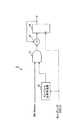
図1は本発明の一実施の形態に係るデジタルフィルタの構成図である。本実施の形態に係るデジタルフィルタ1は、サンプルの移動平均をとるSincフィルタを4段に縦接続してなるSinc4乗フィルタ11と、Sinc4乗フィルタ11の後段に接続されたタップ数がKの移動平均フィルタ12とで構成されている。本例では移動平均フィルタ12のタップ数とSincN乗フィルタの乗数とが一致しているが、後述するように所望のノッチ位置との関係で任意の数に決めればよい。デジタルフィルタ1の前段にはアナログ部2が接続されている。Hereinafter, embodiments of the present invention will be described in detail with reference to the accompanying drawings.
FIG. 1 is a block diagram of a digital filter according to an embodiment of the present invention. The
Sinc4乗フィルタ11は、それぞれがタップ数Mの移動平均フィルタからなるSincフィルタを、4段に縦接続して構成することができる。本実施の形態では、回路規模の小型化を図るため、後述するインパルス応答生成器を利用してSincフィルタを4段に縦接続したものと同等の機能を実現した回路構成を採る。 The sinc
移動平均フィルタ12は、タップ数=4となる移動平均フィルタであり、直列接続された3つの遅延要素13a、13b、13cと、入力段の遅延要素13aへの入力及び各遅延要素13a、13b、13cの出力を加算する加算器14とで構成されている。移動平均フィルタ12のタップ数は所望のノッチ位置に合わせて設定される。Sinc4乗フィルタ11に対して移動平均フィルタ12のタップ数を4とした場合には、サンプル周波数fsの1/4、1/2、3/4の位置にノッチを形成することができる。 The moving
アナログ部2は、所定のクロック数毎にアナログ演算(例えば、アナログ積分演算)してアナログ演算結果をビットデータにして出力する。本実施の形態では、4クロックで1回の積分演算を実行し、その積分演算結果はコンパレータを介して2ビットに変換して出力される。すなわち、アナログ部2の出力が変化するタイミングと、Sinc4乗フィルタ11の動作タイミング(4段構成)と、移動平均フィルタ12のタップ数(=4)との整合性が取られている。 The
本実施の形態に係るデジタルフィルタ1は、アナログ部2から出力される2値のビットストリームから所定の検出量に対応するデジタル値を出力すると共に、フィルタ機能によりノイズの抑制を図るものである。 The
図2はインパルス応答生成器を利用してデジタルフィルタ1を構成した構成例を示す図である。同図に示すデジタルフィルタ1は、インパルス応答生成器21と、インパルス応答生成器21で生成されたインパルス応答とアナログ部2から与えられるビットデータとの積を演算する積演算処理部22と、1サンプリング前の積演算結果と今回の積演算結果とを加算する加算部23と、加算部23の出力をサンプリングクロックに同期して1クロックだけ遅延させるフリップフロップ24とを備えて構成される。 FIG. 2 is a diagram illustrating a configuration example in which the
ここで、デジタルフィルタのインパルス応答はテーブル等を用いて実装することも可能であるが、長いタップ数のフィルタを実現する際には回路規模が非常に大きくなってしまう。本実施の形態に係るデジタルフィルタ1(Sinc4乗フィルタ11とタップ数4の移動平均フィルタ12との組み合わせ)のインパルス応答を3回微分すると、ある法則を持った値となることに着目し、その特性を活かしてハードウエア化することで小規模な回路を実現している。 Here, the impulse response of the digital filter can be mounted using a table or the like, but the circuit scale becomes very large when realizing a filter with a long tap number. Paying attention to the fact that when the impulse response of the digital filter 1 (combination of the Sinc
図3はインパルス応答生成器21の構成図である。3回微分生成器31は、デジタルフィルタ1のインパルス応答の3回微分値が登録された3回微分テーブル31aを有する。3回微分テーブル31aにはインデックス(0〜4M−4)に対応して3回微分値がそれぞれ設定されている。MはSincフィルタ1段当たりのタップ数である。3回微分生成器31の出力段には、3つの積分器が直列に接続されている。各積分器は、加算器(32,34,36)と遅延要素(33,35,37)で構成されている。このように、インパルス応答の3回微分値を3回積分することで元のインパルス応答を生成している。 FIG. 3 is a configuration diagram of the
図4Aは上記デジタルフィルタ1のフィルタ周波数特性を示しており、図4BはSinc4乗フィルタ11だけのフィルタ周波数特性を示している。図4A,図4Bともにサンプル周波数fsの1/2までの周波数範囲を示している。 4A shows the filter frequency characteristic of the
図4Aに示すように、本実施の形態に係るデジタルフィルタ1のフィルタ周波数特性は、サンプル周波数fsの1/4、1/2の位置にノッチが形成されている。アナログ部2がサンプル周波数fsの1/4又は1/2位置にノイズ通過帯を持つ場合には、デジタルフィルタ1において除去することができる。 As shown in FIG. 4A, the filter frequency characteristic of the
なお、Sinc4乗フィルタ11のフィルタ周波数特性は、図4Bに示すように、所要の位置(例えば、サンプル周波数fsの1/4又は1/2位置)にノッチが形成されていない。このため、デジタルフィルタ1に比べてノイズ耐性が低く、精度劣化を招く可能性がある。 As shown in FIG. 4B, the filter frequency characteristic of the sinc
次に、4クロックで1回の積分演算を実行し、その積分演算結果はコンパレータを介して2ビットに変換して出力し、サンプル周波数fsの1/2位置にノイズ通過帯を持つアナログ部2の具体例について説明する。かかるアナログ部2として、微小な静電容量の変化を検出しデジタル信号に変換して取り込む容量検出装置がある。 Next, an integration operation is performed once in 4 clocks, and the integration operation result is converted into 2 bits via a comparator and output, and the
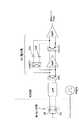
図5は容量検出装置の構成図である。この容量検出装置は、静電容量型のタッチセンサモジュールのセンサ部40に接続されているものとする。なお、本発明では、センサ部40はタッチパッドなどの入力デバイスに限定されるものではない。センサ部40は、被検出容量である容量(Cs、Cf)で構成される。一方の容量Cfは指等の接近により容量変化するが、他方の容量Csは指等の接近による容量変化を受けない。容量Cs、Cfは、スイッチSW1を介して第1の固定電圧(Vdd)と第2の固定電圧(グランド電位GND)に接続可能であると共に、クロススイッチXS1により容量Cs、Cfに対して印加する固定電圧を切り替えることができる。 FIG. 5 is a configuration diagram of the capacity detection apparatus. This capacitance detection device is assumed to be connected to the sensor unit 40 of the capacitive touch sensor module. In the present invention, the sensor unit 40 is not limited to an input device such as a touch pad. The sensor unit 40 is configured by a capacity (Cs, Cf) that is a detected capacity. One capacity Cf changes in capacity due to the approach of a finger or the like, while the other capacity Cs does not receive a capacity change due to the approach of a finger or the like. The capacitors Cs and Cf can be connected to the first fixed voltage (Vdd) and the second fixed voltage (ground potential GND) via the switch SW1, and are applied to the capacitors Cs and Cf by the cross switch XS1. The fixed voltage can be switched.
この容量検出装置は、センサ部40に接続されたチョッピングフィルタ50と、チョッピングフィルタ50の出力端に接続された積分器60とを備えて構成される。チョッピングフィルタ50は、センサ部40で検出される容量値を電荷量に変換すると共に、低周波の外来ノイズを高周波に変換する機能を有する。チョッピングフィルタ50には本来検出対象外であるセンサ容量Csをキャンセルするベース電荷量キャンセル機構を備えても良い。チョッピングフィルタ50はセンサ部40の容量Cs、Cfに対してスイッチSW2を介して接続する。また、チョッピングフィルタ50は、スイッチSW2を介して接続した容量Cs、Cfを、スイッチSW3を介して第1の固定電圧(Vdd)と第2の固定電圧(グランド電位GND)に接続可能であると共に、クロススイッチXS2により容量Cs、Cfに対して印加する固定電圧を切り替えることができる。また、チョッピングフィルタ50は、スイッチSW2を介して容量Cs、Cfに並列接続されるローパスフィルタLPFと、ローパスフィルタLPFの平衡出力を、後段の積分器60へ入力するクロススイッチXINとを備える。 The capacitance detection device includes a chopping
積分器60は、チョッピングフィルタ50から出力される電気信号(電荷量)を積分しながら指容量Cfに対応する電荷量を電圧に変換して増幅すると共に、ADコンバータ機能の一部を担うためにデルタシグマモジュレータとして機能する。積分器60は、オペアンプAMP、コンパレータCMPを備えている。オペアンプAMPの平衡出力端にクロススイッチXOUT1が接続され、クロススイッチXOUT1の出力端とオペアンプAMPの入力端との間にフィードバックコンデンサ(Cb1,Cb2)が接続されている。フィードバックコンデンサ(Cb1,Cb2)の電圧をオペアンプAMPの入力端へフィードバックする経路上にクロススイッチXOUT2が接続されている。また、オペアンプAMPの平衡出力端はクロススイッチXOUT1を介してコンパレータCMPの入力端に接続される。 The integrator 60 integrates the electric signal (charge amount) output from the chopping
以上のように構成された容量検出装置においてコンパレータCMPの出力が変化するまでの1サイクルについて説明する。 One cycle until the output of the comparator CMP changes in the capacitance detection device configured as described above will be described.
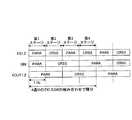
図6は、1回の積分演算が完了するまでの1サイクルにおけるクロススイッチXS1、2、XIN、XOUT1、2のパラレル接続/クロス接続について示す図である。図6に示すように、1回の積分演算動作に相当する1サイクルは、第1ステージから第4ステージで構成されており、1ステージはサンプリング周波数fsの1/fsに相当する。 FIG. 6 is a diagram illustrating the parallel connection / cross connection of the cross switches XS1, 2, XIN, XOUT1, 2 in one cycle until one integration operation is completed. As shown in FIG. 6, one cycle corresponding to one integral calculation operation is composed of the first stage to the fourth stage, and one stage corresponds to 1 / fs of the sampling frequency fs.
第1ステージは、クロススイッチXS1,2、XIN及びXOUT1,2をそれぞれパラレル接続する。その後、SW1、SW3を一定期間ONにし、SW1、SW3をOFFしたあとにSW2を一定期間ONする。その後、SW2をOFFにし、2つのCmod(SW2の右側のキャパシタ)に蓄えられた電荷の差分を積分器60に転送する The first stage connects the cross switches XS1, 2, XIN and XOUT1, 2 in parallel. Thereafter, SW1 and SW3 are turned on for a certain period, and after SW1 and SW3 are turned off, SW2 is turned on for a certain period. Thereafter, SW2 is turned OFF, and the difference between the charges stored in the two Cmods (capacitors on the right side of SW2) is transferred to the integrator 60.
第2ステージは、クロススイッチXS1,2、XINをクロス接続し、XOUT1,2をパラレル接続する。その後、SW1、SW3を一定期間ONにし、SW1、SW3をOFFしたあとにSW2を一定期間ONする。その後、SW2をOFFにし、2つのCmod(SW2の右側のキャパシタ)に蓄えられた電荷の差分を積分器60に転送する In the second stage, the cross switches XS1, 2, XIN are cross-connected, and XOUT1, 2 are connected in parallel. Thereafter, SW1 and SW3 are turned on for a certain period, and after SW1 and SW3 are turned off, SW2 is turned on for a certain period. Thereafter, SW2 is turned OFF, and the difference between the charges stored in the two Cmods (capacitors on the right side of SW2) is transferred to the integrator 60.
第3ステージは、クロススイッチXS1,2はパラレル接続し、XIN,XOUT1,2をクロス接続する。その後、SW1、SW3を一定期間ONにし、SW1、SW3をOFFしたあとにSW2を一定期間ONする。その後、SW2をOFFにし、2つのCmod(SW2の右側のキャパシタ)に蓄えられた電荷の差分を積分器60に転送する In the third stage, the cross switches XS1 and XS2 are connected in parallel, and XIN, XOUT1 and 2 are cross-connected. Thereafter, SW1 and SW3 are turned on for a certain period, and after SW1 and SW3 are turned off, SW2 is turned on for a certain period. Thereafter, SW2 is turned OFF, and the difference between the charges stored in the two Cmods (capacitors on the right side of SW2) is transferred to the integrator 60.
第4ステージは、クロススイッチXS1,2をクロス接続し、XINをパラレル接続し、XOUT1,2をクロス接続する。その後、SW1、SW3を一定期間ONにし、SW1、SW3をOFFしたあとにSW2を一定期間ONする。その後、SW2をOFFにし、2つのCmod(SW2の右側のキャパシタ)に蓄えられた電荷の差分を積分器60に転送する In the fourth stage, the cross switches XS1, 2 are cross-connected, XIN is connected in parallel, and XOUT1, 2 are cross-connected. Thereafter, SW1 and SW3 are turned on for a certain period, and after SW1 and SW3 are turned off, SW2 is turned on for a certain period. Thereafter, SW2 is turned OFF, and the difference between the charges stored in the two Cmods (capacitors on the right side of SW2) is transferred to the integrator 60.
このように、第1ステージから第4ステージを経てコンパレータCMPからアナログ積分演算結果(2ビット)が出力される。 Thus, the analog integration calculation result (2 bits) is output from the comparator CMP through the first stage through the fourth stage.
この容量検出装置によれば、クロススイッチXS1,2、XINにより前段で発生又は印加される低周波ノイズが低減される。また、XIN,XOUT1,2によりオペアンプAMPが発生する低周波ノイズ(フリッカノイズなど)が低減される。 According to this capacitance detection device, low frequency noise generated or applied in the previous stage by the cross switches XS1, 2, and XIN is reduced. Further, low frequency noise (such as flicker noise) generated by the operational amplifier AMP is reduced by XIN, XOUT1, and 2.
この容量検出装置は、デジタルフィルタ1と同じシステムクロックに同期して動作し、4クロック毎にコンパレータCMPの出力が変化する。また、コンパレータCMPの出力であるビットストリームにはサンプリング周波数fsのfs/2位置にノイズが現れる。 This capacitance detection device operates in synchronization with the same system clock as the
この容量検出装置の後段に、本実施の形態のデジタルフィルタ1を接続することにより、容量検出装置から4クロック毎に変化するビットストリームが出力され、デジタルフィルタ1では前段のSinc4乗フィルタ11での処理が4クロックで完了し、後段の移動平均フィルタ12での処理が4クロックで完了する。したがって、前段のアナログ部2となる容量検出装置でのアナログ演算動作周期と後段のデジタルフィルタ1での周期とを完全に整合することができ、効率的な演算処理を実現できる。しかも、Sinc4乗フィルタ11の後段にタップ数が4である移動平均フィルタ12を接続したことにより、アナログ部2のノイズ通過域であるサンプリング周波数fsのfs/2位置にノッチを形成でき、ノイズ減衰により検出精度を改善することができる。 By connecting the
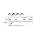
図7は他の容量検出装置の構成図である。この容量検出装置は、センサ部40の容量Cs、Cfに対してパルスを印加するように構成している。パルス発生器PGENがパルスを発生させている。 FIG. 7 is a configuration diagram of another capacity detection device. This capacitance detection device is configured to apply a pulse to the capacitances Cs and Cf of the sensor unit 40. A pulse generator PGEN generates a pulse.
図8は図7に示す容量検出装置におけるクロススイッチXIN、XOUT1,2及びパルスの組み合わせを示している。第1ステージでは、クロススイッチXINはパラレル接続、XOUT1,2はパラレル接続で、パルスは前半がローレベル、後半がハイレベルに変化している。第2ステージでは、クロススイッチXINはクロス接続、XOUT1,2はパラレル接続で、パルスは前半がハイレベル、後半がローレベルに変化している。第3ステージでは、クロススイッチXINはクロス接続、XOUT1,2はクロス接続で、パルスは前半がローレベル、後半がハイレベルに変化している。第4ステージでは、クロススイッチXINはパラレル接続、XOUT1,2はクロス接続で、パルスは前半がハイレベル、後半がローレベルに変化している。 FIG. 8 shows a combination of cross switches XIN, XOUT1, 2 and pulses in the capacitance detection device shown in FIG. In the first stage, the cross switch XIN is connected in parallel, XOUT1 and XOUT2 are connected in parallel, and the pulse changes to the low level in the first half and to the high level in the second half. In the second stage, the cross switch XIN is cross-connected, and XOUT1 and XOUT2 are connected in parallel, and the pulses change to high level in the first half and to low level in the second half. In the third stage, the cross switch XIN is cross-connected, and XOUT1 and XOUT2 are cross-connected, and the pulse changes to low level in the first half and high level in the second half. In the fourth stage, the cross switch XIN is connected in parallel, and XOUT1 and XOUT2 are cross connected, and the pulse changes to high level in the first half and to low level in the second half.
以上の第1ステージから第4ステージの1サイクルで積分器60における積分演算が1回実行される。このように、図8は示す容量検出装置においても、4クロック毎にコンパレータCMPの積分出力が変化する。 The integration calculation in the integrator 60 is executed once in one cycle from the first stage to the fourth stage. Thus, also in the capacitance detection device shown in FIG. 8, the integrated output of the comparator CMP changes every four clocks.
本発明は上記実施の形態に限定されるものではなく、本発明の要旨を逸脱しない範囲で変形実施可能である。たとえば、アナログ部2は容量検出装置に限定されるものではなく、その他の積分器であっても適用可能である。 The present invention is not limited to the above embodiment, and can be modified without departing from the gist of the present invention. For example, the
本発明は、Sincフィルタが多段に縦接続されてなるデジタルフィルタに適用可能である。 The present invention can be applied to a digital filter in which Sinc filters are vertically connected in multiple stages.
1 デジタルフィルタ
2 アナログ部
11 Sinc4乗フィルタ
12 移動平均フィルタ(4タップ)
13a、13b、13c 遅延要素
14 加算器
21 インパルス応答生成器
22 積演算処理部
23 加算部
24 フリップフロップ
31 3回微分生成器
31a 3回微分テーブル
32、34、36 加算器
33、35、37 遅延要素DESCRIPTION OF
13a, 13b,
Claims (4)
Translated fromJapaneseサンプルの移動平均をとるSincフィルタがN段に縦接続されてなるSincN乗フィルタと、前記SincN乗フィルタの出力段に接続されたKタップ数の移動平均フィルタと、を備えて構成されることを特徴とするデジタルフィルタ。A digital filter in which an analog unit that changes the bit data output of an analog operation result every N clocks is arranged in the preceding stage, operates with a clock synchronized with the analog unit, and removes noise from the bit data output from the analog unit Because
A Sinc filter that takes a moving average of samples is configured to include a SincN power filter that is vertically connected in N stages, and a moving average filter with the number of K taps that is connected to the output stage of the SincN power filter. Features digital filter.
前記移動平均フィルタは、タップ数が4の移動平均フィルタで構成され、
前記アナログ部は、前記アナログ演算として積分を1回4クロックで行い、サンプリング周波数fsに対してfs/2にノイズ通過域を持つ、
ことを特徴とする請求項1から請求項3のいずれかに記載のデジタルフィルタ。The SincN power filter is configured by vertically connecting Sinc filters with M taps in four stages,
The moving average filter is composed of a moving average filter having 4 taps,
The analog unit performs integration once in 4 clocks as the analog operation, and has a noise pass band at fs / 2 with respect to the sampling frequency fs.
The digital filter according to any one of claims 1 to 3, wherein the digital filter is provided.
Priority Applications (3)
| Application Number | Priority Date | Filing Date | Title |
|---|---|---|---|
| JP2010133039AJP2011259293A (en) | 2010-06-10 | 2010-06-10 | Digital filter |
| CN2011101489007ACN102332894A (en) | 2010-06-10 | 2011-06-03 | Digital filter |
| US13/154,281US20110307536A1 (en) | 2010-06-10 | 2011-06-06 | Digital filter |
Applications Claiming Priority (1)
| Application Number | Priority Date | Filing Date | Title |
|---|---|---|---|
| JP2010133039AJP2011259293A (en) | 2010-06-10 | 2010-06-10 | Digital filter |
Publications (1)
| Publication Number | Publication Date |
|---|---|
| JP2011259293Atrue JP2011259293A (en) | 2011-12-22 |
Family
ID=45097122
Family Applications (1)
| Application Number | Title | Priority Date | Filing Date |
|---|---|---|---|
| JP2010133039AWithdrawnJP2011259293A (en) | 2010-06-10 | 2010-06-10 | Digital filter |
Country Status (3)
| Country | Link |
|---|---|
| US (1) | US20110307536A1 (en) |
| JP (1) | JP2011259293A (en) |
| CN (1) | CN102332894A (en) |
Cited By (4)
| Publication number | Priority date | Publication date | Assignee | Title |
|---|---|---|---|---|
| US8510589B2 (en)* | 2008-08-29 | 2013-08-13 | Intel Mobile Communications GmbH | Apparatus and method using first and second clocks |
| CN103281053A (en)* | 2013-05-02 | 2013-09-04 | 天津大学 | Quick response digital decimation filter |
| KR20130112792A (en)* | 2012-04-04 | 2013-10-14 | 페어차일드 세미컨덕터 코포레이션 | Noise reduction method with chopping for a merged mems accelerometer sensor |
| KR101877622B1 (en)* | 2016-09-07 | 2018-07-11 | 주식회사 한화 | Variable window based filter and method for operating the same |
Families Citing this family (15)
| Publication number | Priority date | Publication date | Assignee | Title |
|---|---|---|---|---|
| CN103221778B (en) | 2010-09-18 | 2016-03-30 | 快捷半导体公司 | There is single micromechanics one chip three-axis gyroscope driven |
| WO2012037536A2 (en) | 2010-09-18 | 2012-03-22 | Fairchild Semiconductor Corporation | Packaging to reduce stress on microelectromechanical systems |
| WO2012040211A2 (en) | 2010-09-20 | 2012-03-29 | Fairchild Semiconductor Corporation | Microelectromechanical pressure sensor including reference capacitor |
| US8978475B2 (en) | 2012-02-01 | 2015-03-17 | Fairchild Semiconductor Corporation | MEMS proof mass with split z-axis portions |
| US9488693B2 (en) | 2012-04-04 | 2016-11-08 | Fairchild Semiconductor Corporation | Self test of MEMS accelerometer with ASICS integrated capacitors |
| EP2647952B1 (en) | 2012-04-05 | 2017-11-15 | Fairchild Semiconductor Corporation | Mems device automatic-gain control loop for mechanical amplitude drive |
| KR102058489B1 (en) | 2012-04-05 | 2019-12-23 | 페어차일드 세미컨덕터 코포레이션 | Mems device front-end charge amplifier |
| EP2647955B8 (en) | 2012-04-05 | 2018-12-19 | Fairchild Semiconductor Corporation | MEMS device quadrature phase shift cancellation |
| US9625272B2 (en) | 2012-04-12 | 2017-04-18 | Fairchild Semiconductor Corporation | MEMS quadrature cancellation and signal demodulation |
| DE102013014881B4 (en) | 2012-09-12 | 2023-05-04 | Fairchild Semiconductor Corporation | Enhanced silicon via with multi-material fill |
| CN103001606A (en)* | 2012-11-14 | 2013-03-27 | 无锡商业职业技术学院 | digital filter |
| US9835647B2 (en) | 2014-03-18 | 2017-12-05 | Fairchild Semiconductor Corporation | Apparatus and method for extending analog front end sense range of a high-Q MEMS sensor |
| US9864455B2 (en) | 2015-05-29 | 2018-01-09 | Synaptics Incorporated | Matched filter for a first order sigma delta capacitance measurement system and a method to determine the same |
| CN105306007A (en)* | 2015-10-30 | 2016-02-03 | 无锡纳讯微电子有限公司 | Digital filter |
| US12360176B2 (en)* | 2023-09-13 | 2025-07-15 | Legrand DPC, LLC | Residual current monitor |
Family Cites Families (7)
| Publication number | Priority date | Publication date | Assignee | Title |
|---|---|---|---|---|
| JP3771195B2 (en)* | 2002-05-17 | 2006-04-26 | 株式会社イシダ | Weight measuring noise removing device and weight measuring noise removing method |
| US6774822B1 (en)* | 2003-01-09 | 2004-08-10 | Process Control Corporation | Method and systems for filtering unwanted noise in a material metering machine |
| US6968296B2 (en)* | 2003-04-04 | 2005-11-22 | Radiodetection Limited | Cable detector with decimating filter and filtering method |
| JP4197293B2 (en)* | 2003-12-10 | 2008-12-17 | パナソニック株式会社 | A / D converter, D / A converter |
| JP5054324B2 (en)* | 2006-04-19 | 2012-10-24 | 沖電気工業株式会社 | Noise reduction device for voice communication terminal |
| JP2007324659A (en)* | 2006-05-30 | 2007-12-13 | Sony Corp | Charged main filter circuit |
| JP4296518B2 (en)* | 2006-12-07 | 2009-07-15 | ソニー株式会社 | Information processing apparatus and information processing method |
- 2010
- 2010-06-10JPJP2010133039Apatent/JP2011259293A/ennot_activeWithdrawn
- 2011
- 2011-06-03CNCN2011101489007Apatent/CN102332894A/enactivePending
- 2011-06-06USUS13/154,281patent/US20110307536A1/ennot_activeAbandoned
Cited By (5)
| Publication number | Priority date | Publication date | Assignee | Title |
|---|---|---|---|---|
| US8510589B2 (en)* | 2008-08-29 | 2013-08-13 | Intel Mobile Communications GmbH | Apparatus and method using first and second clocks |
| KR20130112792A (en)* | 2012-04-04 | 2013-10-14 | 페어차일드 세미컨덕터 코포레이션 | Noise reduction method with chopping for a merged mems accelerometer sensor |
| KR102045784B1 (en)* | 2012-04-04 | 2019-11-18 | 페어차일드 세미컨덕터 코포레이션 | Noise reduction method with chopping for a merged mems accelerometer sensor |
| CN103281053A (en)* | 2013-05-02 | 2013-09-04 | 天津大学 | Quick response digital decimation filter |
| KR101877622B1 (en)* | 2016-09-07 | 2018-07-11 | 주식회사 한화 | Variable window based filter and method for operating the same |
Also Published As
| Publication number | Publication date |
|---|---|
| CN102332894A (en) | 2012-01-25 |
| US20110307536A1 (en) | 2011-12-15 |
Similar Documents
| Publication | Publication Date | Title |
|---|---|---|
| JP2011259293A (en) | Digital filter | |
| CN103840778B (en) | Amplifier apparatus and method with filtering | |
| CN111988038A (en) | VCO-Based Continuous-Time Pipelined ADC | |
| KR20130142952A (en) | System and method for chopping oversampled data converters | |
| WO2007072712A4 (en) | Sampling filter device | |
| US8779958B1 (en) | Continuous time input stage | |
| CN105917578A (en) | Circuits and methods for switch-mode operational amplifiers | |
| US10101709B2 (en) | Time register | |
| US20140159929A1 (en) | Delta-modulation signal processors: linear, nonlinear and mixed | |
| CN111817716B (en) | High efficiency Voltage Controlled Oscillator (VCO) analog to digital converter (ADC) | |
| KR20210015675A (en) | Voltage controlled oscillator based analog-to-digital converter including a maximum length sequence generator | |
| Ziabakhsh et al. | A Second-Order Bandpass $\Delta\Sigma $ Time-to-Digital Converter With Negative Time-Mode Feedback | |
| JP2016015132A (en) | Touch detection device and touch detection method | |
| US20220052707A1 (en) | Analog front-end circuit capable of use in a sensor system | |
| Sun et al. | A 951-fs rms period jitter 3.2% modulation range in-band modulation spread-spectrum clock generator | |
| US9973171B2 (en) | Digital filter | |
| JP2014052282A (en) | Frequency measurement circuit | |
| US20130271210A1 (en) | N-path filter with coupling between paths | |
| US9319060B2 (en) | Frequency response compensation in a digital to analog converter | |
| US6473011B1 (en) | Serial D/A converter compensating for capacitor mismatch errors | |
| US20190128710A1 (en) | Sensor signal detection apparatus | |
| Abdelfattah et al. | Cascade and LC ladder-based filter realizations using synchronous time-mode signal processing | |
| TW201535968A (en) | Synchronous charge sharing filter | |
| JP6371646B2 (en) | Feedback type pulse width modulator | |
| CN105306007A (en) | Digital filter |
Legal Events
| Date | Code | Title | Description |
|---|---|---|---|
| A300 | Application deemed to be withdrawn because no request for examination was validly filed | Free format text:JAPANESE INTERMEDIATE CODE: A300 Effective date:20130903 |