JP2011259191A - Δς modulator - Google Patents
Δς modulatorDownload PDFInfo
- Publication number
- JP2011259191A JP2011259191AJP2010131679AJP2010131679AJP2011259191AJP 2011259191 AJP2011259191 AJP 2011259191AJP 2010131679 AJP2010131679 AJP 2010131679AJP 2010131679 AJP2010131679 AJP 2010131679AJP 2011259191 AJP2011259191 AJP 2011259191A
- Authority
- JP
- Japan
- Prior art keywords
- modulator
- integrator
- output
- signal
- quantizer
- Prior art date
- Legal status (The legal status is an assumption and is not a legal conclusion. Google has not performed a legal analysis and makes no representation as to the accuracy of the status listed.)
- Pending
Links
- 238000006243chemical reactionMethods0.000claimsabstractdescription9
- 238000005070samplingMethods0.000claimsdescription80
- 230000010354integrationEffects0.000claimsdescription30
- 238000000034methodMethods0.000claimsdescription13
- 230000008569processEffects0.000claimsdescription9
- 230000001360synchronised effectEffects0.000claimsdescription6
- 238000013139quantizationMethods0.000abstractdescription20
- 239000003990capacitorSubstances0.000description124
- 229920005994diacetyl cellulosePolymers0.000description8
- 238000010586diagramMethods0.000description8
- 238000007493shaping processMethods0.000description4
- 230000009471actionEffects0.000description3
- 230000000694effectsEffects0.000description2
- 230000002708enhancing effectEffects0.000description2
- 230000002238attenuated effectEffects0.000description1
- 230000007423decreaseEffects0.000description1
- 238000005516engineering processMethods0.000description1
- 230000006872improvementEffects0.000description1
- 230000009467reductionEffects0.000description1
- 230000004044responseEffects0.000description1
Images


Landscapes
- Compression, Expansion, Code Conversion, And Decoders (AREA)
Abstract
Description
Translated fromJapanese本発明は、AD変換器に適用されるΔΣ変調器に関し、より詳細には、複数チャネルのアナログ入力を処理する機能を有しAD変換器を構成するに適合したΔΣ変調器に関する。 The present invention relates to a delta-sigma modulator applied to an AD converter, and more particularly to a delta-sigma modulator that has a function of processing analog inputs of a plurality of channels and is suitable for constituting an AD converter.
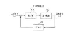
一般的にオーバサンプルAD変換器の基本回路方式であるΔΣ変調器は、図4の機能ブロック図に示すような構成を採る。即ち、このΔΣ変調器400は、フォワード経路の積分器410、フィードバックループの量子化器420、および、DAC(デジタルアナログ変換器)430を含んで構成される。
ΔΣ変調器400の出力部である量子化器420の出力信号は、入力信号と量子化ノイズとの和を含んだ量子化信号(小ビットのデジタル信号)である。
この量子化ノイズは、連続的なアナログ信号を離散的なデジタル信号に変換する際に必然的に生じる誤差成分である。In general, a delta-sigma modulator, which is a basic circuit system of an oversampled AD converter, has a configuration as shown in a functional block diagram of FIG. That is, the ΔΣ modulator 400 includes a
The output signal of the
This quantization noise is an error component that inevitably occurs when a continuous analog signal is converted into a discrete digital signal.
量子化ノイズは、ΔΣ変調器が有するノイズシェーピングの作用によって、高域側にシフトされ、信号帯域内では減衰される。従って、ノイズシェーピングの作用を高めることによってS/N特性の改善を期待することができる。そして、ノイズシェーピングの作用を高めるための最も有効な手段は、積分器の次数を増やすことであり、1次数増加に対してオーバサンプル比の2乗に逆比例した量子化ノイズが減少される。
尚、積分器の次数を3次以上にする場合は、高次ループの安定性を考慮して、マルチビット量子化器で構成することになる。The quantization noise is shifted to the high frequency side by the action of noise shaping included in the ΔΣ modulator, and is attenuated within the signal band. Therefore, improvement of the S / N characteristic can be expected by enhancing the action of noise shaping. The most effective means for enhancing the noise shaping action is to increase the order of the integrator, and the quantization noise that is inversely proportional to the square of the oversample ratio with respect to the increase in the first order is reduced.
When the order of the integrator is set to the third order or higher, the multi-bit quantizer is configured in consideration of the stability of the higher-order loop.
マルチビット量子化器で構成したΔΣ変調器は、高次ノイズシェーピングの作用に加えて、量子化器の分解能が1ビット増すごとに量子化ノイズが6dB減少する特徴と、量子化器出力の変調器入力信号に対する追従性が向上し、変調器入力信号とDAC出力信号との差が小さくなるために積分器の消費電流が削減できるという特徴がある。
その反面、マルチビット量子化器は、一般的にFLASH型ADC(アナログデジタル変換器)で構成されるため、ビット数に応じて回路規模が大きくなることと、それに付随して消費電流が増加するといった課題がある。
また、上述のようなΔΣ変調器では、1つのΔΣ変調器は、1チャネルの入力信号のみを処理するため、複数チャネルの入力信号を処理するためには、チャネル数に応じたΔΣ変調器を並設する必要があった。In addition to the effect of higher-order noise shaping, the ΔΣ modulator composed of multi-bit quantizers has a feature that the quantization noise decreases by 6 dB every time the resolution of the quantizer increases by 1 bit, and modulation of the quantizer output. The followability with respect to the modulator input signal is improved, and the difference between the modulator input signal and the DAC output signal is reduced, so that the current consumption of the integrator can be reduced.
On the other hand, since the multi-bit quantizer is generally composed of a FLASH ADC (analog-digital converter), the circuit scale increases with the number of bits, and the current consumption increases accordingly. There is a problem.
Further, in the above-described ΔΣ modulator, since one ΔΣ modulator processes only one channel input signal, a ΔΣ modulator corresponding to the number of channels is used to process a plurality of channel input signals. It was necessary to install them side by side.
図5は、従来の2チャネルADCにおける、第1ΔΣ変調器と第2ΔΣ変調器とを併設した具体的な回路例を表す回路図である。
図5の2チャネルADC500における、第1ΔΣ変調器510および第2ΔΣ変調器520は、図4を参照して説明したΔΣ変調器の構成を具体的に示したものである。
第1ΔΣ変調器510は、フォワード経路の入力信号サンプリング回路511、積分器512を有し、更に、フィードバックループの量子化器513およびDAC514を含んで構成される。サンプリング回路511は、図示のように、アナログスイッチSW101〜SW104を有する。そして、第1ΔΣ変調器510は、入力信号Aに対して量子化信号Qaを得る。FIG. 5 is a circuit diagram showing a specific circuit example in which a first ΔΣ modulator and a second ΔΣ modulator are provided side by side in a conventional 2-channel ADC.
The first ΔΣ modulator 510 and the second ΔΣ modulator 520 in the two-channel ADC 500 of FIG. 5 specifically show the configuration of the ΔΣ modulator described with reference to FIG.
The first ΔΣ modulator 510 includes a forward path input signal sampling circuit 511 and an integrator 512, and further includes a
第2ΔΣ変調器520は、同様に、フォワード経路の入力信号サンプリング回路521、積分器522を有し、更に、フィードバックループの量子化器523およびDAC524を含んで構成される。サンプリング回路521は、図示のように、アナログスイッチSW201〜SW204を有する。そして、第2ΔΣ変調器520は、入力信号Bに対して量子化信号Qbを得る。
尚、図5における各量子化器510および520、ならびに、DAC514および524は、それぞれ1ビット構成であるが、これらはNビット以上のマルチビット構成を採り得る。
図5の2チャネルADC500における、第1ΔΣ変調器510(第2ΔΣ変調器520)の構成の細部については、次の図6を併せ参照して詳述する。Similarly, the second ΔΣ modulator 520 includes a forward path input signal sampling circuit 521 and an integrator 522, and further includes a
Note that each of the quantizers 510 and 520 and the DACs 514 and 524 in FIG. 5 have a 1-bit configuration, but these may have a multi-bit configuration of N bits or more.
Details of the configuration of the first ΔΣ modulator 510 (second ΔΣ modulator 520) in the 2-channel ADC 500 of FIG. 5 will be described in detail with reference to FIG.
図6は、図5の2チャネルADCの動作を表すタイミングチャートである。この図6には、第1ΔΣ変調器510および第2ΔΣ変調器520双方の動作が表されている。本例の場合これら双方の動作は同様である。このため、以下には、第1ΔΣ変調器510についてのみ詳述し、ここから容易に理解される第2ΔΣ変調器520に関する説明は第1ΔΣ変調器510に関する説明を援用してこれに替える。 FIG. 6 is a timing chart showing the operation of the 2-channel ADC of FIG. FIG. 6 shows the operations of both the first ΔΣ modulator 510 and the second ΔΣ modulator 520. In this example, both operations are the same. Therefore, only the first ΔΣ modulator 510 will be described in detail below, and the description regarding the second ΔΣ modulator 520 that can be easily understood from here will be replaced with the description regarding the first ΔΣ modulator 510.
このタイミングチャートに表された各部は、既述のアナログスイッチSW101〜SW104およびアナログスイッチSW201〜SW204を駆動する制御信号φによって各動作タイミングが制御される。
図6における入力信号AはA1、A1′、A2、A2′、A3・・・の順に入力される。また、入力信号BはB1、B1′、B2、B2′、B3・・・の順に入力される。Each unit shown in this timing chart has its operation timing controlled by the control signal φ that drives the analog switches SW101 to SW104 and the analog switches SW201 to SW204 described above.
The input signal A in FIG. 6 is input in the order of A1, A1 ′, A2, A2 ′, A3. The input signal B is inputted in the order of B1, B1 ′, B2, B2 ′, B3.
第1ΔΣ変調器510の入力信号サンプリング回路511では、アナログスイッチSW101、キャパシタC10、および、アナログスイッチSW104が上述の順に直列接続され、更に、このキャパシタC10の入力側端部と接地点との間にアナログスイッチSW102が設けられ、且つ、キャパシタC10の出力側端部と接地点との間にアナログスイッチSW103が設けられておいる。そして、これら各アナログスイッチSW101〜SW104とキャパシタC10とによってスイッチトキャパシタ回路が構成されている。 In the input signal sampling circuit 511 of the first ΔΣ modulator 510, the analog switch SW101, the capacitor C10, and the analog switch SW104 are connected in series in the order described above, and further, between the input side end of the capacitor C10 and the ground point. An analog switch SW102 is provided, and an analog switch SW103 is provided between the output side end of the capacitor C10 and the ground point. The analog switches SW101 to SW104 and the capacitor C10 constitute a switched capacitor circuit.
以上の構成において、アナログスイッチ制御信号φがHレベルのとき、アナログスイッチSW101とSW103とが導通状態となり、アナログスイッチSW102とSW104とが非導通状態となる。この状態で、キャパシタC10に入力信号Aによる電荷を充電するサンプリング動作が行われる。
次にアナログスイッチ制御信号φがLレベルのとき、入力信号サンプリング回路511のアナログスイッチSW101とSW103とが非導通状態となり、アナログスイッチSW102とSW104とが導通状態となる。この状態で、キャパシタC10に充電されていた電荷は、積分器512のオペアンプOP1に図示の如く接続されたコンデンサC13に転送される。即ち、この状態で積分動作が行われる。In the above configuration, when the analog switch control signal φ is at the H level, the analog switches SW101 and SW103 are turned on, and the analog switches SW102 and SW104 are turned off. In this state, a sampling operation is performed in which the capacitor C10 is charged with the charge due to the input signal A.
Next, when the analog switch control signal φ is at L level, the analog switches SW101 and SW103 of the input signal sampling circuit 511 are turned off and the analog switches SW102 and SW104 are turned on. In this state, the charge charged in the capacitor C10 is transferred to the capacitor C13 connected to the operational amplifier OP1 of the integrator 512 as shown in the figure. That is, the integration operation is performed in this state.
第1ΔΣ変調器510の積分器512は、オペアンプOP1の反転入力端と非反転入力端がそれぞれ加算点及び接地点に接続されており、加算点とオペアンプOP1の出力端との間には積分キャパシタC13が接続されている。
この積分器512は、アナログスイッチ制御信号φがLレベルのときに積分状態となり、サンプリング回路511およびDAC514から転送される電荷を積分して出力する。また、アナログスイッチ制御信号φがHレベルのときにホールド状態となり、積分キャパシタC13に蓄積された電荷を保持して出力する。The integrator 512 of the first ΔΣ modulator 510 has an inverting input terminal and a non-inverting input terminal of the operational amplifier OP1 connected to an addition point and a ground point, respectively, and an integration capacitor between the addition point and the output terminal of the operational amplifier OP1. C13 is connected.
The integrator 512 is in an integrated state when the analog switch control signal φ is at the L level, and integrates and outputs the charges transferred from the sampling circuit 511 and the DAC 514. When the analog switch control signal φ is at the H level, the hold state is entered, and the charge accumulated in the integration capacitor C13 is held and output.
第1ΔΣ変調器の量子化器513は、例えばFLASH型ADC(アナログデジタル変換器)であり、積分器512の出力の正負を判定する。尚、量子化器513は、Nビット量子化器として、積分器512の出力をNビットの量子化信号に変換し出力するように構成され得る。
第1ΔΣ変調器のDAC514は、量子化器513の量子化出力をDA変換するように動作する。
このDAC514では、入力信号サンプリング回路511の出力端部と第1基準電位+Vとの間に、アナログスイッチSW111、キャパシタC11、および、アナログスイッチSW114が上述の順に直列接続されている。更に、キャパシタC11のアナログスイッチSW111側の端部と接地点との間、および、キャパシタC11のアナログスイッチSW114側の端部と接地点との間に、それぞれ、アナログスイッチSW112およびSW113が設けられている。そして、これらアナログスイッチSW111〜SW114、および、キャパシタC11によって、スイッチトキャパシタ回路が構成されている。The
The DAC 514 of the first ΔΣ modulator operates to DA convert the quantized output of the
In the DAC 514, the analog switch SW111, the capacitor C11, and the analog switch SW114 are connected in series in the order described above between the output end of the input signal sampling circuit 511 and the first reference potential + V. Further, analog switches SW112 and SW113 are provided between the end of the capacitor C11 on the analog switch SW111 side and the ground point, and between the end of the capacitor C11 on the analog switch SW114 side and the ground point, respectively. Yes. The analog switches SW111 to SW114 and the capacitor C11 constitute a switched capacitor circuit.
また、入力信号サンプリング回路511の出力端部と第2基準電位−Vとの間に、アナログスイッチSW121、キャパシタC12、および、SW124が上述の順に直列接続されている。更に、キャパシタC12のアナログスイッチSW121側の端部と接地点との間、および、キャパシタC12のアナログスイッチSW124側の端部と接地点との間に、それぞれ、アナログスイッチSW122およびSW123が設けられている。
そして、これらアナログスイッチSW121〜SW124、および、キャパシタC12によってスイッチトキャパシタ回路が構成されている。
更に、上述の両スイッチトキャパシタ回路におけるアナログスイッチSW111〜SW114、および、アナログスイッチSW121〜SW124を制御するスイッチ制御回路515が設けられている。Further, the analog switch SW121, the capacitor C12, and the SW124 are connected in series in the order described above between the output end of the input signal sampling circuit 511 and the second reference potential −V. Further, analog switches SW122 and SW123 are provided between the end of the capacitor C12 on the analog switch SW121 side and the ground point, and between the end of the capacitor C12 on the analog switch SW124 side and the ground point, respectively. Yes.
The analog switches SW121 to SW124 and the capacitor C12 constitute a switched capacitor circuit.
Furthermore, a
上述の構成において、アナログスイッチ制御信号φがHレベルのときには、アナログスイッチSW111とアナログスイッチSW113、および、アナログスイッチSW121とアナログスイッチSW123は導通状態となる。同時に、アナログスイッチSW112とアナログスイッチSW114、および、アナログスイッチSW122とアナログスイッチSW124は非導通状態となる。そして、このときには、キャパシタC11に第1基準電位+Vによる電荷が蓄積され、同時に、キャパシタC12に第2基準電位−Vによる電荷が蓄積されるサンプリング動作が行われる。 In the above configuration, when the analog switch control signal φ is at the H level, the analog switch SW111 and the analog switch SW113, and the analog switch SW121 and the analog switch SW123 are in a conductive state. At the same time, the analog switch SW112 and the analog switch SW114, and the analog switch SW122 and the analog switch SW124 are turned off. At this time, a sampling operation is performed in which charges due to the first reference potential + V are accumulated in the capacitor C11, and at the same time, charges due to the second reference potential -V are accumulated in the capacitor C12.
尚、DAC514はNビットDACとして、積分器512の出力に応じたNビット量子化器の量子化出力を、キャパシタC11、C12で積分しDA変換出力を得るように構成され得る。
既述のように、第1ΔΣ変調器510および第2ΔΣ変調器520は、それらの構成および作用について同様である。
即ち、第1ΔΣ変調器510における各アナログスイッチSW101〜SW104、アナログスイッチSW111〜SW114、および、アナログスイッチSW121〜SW124に各対応して、第2ΔΣ変調器520では、各アナログスイッチSW201〜SW204、アナログスイッチSW211〜SW214、および、アナログスイッチSW221〜SW224が設けられている。Note that the DAC 514 can be configured as an N-bit DAC by integrating the quantized output of the N-bit quantizer corresponding to the output of the integrator 512 with the capacitors C11 and C12 to obtain a DA conversion output.
As described above, the first ΔΣ modulator 510 and the second ΔΣ modulator 520 have the same configuration and operation.
That is, corresponding to each analog switch SW101 to SW104, analog switch SW111 to SW114, and analog switch SW121 to SW124 in the first ΔΣ modulator 510, in the second ΔΣ modulator 520, each analog switch SW201 to SW204, analog switch SW211 to SW214 and analog switches SW221 to SW224 are provided.
また、第1ΔΣ変調器510における各キャパシタC10〜C13に対応して、第2ΔΣ変調器520では、各キャパシタC20〜C23が設けられている。
そして、上述のような各符号の割り当ては、図5および図6について同様である。
図6のタイミングチャートにおける時間区間(a)において、アナログスイッチ制御信号φがHレベルであり、第1ΔΣ変調器510の入力信号サンプリング回路511はキャパシタC10に入力信号Aの時間区間(a)の部分A1による電荷をサンプルする。Corresponding to the capacitors C10 to C13 in the first ΔΣ modulator 510, the second ΔΣ modulator 520 is provided with capacitors C20 to C23.
The assignment of each code as described above is the same as in FIGS.
In the time interval (a) in the timing chart of FIG. 6, the analog switch control signal φ is at the H level, and the input signal sampling circuit 511 of the first ΔΣ modulator 510 is connected to the capacitor C10 in the time interval (a) portion of the input signal A. Sample the charge due to A1.
また、第2ΔΣ変調器520の入力信号サンプリング回路521はキャパシタC20に入力信号Bの時間区間(a)の部分B1による電荷をサンプルする。
次に、時間区間(b)において、アナログスイッチ制御信号φがLレベルであり、第1ΔΣ変調器510の入力信号サンプリング回路511のキャパシタC10にサンプルされ入力信号Aの時間区間(a)の部分A1の電荷が、積分器512のキャパシタC13に転送され積分される。量子化器513は、積分器512の出力を量子化信号に変換し、出力する。In addition, the input signal sampling circuit 521 of the second ΔΣ modulator 520 samples the charge due to the portion B1 of the time interval (a) of the input signal B in the capacitor C20.
Next, in the time interval (b), the analog switch control signal φ is at the L level and is sampled by the capacitor C10 of the input signal sampling circuit 511 of the first ΔΣ modulator 510, and the portion A1 of the time interval (a) of the input signal A Are transferred to the capacitor C13 of the integrator 512 and integrated. The
また、第2ΔΣ変調器520の入力信号サンプリング回路2のキャパシタC20にサンプルされた入力信号B1よる電荷が、積分器522のキャパシタC23に転送され積分される。量子化器523は、積分器522の出力を量子化信号に変換し出力する。
次に、時間区間(c)において、アナログスイッチ制御信号φがHレベルであり、第1ΔΣ変調器510の入力信号サンプリング回路511はキャパシタC10に入力信号A2による電荷をサンプルする。Further, the charge due to the input signal B1 sampled in the capacitor C20 of the input signal sampling circuit 2 of the second ΔΣ modulator 520 is transferred to the capacitor C23 of the integrator 522 and integrated. The
Next, in the time interval (c), the analog switch control signal φ is at the H level, and the input signal sampling circuit 511 of the first ΔΣ modulator 510 samples the charge due to the input signal A2 in the capacitor C10.
DAC514の2つのサンプリング回路は、それぞれキャパシタC11に第1基準電位+Vによる電荷を、キャパシタC12に第2基準電位−Vによる電荷をサンプルする。
積分器512は、前フェーズである時間区間(b)の積分結果を積分器のキャパシタC13にホールドしている。そして、量子化器513は、時間区間(b)の量子化器513の出力と同じ量子化信号を出力する。The two sampling circuits of the DAC 514 respectively sample the charge based on the first reference potential + V on the capacitor C11 and the charge based on the second reference potential −V on the capacitor C12.
The integrator 512 holds the integration result of the time period (b), which is the previous phase, in the capacitor C13 of the integrator. Then, the
一方、時間区間(c)において、第2のΔΣ変調器520の入力信号サンプリング回路521はキャパシタC20に入力信号Bの時間区間(c)の部分B2による電荷をサンプルする。
DAC524の2つのサンプリング回路は、それぞれキャパシタC21に第1基準電位+Vによる電荷を、キャパシタC22に第2基準電位−Vによる電荷をサンプルする。
積分器522は、前フェーズの積分結果をそのキャパシタC23にホールドしており、量子化器523は、時間区間(b)における量子化器523の出力と同じ量子化信号を出力する。On the other hand, in the time interval (c), the input signal sampling circuit 521 of the second ΔΣ modulator 520 samples the charge due to the portion B2 of the time interval (c) of the input signal B in the capacitor C20.
The two sampling circuits of the DAC 524 sample the charge based on the first reference potential + V on the capacitor C21 and the charge based on the second reference potential −V on the capacitor C22, respectively.
The integrator 522 holds the integration result of the previous phase in the capacitor C23, and the
次に、時間区間(d)において、アナログスイッチ制御信号φがLレベルであり、第1ΔΣ変調器510の入力信号サンプリング回路511のキャパシタC10にサンプルされた入力信号Aの時間区間(c)の部分A2による電荷が、積分器512のキャパシタC13に転送され積分される。
DAC514の2つのサンプリング回路のそれぞれのキャパシタC11にサンプルされた第1基準電位+Vによる電荷と、C12にサンプルされた第2基準電位−Vによる電荷の何れかが、スイッチ制御回路515で選択され、積分器512のキャパシタC13に転送され積分される。
量子化器513は、積分器512の出力を量子化信号に変換し、出力する。Next, in the time interval (d), the analog switch control signal φ is at the L level, and the portion of the time interval (c) of the input signal A sampled in the capacitor C10 of the input signal sampling circuit 511 of the first ΔΣ modulator 510 The electric charge by A2 is transferred to the capacitor C13 of the integrator 512 and integrated.
Either the charge based on the first reference potential + V sampled in the respective capacitors C11 of the two sampling circuits of the DAC 514 or the charge based on the second reference potential −V sampled on the C12 is selected by the
The
一方、時間区間(d)において、第2のΔΣ変調器520の入力信号サンプリング回路521のキャパシタC20にサンプルされた入力信号Bの時間区間(c)の部分B2による電荷が、積分器522のキャパシタC23に転送され積分される。
DAC524の2つのサンプリング回路のそれぞれのキャパシタC21にサンプルされた第1基準電位+Vによる電荷と、C22にサンプルされた第2基準電位−Vによる電荷の何れかが、スイッチ制御回路525で選択され、積分器522のキャパシタC23に転送され積分される。On the other hand, in the time interval (d), the charge due to the portion B2 of the time interval (c) of the input signal B sampled by the capacitor C20 of the input signal sampling circuit 521 of the second ΔΣ modulator 520 becomes the capacitor of the integrator 522. It is transferred to C23 and integrated.
Either the charge based on the first reference potential + V sampled in the respective capacitors C21 of the two sampling circuits of the DAC 524 or the charge based on the second reference potential −V sampled on the C22 is selected by the
量子化器523は、積分器522の出力を量子化信号に変換し、出力する。
次に、時間区間(e)において、アナログスイッチ制御信号φがHレベルであり、第1ΔΣ変調器510の入力信号サンプリング回路511はキャパシタC10に入力信号Aの時間区間(e)の部分A3による電荷をサンプルする。
DAC514の2つのサンプリング回路は、それぞれキャパシタC11に第1基準電位+Vによる電荷を、キャパシタC12に第2基準電位−Vによる電荷をサンプルする。The
Next, in the time interval (e), the analog switch control signal φ is at the H level, and the input signal sampling circuit 511 of the first ΔΣ modulator 510 charges the capacitor C10 with the charge due to the portion A3 of the time interval (e) of the input signal A. To sample.
The two sampling circuits of the DAC 514 respectively sample the charge based on the first reference potential + V on the capacitor C11 and the charge based on the second reference potential −V on the capacitor C12.
積分器512は、前フェーズである時間区間(c)の積分結果を積分器のキャパシタC13にホールドしており、量子化器513の出力は、時間区間(d)の量子化器513の出力と同じ量子化信号を出力する。
一方、第2ΔΣ変調器520の入力信号サンプリング回路521はキャパシタC20に入力信号B3による電荷をサンプルする。
DAC524の2つのサンプリング回路は、それぞれキャパシタC21に第1基準電位+Vによる電荷を、キャパシタC22に第2基準電位−Vによる電荷をサンプルする。
積分器522は、前フェーズの積分結果B2を積分器のキャパシタC23にホールドしており、量子化器523の出力は、時間区間(d)の量子化器523の出力と同じ量子化信号を出力する。The integrator 512 holds the integration result in the time interval (c), which is the previous phase, in the capacitor C13 of the integrator, and the output of the
On the other hand, the input signal sampling circuit 521 of the second ΔΣ modulator 520 samples the charge of the input signal B3 in the capacitor C20.
The two sampling circuits of the DAC 524 sample the charge based on the first reference potential + V on the capacitor C21 and the charge based on the second reference potential −V on the capacitor C22, respectively.
The integrator 522 holds the integration result B2 of the previous phase in the capacitor C23 of the integrator, and the output of the
そして、以上説明した各回路が平衡状態に達したとき、既述の時間区間(c)〜(f)における動作を上述の順に繰り返す。
図5の従来の2チャネルADCにおけるように、第1ΔΣ変調器と第2ΔΣ変調器とをそれぞれ独立に設置した場合、チャネル数を増やすと、これに応じてΔΣ変調器の面積は略比例的に増大することになる。従って、チャネル数を増やすと、LSI上に占めるΔΣ変調器の面積が略比例的に大型化してしまうという不都合があった。When the circuits described above reach an equilibrium state, the operations in the time intervals (c) to (f) described above are repeated in the order described above.
When the first ΔΣ modulator and the second ΔΣ modulator are installed independently as in the conventional 2-channel ADC of FIG. 5, when the number of channels is increased, the area of the ΔΣ modulator is approximately proportional to this. Will increase. Therefore, when the number of channels is increased, there is a disadvantage that the area of the ΔΣ modulator occupying on the LSI is increased approximately proportionally.
一方、このような不都合を解消するために既に提案されている技術もある(例えば、特許文献1参照)。
この特許文献1所載のΔΣ変調器は、第1のアナログ入力Aをサンプリングする第1のサンプリング回路と、第2のアナログ入力Bをサンプリングする第2のサンプリング回路と、第1のアナログ入力Aに対応した量子化器出力をDA変換する第1のDACと、第2のアナログ入力Bに対応した量子化器出力をDA変換する第2のDACと、第1のサンプリング回路出力と第1のDAC出力の積分と、第2のサンプリング回路出力と第2のDAC出力の積分とを時分割処理するスイッチ制御回路とを備える。On the other hand, there is a technique that has already been proposed in order to eliminate such inconvenience (see, for example, Patent Document 1).
This ΔΣ modulator described in Patent Document 1 includes a first sampling circuit that samples a first analog input A, a second sampling circuit that samples a second analog input B, and a first analog input A. The first DAC that DA converts the quantizer output corresponding to the second analog output, the second DAC that DA converts the quantizer output corresponding to the second analog input B, the first sampling circuit output, and the first A switch control circuit for time-sharing the integration of the DAC output and the integration of the second sampling circuit output and the second DAC output;
そして、このスイッチ制御回路は、第1の入力信号をサンプリングしている時に、既にサンプリングされた第2の入力信号を積分し、第2の入力信号をサンプリングしている時に、既にサンプリングされた第2の入力信号を積分する動作を交互に行うように制御する。
特許文献1所載の技術では、これにより、2チャネルの入力信号を処理するΔΣ変調器において、回路面積と消費電流を抑えることを可能としている。The switch control circuit integrates the already sampled second input signal when the first input signal is sampled, and the sampled second input signal when the second input signal is sampled. The operation of integrating the two input signals is controlled to be performed alternately.
In the technique described in Patent Document 1, this makes it possible to suppress circuit area and current consumption in a ΔΣ modulator that processes 2-channel input signals.
しかしながら、特許文献1に記載のΔΣ変調器は、信号サンプリング動作と積分動作を交互に行う時分割信号サンプリング手段を用いており、第1のサンプリング回路が第1のアナログ入力の信号電荷をサンプリングしているとき、第2のサンプリング回路は第2のアナログ入力の信号電荷を転送している。
また、第2のサンプリング回路が第2のアナログ入力の信号電荷をサンプリングしているとき、第1のサンプリング回路は第1のアナログ入力の信号電荷を転送している。そのため、各アナログ入力の取り込みタイミングに半周期の位相差があり、各アナログ入力間での信号の同時性は失われてしまう。即ち、特許文献1に記載のΔΣ変調器で構成される2チャネルのアナログ入力を処理する機能を有するAD変換器の場合、時間的に半位相ずれたタイミングでサンプリングされた2つのアナログ入力信号A、BをAD変換処理することになる課題がある。However, the ΔΣ modulator described in Patent Document 1 uses time-division signal sampling means that alternately performs signal sampling operation and integration operation, and the first sampling circuit samples the signal charge of the first analog input. The second sampling circuit transfers the signal charge of the second analog input.
Further, when the second sampling circuit samples the signal charge of the second analog input, the first sampling circuit transfers the signal charge of the first analog input. For this reason, there is a half-cycle phase difference in the capture timing of each analog input, and signal simultaneity between the analog inputs is lost. That is, in the case of an AD converter having a function of processing a two-channel analog input composed of a ΔΣ modulator described in Patent Document 1, two analog input signals A sampled at a timing half-phase shifted in time. , B is subject to AD conversion processing.
例えば、アナログ入力信号A、BのAD変換信号A、Bの比較を行うようなアプリケーション用途で用いる場合、時間軸が異なったタイミングで取得された2つの信号(言い換えれば、2つの信号には時間的誤差が生じている)は、比較対象になり得ない問題が生じる。
特に、ΔΣ変調器を低いサンプリングレートで動作させる場合、サンプル・積分の周期が長くなることにより、サンプリングされたアナログ入力信号A、Bの同時性は大きく失われるため、上述した課題と問題はより顕在化する。
そこで、本発明の目的は、複数チャネルのアナログ入力を処理するΔΣ変調器を備えたAD変換器において、各アナログ入力間の信号の同時性を確保した信号処理することができ、且つ、実装面積の縮小化と消費電流の低減を図ることができるΔΣ変調器を提供することにある。For example, when used in an application such as comparing AD conversion signals A and B of analog input signals A and B, two signals acquired at different timings on the time axis (in other words, time is required for the two signals). A problem that cannot be compared.
In particular, when the ΔΣ modulator is operated at a low sampling rate, since the sampling / integration period becomes longer, the simultaneity of the sampled analog input signals A and B is greatly lost. Realize.
SUMMARY OF THE INVENTION An object of the present invention is to perform signal processing that secures simultaneity of signals between analog inputs in an AD converter including a ΔΣ modulator that processes analog inputs of a plurality of channels, and has a mounting area. Is to provide a ΔΣ modulator that can reduce the current consumption and reduce the current consumption.
上記課題を解決するために、ここに、次に列記するような技術を提案する。
(1)複数チャネルのアナログ入力信号を処理するΔΣ変調器であって、
前記複数チャネルのアナログ入力信号を各チャンネル間で同期したタイミングでそれぞれ受けて積分する各対応する複数の積分器と、
前記複数の積分器からの出力信号を選択的に切替えて時分割出力信号として送出する信号セレクト回路と、
前記信号セレクト回路からの時分割出力信号を受け該時分割出力信号をAD変換した量子化信号を時分割的に出力する量子化器と、
前記量子化器により時分割的に出力された量子化信号をそれぞれ受け該量子化信号をDA変換した出力信号を各対応する前記積分器にフィードバックする複数のDA変換器と、
を備えたことを特徴とするΔΣ変調器。In order to solve the above problems, the following technologies are proposed here.
(1) A ΔΣ modulator that processes analog input signals of a plurality of channels,
A plurality of corresponding integrators each receiving and integrating the analog input signals of the plurality of channels at a timing synchronized between the channels;
A signal selection circuit for selectively switching the output signals from the plurality of integrators and sending it as a time division output signal;
A quantizer that receives a time division output signal from the signal selection circuit and outputs a quantized signal obtained by AD conversion of the time division output signal;
A plurality of DA converters each receiving a quantized signal output in a time-sharing manner by the quantizer and feeding back an output signal obtained by DA-converting the quantized signal to the corresponding integrator;
A ΔΣ modulator comprising:
上記(1)のΔΣ変調器では、複数チャネルのアナログ入力信号を処理する。そして、その複数の積分器で、各対応する前記複数チャネルのアナログ入力信号を各チャンネル間で同期したタイミングでそれぞれ受けて積分する。また、その信号セレクト回路で、前記複数の積分器からの出力信号を選択的に切替えて時分割出力信号として送出する。更に、その量子化器で、前記信号セレクト回路からの時分割出力信号を受け該時分割出力信号をAD変換した量子化信号を時分割的に出力する。更にまた、その複数のDA変換器で、前記量子化器により時分割的に出力された量子化信号をそれぞれ受け該量子化信号をDA変換した出力信号を各対応する前記積分器にフィードバックする。 The ΔΣ modulator of (1) processes a plurality of channels of analog input signals. The plurality of integrators receive and integrate the corresponding analog input signals of the plurality of channels at timings synchronized between the channels. In addition, the signal selection circuit selectively switches the output signals from the plurality of integrators and sends it as a time-division output signal. Further, the quantizer receives the time division output signal from the signal selection circuit and outputs a quantized signal obtained by AD converting the time division output signal in a time division manner. Further, the plurality of DA converters respectively receive the quantized signals output in a time division manner by the quantizer and feed back the output signals obtained by DA converting the quantized signals to the corresponding integrators.
(2)前記複数の積分器は、それらの前段に設けられた各入力信号サンプリング回路によって前記複数チャネルのアナログ入力信号を各チャンネル間で同期したタイミングでそれぞれ受けるように構成されていることを特徴とする(1)のΔΣ変調器。
上記(2)のΔΣ変調器では、(1)のΔΣ変調器において特に、前記複数の積分器は、それらの前段に設けられた各入力信号サンプリング回路によって前記複数チャネルのアナログ入力信号を各チャンネル間で同期したタイミングでそれぞれ受ける。(2) The plurality of integrators are configured to receive the analog input signals of the plurality of channels at timings synchronized with each other by each input signal sampling circuit provided in the preceding stage thereof. (1) ΔΣ modulator.
In the ΔΣ modulator of the above (2), in particular, in the ΔΣ modulator of (1), the plurality of integrators converts the analog input signals of the plurality of channels to each channel by each input signal sampling circuit provided in the preceding stage thereof. Receiving at the timing synchronized between each.
(3) 前記複数の積分器は、第1ΔΣ変調器における第1積分器および第2ΔΣ変調器における第2積分器として各構成され、
前記信号セレクト回路は、前記第1積分器および前記第2積分器の両積分器がそれらのアナログ入力信号をそれぞれ積分する積分期間では前記両積分器のうちの一方の出力を選択し、前記第1積分器および前記第2積分器がそれらによる各積分値をホールドするホールド期間では前記両積分器のうちの他方の出力を選択することを特徴とする(1)または(2)の何れかのΔΣ変調器。(3) The plurality of integrators are each configured as a first integrator in the first ΔΣ modulator and a second integrator in the second ΔΣ modulator,
The signal selection circuit selects one of the integrators during an integration period in which the integrators of the first integrator and the second integrator integrate their analog input signals, respectively. One of the integrators and the second integrator selects the other output of the two integrators in a hold period in which each of the integrated values is held, and (1) or (2) ΔΣ modulator.
上記(3)のΔΣ変調器では、(1)または(2)の何れかのΔΣ変調器において特に、前記複数の積分器は、第1ΔΣ変調器における第1積分器と第2ΔΣ変調器における第2積分器とを含む。そして、前記信号セレクト回路は、前記第1積分器および前記第2積分器の両積分器がそれらのアナログ入力信号をそれぞれ積分する積分期間では前記両積分器のうちの一方の出力を選択し、前記第1積分器および前記第2積分器がそれらによる各積分値をホールドするホールド期間では前記両積分器のうちの他方の出力を選択する。 In the ΔΣ modulator of the above (3), particularly in the ΔΣ modulator of either (1) or (2), the plurality of integrators are the first integrator in the first ΔΣ modulator and the second integrator in the second ΔΣ modulator. 2 integrators. The signal select circuit selects one of the integrators during an integration period in which both integrators of the first integrator and the second integrator integrate their analog input signals, In the hold period in which the first integrator and the second integrator hold each integrated value, the other output of the two integrators is selected.
(4)前記量子化器は、前記第1積分器および前記第2積分器の両積分器のうちの一方の出力と他方の出力とを、前記積分期間および前記ホールド期間の切替わりに応じて順次交互に処理すること特徴とする(3)のΔΣ変調器。
上記(4)のΔΣ変調器では、(3)のΔΣ変調器において特に、前記量子化器は、前記第1積分器および前記第2積分器の両積分器のうちの一方の出力と他方の出力とを、前記積分期間および前記ホールド期間の切替わりに応じて順次交互に処理する。(4) The quantizer sequentially outputs one output and the other output of both the first integrator and the second integrator according to switching of the integration period and the hold period. The ΔΣ modulator according to (3), which performs processing alternately.
In the ΔΣ modulator of the above (4), in particular, in the ΔΣ modulator of (3), the quantizer includes the output of one of the integrators of the first integrator and the second integrator and the other of the integrators. The output is sequentially and alternately processed according to switching between the integration period and the hold period.
(5)前記量子化器は、N(Nは1以上の任意の自然数)ビットで構成されるマルチビットAD変換器であることを特徴とする(1)乃至(4)のいずれか一のΔΣ変調器。
上記(4)のΔΣ変調器では、(1)乃至(4)のいずれか一のΔΣ変調器において特に、前記量子化器は、N(Nは1以上の任意の自然数)ビットで構成されるマルチビットAD変換器である。(5) The quantizer according to any one of (1) to (4), wherein the quantizer is a multi-bit AD converter including N (N is an arbitrary natural number greater than or equal to 1) bits. Modulator.
In the ΔΣ modulator of (4) above, in particular, in the ΔΣ modulator of any one of (1) to (4), the quantizer is configured by N (N is an arbitrary natural number of 1 or more) bits. It is a multi-bit AD converter.
複数チャネルのアナログ入力を処理するΔΣ変調器を備えたAD変換器において、各アナログ入力間の信号の同時性を確保した信号処理をすることができ、且つ、実装面積の縮小化と消費電流の低減を図ることができる。 In an AD converter equipped with a delta-sigma modulator that processes multiple channels of analog inputs, it is possible to perform signal processing while ensuring the simultaneity of signals between the analog inputs, and to reduce the mounting area and current consumption Reduction can be achieved.
以下に、図面を参照して本発明の実施の形態につき詳述するこれにより本発明を明らかにする。
図1は、本発明の一つの実施の形態としてのΔΣ変調器によって構成される2チャネルADC100を表す機能ブロック図である。図1の2チャネルADC100は、第1ΔΣ変調器110と第2ΔΣ変調器120とで1つの量子化器220を共有する構成である。
そして、入力信号Aに対する第1ΔΣ変調器110は、フォワード経路の積分器112、フィードバックループの量子化器220、および、DAC114を含んで構成される。Hereinafter, embodiments of the present invention will be described in detail with reference to the drawings, thereby clarifying the present invention.
FIG. 1 is a functional block diagram showing a two-channel ADC 100 constituted by a ΔΣ modulator as one embodiment of the present invention. The two-channel ADC 100 in FIG. 1 is configured such that the first ΔΣ modulator 110 and the second ΔΣ modulator 120 share one
The first ΔΣ modulator 110 for the input signal A includes a
また、入力信号Bに対する第2ΔΣ変調器120は、フォワード経路の積分器122、フィードバックループの量子化器220、および、DAC124を含んで構成される。
更に、両積分器112および122の出力を受けて、これらの出力を時分割で量子化器220に供給する信号セレクト回路210が設けられている。そして、この量子化器220の出力がDAC114および124に供給されると共に、この2チャネルADC100の出力として外部に供給されように構成されている。
即ち、この2チャネルADC100では、第1ΔΣ変調器110および第2ΔΣ変調器120の各フィードバックループにおいて、両者に共通の量子化器220を適用した構成を採っている。The second ΔΣ modulator 120 for the input signal B includes a
Further, a
In other words, the two-channel ADC 100 employs a configuration in which the
図2は、図1の2チャネルADCにおける、第1ΔΣ変調器と第2ΔΣ変調器を併設した具体的な回路例を表す回路図である。
図2の2チャネルADC100における、第1ΔΣ変調器110および第2ΔΣ変調器120は、図1を参照してそれらの概要を説明したΔΣ変調器の構成を具体的に示したものである。
第1ΔΣ変調器110は、フォワード経路の入力信号サンプリング回路111、積分器112を有し、更に、フィードバックループ中に既述の信号セレクト回路210および共通の量子化器220、ならびに、量子化器220の出力をDA変換するDAC114を含んで構成される。このDAC114の出力が積分器112の入力にフィードバックされる。FIG. 2 is a circuit diagram illustrating a specific circuit example in which the first ΔΣ modulator and the second ΔΣ modulator are provided in the 2-channel ADC of FIG.
The first ΔΣ modulator 110 and the second ΔΣ modulator 120 in the two-channel ADC 100 of FIG. 2 specifically show the configuration of the ΔΣ modulator whose outline has been described with reference to FIG.
The first ΔΣ modulator 110 includes a forward path input signal sampling circuit 111 and an
第2ΔΣ変調器120は、同様に、フォワード経路の入力信号サンプリング回路121、積分器122を有し、更に、フィードバックループ中に既述の信号セレクト回路210および共通の量子化器220、ならびに、量子化器220の出力をDA変換するDAC124を含んで構成される。このDAC124の出力が積分器122の入力にフィードバックされる。 Similarly, the second ΔΣ modulator 120 includes a forward path input signal sampling circuit 121 and an
そして、上述の第1ΔΣ変調器110における入力信号サンプリング回路111は、図示のように、アナログスイッチSW101〜SW104、および、キャパシタC10を備えている。アナログスイッチSW101とキャパシタC10とアナログスイッチSW104が直列接続されるとともに、キャパシタC10の両端には接地点との間にアナログスイッチSW102、SW103がそれぞれ接続されるスイッチトキャパシタ回路が構成されている。同様に、上述の第1ΔΣ変調器120における入力信号サンプリング回路121は、図示のように、アナログスイッチSW201〜SW204、および、キャパシタC20を備えている。即ち、アナログスイッチSW201とキャパシタC20とアナログスイッチSW204が直列接続されるとともに、キャパシタC20の両端には接地点との間にアナログスイッチSW202、SW203がそれぞれ接続されるスイッチトキャパシタ回路が構成されている。 The input signal sampling circuit 111 in the first ΔΣ modulator 110 includes analog switches SW101 to SW104 and a capacitor C10 as illustrated. A switched capacitor circuit is configured in which the analog switch SW101, the capacitor C10, and the analog switch SW104 are connected in series, and the analog switches SW102 and SW103 are respectively connected between the two ends of the capacitor C10 and a ground point. Similarly, the input signal sampling circuit 121 in the first ΔΣ modulator 120 includes analog switches SW201 to SW204 and a capacitor C20 as shown in the figure. That is, a switched capacitor circuit is configured in which the analog switch SW201, the capacitor C20, and the analog switch SW204 are connected in series, and the analog switches SW202 and SW203 are respectively connected between the both ends of the capacitor C20 and the ground point.
また、上述の第1ΔΣ変調器110における積分器112はオペアンプOP2の反転入力端と非反転入力端がそれぞれ加算点及び接地点に接続されており、加算点とオペアンプOP2の出力端との間には積分キャパシタC23が接続された構成を採る。同様に、上述の第1ΔΣ変調器120における積分器122はオペアンプOP2の反転入力端と非反転入力端がそれぞれ加算点及び接地点に接続されており、加算点とオペアンプOP2の出力端との間には積分キャパシタC23が接続された構成を採る。 In the
更に、上述の第1ΔΣ変調器110におけるDAC114は、基準電位+Vに対する、アナログスイッチSW111とキャパシタC11とアナログスイッチSW114が直列接続されるとともに、キャパシタC11の両端には接地点との間にアナログスイッチSW112、SW113がそれぞれ接続されるスイッチトキャパシタ回路が構成されている。また、基準電位−Vに対する、アナログスイッチSW121とキャパシタC12とアナログスイッチSW124が直列接続されるとともに、キャパシタC12の両端には接地点との間にアナログスイッチSW122、SW123がそれぞれ接続されるスイッチトキャパシタ回路が構成されている。
更に、上述の第1ΔΣ変調器110におけるDAC114の両スイッチトキャパシタ回路におけるアナログスイッチSW111〜SW114、および、アナログスイッチSW121〜SW124を制御するスイッチ制御回路115が設けられている。Further, the
Further, analog switches SW111 to SW114 in the switched capacitor circuits of the
第2ΔΣ変調器120におけるDAC124についても同様に、図示のように、基準電位+Vに対する、アナログスイッチSW211とキャパシタC21とアナログスイッチSW214が直列接続されるとともに、キャパシタC21の両端には接地点との間にアナログスイッチSW112、SW113がそれぞれ接続されるスイッチトキャパシタ回路が構成されている。また、基準電位−Vに対する、アナログスイッチSW221とキャパシタC22とアナログスイッチSW224が直列接続されるとともに、キャパシタC12の両端には接地点との間にアナログスイッチSW222、SW223がそれぞれ接続されるスイッチトキャパシタ回路が構成されている。 Similarly, for the
更に、上述の第1ΔΣ変調器120におけるDAC124の両スイッチトキャパシタ回路におけるアナログスイッチSW211〜SW214、および、アナログスイッチSW221〜SW224を制御するスイッチ制御回路125が設けられている。
上述のスイッチ制御回路115およびスイッチ制御回路125は、それぞれ量子化器220の出力に応答して、各対応するアナログスイッチを制御するための制御信号を出力する。Further, analog switches SW211 to SW214 and
The
信号セレクト回路210は、第1ΔΣ変調器の積分器112の出力と量子化器220の入力端部との間に設けられたアナログスイッチSW131と、第2ΔΣ変調器120の積分器122の出力と量子化器220の入力端部との間に設けられたアナログスイッチSW231とを有する。
図1を参照して既述の如く、量子化器220の出力がDAC114および124に供給されると共に、この2チャネルADC100の出力Qabとして外部に供給されように構成されている。The
As described above with reference to FIG. 1, the output of the
上述の構成において、図3のタイミングチャートを参照して後述するように、入力信号サンプリング回路111および121ならびに信号セレクト回路210の各対応するアナログスイッチは、既定のタイミング関係をもってそれらの動作が制御される。即ち、図示しないアナログスイッチ制御信号生成手段で生成されたアナログスイッチ制御信号φが各対応するアナログスイッチに供給されて、それらが制御されるように構成されている。
尚、図2における各量子化器220、ならびに、DAC114および124は、それぞれ1ビット構成であるが、これらはNビット以上のマルチビット構成を採り得る。In the above-described configuration, as will be described later with reference to the timing chart of FIG. 3, the operation of the corresponding analog switches of the input signal sampling circuits 111 and 121 and the signal
Note that each
次に、上述のような構成を有する図2の2チャネルADCの各部毎の動作について説明する。
第1ΔΣ変調器110の入力信号サンプリング回路111では、アナログスイッチ制御信号φがHレベルのとき、アナログスイッチSW101とSW103とが導通状態となり、アナログスイッチSW102とSW104とが非導通状態となる。この状態で、キャパシタC10に入力信号Aによる電荷を充電するサンプリング動作が行われる。Next, the operation of each part of the 2-channel ADC of FIG. 2 having the above configuration will be described.
In the input signal sampling circuit 111 of the first ΔΣ modulator 110, when the analog switch control signal φ is at the H level, the analog switches SW101 and SW103 are in a conductive state and the analog switches SW102 and SW104 are in a nonconductive state. In this state, a sampling operation is performed in which the capacitor C10 is charged with the charge due to the input signal A.
次にアナログスイッチ制御信号φがLレベルのとき、入力信号サンプリング回路111のアナログスイッチSW101とSW103とが非導通状態となり、アナログスイッチSW102とSW104とが導通状態となる。この状態で、キャパシタC10に充電されていた電荷は、積分器112のオペアンプOP1に図示の如く接続されたコンデンサC13に転送される。即ち、この状態で積分動作が行われる。 Next, when the analog switch control signal φ is at L level, the analog switches SW101 and SW103 of the input signal sampling circuit 111 are turned off, and the analog switches SW102 and SW104 are turned on. In this state, the electric charge charged in the capacitor C10 is transferred to the capacitor C13 connected to the operational amplifier OP1 of the
同様に、第2ΔΣ変調器120の入力信号サンプリング回路121では、アナログスイッチ制御信号φがHレベルのとき、アナログスイッチSW201とSW203とが導通状態となり、アナログスイッチSW202とSW204とが非導通状態となる。この状態で、キャパシタC20に入力信号Aによる電荷を充電するサンプリング動作が行われる。
次にアナログスイッチ制御信号φがLレベルのとき、入力信号サンプリング回路121のアナログスイッチSW201とSW203とが非導通状態となり、アナログスイッチSW202とSW204とが導通状態となる。この状態で、キャパシタC20に充電されていた電荷は、積分器122のオペアンプOP2に図示の如く接続されたコンデンサC23に転送される。即ち、この状態で積分動作が行われる。Similarly, in the input signal sampling circuit 121 of the second ΔΣ modulator 120, when the analog switch control signal φ is at the H level, the analog switches SW201 and SW203 are turned on and the analog switches SW202 and SW204 are turned off. . In this state, a sampling operation is performed in which the capacitor C20 is charged with an electric charge by the input signal A.
Next, when the analog switch control signal φ is at L level, the analog switches SW201 and SW203 of the input signal sampling circuit 121 are turned off and the analog switches SW202 and SW204 are turned on. In this state, the charge charged in the capacitor C20 is transferred to the capacitor C23 connected to the operational amplifier OP2 of the
上述のように、積分器112は、アナログスイッチ制御信号φがLレベルのときに積分状態となり、入力信号サンプリング回路111およびDAC114から転送される電荷を積分して出力する。また、アナログスイッチ制御信号φがHレベルのときにホールド状態となり、キャパシタC13に蓄積された電荷を保持して出力する。
同様に、積分器122は、アナログスイッチ制御信号φがLレベルのときに積分状態となり、入力信号サンプリング回路121およびDAC124から転送される電荷を積分して出力する。また、アナログスイッチ制御信号φがHレベルのときにホールド状態となり、キャパシタC23に蓄積された電荷を保持して出力する。As described above, the
Similarly, the
ここで、信号セレクト回路210は、アナログスイッチ制御信号φがHレベルのとき、アナログスイッチSW131は非導通状態、アナログスイッチ231は導通状態となり、第2ΔΣ変調器の積分器122の出力がアナログスイッチSW231を介して量子化器220に入力される。次に、アナログスイッチ制御信号φがLレベルのとき、アナログスイッチSW131は導通状態、アナログスイッチ231は非導通状態となり、第1ΔΣ変調器の積分器112の出力がアナログスイッチSW131を介して量子化器220に入力される。 Here, in the signal
この量子化器220は、例えばFLASH型ADCであり、上述のようにして入力される、第1ΔΣ変調器110の積分器112の出力、又は第2ΔΣ変調器120の積分器122の出力の正負を判定する。
即ち、アナログスイッチ制御信号φがHレベルのとき、信号セレクト回路210を介して第2ΔΣ変調器120の積分器222の出力の正負を判定し、量子化出力する。次に、アナログスイッチ制御信号φがLレベルのとき、信号セレクト回路210を介して第1ΔΣ変調器110の積分器112の出力の正負を判定し、量子化出力する。
また、量子化器220は、Nビット量子化器として、第1ΔΣ変調器110の積分器112と第2ΔΣ変調器120の積分器122の出力をNビットの量子化信号に変換し出力するように構成してもよい。The
That is, when the analog switch control signal φ is at the H level, whether the output of the integrator 222 of the second ΔΣ modulator 120 is positive or negative is determined via the
In addition, the
次に、第1ΔΣ変調器のDAC114の動作について説明する。
例えば、アナログスイッチ制御信号φがHレベルのとき、アナログスイッチSW111とアナログスイッチSW113及び、アナログスイッチSW121とアナログスイッチSW123は導通状態となり、アナログスイッチSW112とアナログスイッチSW114、及びアナログスイッチSW122とアナログスイッチSW124は非導通状態となり、キャパシタC11に第1基準電位+Vによる電荷、及びキャパシタC12に第2基準電位−Vによる電荷を充電するサンプリング動作が行われる。Next, the operation of the
For example, when the analog switch control signal φ is at the H level, the analog switch SW111 and the analog switch SW113, and the analog switch SW121 and the analog switch SW123 are in the conductive state, and the analog switch SW112 and the analog switch SW114, and the analog switch SW122 and the analog switch SW124. Is in a non-conducting state, and a sampling operation is performed in which the capacitor C11 is charged with the first reference potential + V and the capacitor C12 is charged with the second reference potential -V.
次にアナログスイッチ制御信号φがLレベルのとき、量子化器220の入力信号Aに対する出力が正ならば、アナログスイッチSW121とアナログスイッチSW123は非導通状態となり、アナログスイッチSW122とアナログスイッチSW124が導通状態となり、キャパシタC12に充電されていた第2基準電位−Vによる電荷は、積分器112のC13に転送される積分動作が行われる。 Next, when the analog switch control signal φ is at the L level, if the output with respect to the input signal A of the
量子化器220の入力信号Aに対する出力が負ならば、アナログスイッチSW111とアナログスイッチSW113は非導通状態となり、アナログスイッチSW112とアナログスイッチSW114が導通状態となり、キャパシタC11に充電されていた第1基準電位+Vによる電荷は、積分器112のC13に転送される積分動作が行われる。
尚、DAC114はNビットDACとして、積分器112の出力に応じたNビット量子化器220の出力結果を、キャパシタC11、C12によってDA変換して出力するように構成してもよい。If the output of the
The
第2ΔΣ変調器のDAC124の動作も、第1ΔΣ変調器のDAC114の動作と同様である。
即ち、アナログスイッチ制御信号φがHレベルのとき、アナログスイッチSW211とアナログスイッチSW213及び、アナログスイッチSW221とアナログスイッチSW223は導通状態となり、アナログスイッチSW212とアナログスイッチSW214、及びアナログスイッチSW222とアナログスイッチSW224は非導通状態となり、キャパシタC21に第1基準電位+Vによる電荷、及びキャパシタC22に第2基準電位−Vによる電荷を充電するサンプリング動作が行われる。The operation of the
That is, when the analog switch control signal φ is at the H level, the analog switch SW211 and the analog switch SW213 and the analog switch SW221 and the analog switch SW223 are in the conductive state, and the analog switch SW212 and the analog switch SW214, and the analog switch SW222 and the analog switch SW224 are connected. Enters a non-conducting state, and a sampling operation is performed in which the capacitor C21 is charged with the first reference potential + V and the capacitor C22 is charged with the second reference potential -V.
次にアナログスイッチ制御信号φがLレベルのとき、量子化器220の入力信号Bに対する出力が正ならば、アナログスイッチSW221とアナログスイッチSW223は非導通状態となり、アナログスイッチSW222とアナログスイッチSW224が導通状態となり、キャパシタC22に充電されていた第2基準電位−Vによる電荷は、積分器122のC23に転送される。即ち、積分器122での積分動作が行われる。 Next, when the analog switch control signal φ is at L level, if the output with respect to the input signal B of the
一方、量子化器220の入力信号Bに対する出力が負ならば、アナログスイッチSW211とアナログスイッチSW213は非導通状態となり、アナログスイッチSW212とアナログスイッチSW214が導通状態となり、キャパシタC21に充電されていた第1基準電位+Vによる電荷は、積分器122のC23に転送される。即ち、積分器122での積分動作が行われる。
尚、DAC124はNビットDACとして、積分器122の出力に応じたNビット量子化器220による量子化出力を、キャパシタC21、C22によってDA変換するように構成してもよい。On the other hand, if the output with respect to the input signal B of the
Note that the
図3は、図2の2チャネルADCの動作を表すタイミングチャートである。
次に、この図3を参照して、図2の2チャンネルADC100の動作、即ち、第1ΔΣ変調器および第2ΔΣ変調器の動作について説明する。
図3に示されたように、順次の時間区間(a)、(b)、(c)、(d)、(e)、(f)に各対応してアナログスイッチ制御信号φは、順次H、Lの状態が反転する。
そして、入力信号Aは、順次の時間区間(a)、(b)、(c)、(d)、(e)、(f)に各対応して、A1、A1′、A2、A2′、A3、A3′・・・の状態をとり、これが入力信号サンプリング回路111の入力端部に供給される。FIG. 3 is a timing chart showing the operation of the 2-channel ADC of FIG.
Next, the operation of the 2-channel ADC 100 of FIG. 2, that is, the operations of the first ΔΣ modulator and the second ΔΣ modulator will be described with reference to FIG.
As shown in FIG. 3, the analog switch control signal φ is sequentially H corresponding to each of the sequential time intervals (a), (b), (c), (d), (e), and (f). , L state is inverted.
The input signal A corresponds to the sequential time intervals (a), (b), (c), (d), (e), (f), A1, A1 ', A2, A2', The states A3, A3 ′,... Are taken and supplied to the input end of the input signal sampling circuit 111.
同様に、入力信号Bは、順次の時間区間(a)、(b)、(c)、(d)、(e)、(f)に各対応して、B1、B1′、B2、B2′、B3、B3′・・・の状態をとり、これが入力信号サンプリング回路121の入力端部に供給される。
時間区間(a)において、アナログスイッチ制御信号φがHレベルであり、第1ΔΣ変調器110の入力信号サンプリング回路111は、そのキャパシタC10に入力信号Aの時間区間(a)の部分A1よる電荷をサンプルする。Similarly, the input signal B corresponds to the sequential time intervals (a), (b), (c), (d), (e), and (f), respectively, B1, B1 ′, B2, B2 ′. , B3, B3 ′,... Are supplied to the input end of the input signal sampling circuit 121.
In the time interval (a), the analog switch control signal φ is at the H level, and the input signal sampling circuit 111 of the first ΔΣ modulator 110 charges the capacitor C10 with the charge from the portion A1 of the time interval (a) of the input signal A. Sample.
また、同じ時間区間(a)において、アナログスイッチ制御信号φがHレベルであり、第2のΔΣ変調器120の入力信号サンプリング回路121は、そのキャパシタC20に入力信号Bの時間区間(a)の部分B1よる電荷をサンプルする。
次に、時間区間(b)において、アナログスイッチ制御信号φがLレベルであり、第1ΔΣ変調器110の入力信号サンプリング回路111のキャパシタC10にサンプルされた入力信号Aの時間区間(a)の部分A1よる電荷が、積分器112のキャパシタC13に転送され積分される。Further, in the same time interval (a), the analog switch control signal φ is at the H level, and the input signal sampling circuit 121 of the second ΔΣ modulator 120 is connected to the capacitor C20 in the time interval (a) of the input signal B. Sample the charge from portion B1.
Next, in the time interval (b), the analog switch control signal φ is at the L level, and the portion of the time interval (a) of the input signal A sampled by the capacitor C10 of the input signal sampling circuit 111 of the first ΔΣ modulator 110 The electric charge by A1 is transferred to the capacitor C13 of the
また、同じ時間区間(b)において、アナログスイッチ制御信号φがLレベルであり、第2ΔΣ変調器120の入力信号サンプリング回路121のキャパシタC20にサンプルされた入力信号Bの時間区間(a)の部分B1よる電荷が、積分器122のキャパシタC23に転送され積分される。
更に、時間区間(b)において、信号セレクト回路210は、第1ΔΣ変調器110の積分器112の出力を選択した状態となり、量子化器220は、積分器112の積分出力を量子化信号に変換し出力する。スイッチ制御回路115は、量子化器220から出力される量子化結果を保持する。Further, in the same time interval (b), the analog switch control signal φ is at the L level, and the portion of the time interval (a) of the input signal B sampled by the capacitor C20 of the input signal sampling circuit 121 of the second ΔΣ modulator 120 The electric charge by B1 is transferred to the capacitor C23 of the
Further, in the time interval (b), the
次に、時間区間(c)において、アナログスイッチ制御信号φがHレベルであり、第1ΔΣ変調器110の入力信号サンプリング回路111は、キャパシタC10に入力信号Aの時間区間(c)の部分A2による電荷をサンプルする。DAC114の2つのサンプリング回路は、それぞれキャパシタC11に第1基準電位+Vによる電荷を、キャパシタC12に第2基準電位−Vによる電荷をサンプルする。 Next, in the time interval (c), the analog switch control signal φ is at the H level, and the input signal sampling circuit 111 of the first ΔΣ modulator 110 is connected to the capacitor C10 by the portion A2 of the time interval (c) of the input signal A. Sample the charge. The two sampling circuits of the
また、同じ時間区間(c)において、第2ΔΣ変調器120の入力信号サンプリング回路121はキャパシタC20に入力信号Bの時間区間(c)の部分B2による電荷をサンプルする。DAC124の2つのサンプリング回路は、それぞれキャパシタC21に第1基準電位+Vによる電荷を、キャパシタC22に第2基準電位−Vによる電荷をサンプルする。
信号セレクト回路210は、第2ΔΣ変調器520の積分器122の出力を選択した状態となり、量子化器220は、積分器122のホールド出力を量子化信号に変換し出力する。スイッチ制御回路125は、量子化器220から出力される量子化結果を保持する。In the same time interval (c), the input signal sampling circuit 121 of the second ΔΣ modulator 120 samples the charge in the capacitor C20 by the portion B2 of the time interval (c) of the input signal B. The two sampling circuits of the
The
次に、時間区間(d)において、アナログスイッチ制御信号φがLレベルであり、第1ΔΣ変調器110の入力信号サンプリング回路111のキャパシタC10にサンプルされた入力信号Aの時間区間(c)の部分A2による電荷が、積分器112のキャパシタC13に転送され積分される。さらに、スイッチ制御回路115によって、時間区間(c)で保持した量子化器220の量子化出力結果をDA変換するように、DAC114の2つのサンプリング回路のキャパシタC11にサンプルされた第1基準電位+Vの電荷と、C12にサンプルされた第2基準電位−Vの電荷のいずれかが選択され、積分器112のキャパシタC13に転送され積分される。 Next, in the time interval (d), the analog switch control signal φ is at the L level, and the portion of the time interval (c) of the input signal A sampled in the capacitor C10 of the input signal sampling circuit 111 of the first ΔΣ modulator 110 The electric charge by A2 is transferred to the capacitor C13 of the
また、同じ時間区間(d)において、第2のΔΣ変調器120の入力信号サンプリング回路2のキャパシタC20にサンプルされた入力信号B2の電荷が、積分器122のキャパシタC23に転送され積分される。
更に、スイッチ制御回路125により、時間区間(c)において保持した量子化器220の量子化出力結果をDA変換するように、DAC124の2つのサンプリング回路のキャパシタC21にサンプルされた第1基準電位+Vの電荷と、C22にサンプルされた第2基準電位−Vの電荷のいずれかが選択され、積分器122のキャパシタC23に転送され積分される。In the same time interval (d), the charge of the input signal B2 sampled in the capacitor C20 of the input signal sampling circuit 2 of the second ΔΣ modulator 120 is transferred to the capacitor C23 of the
Further, the first reference potential + V sampled in the capacitor C21 of the two sampling circuits of the
信号セレクト回路210は、第1ΔΣ変調器110の積分器112の出力を選択した状態となり、量子化器220は、積分器112による積分出力を量子化信号に変換し出力する。スイッチ制御回路115は、量子化器220から出力される量子化結果を保持する。
次に、時間区間(e)において、アナログスイッチ制御信号φがHレベルであり、第1ΔΣ変調器110の入力信号サンプリング回路111は、キャパシタC10に入力信号Aの時間区間(c)の部分A2による電荷をサンプルする。DAC114の2つのサンプリング回路は、それぞれキャパシタC11に第1基準電位+Vによる電荷を、キャパシタC12に第2基準電位−Vによる電荷をサンプルする。The
Next, in the time interval (e), the analog switch control signal φ is at the H level, and the input signal sampling circuit 111 of the first ΔΣ modulator 110 is connected to the capacitor C10 by the portion A2 of the time interval (c) of the input signal A. Sample the charge. The two sampling circuits of the
第2のΔΣ変調器120の入力信号サンプリング回路121はキャパシタC20に入力信号Bの時間区間(c)の部分B2による電荷をサンプルする。DAC124の2つのサンプリング回路は、それぞれキャパシタC21に第1基準電位+Vによる電荷を、キャパシタC22に第2基準電位−Vによる電荷をサンプルする。
信号セレクト回路210は、第2のΔΣ変調器120の積分器122の出力を選択した状態となり、量子化器220は、積分器122のホールド出力を量子化信号に変換し出力する。スイッチ制御回路125は、量子化器220から出力される量子化結果を保持する。The input signal sampling circuit 121 of the second ΔΣ modulator 120 samples the charge due to the portion B2 of the time interval (c) of the input signal B in the capacitor C20. The two sampling circuits of the
The signal
そして、以上説明した各回路が平衡状態に達したとき、既述の時間区間(c)〜時間区間(f)における動作を上述の順に繰り返す。
以上のように、本実施形態によれば、第1ΔΣ変調器110と第2のΔΣ変調器120は、入力信号サンプリング回路111および112と、DAC114および124が積分期間のとき、積分器112および122が積分期間であり、信号セレクト回路210は積分器112の出力を選択した状態となり、積分器112の出力は量子化器220で量子化信号に変換され、DAC114のスイッチ制御回路115で保持される。When each circuit described above reaches an equilibrium state, the operations in the time interval (c) to the time interval (f) described above are repeated in the order described above.
As described above, according to this embodiment, the first ΔΣ modulator 110 and the second ΔΣ modulator 120 include the
また、第1ΔΣ変調器110と第2のΔΣ変調器120は、入力信号サンプリング回路111および112と、DAC114および124がサンプリング期間のとき、積分器112および122がホールド期間であり、信号セレクト回路210は積分器122の出力を選択した状態となり、積分器122の出力は量子化器220で量子化信号に変換され、DAC124のスイッチ制御回路125で保持される。 The first ΔΣ modulator 110 and the second ΔΣ modulator 120 are configured such that when the input
そして、次回の入力信号サンプリング回路111および112、DAC114および124と積分器112および122が積分期間のときに、スイッチ制御回路115および125が保持する各量子化結果の信号に応じて、DA変換を実行させその結果を出力するようDAC114および124を制御する。
即ち、第1ΔΣ変調器110および第2のΔΣ変調器120において、各アナログ入力の取り込みタイミングは同じ時間軸(同じ時間区間)で同期して実行され、且つ、このように双方の同時性を維持しながら取り込まれた信号を時分割的に量子化変換に附することによって、結果的に複数信号処理チャンネル間の信号の同時性を確保した信号処理をすることができる。Then, when the next input
That is, in the first delta-sigma modulator 110 and the second delta-sigma modulator 120, the input timing of each analog input is executed synchronously on the same time axis (same time interval), and thus the simultaneity of both is maintained. However, by subjecting the captured signal to quantization conversion in a time division manner, it is possible to perform signal processing that ensures signal simultaneity among a plurality of signal processing channels.
更にまた、信号処理チャンネル間で量子化器を共通に用いる構成を採っているため、各信号処理チャンネル毎に量子化器を設ける従来の回路に比し、実装面積を格段に縮小して小型化を図ることができる。
特に、各信号処理チャンネルにNビット以上のマルチビット構成の量子化器を設ける方式の従来のΔΣ変調器では、ADC回路全体の実装面積に対する量子化回路の占有率が50パーセントに及ぶような場合があったため、量子化回路数の削減による実装面積縮小化の効果は顕著である。In addition, since the quantizer is used in common between the signal processing channels, the mounting area is significantly reduced and the size is reduced compared to the conventional circuit in which a quantizer is provided for each signal processing channel. Can be achieved.
In particular, in a conventional ΔΣ modulator in which each signal processing channel is provided with a quantizer having a multi-bit configuration of N bits or more, the occupation ratio of the quantization circuit with respect to the mounting area of the entire ADC circuit reaches 50%. Therefore, the effect of reducing the mounting area by reducing the number of quantization circuits is remarkable.
例えば、上述のような実施の形態による場合、取り扱う信号のビット数にもよるが、ΔΣ変調器としての実装面積を25パーセント程度削減することが可能になる。
更にまた、上述のような回路構成の簡素化に伴って、消費電力を大幅に節減することができる。
即ち、量子化回路は、マルチビットのビット数に応じたコンパレータを備える必要がある回路であるため、ビット数の多い量子化回路の場合は特に消費電力も大きくなる傾向がある。しかしながら、本発明の場合は、複数の信号処理チャンネル間で量子化回路を共通化するものであるため、量子化回路の数が少なくなる。従って、各信号処理チャンネル毎に量子化器を設ける従来のΔΣ変調器に比し、消費電力を低減させることが可能になる。For example, in the case of the above-described embodiment, although it depends on the number of bits of a signal to be handled, the mounting area as the ΔΣ modulator can be reduced by about 25%.
Furthermore, with simplification of the circuit configuration as described above, power consumption can be greatly reduced.
That is, since the quantization circuit is a circuit that needs to include a comparator corresponding to the number of multi-bit bits, the power consumption tends to increase particularly in the case of a quantization circuit with a large number of bits. However, in the case of the present invention, the number of quantization circuits is reduced because the quantization circuits are shared among a plurality of signal processing channels. Therefore, power consumption can be reduced as compared with a conventional ΔΣ modulator in which a quantizer is provided for each signal processing channel.
尚、以上、図面を参照して説明した実施の形態は、本発明の技術思想に包摂される具体的技術の一例であり、ここに提案する技術思想は上述の実施の形態に限定されず、より広汎なものである。例えば、既述のアナログスイッチは、スイッチング動作を行う素子の一例であり、他の種々のスイッチング素子を適用することが可能である。
また、上掲の実施の形態では、ΔΣ変調器として1次のΔΣ変調器を構成しているが、これに替えて2次以上のΔΣ変調器を構成する態様を採ることが可能である。
更に、ΔΣ変調器を構成する各回路部、例えばスイッチング素子、量子化器の種類、接続方法などは前述した実施の形態に限られない。The embodiment described above with reference to the drawings is an example of a specific technique included in the technical idea of the present invention, and the technical idea proposed here is not limited to the above-described embodiment. It is more extensive. For example, the analog switch described above is an example of an element that performs a switching operation, and various other switching elements can be applied.
In the above-described embodiment, the primary ΔΣ modulator is configured as the ΔΣ modulator, but it is possible to adopt a mode in which a secondary or higher ΔΣ modulator is configured instead.
Furthermore, each circuit unit constituting the ΔΣ modulator, for example, the switching element, the type of the quantizer, the connection method, and the like are not limited to the above-described embodiment.
100,500………………………………2チャンネルADC
110,510………………………………第1ΔΣ変調器
111,121,511,521…………入力信号サンプリング回路
112,122,512,522…………積分器
114,124,514,524…………DAC
120,520………………………………第2ΔΣ変調器
115,125,515,525…………スイッチ制御回路
210…………………………………………信号セレクト回路
220,513,523……………………量子化器100,500 ……………………………… 2 channel ADC
110, 510... ...... First ΔΣ modulator 111, 121, 511, 521 ………… Input
120, 520 …………………………………… The
Claims (5)
Translated fromJapanese前記複数チャネルのアナログ入力信号を各チャンネル間で同期したタイミングでそれぞれ受けて積分する各対応する複数の積分器と、
前記複数の積分器からの出力信号を選択的に切替えて時分割出力信号として送出する信号セレクト回路と、
前記信号セレクト回路からの時分割出力信号を受け該時分割出力信号をAD変換した量子化信号を時分割的に出力する量子化器と、
前記量子化器により時分割的に出力された量子化信号をそれぞれ受け該量子化信号をDA変換した出力信号を各対応する前記積分器にフィードバックする複数のDA変換器と、
を備えたことを特徴とするΔΣ変調器。A delta-sigma modulator that processes analog input signals of multiple channels,
A plurality of corresponding integrators each receiving and integrating the analog input signals of the plurality of channels at a timing synchronized between the channels;
A signal selection circuit for selectively switching the output signals from the plurality of integrators and sending it as a time division output signal;
A quantizer that receives a time division output signal from the signal selection circuit and outputs a quantized signal obtained by AD conversion of the time division output signal;
A plurality of DA converters each receiving a quantized signal output in a time-sharing manner by the quantizer and feeding back an output signal obtained by DA-converting the quantized signal to the corresponding integrator;
A ΔΣ modulator comprising:
前記信号セレクト回路は、前記第1積分器および前記第2積分器の両積分器がそれらのアナログ入力信号をそれぞれ積分する積分期間では前記両積分器のうちの一方の出力を選択し、前記第1積分器および前記第2積分器がそれらによる各積分値をホールドするホールド期間では前記両積分器のうちの他方の出力を選択することを特徴とする請求項1または請求項2に記載のΔΣ変調器。The plurality of integrators are each configured as a first integrator in a first ΔΣ modulator and a second integrator in a second ΔΣ modulator,
The signal selection circuit selects one of the integrators during an integration period in which the integrators of the first integrator and the second integrator integrate their analog input signals, respectively. 3. The ΔΣ according to claim 1, wherein one integrator and the second integrator select the other output of the two integrators in a hold period in which each integrated value is held. Modulator.
Priority Applications (1)
| Application Number | Priority Date | Filing Date | Title |
|---|---|---|---|
| JP2010131679AJP2011259191A (en) | 2010-06-09 | 2010-06-09 | Δς modulator |
Applications Claiming Priority (1)
| Application Number | Priority Date | Filing Date | Title |
|---|---|---|---|
| JP2010131679AJP2011259191A (en) | 2010-06-09 | 2010-06-09 | Δς modulator |
Publications (1)
| Publication Number | Publication Date |
|---|---|
| JP2011259191Atrue JP2011259191A (en) | 2011-12-22 |
Family
ID=45474887
Family Applications (1)
| Application Number | Title | Priority Date | Filing Date |
|---|---|---|---|
| JP2010131679APendingJP2011259191A (en) | 2010-06-09 | 2010-06-09 | Δς modulator |
Country Status (1)
| Country | Link |
|---|---|
| JP (1) | JP2011259191A (en) |
Cited By (1)
| Publication number | Priority date | Publication date | Assignee | Title |
|---|---|---|---|---|
| JP2014225922A (en)* | 2014-08-08 | 2014-12-04 | 住友電気工業株式会社 | Δς modulator and communication device |
Citations (5)
| Publication number | Priority date | Publication date | Assignee | Title |
|---|---|---|---|---|
| JPH07249989A (en)* | 1994-03-11 | 1995-09-26 | Yamaha Corp | Analog/digital converter |
| JPH0974355A (en)* | 1995-09-06 | 1997-03-18 | Yamaha Corp | Analog/digital converter |
| JP2002532937A (en)* | 1998-12-10 | 2002-10-02 | インフィネオン テクノロジース アクチエンゲゼルシャフト | Analog / digital converter |
| JP2007295197A (en)* | 2006-04-24 | 2007-11-08 | Matsushita Electric Ind Co Ltd | ΔΣ modulator and A / D converter |
| JP2009189004A (en)* | 2008-02-06 | 2009-08-20 | O2 Micro Inc | A/d converter |
- 2010
- 2010-06-09JPJP2010131679Apatent/JP2011259191A/enactivePending
Patent Citations (5)
| Publication number | Priority date | Publication date | Assignee | Title |
|---|---|---|---|---|
| JPH07249989A (en)* | 1994-03-11 | 1995-09-26 | Yamaha Corp | Analog/digital converter |
| JPH0974355A (en)* | 1995-09-06 | 1997-03-18 | Yamaha Corp | Analog/digital converter |
| JP2002532937A (en)* | 1998-12-10 | 2002-10-02 | インフィネオン テクノロジース アクチエンゲゼルシャフト | Analog / digital converter |
| JP2007295197A (en)* | 2006-04-24 | 2007-11-08 | Matsushita Electric Ind Co Ltd | ΔΣ modulator and A / D converter |
| JP2009189004A (en)* | 2008-02-06 | 2009-08-20 | O2 Micro Inc | A/d converter |
Cited By (1)
| Publication number | Priority date | Publication date | Assignee | Title |
|---|---|---|---|---|
| JP2014225922A (en)* | 2014-08-08 | 2014-12-04 | 住友電気工業株式会社 | Δς modulator and communication device |
Similar Documents
| Publication | Publication Date | Title |
|---|---|---|
| US11184017B2 (en) | Method and circuit for noise shaping SAR analog-to-digital converter | |
| US7450046B2 (en) | Delta-sigma modulator and A/D converter | |
| US6346898B1 (en) | Multilevel analog to digital data converter having dynamic element matching in a reference data path | |
| TWI389462B (en) | Multi-channel singapore-daidai tower conversion circuit with shared operational amplifier and auxiliary method thereof | |
| US9432049B2 (en) | Incremental delta-sigma A/D modulator and A/D converter | |
| US8193959B2 (en) | Analog to digital converters | |
| JP2010171484A (en) | Semiconductor integrated circuit device | |
| JP6571493B2 (en) | Incremental delta-sigma AD modulator and AD converter | |
| US10581452B2 (en) | A/D converter | |
| JP7376017B2 (en) | Delta-sigma converter with precharging based on quantizer output code | |
| US9276604B2 (en) | Feed forward double-sampling modulator | |
| JP5538381B2 (en) | ΔΣ ADC | |
| JP2011259191A (en) | Δς modulator | |
| US9525431B1 (en) | Feed forward sigma-delta ADC modulator | |
| US20140368367A1 (en) | Continuous-time sigma-delta modulator and continuous-time sigma-delta modulating method | |
| Chen et al. | History, present state-of-art and future of incremental ADCs | |
| EP1512226A1 (en) | Sigma delta a/d converter with pseudo flash converter | |
| US12113552B2 (en) | Delta-sigma modulator | |
| KR101015964B1 (en) | Digital-to-Analog Converter for Continuous-Time Sigma-Delta Modulators | |
| JP2023095769A (en) | delta-sigma modulator | |
| US9893741B2 (en) | Amplifier sharing technique for power reduction in analog-to-digital converter | |
| JP6632425B2 (en) | Incremental delta-sigma modulator, modulation method, and incremental delta-sigma AD converter | |
| JP2014146893A (en) | Multi-bit δς modulator and multi-bit a/d converter using the same | |
| KR101466476B1 (en) | Delta-Sigma Modulator of performing Adaptive Current Control | |
| US8653997B2 (en) | Modulator |
Legal Events
| Date | Code | Title | Description |
|---|---|---|---|
| A621 | Written request for application examination | Free format text:JAPANESE INTERMEDIATE CODE: A621 Effective date:20120628 | |
| A977 | Report on retrieval | Free format text:JAPANESE INTERMEDIATE CODE: A971007 Effective date:20130626 | |
| A131 | Notification of reasons for refusal | Free format text:JAPANESE INTERMEDIATE CODE: A131 Effective date:20130702 | |
| A521 | Written amendment | Free format text:JAPANESE INTERMEDIATE CODE: A523 Effective date:20130829 | |
| A02 | Decision of refusal | Free format text:JAPANESE INTERMEDIATE CODE: A02 Effective date:20130917 |