JP2011242541A - Semiconductor integrated circuit device, and terminal structure of standard cell - Google Patents
Semiconductor integrated circuit device, and terminal structure of standard cellDownload PDFInfo
- Publication number
- JP2011242541A JP2011242541AJP2010113537AJP2010113537AJP2011242541AJP 2011242541 AJP2011242541 AJP 2011242541AJP 2010113537 AJP2010113537 AJP 2010113537AJP 2010113537 AJP2010113537 AJP 2010113537AJP 2011242541 AJP2011242541 AJP 2011242541A
- Authority
- JP
- Japan
- Prior art keywords
- terminal portion
- output terminal
- input terminal
- standard cell
- wiring
- Prior art date
- Legal status (The legal status is an assumption and is not a legal conclusion. Google has not performed a legal analysis and makes no representation as to the accuracy of the status listed.)
- Withdrawn
Links
Images


Classifications
- H—ELECTRICITY
- H10—SEMICONDUCTOR DEVICES; ELECTRIC SOLID-STATE DEVICES NOT OTHERWISE PROVIDED FOR
- H10D—INORGANIC ELECTRIC SEMICONDUCTOR DEVICES
- H10D89/00—Aspects of integrated devices not covered by groups H10D84/00 - H10D88/00
- H10D89/10—Integrated device layouts
- H—ELECTRICITY
- H10—SEMICONDUCTOR DEVICES; ELECTRIC SOLID-STATE DEVICES NOT OTHERWISE PROVIDED FOR
- H10D—INORGANIC ELECTRIC SEMICONDUCTOR DEVICES
- H10D84/00—Integrated devices formed in or on semiconductor substrates that comprise only semiconducting layers, e.g. on Si wafers or on GaAs-on-Si wafers
- H10D84/90—Masterslice integrated circuits
- H10D84/998—Input and output buffer/driver structures
Landscapes
- Design And Manufacture Of Integrated Circuits (AREA)
- Preparing Plates And Mask In Photomechanical Process (AREA)
Abstract
Description
Translated fromJapanese本発明は、半導体集積回路装置に使用する標準セルの端子に係る配線構造に関する。 The present invention relates to a wiring structure relating to a terminal of a standard cell used in a semiconductor integrated circuit device.
従来から、標準セルと呼ばれる回路部品を配置することによって、半導体集積回路のレイアウトを設計することが行われている。標準セルとは、NANDゲート、NORゲート、INVゲート、フリップフロップ(FF)等の機能ブロックを実現するものであり、内部配線形状が予め設計されている。標準セル方式の半導体集積回路設計では、通常、ライブラリに登録された標準セルを列状に並べて、自動配置配線ツールを用いて配線を行い、所望の半導体集積回路を実現する。特許文献1,2には、特徴を持った端子構造を有する標準セルの例が開示されている。 Conventionally, a layout of a semiconductor integrated circuit has been designed by arranging circuit parts called standard cells. The standard cell realizes functional blocks such as a NAND gate, a NOR gate, an INV gate, and a flip-flop (FF), and an internal wiring shape is designed in advance. In the standard cell type semiconductor integrated circuit design, the standard cells registered in the library are usually arranged in a row and wired using an automatic placement and routing tool to realize a desired semiconductor integrated circuit. Patent Documents 1 and 2 disclose examples of standard cells having a terminal structure with characteristics.
また、近年の半導体製造技術の進歩は非常に目覚しく、微細化が益々進んでいる。この微細化は、マスクプロセス技術、光リソグラフィ技術およびエッチング技術等の微細パターン形成技術の飛躍的な進歩により実現されている。ここで、パターンサイズが十分大きい時代には、設計パターンに忠実なマスクパターンを作成し、そのマスクパターンを投影光学系によってウェハ上に転写し、下地をエッチングすることによって、ほぼ設計通りのパターンをウェハ上に形成することができた。しかし、パターンの微細化が進むにつれて、各プロセスでパターンを忠実に形成することが困難になってきており、最終仕上り寸法が設計通りにならないという問題が生じてきた。 In recent years, the progress of semiconductor manufacturing technology is very remarkable, and the miniaturization is progressing more and more. This miniaturization is realized by dramatic progress in fine pattern formation techniques such as a mask process technique, an optical lithography technique, and an etching technique. Here, when the pattern size is sufficiently large, a mask pattern that is faithful to the design pattern is created, the mask pattern is transferred onto the wafer by the projection optical system, and the underlying pattern is etched. It could be formed on the wafer. However, as pattern miniaturization progresses, it has become difficult to faithfully form a pattern in each process, and a problem has arisen that the final finished size does not become as designed.
この問題を解決するために、各プロセスでの変換差を考慮して、最終仕上り寸法が設計パターン寸法と等しくなるよう、設計パターンと異なるマスクパターンを作成する処理が非常に重要になっている。 In order to solve this problem, a process of creating a mask pattern different from the design pattern so that the final finished dimension becomes equal to the design pattern dimension in consideration of the conversion difference in each process is very important.
このような中、近年ではより一層の微細化に伴い、リソグラフィ工程におけるk1値(k1=W/(NA/λ)、W:設計パターンの寸法、λ:露光装置の露光波長、NA:露光装置に使用されているレンズの開口数)が益々低減している。この結果、いわゆる光近接効果(OPE:Optical Proximity Effect)がより増大する傾向にあるため、補正のためのOPC(Optical Proximity Correction)処理の負荷が非常に大きくなっている。 Under such circumstances, with the further miniaturization in recent years, the k1 value in the lithography process (k1 = W / (NA / λ), W: design pattern dimension, λ: exposure wavelength of exposure apparatus, NA: exposure apparatus The numerical aperture of the lens used in the above is further reduced. As a result, since the so-called optical proximity effect (OPE) tends to increase, the load of OPC (Optical Proximity Correction) processing for correction is very large.
そして、微細化がさらに進むと、OPC処理による補正は完全とはいえなくなり、設計パターンと最終仕上がり寸法の乖離は大きくなっていく。このような、OPC処理によるマスク補正が困難な設計パターンはホットスポットと呼ばれる。特許文献3には、ホットスポットを発生させない配線形状の例が開示されている。 As the miniaturization further progresses, the correction by the OPC process cannot be said to be complete, and the difference between the design pattern and the final finished dimension increases. Such a design pattern in which mask correction by OPC processing is difficult is called a hot spot.
図13(A)は端子とその接続配線の設計パターンと実際の仕上がり形状との関係を示す図である。図13(A)では、出力端子部101と入力端子部102とが平行に配置されている。そして、出力端子部101と入力端子部102とを接続するように、同一配線層に接続配線103が配置されている。すなわち、同一配線層に形成されたセル端子とその接続配線の形状が、『コ』の字状、すなわち凹形状になっている。 FIG. 13A is a diagram showing the relationship between the design pattern of the terminal and its connection wiring and the actual finished shape. In FIG. 13A, the
このような凹形状の配線形状は、OPC処理を行わないと、光の干渉により、最終仕上がり形状が設計パターンから大きく変化する。すなわち、太実線で示すように、出力端子部101と接続配線103とに挟まれた凹部が外側に膨らみ(向きa1)、同様に、入力端子部102と接続配線103とに挟まれた凹部が外側に膨らむ(向きa2)。このため、OPC処理では、向きa1と逆の向きb1や向きa2の逆の向きb2に、設計パターンを補正する必要がある。 In such a concave wiring shape, if the OPC process is not performed, the final finished shape greatly changes from the design pattern due to light interference. That is, as indicated by a thick solid line, a concave portion sandwiched between the
図13(B)は図13(A)の部分Xの拡大図であり、OPC補正後の設計パターン105と最終仕上がり形状106を示している。図13(B)に示すように、OPC処理によって、入力端子部102と接続配線103とに挟まれた凹部が外側に膨らむことは解消されている。ところが、入力端子部102の最終仕上がり形状の端子幅が、OPC補正前の元の設計パターンと比べて小さくなっている。本願明細書では、これを第1のホットスポットという。第1のホットスポットの発生を避けるためには、OPC補正後の設計パターン105について、入力端子部102や出力端子部103の端子幅を拡げることが考えられる。ところが、入力端子部102と出力端子部103とは、図面横方向において対向しているため、設計パターンの端子幅を拡げると、相手方との干渉が生じやすくなる。また、図13(A)に示すように、別の配線104が隣接配置されている場合には、端子幅を拡げることは実際上困難である。すなわち、凹形状の配線形状では、第1のホットスポットが生じやすいという問題が生じる。 FIG. 13B is an enlarged view of a portion X in FIG. 13A, and shows a
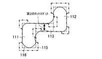
図14は端子とその接続配線の、OPC補正後の設計パターンと実際の仕上がり形状との関係を示す図である。図14では、出力端子部111と入力端子部112とが図面縦方向にずらして配置されている。そして、出力端子部111と入力端子部112とを接続するように、同一配線層に接続配線113が配置されている。すなわち、同一配線層に形成されたセル端子とその接続配線の形状が、クランク状になっている。 FIG. 14 is a diagram showing the relationship between the design pattern after OPC correction and the actual finished shape of the terminal and its connection wiring. In FIG. 14, the
図14において、115はOPC補正後の設計パターン、116は最終仕上がり形状である。図14に示すように、OPC処理によって、出力端子部111と接続配線113とに挟まれた凹部が外側に膨らむことや、入力端子112と接続配線113とに挟まれた凹部が外側に膨らむことは解消されている。ところが、接続配線113の最終仕上がり形状の端子幅が、OPC補正前の元の設計パターンと比べて小さくなっている。本願明細書では、これを第2のホットスポットという。 In FIG. 14,
従来は、設計パターン中にホットスポットとなる配線形状を検出した場合、そのような配線形状を作らないように、再度、レイアウト設計をやり直していた。つまり、半導体集積回路装置のレイアウトにホットスポットが存在すると、設計の後戻りが生じるため、半導体集積回路設計のTAT(Turn Around Time)が増大するという問題があった。 Conventionally, when a wiring shape that becomes a hot spot is detected in a design pattern, the layout design is performed again so as not to create such a wiring shape. In other words, if a hot spot exists in the layout of the semiconductor integrated circuit device, the design will be reversed, resulting in an increase in TAT (Turn Around Time) of the semiconductor integrated circuit design.
また、上述したような第1および第2のホットスポットが存在すると、配線形状の最終仕上がりの一部が細ってしまい、場合によっては配線の断線が生じるため、これが半導体集積回路装置の歩留まりを低下させる要因となってしまう。 In addition, if the first and second hot spots as described above are present, a part of the final finish of the wiring shape is thinned, and the wiring may be disconnected in some cases, which reduces the yield of the semiconductor integrated circuit device. Will be a factor.
前記の問題に鑑み、本発明は、半導体集積回路装置の設計TATの増大や歩留まり低下の要因となるホットスポットが生じにくい、標準セルの端子に係る配線構造を提供することを目的とする。 In view of the above problems, an object of the present invention is to provide a wiring structure related to the terminals of a standard cell in which a hot spot that causes an increase in design TAT and a decrease in yield of a semiconductor integrated circuit device hardly occurs.
本発明の第1態様では、第1方向において隣接して配置された第1および第2の標準セルを含む半導体集積回路装置は、前記第1の標準セルの出力端子として前記第1方向と直交する第2方向に延びるように配置された出力端子部と、前記第2の標準セルの入力端子として前記第2方向に延びるように配置された入力端子部と、前記出力端子部と前記入力端子部とを電気的に接続するように、前記第1方向に延びるように配置された接続配線とを備え、前記出力端子部、前記入力端子部および前記接続配線は、同一の金属配線層に形成されており、前記出力端子部は、前記接続配線が接続された領域を基点として、前記第2方向における第1の向きに延びている一方、前記第1の向きとは逆の第2の向きに延びておらず、前記入力端子部は、前記接続配線が接続された領域を基点として、前記第2方向における前記第2の向きに延びている一方、前記第1の向きに延びていない。 In the first aspect of the present invention, the semiconductor integrated circuit device including the first and second standard cells arranged adjacent to each other in the first direction is orthogonal to the first direction as an output terminal of the first standard cell. An output terminal portion arranged to extend in the second direction, an input terminal portion arranged to extend in the second direction as an input terminal of the second standard cell, the output terminal portion and the input terminal Connecting wires arranged to extend in the first direction so as to be electrically connected to each other, and the output terminal portion, the input terminal portion, and the connecting wires are formed in the same metal wiring layer The output terminal portion extends in a first direction in the second direction from a region to which the connection wiring is connected, and a second direction opposite to the first direction. The input terminal portion is not extended to As a base point the serial connection wiring is connected regions, while extending in the second direction in the second direction, it does not extend to the first orientation.
この第1態様によると、半導体集積回路装置において、同一方向に延びるように配置された出力端子部と入力端子部は、同一配線層に形成された、直交する方向に延びる接続配線によって接続されている。そして出力端子部は、接続配線が接続された領域を基点として、一方の向きにだけ延びている一方、入力端子部は、接続配線が接続された領域を基点として、他方の向きにだけ延びている。すなわち、出力端子部、接続配線および入力端子部は、『コ』の字状、すなわち凹形状になっておらず、上述した第1のホットスポットが生じやすい配線形状が回避されている。これにより、設計の後戻りや、あるいは、配線の断線発生による製造歩留まり低下を回避することができる。 According to the first aspect, in the semiconductor integrated circuit device, the output terminal portion and the input terminal portion arranged so as to extend in the same direction are connected by the connection wiring extending in the orthogonal direction formed in the same wiring layer. Yes. The output terminal portion extends only in one direction, starting from the region where the connection wiring is connected, while the input terminal portion extends only in the other direction, starting from the region where the connection wiring is connected. Yes. That is, the output terminal portion, the connection wiring, and the input terminal portion are not “U” -shaped, that is, not concave, and the above-described wiring shape that easily causes the first hot spot is avoided. As a result, it is possible to avoid a reduction in the manufacturing yield due to the backtracking of the design or the occurrence of disconnection of the wiring.
本発明の第2態様では、標準セルの端子構造は、前記標準セルの入力端子として第1方向に延びるように配置された入力端子部と、前記標準セルの出力端子として前記第1方向に延びるように配置された出力端子部とを備え、前記入力端子部および前記出力端子部は、前記第1方向に直交する第2方向に見て重なりを有しており、前記入力端子部は、前記重なりの領域を基点として、前記第1方向における第1の向きに延びている一方、前記第1の向きとは逆の第2の向きに延びておらず、前記出力端子部は、前記重なりの領域を基点として、前記第1方向における前記第2の向きに延びている一方、前記第1の向きに延びていない。 In the second aspect of the present invention, the terminal structure of the standard cell has an input terminal portion arranged to extend in the first direction as an input terminal of the standard cell, and extends in the first direction as an output terminal of the standard cell. The input terminal portion and the output terminal portion are overlapped when viewed in a second direction orthogonal to the first direction, and the input terminal portion is While extending in the first direction in the first direction with the overlapping region as a base point, it does not extend in the second direction opposite to the first direction, and the output terminal portion Starting from the region, it extends in the second direction in the first direction, but does not extend in the first direction.
この第2態様によると、標準セルにおいて、第1方向に延びるように配置された出力端子部と入力端子部は、これらに直交する第2方向に見て重なりを有している。そして入力端子部は、重なりの領域を基点として、一方の向きにだけ延びている一方、出力端子部は、重なりの領域を基点として、他方の向きにだけ延びている。このような端子構造を持つ標準セルを第2方向に並べて配置することによって、上述した第1のホットスポットが生じやすい配線形状を回避することができる。これにより、設計の後戻りや、あるいは、配線の断線発生による製造歩留まり低下を回避することができる。 According to the second aspect, in the standard cell, the output terminal portion and the input terminal portion arranged so as to extend in the first direction have an overlap when viewed in the second direction orthogonal thereto. The input terminal portion extends only in one direction starting from the overlapping region, while the output terminal portion extends only in the other direction starting from the overlapping region. By arranging standard cells having such a terminal structure side by side in the second direction, it is possible to avoid the above-described wiring shape in which the first hot spot is likely to occur. As a result, it is possible to avoid a reduction in the manufacturing yield due to the backtracking of the design or the occurrence of disconnection of the wiring.
本発明の第3態様では、標準セルを含む半導体集積回路装置は、前記標準セルの出力端子として、第1方向に延びるように配置された出力端子部と、前記標準セルの入力端子として、前記第1方向に延びるように配置された入力端子部と、前記出力端子部と接続されており、前記第1方向と直交する第2方向において、前記出力端子部から第1の向きに延びるように配置された第1の配線と、前記出力端子部と接続されており、前記第2方向において、前記出力端子部から前記第1の向きの逆である第2の向きに延びるように配置された第2の配線とを備え、前記出力端子部、前記入力端子部、並びに前記第1および第2の配線は、同一の金属配線層に形成されており、前記第1および第2の配線は、前記第2方向に見たとき、重なりを有しておらず、前記出力端子部の、前記第1の配線が接続された部分と前記第2の配線が接続された部分との間における端子幅は、前記入力端子部の端子幅よりも、大きい。 In a third aspect of the present invention, a semiconductor integrated circuit device including a standard cell includes an output terminal portion arranged to extend in a first direction as an output terminal of the standard cell, and an input terminal of the standard cell as the input terminal. An input terminal portion arranged to extend in a first direction and the output terminal portion are connected to each other and extend in a first direction from the output terminal portion in a second direction orthogonal to the first direction. The first wiring arranged and connected to the output terminal portion, and arranged to extend in the second direction from the output terminal portion in a second direction that is opposite to the first direction in the second direction. And the output terminal portion, the input terminal portion, and the first and second wirings are formed in the same metal wiring layer, and the first and second wirings are: Have an overlap when viewed in the second direction Orazu, the output terminal portion, the terminal width between the first wiring is connected portion and the portion where the second wiring is connected, than the terminal width of the input terminal portion is greater.
この第3態様によると、第1方向に延びる出力端子部に、第2の方向において第1の向きに延びる第1の配線と、第1の向きの逆である第2の向きに延びる第2の配線とが、接続されている。そして、第1および第2の配線は、第2の方向に見たとき、重なりを有していない。すなわち、出力端子部と第1および第2の配線が、クランク状の配線構造、すなわち、上述した第2のホットスポットが生じやすい形状の配線構造になっている。ただし、出力端子部の端子幅が、入力端子部の端子幅よりも、大きくなっているので、第2のホットスポットの発生を回避することができる。これにより、設計の後戻りや、あるいは、配線の断線発生による製造歩留まり低下を回避することができる。 According to the third aspect, the output terminal portion extending in the first direction, the first wiring extending in the first direction in the second direction, and the second direction extending in the second direction opposite to the first direction. Are connected to each other. The first and second wirings do not overlap when viewed in the second direction. That is, the output terminal portion and the first and second wirings have a crank-shaped wiring structure, that is, a wiring structure in which the above-described second hot spot is likely to occur. However, since the terminal width of the output terminal portion is larger than the terminal width of the input terminal portion, the occurrence of the second hot spot can be avoided. As a result, it is possible to avoid a reduction in the manufacturing yield due to the backtracking of the design or the occurrence of disconnection of the wiring.
本発明の第4態様では、第1方向において隣接して配置された第1および第2の標準セルを含む半導体集積回路装置は、前記第1の標準セルの出力端子として、前記第1方向と直交する第2方向に延びるように配置された出力端子部と、前記第2の標準セルの入力端子として、前記第2方向に延びるように配置された入力端子部と、前記出力端子部と前記入力端子部とを電気的に接続するように、前記第1方向に延びるように配置された接続配線とを備え、前記出力端子部、前記入力端子部および前記接続配線は、同一の金属配線層に形成されており、前記出力端子部と前記入力端子部とは、前記第2方向において、位置および長さが同一であり、前記接続配線は、配線幅が前記出力端子部および入力端子部の長さと同一であり、かつ、前記第2方向における位置が、前記出力端子部および入力端子部と同一である。 In a fourth aspect of the present invention, a semiconductor integrated circuit device including first and second standard cells arranged adjacent to each other in a first direction may be used as an output terminal of the first standard cell as the first direction. An output terminal portion disposed so as to extend in a second direction orthogonal to each other; an input terminal portion disposed so as to extend in the second direction as an input terminal of the second standard cell; the output terminal portion; A connection wiring arranged so as to extend in the first direction so as to be electrically connected to the input terminal portion, and the output terminal portion, the input terminal portion, and the connection wiring are the same metal wiring layer The output terminal portion and the input terminal portion have the same position and length in the second direction, and the connection wiring has a wiring width of the output terminal portion and the input terminal portion. Identical to the length, and said Position in two directions, is identical to the output terminal portion and the input terminal unit.
この第4態様によると、半導体集積回路装置において、同一方向に延びるように配置された出力端子部と入力端子部は、同一配線層に形成された、直交する方向に延びる接続配線によって接続されている。そして、接続配線は、配線幅が出力端子部および入力端子部の長さと同一であり、かつ、出力端子部および入力端子部が延びる方向における位置が、出力端子部および入力端子部と同一である。すなわち、出力端子、接続配線および入力端子部からなる配線構造は、『コ』の字状、すなわち凹形状にも、また、クランク状にもなっておらず、よって、上述した第1のホットスポットや第2のホットスポットが生じやすい配線形状が回避されている。これにより、設計の後戻りや、あるいは、配線の断線発生による製造歩留まり低下を回避することができる。 According to the fourth aspect, in the semiconductor integrated circuit device, the output terminal portion and the input terminal portion arranged so as to extend in the same direction are connected by the connection wiring formed in the same wiring layer and extending in the orthogonal direction. Yes. The connection wiring has the same wiring width as the length of the output terminal portion and the input terminal portion, and the position in the direction in which the output terminal portion and the input terminal portion extend is the same as the output terminal portion and the input terminal portion. . That is, the wiring structure including the output terminal, the connection wiring, and the input terminal portion is neither “U” -shaped, that is, neither concave nor crank-shaped, and thus the first hot spot described above. In addition, a wiring shape in which a second hot spot is likely to occur is avoided. As a result, it is possible to avoid a reduction in the manufacturing yield due to the backtracking of the design or the occurrence of disconnection of the wiring.
本発明によると、上述した第1および第2のホットスポットが生じにくい、標準セルの端子に係る配線構造を提供することができる。このため、設計の後戻りを回避できるのでTATの短縮を実現できるとともに、配線の断線発生を抑制できるので、製造歩留まりを向上させることができる。 According to the present invention, it is possible to provide a wiring structure relating to a terminal of a standard cell in which the first and second hot spots described above are unlikely to occur. For this reason, it is possible to avoid the backtracking of the design, so that the TAT can be shortened and the occurrence of the disconnection of the wiring can be suppressed, so that the manufacturing yield can be improved.
以下、本発明の実施の形態について、図面を参照して説明する。 Embodiments of the present invention will be described below with reference to the drawings.
(実施形態1)
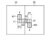
図1は実施形態1に係る半導体集積回路装置におけるセル端子とその接続配線の構造を示す模式図である。図1において、第1の標準セル10と第2の標準セル20とが、図面横方向(第1方向)において隣接して配置されている。第1の標準セル10には、図面縦方向(第2方向)に延びるように、出力端子部11が配置されている。出力端子部11は第1の標準セル10の出力端子として機能する。第2の標準セル20には、図面縦方向に延びるように、入力端子部21が配置されている。入力端子部21は第2の標準セル20の入力端子として機能する。(Embodiment 1)
FIG. 1 is a schematic diagram showing the structure of a cell terminal and its connection wiring in the semiconductor integrated circuit device according to the first embodiment. In FIG. 1, a first
接続配線25は、出力端子部11と入力端子部21とを電気的に接続するように、図面横方向に延びるように配置されている。出力端子部11、入力端子部21および接続配線25は、同一の金属配線層に形成されている。なお、出力端子部11と入力端子部21とを電気的に接続するために、これらと異なる配線層を利用して接続配線を形成することも考えられるが、この場合には、接続配線の配線長が長くなるとともに上下の配線層を接続するためのコンタクトを設ける必要がある。このため、配線長の最短化のために、例えば自動配置配線ツールでは、同一配線層における接続配線が多用される。 The
そして、出力端子部11は、接続配線25が接続された領域を基点として、図面縦方向における上向き(第1の向き)に延びている。下向き(第2の向き)には延びていない。また、入力端子部21は、接続配線25が接続された領域を基点として、図面縦方向における下向きに延びている。上向きには延びていない。すなわち、接続配線25の上側には出力端子部11のみが延びており、接続配線25の下側には入力端子部21のみが延びている。言いかえると、出力端子部11の、接続配線25が接続された領域から延びた部分(領域A11)は、図面横方向において、入力端子部21と対向していない。同様に、入力端子部21の、接続配線25が接続された領域から延びた部分(領域A21)は、図面横方向において、出力端子部11と対向していない。 The
このように本実施形態では、同一配線層に形成されたセル端子とその接続配線の形状が、『コ』の字状、すなわち凹形状になっていない。すなわち、上述した第1のホットスポットが生じやすい配線形状が未然に回避されている。これにより、設計の後戻り、あるいは配線の断線発生による製造歩留まり低下を回避することができる。また、凹形状の配線構造の場合、例えば出力端子部のマスクを拡げようとすると、対向する配線部分すなわち入力端子部との干渉が生じやすいため、困難である。これに対して本実施形態では、出力端子部11および入力端子部21のいずれも、対向する配線部分が存在しないため、マスクを容易に拡げることができる。 As described above, in this embodiment, the shape of the cell terminal formed in the same wiring layer and the connection wiring thereof is not a “U” shape, that is, a concave shape. That is, the above-described wiring shape in which the first hot spot is likely to occur is avoided in advance. As a result, it is possible to avoid a reduction in manufacturing yield due to the backtracking of the design or the occurrence of wire breakage. In the case of a concave wiring structure, for example, if the mask of the output terminal portion is to be expanded, it is difficult to cause interference with the opposing wiring portion, that is, the input terminal portion, which is difficult. On the other hand, in this embodiment, since neither the
また、図1の構成では、クランク状の配線構造、すなわち、上述した第2のホットスポットが生じやすい形状の配線構造になっている。このため、第2のホットスポットの発生を回避するためには、接続配線25の配線幅W25は、図1中破線で示したように、出力端子部11の端子幅W11および入力端子部21の端子幅W21以上であることが好ましい。 Further, the configuration of FIG. 1 has a crank-shaped wiring structure, that is, a wiring structure in which the above-described second hot spot is likely to occur. Therefore, in order to avoid the occurrence of the second hot spot, the wiring width W25 of the
なお、図1の構成では、出力端子部11の下辺は接続配線25の下辺とほぼ同一直線上に位置しているが、これに限られるものではなく、例えば、出力端子部11の下辺が接続配線25の上辺と下辺との間に位置しており、接続配線25の左辺が出力端子部11の左辺の位置まで延びていてもよい。同様に、入力端子部21の上辺は接続配線25の上辺とほぼ同一直線上に位置しているが、これに限られるものではなく、例えば、入力端子部21の上辺が接続配線31の上辺と下辺との間に位置しており、接続配線25の右辺が入力端子部21の右辺の位置まで延びていてもよい。 In the configuration of FIG. 1, the lower side of the
また、出力端子部11は、第1の標準セル10の、第2の標準セル20に最も近い出力端子を構成するものであることが好ましい。また、入力端子部21は、第2の標準セル20の、第1の標準セル10に最も近い出力端子を構成するものであることが好ましい。 Moreover, it is preferable that the
(実施形態2)
図2は実施形態2に係る半導体集積回路装置におけるセル端子とその接続配線の構造を示す模式図である。図2において、図1と共通の構成要素には図1と同一の符号を付しており、ここではその詳細な説明を省略する。(Embodiment 2)
FIG. 2 is a schematic diagram showing the structure of the cell terminal and its connection wiring in the semiconductor integrated circuit device according to the second embodiment. 2, the same reference numerals as those in FIG. 1 are attached to the same components as those in FIG. 1, and detailed description thereof is omitted here.
図2の構成でも図1と同様に、出力端子部11Aの、接続配線25が接続された領域から上向きに延びた部分は、図面横方向において、入力端子部21Aと対向しておらず、入力端子部21Aの、接続配線25が接続された領域から下向きに延びた部分は、図面横方向において、出力端子部11Aと対向していない。すなわち、同一配線層に形成されたセル端子とその接続配線の形状が、『コ』の字状、すなわち凹形状になっておらず、上述した第1のホットスポットが生じやすい配線形状が未然に回避されている。 2, the portion of the
さらに本実施形態では、出力端子部11Aは、図面横方向における接続配線25とは逆の方(左方)に突出するように形成された突出部13を有している。また、入力端子部21Aは、図面横方向における接続配線25とは逆の方(右方)に突出するように形成された突出部23を有している。 Further, in the present embodiment, the
例えば自動配置配線ツールでは、一般的に、標準セルの入力端子または出力端子の形状面積が大きいほど、端子間の配線接続が容易になり、配線混雑が緩和される傾向がある。このため、本実施形態のように、出力端子部11Aに突出部13を設けるとともに入力端子部21Aに突出部23を設けることによって、端子部の面積が大きくなるので、端子間の配線混雑が緩和されるという効果を得ることができる。しかも、突出部13,23は図面横方向に突出するように設けられているので、実施形態1の配線構造におけるホットスポットが生じにくいという効果を損なうことがない。 For example, in an automatic placement and routing tool, generally, as the shape area of an input terminal or output terminal of a standard cell is larger, wiring connection between terminals becomes easier and wiring congestion tends to be reduced. For this reason, as in the present embodiment, by providing the
なお、本実施形態では、出力端子部と入力端子部の両方が突出部を有するものとしたが、これに限られるものではなく、出力端子部と入力端子部のいずれか一方のみが、接続配線とは逆の方に突出するように形成された突出部を有していてもかまわない。この場合も、本実施形態と同様の効果が得られる。 In this embodiment, both the output terminal portion and the input terminal portion have protrusions. However, the present invention is not limited to this, and only one of the output terminal portion and the input terminal portion is connected to the connection wiring. You may have the protrusion part formed so that it might protrude in the opposite direction. In this case, the same effect as that of the present embodiment can be obtained.
(実施形態3)
図3(A)は実施形態3に係る標準セルの端子構造を示す模式図である。図3(A)において、標準セル30には、図面縦方向(第1方向)に延びるように、入力端子部31と出力端子部32とが配置されている。入力端子部31は標準セル30の入力端子として機能し、出力端子部32は標準セル30の出力端子として機能する。(Embodiment 3)
FIG. 3A is a schematic diagram illustrating a terminal structure of a standard cell according to the third embodiment. In FIG. 3A, an
入力端子部31および出力端子部32は、図面横方向(第2方向)に見て、重なりを有している(領域OV1)。そして、入力端子部31は、この重なり領域OV1を基点として、図面縦方向における下向き(第1の向き)に延びている。上向き(第2の向き)には延びていない。また、出力端子部32は、この重なり領域OV1を基点として、図面縦方向における上向き(第2の向き)に延びている。下向き(第1の向き)には延びていない。すなわち、重なり領域OV1の下側には入力端子部31のみが延びており、重なり領域OV1の上側には出力端子部32のみが延びている。言いかえると、入力端子部31の、重なり領域OV1から延びた部分(領域A31)は、図面横方向において、出力端子部32と対向していない。同様に、出力端子部32の、重なり領域OV1から延びた部分(領域A32)は、図面横方向において、入力端子部31と対向していない。入力端子部31と出力端子部32とが対向しているのは、重なり領域OV1の範囲のみである。 The
図3(B)は図3(A)の標準セルを用いた半導体集積回路装置におけるセル端子とその接続配線の構造を示す模式図である。図3(B)において、第1の標準セル30aと第2の標準セル30bとが図面横方向において隣接して配置されている。第1の標準セル30aおよび第2の標準セル30bはともに、図3(A)の標準セル30と同様の端子構造を有している。すなわち、第1の標準セル30aは、図3(A)と同様の、入力端子部41および出力端子部42を有しており、第2の標準セル30bは、図3(A)と同様の、入力端子部43および出力端子部44を有している。なお、第1の標準セル30aと第2の標準セル30bの機能は、同一の場合もあるし、異なっている場合もある。 FIG. 3B is a schematic diagram showing the structure of the cell terminal and its connection wiring in the semiconductor integrated circuit device using the standard cell of FIG. In FIG. 3B, a first
そして、例えば自動配置配線ツールによって、接続配線45が配置される。接続配線45は、第1の標準セル30aの出力端子部42と第2の標準セル30bの入力端子部43とを電気的に接続するように、図面横方向に延びるように配置されている。また接続配線45は、出力端子部42および入力端子部43と同一の金属配線層に形成されている。 Then, for example, the
図3(B)に示すように、同一配線層に形成されたセル端子とその接続配線の形状が、『コ』の字状、すなわち凹形状になっていない。すなわち、図3(A)に示すような端子構造を有する標準セルを用いることによって、上述した第1のホットスポットが生じやすい配線形状を未然に回避することができる。これにより、設計の後戻り、あるいは配線の断線発生による製造歩留まり低下を回避することができる。 As shown in FIG. 3B, the shape of the cell terminal formed in the same wiring layer and its connection wiring is not “U”, that is, a concave shape. That is, by using a standard cell having a terminal structure as shown in FIG. 3A, it is possible to avoid the above-described wiring shape in which the first hot spot is likely to occur. As a result, it is possible to avoid a reduction in manufacturing yield due to the backtracking of the design or the occurrence of wire breakage.
なお、標準セルの構成によっては、入力端子および出力端子の一方または両方が、複数設けられている場合がある。この場合、標準セルの中で最も外側にある入力端子と、その逆側の最も外側にある出力端子とが、図3(A)に示すような関係にあれば、本実施形態の効果が得られる。すなわち、入力端子部31は、図面横方向における両側の外郭のうちの一方(図では左側の外郭)に最も近い入力端子を構成するものであり、出力端子部32は、図面横方向における両側の外郭のうちの他方(図では右側の外郭)に最も近い出力端子を構成するものであるのが好ましい。 Depending on the configuration of the standard cell, a plurality of one or both of input terminals and output terminals may be provided. In this case, if the outermost input terminal in the standard cell and the outermost output terminal on the opposite side have a relationship as shown in FIG. It is done. That is, the
(実施形態4)
図4は実施形態4に係る標準セルの端子構造を示す模式図である。図4において、図3(A)と共通の構成要素には図3(A)と同一の符号を付しており、ここではその詳細な説明を省略する。(Embodiment 4)
FIG. 4 is a schematic diagram illustrating a terminal structure of a standard cell according to the fourth embodiment. In FIG. 4, the same components as those in FIG. 3A are denoted by the same reference numerals as those in FIG. 3A, and detailed description thereof is omitted here.
図4の構成でも図3(A)と同様に、入力端子部31Aおよび出力端子部32Aは、図面横方向に見て、重なりを有している。そして、入力端子部31Aの、重なり領域から下向きに延びた部分は、図面横方向において、出力端子部32Aと対向しておらず、出力端子部32Aの、重なり領域から上向きに延びた部分は、図面横方向において、入力端子部31Aと対向していない。すなわち、図4に示すような端子構造を有する標準セルを用いることによって、上述した第1のホットスポットが生じやすい『コ』の字状、すなわち凹形状の配線形状を未然に回避することができる。 In the configuration of FIG. 4, as in FIG. 3A, the
さらに本実施形態では、入力端子部31Aは、図面横方向における、標準セル30の中心CENの方(左方)に突出するように形成された突出部33を有している。また、出力端子部32Aは、図面横方向における、標準セル30の中心CENの方(右方)に突出するように形成された突出部34を有している。 Furthermore, in the present embodiment, the
例えば自動配置配線ツールでは、一般的に、標準セルの入力端子または出力端子の形状面積が大きいほど、端子間の配線接続が容易になり、配線混雑が緩和される傾向がある。このため、本実施形態のように、入力端子部31Aに突出部33を設けるとともに出力端子部32Aに突出部34を設けることによって、端子部の面積が大きくなるので、端子間の配線混雑が緩和されるという効果を得ることができる。しかも、突出部33,34は図面横方向に突出するように設けられているので、実施形態3のセル端子構造におけるホットスポットが生じにくいという効果を損なうことがない。 For example, in an automatic placement and routing tool, generally, as the shape area of an input terminal or output terminal of a standard cell is larger, wiring connection between terminals becomes easier and wiring congestion tends to be reduced. For this reason, since the area of a terminal part becomes large by providing the
なお、本実施形態では、出力端子部と入力端子部の両方が突出部を有するものとしたが、これに限られるものではなく、出力端子部と入力端子部のいずれか一方のみが、標準セルの中心の方に突出するように形成された突出部を有していてもかまわない。この場合も、本実施形態と同様の効果が得られる。 In the present embodiment, both the output terminal portion and the input terminal portion have protrusions. However, the present invention is not limited to this, and only one of the output terminal portion and the input terminal portion is a standard cell. You may have the protrusion part formed so that it might protrude toward the center of. In this case, the same effect as that of the present embodiment can be obtained.
(実施形態5)
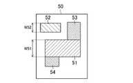
図5は実施形態5に係る半導体集積回路装置におけるセル端子とその接続配線の構造を示す模式図である。図5において、標準セル50には、図面横方向(第1方向)に延びるように、出力端子部51と入力端子部52とが配置されている。出力端子部51は標準セル50の出力端子として機能し、入力端子部52は標準セル50の入力端子として機能する。(Embodiment 5)
FIG. 5 is a schematic diagram showing the structure of the cell terminals and their connection wirings in the semiconductor integrated circuit device according to the fifth embodiment. In FIG. 5, an
そして、出力端子部51には、第1の配線53と第2の配線54とが接続されている。このような配線53,54は、例えば、出力端子部51のファンアウト数が2以上の場合に、自動配置配線ツールによって配置される。第1の配線53は、図面縦方向(第2方向)において、出力端子部51から上向き(第1の向き)に延びるように配置されている。一方、第2の配線54は、図面縦方向において、出力端子部51から下向き(第2の向き)に延びるように配置されている。出力端子部51、入力端子部52、並びに第1および第2の配線53,54は、同一の金属配線層に形成されている。 The
ここで、第1および第2の配線53,54は、図面縦方向に見たとき、重なりを有していない。すなわち、出力端子部51並びに第1および第2の配線53,54は、クランク状の配線構造、すなわち、上述した第2のホットスポットが生じやすい形状の配線構造になっている。そこで、第2のホットスポットの発生を回避するために、出力端子部51の配線幅W51を大きく設定している。ここでは、出力端子部51の、第1の配線53が接続された部分と第2の配線54が接続された部分との間における端子幅W51は、入力端子部52の端子幅W52よりも、大きくなっている。これにより、第2のホットスポットの発生を回避できるので、設計の後戻り、あるいは配線の断線発生による製造歩留まり低下を回避することができる。 Here, the first and
図6は標準セル50の、出力端子部53に関連する内部構造の一例を示す図である。図6に示すように、標準セル50の外郭に隣接して、ゲート電極55を共有したトランジスタ56,57が配置されている。出力端子部53は、トランジスタ56,57のドレインと接続されたセル内配線58と、コンタクト59を介して接続されている。 FIG. 6 is a diagram showing an example of an internal structure related to the
図7は本実施形態に係る半導体集積回路装置におけるセル端子とその接続配線の構造の他の例を示す模式図である。図7において、図5と共通の構成要素には図5と同一の符号を付しており、ここではその詳細な説明を省略する。図7の構成では、出力端子部51と入力端子部52とが、図面縦方向に見たとき、重なりを有している。それ以外は図5と同様である。すなわち、出力端子部51並びに第1および第2の配線53,54は、クランク状の配線構造、すなわち、上述した第2のホットスポットが生じやすい形状の配線構造になっている。そして、出力端子部51の、第1の配線53が接続された部分と第2の配線54が接続された部分との間における端子幅W51は、入力端子部52の端子幅W52よりも、大きくなっている。これにより、図5と同様に、第2のホットスポットの発生を回避できるので、設計の後戻り、あるいは配線の断線発生による製造歩留まり低下を回避することができる。 FIG. 7 is a schematic view showing another example of the structure of the cell terminal and its connection wiring in the semiconductor integrated circuit device according to this embodiment. In FIG. 7, the same components as those in FIG. 5 are denoted by the same reference numerals as those in FIG. 5, and detailed description thereof is omitted here. In the configuration of FIG. 7, the
(実施形態6)
図8は実施形態6に係る半導体集積回路装置におけるセル端子とその接続配線の構造を示す模式図である。図8において、第1の標準セル60と第2の標準セル70とが、図面横方向(第1方向)において隣接して配置されている。第1の標準セル60には、図面縦方向(第2方向)に延びるように、出力端子部61が配置されている。出力端子部61は第1の標準セル60の出力端子として機能する。第2の標準セル20には、図面縦方向に延びるように、入力端子部71が配置されている。入力端子部71は第2の標準セル70の入力端子として機能する。(Embodiment 6)
FIG. 8 is a schematic diagram showing the structure of cell terminals and their connection wirings in the semiconductor integrated circuit device according to the sixth embodiment. In FIG. 8, a first
接続配線65は、出力端子部61と入力端子部71とを電気的に接続するように、図面横方向に延びるように配置されている。出力端子部61、入力端子部71および接続配線65は、同一の金属配線層に形成されている。接続配線65は、例えば自動配置配線ツールによって配置される。 The
ここで、出力端子部61と入力端子部71とは、図面縦方向において、位置および長さが同一である。そして、接続配線65は、配線幅W65が、出力端子部61の長さL61および入力端子部71の長さL71と同一であり、かつ、図面縦方向における位置が、出力端子部61および入力端子部71と同一である。言いかえると、図面横方向に見たとき、出力端子部61、入力端子部71および接続配線65は、ほぼぴったりと重なっている。 Here, the
このように本実施形態では、同一配線層に形成されたセル端子とその接続配線の形状が、『コ』の字状すなわち凹形状になっておらず、また、クランク状にもなっていない。すなわち、上述した第1のホットスポットや第2のホットスポットが生じやすい配線形状になっていない。このため、ホットスポットの発生を回避できるので、設計の後戻り、あるいは配線の断線発生による製造歩留の低下を回避することができる。 As described above, in this embodiment, the shape of the cell terminal formed in the same wiring layer and the connection wiring thereof is not a “U” shape, that is, a concave shape, and is not a crank shape. That is, the wiring shape is not likely to cause the first hot spot or the second hot spot described above. For this reason, the occurrence of hot spots can be avoided, so that it is possible to avoid a decrease in manufacturing yield due to a backward design or occurrence of disconnection of wiring.
さらに本実施形態では、出力端子部61は、図面横方向における接続配線65とは逆の方(左方)に突出するように形成された突出部63を有している。また、入力端子部71は、図面横方向における接続配線65とは逆の方(右方)に突出するように形成された突出部73を有している。これにより、端子部の面積が大きくなるので、端子間の配線混雑が緩和されるという効果を得ることができる。しかも、突出部63,73は図面横方向に突出するように設けられているので、ホットスポットが生じにくいという効果を損なうことがない。 Furthermore, in this embodiment, the
なお、本実施形態では、出力端子部と入力端子部の両方が突出部を有するものとしたが、これに限られるものではなく、出力端子部と入力端子部のいずれか一方のみが、接続配線とは逆の方に突出するように形成された突出部を有していてもかまわない。この場合も、本実施形態と同様の効果が得られる。 In this embodiment, both the output terminal portion and the input terminal portion have protrusions. However, the present invention is not limited to this, and only one of the output terminal portion and the input terminal portion is connected to the connection wiring. You may have the protrusion part formed so that it might protrude in the opposite direction. In this case, the same effect as that of the present embodiment can be obtained.
図9は上述の実施形態に係る配線構造を標準セルに採用した場合の、実際の半導体集積回路装置のレイアウト構造の一例を示す図である。図9では、矩形枠で示される標準セルが縦横に並べて配置されており、所定の論理を構成している。そして、上述の実施形態を採用した標準セルを太枠で囲んで示している。すなわち、最上列左側の2個の標準セル10,20に、図1に示した配線構造が採用されており、最下列左端の標準セル50に、図7に示した配線構造が採用されている。図9において、図1および図7と共通の構成要素には図1および図7と同一の符号を付している。 FIG. 9 is a diagram showing an example of a layout structure of an actual semiconductor integrated circuit device when the wiring structure according to the above-described embodiment is adopted for a standard cell. In FIG. 9, standard cells indicated by rectangular frames are arranged side by side in the vertical and horizontal directions, and constitute a predetermined logic. And the standard cell which employ | adopted the above-mentioned embodiment is enclosed and shown with the thick frame. That is, the wiring structure shown in FIG. 1 is adopted for the two
図10は図9の標準セル10,20の構造を詳細に示す図であり、(a)は論理図、(b)は平面図、(c)は(b)におけるB−B断面図、(d)は(b)におけるA−A断面図である。また、図11は図9の標準セル50の構造を示す図であり、(a)は論理図、(b)は平面図、(c)は(b)におけるC−C断面図、(d)は(b)におけるD−D断面図である。 10 is a diagram showing in detail the structure of the
図12は上述の実施形態に係る配線構造を標準セルに採用した場合の、実際の半導体集積回路装置のレイアウト構造の他の例を示す図である。図12でも図9と同様に、矩形枠で示される標準セルが縦横に並べて配置されており、所定の論理を構成している。そして、上述の実施形態を採用した標準セルを太枠で囲んで示している。すなわち、最上列左側の2個の標準セル10,20に、図1に示した配線構造が採用されており、中央列中央の標準セル50に、図7に示した配線構造が採用されている。図12において、図1および図7と共通の構成要素には図1および図7と同一の符号を付している。 FIG. 12 is a diagram showing another example of a layout structure of an actual semiconductor integrated circuit device when the wiring structure according to the above-described embodiment is adopted as a standard cell. In FIG. 12, as in FIG. 9, standard cells indicated by a rectangular frame are arranged vertically and horizontally to constitute a predetermined logic. And the standard cell which employ | adopted the above-mentioned embodiment is enclosed and shown with the thick frame. That is, the wiring structure shown in FIG. 1 is adopted for the two
なお、図9および図12では、図1および図7に示した配線構造を標準セルに採用した例を示したが、上述の各実施形態で説明したその他の配線構造についても、同様に、標準セルに採用して、実際の半導体集積回路装置のレイアウト構造に適用することは可能である。 9 and 12 show examples in which the wiring structure shown in FIG. 1 and FIG. 7 is adopted as a standard cell, the other wiring structures described in the above embodiments are also standardized. It can be applied to a layout structure of an actual semiconductor integrated circuit device by adopting it in a cell.
本発明では、ホットスポットが生じにくい、標準セルの端子に係る配線構造を提供することができるので、半導体集積回路装置のTATの短縮や製造歩留まりの向上を実現することができる。このため、例えば、LSIの製造期間短縮やコストダウンに有効である。 According to the present invention, it is possible to provide a wiring structure related to a standard cell terminal that is unlikely to generate a hot spot. Therefore, it is possible to reduce the TAT of the semiconductor integrated circuit device and improve the manufacturing yield. For this reason, for example, it is effective for shortening the manufacturing period of LSI and reducing the cost.
10 第1の標準セル
11,11A 出力端子部
12 第1の標準セルの外郭
13 突出部
20 第2の標準セル
21,21A 入力端子部
22 第2の標準セルの外郭
23 突出部
25 接続配線
30,30a,30b 標準セル
31,31A,41,43 入力端子部
32,32A,42,44 出力端子部
33,34 突出部
35 標準セルの外郭
50 標準セル
51 出力端子部
52 入力端子部
53 第1の配線
54 第2の配線
60 第1の標準セル
61 出力端子部
63 突出部
65 接続配線
70 第2の標準セル
71 入力端子部
73 突出部
CEN 標準セルの中心DESCRIPTION OF
Claims (10)
Translated fromJapanese前記第1の標準セルの出力端子として、前記第1方向と直交する第2方向に延びるように配置された出力端子部と、
前記第2の標準セルの入力端子として、前記第2方向に延びるように配置された入力端子部と、
前記出力端子部と前記入力端子部とを電気的に接続するように、前記第1方向に延びるように配置された接続配線とを備え、
前記出力端子部、前記入力端子部および前記接続配線は、同一の金属配線層に形成されており、
前記出力端子部は、前記接続配線が接続された領域を基点として、前記第2方向における第1の向きに延びている一方、前記第1の向きとは逆の第2の向きに延びておらず、
前記入力端子部は、前記接続配線が接続された領域を基点として、前記第2方向における前記第2の向きに延びている一方、前記第1の向きに延びていない
ことを特徴とする半導体集積回路装置。A semiconductor integrated circuit device including first and second standard cells arranged adjacent to each other in a first direction,
As an output terminal of the first standard cell, an output terminal portion arranged to extend in a second direction orthogonal to the first direction;
As an input terminal of the second standard cell, an input terminal portion arranged to extend in the second direction;
A connection wiring arranged to extend in the first direction so as to electrically connect the output terminal portion and the input terminal portion;
The output terminal portion, the input terminal portion and the connection wiring are formed in the same metal wiring layer,
The output terminal portion extends in a first direction in the second direction starting from a region where the connection wiring is connected, but does not extend in a second direction opposite to the first direction. Without
The semiconductor integrated circuit characterized in that the input terminal portion extends in the second direction in the second direction from the region where the connection wiring is connected, but does not extend in the first direction. Circuit device.
前記出力端子部および前記入力端子部のうち少なくともいずれか一方は、前記第1方向における前記接続配線とは逆の方に突出するように形成された、突出部を有している
ことを特徴とする半導体集積回路装置。The semiconductor integrated circuit device according to claim 1.
At least one of the output terminal portion and the input terminal portion has a protruding portion formed so as to protrude in the opposite direction to the connection wiring in the first direction. A semiconductor integrated circuit device.
前記出力端子部は、前記第1の標準セルの、前記第2の標準セルに最も近い出力端子を構成するものであり、
前記入力端子部は、前記第2の標準セルの、前記第1の標準セルに最も近い入力端子を構成するものである
ことを特徴とする半導体集積回路装置。The semiconductor integrated circuit device according to claim 1 or 2,
The output terminal portion constitutes an output terminal of the first standard cell closest to the second standard cell,
The semiconductor integrated circuit device, wherein the input terminal portion constitutes an input terminal of the second standard cell that is closest to the first standard cell.
前記接続配線の配線幅は、前記出力端子部および入力端子部の端子幅以上である
ことを特徴とする半導体集積回路装置。The semiconductor integrated circuit device according to any one of claims 1 to 3,
The semiconductor integrated circuit device according to claim 1, wherein a wiring width of the connection wiring is equal to or greater than a terminal width of the output terminal portion and the input terminal portion.
前記標準セルの入力端子として、第1方向に延びるように配置された入力端子部と、
前記標準セルの出力端子として、前記第1方向に延びるように配置された出力端子部とを備え、
前記入力端子部および前記出力端子部は、前記第1方向に直交する第2方向に見て、重なりを有しており、
前記入力端子部は、前記重なりの領域を基点として、前記第1方向における第1の向きに延びている一方、前記第1の向きとは逆の第2の向きに延びておらず、
前記出力端子部は、前記重なりの領域を基点として、前記第1方向における前記第2の向きに延びている一方、前記第1の向きに延びていない
ことを特徴とする標準セルの端子構造。A standard cell terminal structure,
As an input terminal of the standard cell, an input terminal portion arranged to extend in the first direction;
An output terminal portion arranged to extend in the first direction as an output terminal of the standard cell;
The input terminal portion and the output terminal portion have an overlap when viewed in a second direction orthogonal to the first direction,
The input terminal portion extends in the first direction in the first direction from the overlapping region as a base point, but does not extend in the second direction opposite to the first direction,
The terminal structure of a standard cell, wherein the output terminal portion extends in the second direction in the first direction with the overlapping region as a base point, but does not extend in the first direction.
前記入力端子部および前記出力端子部のうち少なくともいずれか一方は、前記第2方向における、前記標準セルの中心の方に突出するように形成された、突出部を有している
ことを特徴とする標準セルの端子構造。The terminal structure of the standard cell according to claim 5,
At least one of the input terminal portion and the output terminal portion has a protruding portion formed so as to protrude toward the center of the standard cell in the second direction. Standard cell terminal structure.
前記入力端子部は、前記標準セルの、前記第2方向における両側の外郭のうちの一方に最も近い入力端子を構成するものであり、
前記出力端子部は、前記標準セルの、前記第2方向における両側の外郭のうちの他方に最も近い出力端子を構成するものである
ことを特徴とする標準セルの端子構造。In the standard cell terminal structure according to claim 5 or 6,
The input terminal portion constitutes an input terminal closest to one of the outlines on both sides in the second direction of the standard cell,
The terminal structure of a standard cell, wherein the output terminal portion constitutes an output terminal that is closest to the other of the outlines on both sides in the second direction of the standard cell.
前記標準セルの出力端子として、第1方向に延びるように配置された出力端子部と、
前記標準セルの入力端子として、前記第1方向に延びるように配置された入力端子部と、
前記出力端子部と接続されており、前記第1方向と直交する第2方向において、前記出力端子部から第1の向きに延びるように配置された第1の配線と、
前記出力端子部と接続されており、前記第2方向において、前記出力端子部から前記第1の向きの逆である第2の向きに延びるように配置された第2の配線とを備え、
前記出力端子部、前記入力端子部、並びに前記第1および第2の配線は、同一の金属配線層に形成されており、
前記第1および第2の配線は、前記第2方向に見たとき、重なりを有しておらず、
前記出力端子部の、前記第1の配線が接続された部分と前記第2の配線が接続された部分との間における端子幅は、前記入力端子部の端子幅よりも、大きい
ことを特徴とする半導体集積回路装置。A semiconductor integrated circuit device including a standard cell,
As an output terminal of the standard cell, an output terminal portion arranged to extend in the first direction;
As an input terminal of the standard cell, an input terminal portion arranged to extend in the first direction;
A first wiring connected to the output terminal portion and arranged to extend in a first direction from the output terminal portion in a second direction orthogonal to the first direction;
A second wiring connected to the output terminal portion and disposed in the second direction so as to extend from the output terminal portion in a second direction that is opposite to the first direction;
The output terminal portion, the input terminal portion, and the first and second wirings are formed in the same metal wiring layer,
The first and second wirings do not overlap when viewed in the second direction,
The terminal width of the output terminal portion between the portion connected to the first wiring and the portion connected to the second wiring is larger than the terminal width of the input terminal portion. A semiconductor integrated circuit device.
前記第1の標準セルの出力端子として、前記第1方向と直交する第2方向に延びるように配置された出力端子部と、
前記第2の標準セルの入力端子として、前記第2方向に延びるように配置された入力端子部と、
前記出力端子部と前記入力端子部とを電気的に接続するように、前記第1方向に延びるように配置された接続配線とを備え、
前記出力端子部、前記入力端子部および前記接続配線は、同一の金属配線層に形成されており、
前記出力端子部と前記入力端子部とは、前記第2方向において、位置および長さが同一であり、
前記接続配線は、配線幅が前記出力端子部および入力端子部の長さと同一であり、かつ、前記第2方向における位置が、前記出力端子部および入力端子部と同一である
ことを特徴とする半導体集積回路装置。A semiconductor integrated circuit device including first and second standard cells arranged adjacent to each other in a first direction,
As an output terminal of the first standard cell, an output terminal portion arranged to extend in a second direction orthogonal to the first direction;
As an input terminal of the second standard cell, an input terminal portion arranged to extend in the second direction;
A connection wiring arranged to extend in the first direction so as to electrically connect the output terminal portion and the input terminal portion;
The output terminal portion, the input terminal portion and the connection wiring are formed in the same metal wiring layer,
The output terminal portion and the input terminal portion have the same position and length in the second direction,
The connection wiring has a wiring width that is the same as the length of the output terminal portion and the input terminal portion, and a position in the second direction is the same as the output terminal portion and the input terminal portion. Semiconductor integrated circuit device.
前記出力端子部および前記入力端子部のうち少なくともいずれか一方は、前記第1方向における前記接続配線とは逆の方に突出するように形成された、突出部を有している
ことを特徴とする半導体集積回路装置。The semiconductor integrated circuit device according to claim 9.
At least one of the output terminal portion and the input terminal portion has a protruding portion formed so as to protrude in the opposite direction to the connection wiring in the first direction. A semiconductor integrated circuit device.
Priority Applications (3)
| Application Number | Priority Date | Filing Date | Title |
|---|---|---|---|
| JP2010113537AJP2011242541A (en) | 2010-05-17 | 2010-05-17 | Semiconductor integrated circuit device, and terminal structure of standard cell |
| PCT/JP2011/000981WO2011145242A1 (en) | 2010-05-17 | 2011-02-22 | Semiconductor integrated circuit device and terminal construction of reference cell |
| US13/621,055US20130009275A1 (en) | 2010-05-17 | 2012-09-15 | Semiconductor integrated circuit device and terminal structure of standard cell |
Applications Claiming Priority (1)
| Application Number | Priority Date | Filing Date | Title |
|---|---|---|---|
| JP2010113537AJP2011242541A (en) | 2010-05-17 | 2010-05-17 | Semiconductor integrated circuit device, and terminal structure of standard cell |
Publications (1)
| Publication Number | Publication Date |
|---|---|
| JP2011242541Atrue JP2011242541A (en) | 2011-12-01 |
Family
ID=44991365
Family Applications (1)
| Application Number | Title | Priority Date | Filing Date |
|---|---|---|---|
| JP2010113537AWithdrawnJP2011242541A (en) | 2010-05-17 | 2010-05-17 | Semiconductor integrated circuit device, and terminal structure of standard cell |
Country Status (3)
| Country | Link |
|---|---|
| US (1) | US20130009275A1 (en) |
| JP (1) | JP2011242541A (en) |
| WO (1) | WO2011145242A1 (en) |
Families Citing this family (2)
| Publication number | Priority date | Publication date | Assignee | Title |
|---|---|---|---|---|
| US10579771B2 (en)* | 2017-06-14 | 2020-03-03 | Samsung Electronics Co., Ltd. | Integrated circuit including standard cells overlapping each other and method of generating layout of the integrated circuit |
| US10141297B1 (en)* | 2017-12-04 | 2018-11-27 | Qualcomm Incorporated | Integrated device comprising device level cells with variable sizes for heat dissipation around hotspots |
Family Cites Families (42)
| Publication number | Priority date | Publication date | Assignee | Title |
|---|---|---|---|---|
| IT1191188B (en)* | 1982-04-15 | 1988-02-24 | Cselt Centro Studi Lab Telecom | ELEMENTARY CELL FOR INTEGRATED CIRCUIT LOGIC DOOR NETWORKS |
| JPH0682801B2 (en)* | 1983-12-23 | 1994-10-19 | 株式会社日立製作所 | Semiconductor memory device and layout method thereof |
| JPS6114734A (en)* | 1984-06-29 | 1986-01-22 | Fujitsu Ltd | Manufacture of semiconductor integrated circuit device |
| JPH06105757B2 (en)* | 1987-02-13 | 1994-12-21 | 富士通株式会社 | Master slice type semiconductor integrated circuit |
| JP3720064B2 (en)* | 1994-01-20 | 2005-11-24 | 株式会社ルネサステクノロジ | Semiconductor integrated circuit |
| US5763944A (en)* | 1994-08-01 | 1998-06-09 | Nec Corporation | Semiconductor device having a reduced wiring area in and out of data path zone |
| US6335130B1 (en)* | 2000-05-01 | 2002-01-01 | Asml Masktools Netherlands B.V. | System and method of providing optical proximity correction for features using phase-shifted halftone transparent/semi-transparent features |
| JP3390408B2 (en)* | 2000-05-29 | 2003-03-24 | エヌイーシーマイクロシステム株式会社 | Semiconductor integrated circuit |
| US6667865B2 (en)* | 2000-09-11 | 2003-12-23 | Texas Instruments Incorporated | Efficient design of substrate triggered ESD protection circuits |
| US7155698B1 (en)* | 2001-09-11 | 2006-12-26 | The Regents Of The University Of California | Method of locating areas in an image such as a photo mask layout that are sensitive to residual processing effects |
| JP2003255508A (en)* | 2002-02-28 | 2003-09-10 | Oki Electric Ind Co Ltd | Correction method for mask pattern, photomask, exposure method and semiconductor device |
| US6892370B2 (en)* | 2003-04-02 | 2005-05-10 | Silicon Design Systems Ltd. | Computerized standard cell library for designing integrated circuits (ICs) with high metal layer intra cell signal wiring, and ICs including same |
| JP2005175001A (en)* | 2003-12-08 | 2005-06-30 | Seiko Epson Corp | Semiconductor integrated circuit |
| US7084476B2 (en)* | 2004-02-26 | 2006-08-01 | International Business Machines Corp. | Integrated circuit logic with self compensating block delays |
| JP4593236B2 (en)* | 2004-10-29 | 2010-12-08 | 株式会社日立ハイテクノロジーズ | Dimensional measurement scanning electron microscope system, circuit pattern shape evaluation system and method |
| JP4768251B2 (en)* | 2004-11-01 | 2011-09-07 | 株式会社東芝 | Semiconductor integrated circuit design method, semiconductor integrated circuit design system, and semiconductor integrated circuit manufacturing method |
| JP4817746B2 (en)* | 2005-07-27 | 2011-11-16 | 株式会社東芝 | Semiconductor device design data processing method, program thereof, and semiconductor device manufacturing method |
| JP2007042797A (en)* | 2005-08-02 | 2007-02-15 | Matsushita Electric Ind Co Ltd | Semiconductor integrated circuit |
| JP4796817B2 (en)* | 2005-10-31 | 2011-10-19 | エルピーダメモリ株式会社 | Basic cell design method, layout design method, design apparatus, and program |
| US7956421B2 (en)* | 2008-03-13 | 2011-06-07 | Tela Innovations, Inc. | Cross-coupled transistor layouts in restricted gate level layout architecture |
| US7723806B2 (en)* | 2006-03-28 | 2010-05-25 | Taiwan Semiconductor Manufacturing Co., Ltd. | Memory cells and semiconductor memory device using the same |
| JP2007317814A (en)* | 2006-05-25 | 2007-12-06 | Matsushita Electric Ind Co Ltd | Semiconductor integrated circuit using standard cell and its design method |
| US7873929B2 (en)* | 2006-08-14 | 2011-01-18 | The Regents Of The University Of California | Method, apparatus and system for designing an integrated circuit including generating at least one auxiliary pattern for cell-based optical proximity correction |
| JP4866683B2 (en)* | 2006-08-25 | 2012-02-01 | 富士通セミコンダクター株式会社 | Semiconductor device manufacturing method, data creation apparatus, data creation method, and program |
| JP4731456B2 (en)* | 2006-12-19 | 2011-07-27 | 富士通セミコンダクター株式会社 | Semiconductor device |
| JP2008171977A (en)* | 2007-01-11 | 2008-07-24 | Matsushita Electric Ind Co Ltd | Layout structure of semiconductor integrated circuit |
| JP2008258425A (en)* | 2007-04-05 | 2008-10-23 | Matsushita Electric Ind Co Ltd | Standard cell and semiconductor device having the same |
| KR101096145B1 (en)* | 2007-06-04 | 2011-12-19 | 에이에스엠엘 네델란즈 비.브이. | Methods of Performing Model-Based Lithography Guided Layout Design |
| JP2009123993A (en)* | 2007-11-16 | 2009-06-04 | Nec Electronics Corp | Semiconductor integrated circuit device |
| WO2009078069A1 (en)* | 2007-12-14 | 2009-06-25 | Fujitsu Limited | Semiconductor device |
| JP2009210984A (en)* | 2008-03-06 | 2009-09-17 | Toshiba Corp | Mask pattern data creation method, method of manufacturing photomask, and method of manufacturing integrated circuit |
| US8631383B2 (en)* | 2008-06-30 | 2014-01-14 | Qimonda Ag | Integrated circuits, standard cells, and methods for generating a layout of an integrated circuit |
| JP2010016258A (en)* | 2008-07-04 | 2010-01-21 | Panasonic Corp | Semiconductor integrated circuit device |
| US8004014B2 (en)* | 2008-07-04 | 2011-08-23 | Panasonic Corporation | Semiconductor integrated circuit device having metal interconnect regions placed symmetrically with respect to a cell boundary |
| JP5638760B2 (en)* | 2008-08-19 | 2014-12-10 | ルネサスエレクトロニクス株式会社 | Semiconductor device |
| US7981789B2 (en)* | 2008-11-14 | 2011-07-19 | Infineon Technologies Ag | Feature patterning methods and structures thereof |
| JP2010177374A (en)* | 2009-01-28 | 2010-08-12 | Toshiba Corp | Pattern verifying method and method for manufacturing semiconductor device |
| US8426978B2 (en)* | 2009-02-17 | 2013-04-23 | Panasonic Corporation | Semiconductor device including a first wiring having a bending portion and a via including the bending portion |
| JP5235719B2 (en)* | 2009-02-27 | 2013-07-10 | 株式会社日立ハイテクノロジーズ | Pattern measuring device |
| JP2011151065A (en)* | 2010-01-19 | 2011-08-04 | Renesas Electronics Corp | Semiconductor integrated circuit |
| US8211807B2 (en)* | 2010-10-19 | 2012-07-03 | Taiwan Semiconductor Manufacturing Company, Ltd. | Double patterning technology using single-patterning-spacer-technique |
| KR20120047596A (en)* | 2010-11-04 | 2012-05-14 | 삼성전자주식회사 | Wiring of semiconductor device |
- 2010
- 2010-05-17JPJP2010113537Apatent/JP2011242541A/ennot_activeWithdrawn
- 2011
- 2011-02-22WOPCT/JP2011/000981patent/WO2011145242A1/enactiveApplication Filing
- 2012
- 2012-09-15USUS13/621,055patent/US20130009275A1/ennot_activeAbandoned
Also Published As
| Publication number | Publication date |
|---|---|
| US20130009275A1 (en) | 2013-01-10 |
| WO2011145242A1 (en) | 2011-11-24 |
Similar Documents
| Publication | Publication Date | Title |
|---|---|---|
| KR100284104B1 (en) | Semiconductor device, method of manufacturing the same, logic cell library, method of manufacturing the logic cell library, semiconductor integrated circuit and poly-data | |
| US8392856B2 (en) | Semiconductor device and layout design method for the same | |
| US6763511B2 (en) | Semiconductor integrated circuit having macro cells and designing method of the same | |
| CN102124555B (en) | Semiconductor device | |
| US9142539B2 (en) | Semiconductor device | |
| JP2011242505A (en) | Semiconductor device, mask for manufacturing semiconductor device, and optical proximity correction method | |
| JP4796817B2 (en) | Basic cell design method, layout design method, design apparatus, and program | |
| US8426978B2 (en) | Semiconductor device including a first wiring having a bending portion and a via including the bending portion | |
| JP2011242541A (en) | Semiconductor integrated circuit device, and terminal structure of standard cell | |
| TWI614879B (en) | Semiconductor chip implementing dynamic array architecture and method for manufacturing the same | |
| JP2009042660A (en) | Semiconductor device, photomask, method for manufacturing semiconductor device, and pattern layout method | |
| US20110298138A1 (en) | Standard cell and semiconductor device including the same | |
| JP2011199034A (en) | Semiconductor device | |
| JP2011238713A (en) | Method for designing semiconductor integrated circuit | |
| JP2006173186A (en) | Semiconductor device, pattern layout creating method, and exposure mask | |
| JP4734049B2 (en) | Master slice type semiconductor integrated circuit device | |
| JP2012151241A (en) | Semiconductor device |
Legal Events
| Date | Code | Title | Description |
|---|---|---|---|
| A621 | Written request for application examination | Free format text:JAPANESE INTERMEDIATE CODE: A621 Effective date:20120528 | |
| RD02 | Notification of acceptance of power of attorney | Free format text:JAPANESE INTERMEDIATE CODE: A7422 Effective date:20120608 | |
| A761 | Written withdrawal of application | Free format text:JAPANESE INTERMEDIATE CODE: A761 Effective date:20120718 |