JP2011228422A - Wiring board incorporating components, and method of manufacturing the same - Google Patents
Wiring board incorporating components, and method of manufacturing the sameDownload PDFInfo
- Publication number
- JP2011228422A JP2011228422AJP2010095856AJP2010095856AJP2011228422AJP 2011228422 AJP2011228422 AJP 2011228422AJP 2010095856 AJP2010095856 AJP 2010095856AJP 2010095856 AJP2010095856 AJP 2010095856AJP 2011228422 AJP2011228422 AJP 2011228422A
- Authority
- JP
- Japan
- Prior art keywords
- layer
- wiring
- component
- insulating layer
- solder
- Prior art date
- Legal status (The legal status is an assumption and is not a legal conclusion. Google has not performed a legal analysis and makes no representation as to the accuracy of the status listed.)
- Pending
Links
Images


Classifications
- Y—GENERAL TAGGING OF NEW TECHNOLOGICAL DEVELOPMENTS; GENERAL TAGGING OF CROSS-SECTIONAL TECHNOLOGIES SPANNING OVER SEVERAL SECTIONS OF THE IPC; TECHNICAL SUBJECTS COVERED BY FORMER USPC CROSS-REFERENCE ART COLLECTIONS [XRACs] AND DIGESTS
- Y02—TECHNOLOGIES OR APPLICATIONS FOR MITIGATION OR ADAPTATION AGAINST CLIMATE CHANGE
- Y02P—CLIMATE CHANGE MITIGATION TECHNOLOGIES IN THE PRODUCTION OR PROCESSING OF GOODS
- Y02P70/00—Climate change mitigation technologies in the production process for final industrial or consumer products
- Y02P70/50—Manufacturing or production processes characterised by the final manufactured product
Landscapes
- Production Of Multi-Layered Print Wiring Board (AREA)
- Electric Connection Of Electric Components To Printed Circuits (AREA)
Abstract
Description
Translated fromJapanese本発明は、板状絶縁層中に電気/電子部品を埋設して有する部品内蔵配線板に係り、特に、部品内蔵によって配線板としての信頼性が低下することを防止するのに好適な部品内蔵配線板に関する。 The present invention relates to a component built-in wiring board having electric / electronic components embedded in a plate-like insulating layer, and particularly suitable for preventing deterioration of reliability as a wiring board due to built-in components. It relates to a wiring board.
電気/電子部品が内蔵された配線板構造の例として下記特開2003-197849号公報記載のものがある。この構造では、内蔵部品ははんだを用いて内層の配線層に実装、接続されている。はんだは、部品実装のために用いられるごく一般的な部材であり、これを用いる実装基板の製造工程および装置において多くの技術蓄積が存在している。 An example of a wiring board structure in which electric / electronic components are built is described in Japanese Patent Application Laid-Open No. 2003-197849. In this structure, the built-in components are mounted and connected to the inner wiring layer using solder. Solder is a very common member used for component mounting, and a lot of technical accumulation exists in the manufacturing process and apparatus of a mounting board using the solder.
ただし、一般的な実装基板と異なり、部品が内蔵される配線板構造では、配線板として構造的な信頼性確保、および内蔵部品の電気的接続の信頼性確保のため一般とは別の考慮が必要である。例えば、内蔵部品の端子に連続して形状の整ったフィレットをいかに形成するのかという点がある。配線板の主面上に部品を実装する場合には、この目的のため部品実装のランド部分を除きはんだレジストの層を形成しておくのが一般的である。はんだレジストにより、溶融時のはんだの濡れ広がり領域が限定され形状の整ったフィレットが形成される。 However, unlike a general mounting board, a wiring board structure with built-in components has different considerations from the general public in order to ensure the structural reliability of the wiring board and the reliability of the electrical connection of the built-in components. is necessary. For example, there is a point how to form a fillet having a uniform shape continuously on the terminal of the built-in component. When a component is mounted on the main surface of the wiring board, a solder resist layer is generally formed for this purpose except for a land portion for component mounting. The solder resist forms a fillet with a well-defined shape by limiting the wet-spread area of the solder at the time of melting.
このようなはんだレジストの形成を、部品実装が内層配線層になされる部品内蔵配線板に適用すると、他の絶縁層との密着性が悪く剥離の恐れを生じさせるなど構造的な信頼性を劣化させる。しかしながら、単にはんだレジストの形成をなくせば、内蔵部品のフィレット形状が部品の端子ごとにばらつき、それらのはんだ部分に発生する応力に違いが生じる。したがって、電気的な接続の信頼性にも影響がある。さらには、フィレット形成が阻害され、部品の一方の端子のみはんだ付けされて部品が立ってしまうような、はんだ付け自体の不全による生産効率低下を招く可能性がある。 When such solder resist formation is applied to a component-embedded wiring board where component mounting is performed on the inner wiring layer, structural reliability deteriorates, such as poor adhesion to other insulating layers and the possibility of peeling. Let However, if the formation of the solder resist is simply eliminated, the fillet shape of the built-in component varies for each terminal of the component, and a difference occurs in the stress generated in those solder portions. Therefore, the reliability of electrical connection is also affected. In addition, fillet formation is hindered, and only one terminal of the component may be soldered and the component may stand up, leading to a reduction in production efficiency due to failure of the soldering itself.
本発明は、上記した事情を考慮してなされたもので、板状絶縁層中に電気/電子部品を埋設して有する部品内蔵配線板およびその製造方法において、部品内蔵によっても配線板としての信頼性が低下しにくい部品内蔵配線板およびその製造方法を提供することを目的とする。 The present invention has been made in consideration of the above-described circumstances, and in the wiring board with a built-in component having an electric / electronic component embedded in a plate-like insulating layer and the manufacturing method thereof, the reliability as a wiring board can be achieved by incorporating the component. It is an object of the present invention to provide a component built-in wiring board and a method for manufacturing the same.
上記の課題を解決するため、本発明の一態様である部品内蔵配線板は、端子を有する電気/電子部品と、前記電気/電子部品の表面の少なくとも一部に密着して該電気/電子部品の少なくとも一部分を埋め込んだ板状絶縁層と、前記板状絶縁層の上面上に設けられた第1の配線パターンと、前記板状絶縁層の前記上面に対向する下面上に設けられた、前記電気/電子部品の実装用のランドを含む第2の配線パターンと、前記電気/電子部品の前記端子と前記第2の配線パターンの前記ランドとを電気的、機械的に接続する、すずおよび金を含むはんだ接続部材と、を具備し、前記第2の配線パターンが、基層と、該基層上位置選択的に積層された、前記はんだ接続部材と該基層との間に挟まれて位置するニッケル金属層とを有することを特徴とする。 In order to solve the above-described problems, a component built-in wiring board according to one aspect of the present invention includes an electrical / electronic component having a terminal and the electrical / electronic component in close contact with at least a part of the surface of the electrical / electronic component. A plate-like insulating layer in which at least a portion thereof is embedded, a first wiring pattern provided on the upper surface of the plate-like insulating layer, and a lower surface facing the upper surface of the plate-like insulating layer, Tin and gold for electrically and mechanically connecting a second wiring pattern including a land for mounting an electric / electronic component, the terminal of the electric / electronic component, and the land of the second wiring pattern A solder connecting member comprising: a nickel layer, wherein the second wiring pattern is positioned between the solder layer and the base layer, wherein the second wiring pattern is selectively laminated on the base layer. Characterized by having a metal layer To.
すなわち、この部品内蔵配線板は、板状絶縁層に少なくとも一部が埋め込まれた電気/電子部品を有しており、この電気/電子部品は、この板状絶縁層の面上に設けられた第2の配線パターンのランドに、すずおよび金を含むはんだ接続部材で電気的、機械的に接続されている。そして、第2の配線パターンは、基層と、基層上位置選択的に積層された、はんだ接続部材と基層との間に挟まれて位置するニッケル金属層とを有している。 That is, this component built-in wiring board has an electric / electronic component at least partially embedded in the plate-like insulating layer, and the electric / electronic component is provided on the surface of the plate-like insulating layer. It is electrically and mechanically connected to the land of the second wiring pattern by a solder connection member containing tin and gold. The second wiring pattern includes a base layer and a nickel metal layer that is positioned between the solder connection member and the base layer and is selectively stacked on the base layer.
したがって、この構造では、はんだ接続部材とランドとの接触はニッケル金属層が担っている。ここで、はんだ接続部材には金が含まれている。これらは、金が溶融はんだとの濡れ性が比較的良好であることを利用してはんだ付けを行ったことによる構造である。すなわち、ランドとして、ニッケル金属層とこのニッケル金属層上に位置する金層とを有する積層金属パターンを第2の配線パターン上に形成し、このランド上に電気/電子部品の端子をはんだ接続して得た構造である。金層の消失は、はんだ接続部材が含むすずの中に金が取り込まれたことによる。よってはんだ接続部材には、金も含まれることになる。 Therefore, in this structure, the nickel metal layer bears the contact between the solder connection member and the land. Here, the solder connection member contains gold. These are structures obtained by soldering using the fact that gold has relatively good wettability with molten solder. That is, as a land, a laminated metal pattern having a nickel metal layer and a gold layer located on the nickel metal layer is formed on the second wiring pattern, and terminals of electric / electronic parts are soldered on the land. This is the structure obtained. The disappearance of the gold layer is due to gold being taken into the tin included in the solder connection member. Therefore, the solder connection member includes gold.
これによれば、はんだレジストなどのような層を設けなくても、溶融はんだの濡れ広がりをランドの領域に限定して制御でき、はんだ接続部材の広がりを抑制的にかつ揃ったものにできる。よって、各はんだ接続部材での応力発生を偏らせず、電気的接続の信頼性を確保できる。また、はんだレジストを設けるに及ばないことから、板状絶縁層とはんだレジストとの密着性が良好でないことによる剥離を心配する必要がなく、構造的な信頼性の確保も図ることができる。 According to this, even without providing a layer such as a solder resist, wetting and spreading of the molten solder can be controlled only in the land area, and the spreading of the solder connection member can be suppressed and made uniform. Therefore, it is possible to secure the reliability of electrical connection without biasing the generation of stress in each solder connection member. Further, since it is not necessary to provide a solder resist, there is no need to worry about peeling due to poor adhesion between the plate-like insulating layer and the solder resist, and structural reliability can be ensured.
また、本発明の別の態様である部品内蔵配線板の製造方法は、配線パターン化される前の金属箔上または配線パターン化がされた金属箔上に、位置選択的に、電気/電子部品実装用のランドとするための、ニッケルめっき層と該ニッケルめっき層上に位置する金めっき層とを有する積層金属パターン層をめっき形成する工程と、前記積層金属パターン層上にすずを含むはんだ成分を含有のペースト状はんだ組成物を付着させる工程と、前記ペースト状はんだ組成物を介した前記積層金属パターン層上に電気/電子部品をマウントする工程と、前記ペースト状はんだ組成物をリフローさせ前記電気/電子部品を前記積層金属パターン層上に固定する工程と、前記電気/電子部品の表面に密着して該電気/電子部品を埋め込むように、配線パターン化される前の前記金属箔上または配線パターン化がされた前記金属箔上に、板状絶縁層を積層する工程とを具備することを特徴とする。 In addition, the method of manufacturing a component-embedded wiring board according to another aspect of the present invention is an electrical / electronic component that is selectively disposed on a metal foil before wiring patterning or on a metal foil subjected to wiring patterning. A step of plating a laminated metal pattern layer having a nickel plating layer and a gold plating layer positioned on the nickel plating layer, and a solder component containing tin on the laminated metal pattern layer, for forming a land for mounting A step of attaching a paste-like solder composition containing, a step of mounting an electrical / electronic component on the laminated metal pattern layer via the paste-like solder composition, and reflowing the paste-like solder composition A step of fixing the electric / electronic component on the laminated metal pattern layer, and a wiring pattern so as to embed the electric / electronic component in close contact with the surface of the electric / electronic component On the metal foil which is said metal foil or wire patterned before being of, characterized by comprising the step of laminating a plate-like insulating layer.
この製造方法は、上記の部品内蔵配線板を製造するためのひとつの方法である。 This manufacturing method is one method for manufacturing the component built-in wiring board.
本発明によれば、板状絶縁層中に電気/電子部品を埋設して有する部品内蔵配線板およびその製造方法において、部品内蔵によっても配線板としての信頼性が低下しにくい部品内蔵配線板およびその製造方法を提供することができる。 According to the present invention, in a component built-in wiring board having an electric / electronic component embedded in a plate-like insulating layer and a manufacturing method thereof, the component built-in wiring board in which reliability as a wiring board is hardly lowered even by incorporating the component and A manufacturing method thereof can be provided.
本発明の実施態様として、前記第2の配線パターンが、前記板状絶縁層に接する面と対向する面上には多層化配線構造のない最外配線層のパターンである、とすることができる。これによれば、配線層数の増加が限られるが、より薄型の部品内蔵配線板を提供できる。 As an embodiment of the present invention, the second wiring pattern may be a pattern of an outermost wiring layer having no multilayer wiring structure on a surface facing the surface in contact with the plate-like insulating layer. . According to this, although the increase in the number of wiring layers is limited, a thinner component built-in wiring board can be provided.
また、実施態様として、前記板状絶縁層との間に前記第2の配線パターンを挟むように、前記第2の配線パターン上に積層位置する第2の板状絶縁層をさらに具備する、とすることができる。これによれば、電気/電子部品が実装されている第2の配線パターンは内層配線層のパターンとなる。第2の板状絶縁層の面上には別の配線パターンを設けることができるので、配線パターンの形成密度を増加させ、パターン設計の自由度が高い部品内蔵配線板とすることができる。 In addition, as an embodiment, further comprising a second plate-like insulating layer positioned on the second wiring pattern so as to sandwich the second wiring pattern between the plate-like insulating layer, can do. According to this, the second wiring pattern on which the electrical / electronic component is mounted is the pattern of the inner wiring layer. Since another wiring pattern can be provided on the surface of the second plate-like insulating layer, the wiring pattern formation density can be increased, and a component built-in wiring board having a high degree of freedom in pattern design can be obtained.
また、実施態様として、前記第2の配線パターンの前記基層が、前記板状絶縁層の厚み方向に落ち込まずに該板状絶縁層上に設けられており、前記第2の配線パターンの前記ニッケル金属層が、前記板状絶縁層の厚み方向に落ち込んで該板状絶縁層上に設けられている、とすることができる。これは、配線パターン化される前の金属箔を用いて部品実装を行い、その後の積層プロセスを経て得られる特有の構造である。配線パターン化される前の金属箔を用いて部品実装を行うことで、製造全体として、より簡易なプロセスで済む。 As an embodiment, the base layer of the second wiring pattern is provided on the plate-like insulating layer without falling in the thickness direction of the plate-like insulating layer, and the nickel of the second wiring pattern is provided. The metal layer may be provided on the plate-like insulating layer by dropping in the thickness direction of the plate-like insulating layer. This is a peculiar structure obtained by mounting a component using a metal foil before being formed into a wiring pattern and through a subsequent lamination process. By performing the component mounting using the metal foil before being formed into a wiring pattern, a simpler process can be achieved as a whole.
また、実施態様として、前記第2の配線パターンの前記基層および前記ニッケル金属層が、前記板状絶縁層の厚み方向に落ち込んで該板状絶縁層上に設けられている、とすることができる。これは、第2の板状絶縁層に設けられた、配線パターン化がされた金属箔を用いて部品実装を行い、その後の製造プロセスを経て得られる特有の構造である。第2の板状絶縁層に設けられた、配線パターン化がされた金属箔を用いて部品実装を行うことで、部品実装は配線板における通常の部品マウントプロセスで済む。 As an embodiment, the base layer and the nickel metal layer of the second wiring pattern may be provided on the plate-like insulating layer by dropping in the thickness direction of the plate-like insulating layer. . This is a unique structure obtained by performing component mounting using a metal foil with a wiring pattern provided on the second plate-like insulating layer and subsequent manufacturing processes. By performing component mounting using a metal foil having a wiring pattern provided on the second plate-like insulating layer, the component mounting can be performed by a normal component mounting process on the wiring board.
また、実施態様として、前記ニッケル金属層が、前記基層に重ならない位置に設けられた第2のニッケル金属層につながり該第2のニッケル金属層と一体的に設けられている、とすることができる。これは、部品実装のランド部分である、ニッケル金属層および第2のニッケル金属層のうちの第2のニッケル金属層には、基層を設けていない態様である。これは、部品実装がなされた、配線パターン化される前の金属箔から第2の配線パターンをパターン形成するときに、ニッケル金属層は除去されず、基層のみが除去されることにより得られ得る構造である。このような構造も採り得ることは、配線パターン化の位置精度を、ランド形成の位置精度に対してよりラフにできることを示している。 As an embodiment, the nickel metal layer is connected to a second nickel metal layer provided at a position not overlapping the base layer, and is provided integrally with the second nickel metal layer. it can. This is a mode in which a base layer is not provided on the second nickel metal layer of the nickel metal layer and the second nickel metal layer, which is a land portion for component mounting. This can be obtained by removing only the base layer without removing the nickel metal layer when patterning the second wiring pattern from the metal foil that has been mounted and is not yet patterned. Structure. The fact that such a structure can also be adopted indicates that the positional accuracy of wiring patterning can be made rougher than the positional accuracy of land formation.
また、実施態様として、前記第2の配線パターンが、前記板状絶縁層の側に粗化面を有する、とすることができる。これによれば、第2の配線パターンと板状絶縁層との密着性が向上し、構造的な信頼性を一層高められる。 As an embodiment, the second wiring pattern can have a roughened surface on the plate-like insulating layer side. According to this, the adhesion between the second wiring pattern and the plate-like insulating layer is improved, and the structural reliability can be further enhanced.
また、実施態様として、前記電気/電子部品が、端子パッドを有する半導体チップと、該電気/電子部品の前記端子として、該端子パッドに電気的接続された、グリッド状配列の表面実装用端子とを備えた半導体素子部品である、とすることができる。このような半導体素子部品もはんだ接続が可能であることから、内蔵の電気/電子部品として利用できる。半導体素子部品の内蔵により、部品内蔵配線板として、付加価値を高められる。 Further, as an embodiment, the electrical / electronic component has a semiconductor chip having a terminal pad, and a grid-mounting surface-mounting terminal electrically connected to the terminal pad as the terminal of the electrical / electronic component; It is a semiconductor element part provided with. Since such a semiconductor element component can also be soldered, it can be used as a built-in electric / electronic component. By incorporating semiconductor element components, added value can be increased as a component built-in wiring board.
また、実施態様として、前記電気/電子部品が、表面実装型受動素子部品である、とすることができる。表面実装型受動素子部品は、特に、フィレット形成がうまくいかないことによるはんだ実装の不良が発生しやすいことから、これを改善する意義が高い。 Further, as an embodiment, the electric / electronic component can be a surface-mounted passive element component. The surface-mount type passive element component has a high significance in improving the solder mounting defect because it is likely to cause defective solder mounting due to poor fillet formation.
また、実施態様として、前記はんだ接続部材が、多孔性の構造を備えた導電部と、該導電部の該多孔性構造の間を埋めて存在する樹脂部とを有し、前記導電部が、高融点金属の粒子の種部と、該種部を覆った、前記高融点金属とすずとの複数元素系相部とを含有し、かつ、該複数元素系相部が連接して前記多孔性の構造を形成しており、前記導電部が、すずを組成のひとつとするはんだ成分をさらに含有し、該はんだ成分の融点が240℃以下であり、前記複数元素系相部の融点が260℃以上である、とすることができる。 Further, as an embodiment, the solder connection member has a conductive portion having a porous structure, and a resin portion that exists between the porous structure of the conductive portion, the conductive portion, Containing a seed part of particles of a refractory metal and a multi-element phase part of the refractory metal and tin covering the seed part, and the multi-element phase part is connected to the porous The conductive portion further contains a solder component having a composition of tin, the melting point of the solder component is 240 ° C. or less, and the melting point of the multi-element phase portion is 260 ° C. It can be said that it is above.
この実施態様は、はんだ接続部材が2次実装時に溶融して信頼性を低下する可能性を減じてさらに信頼性を向上する態様である。2次実装とは、この部品内蔵配線板上に別の部品がはんだ実装される場合や、この部品内蔵配線板が別の配線板(マザーボードなど)上に実装される場合を指す。高融点金属とすずとの複数元素系相部の融点が260℃以上となるように高融点金属を材料選択することで、2次実装の加熱(例えば高くとも250℃以下)において、はんだ接続部材の再溶融自体を防止することができる。これにより部品内蔵配線板として信頼性がなお向上する。 This embodiment is a mode in which the reliability is further improved by reducing the possibility that the solder connecting member melts at the time of secondary mounting and decreases the reliability. Secondary mounting refers to the case where another component is solder-mounted on this component built-in wiring board, or the case where this component built-in wiring board is mounted on another wiring board (such as a mother board). By selecting a high melting point metal so that the melting point of the multi-element phase portion between the high melting point metal and tin is 260 ° C. or higher, the solder connecting member can be used in secondary mounting heating (for example, at most 250 ° C. or lower). Remelting itself can be prevented. Thereby, reliability as a component built-in wiring board is still improved.
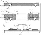
以上を踏まえ、以下では本発明の実施形態を図面を参照しながら説明する。図1は、本発明の一実施形態に係る部品内蔵配線板の構成を模式的に示す断面図(図1(a))およびそのうちの配線層22の一部構成を模式的に示す平面図(図1(b))である。図1に示すように、この部品内蔵配線板は、絶縁層(板状絶縁層)11、同12、同13、同14、同15、配線層(配線パターン)21、同22(ニッケル金属層22bを含む)、同23、同24、同25、同26(=合計6層配線)、層間接続体31、同32、同34、同35、スルーホール導電体33、チップ抵抗41(電気/電子部品)、はんだ接続部材51、はんだレジスト61、62を有する。 Based on the above, embodiments of the present invention will be described below with reference to the drawings. FIG. 1 is a cross-sectional view (FIG. 1A) schematically showing a configuration of a component built-in wiring board according to an embodiment of the present invention, and a plan view schematically showing a partial configuration of a
チップ抵抗41は、例えばその平面的な大きさは例えば0.6mm×0.3mmである。両端に端子(電極)41aを有し、その下側が内層の配線層22が含む内蔵部品実装用ランド(ニッケル金属層22b)に対向位置している。チップ抵抗41の端子41aとニッケル金属層22bとははんだ接続部材51により電気的、機械的に接続されている。はんだ接続部材51は、端子41a周りに形成されたフィレットを含む形状で配線層22のニッケル金属層22b上に位置している。 The
ニッケル金属層22bは、その上に位置するはんだ接続部材51の溶融時の広がりを制限する領域として設けられたニッケルの層である。その厚さは例えば5μm程度とすることができる。平面的には、図1(b)に示すように、例えば、内蔵部品(チップ抵抗41)実装用ランドのうちのはんだ接続部材51が広がるべき制限領域に対応して、配線パターン22の金属箔(後述する)部分を基層としてこの基層上に、位置選択的に形成されている。ニッケル金属層22bにより、はんだ接続部材51の広がりを抑制的にかつ揃ったものにして両端子41aにおけるはんだ接続部材51での応力発生を偏らせず、はんだ接続部材51による電気的接続の信頼性を確保することができる。 The
ニッケル金属層22b上には、製造途上においてはさらに金めっき層が形成されているが(後述する)、はんだ接続の工程を経ることで、金めっき層ははんだ接続部材51が含むすずの中に取り込まれて消失する。このはんだ接続工程において、溶融はんだは、配線パターン22の基層材料である例えば銅と比べて、金との濡れ性の方が大きく良好であるため、上記のような広がり制限の効果を得ることができる。これにより、ニッケル金属層22bの外側の領域には、はんだレジストのような樹脂パターンを設けるには及ばないので、絶縁層12との密着性劣化のおそれはほとんどなく、構造的な信頼性の確保も図ることができる。 A gold plating layer is further formed on the
なお、この実施形態では、はんだ接続部材51の領域を除く配線層22の絶縁層12側の表面は、表面粗さが適度に大きくなるように処理がされた粗化面22aになっている。粗化面22aを設けることで、これを粗化しない場合より、配線層22と絶縁層12との密着性、および層間接続体32との接続信頼性を向上することができる。 In this embodiment, the surface on the insulating
部品内蔵配線板としてのほかの構造について述べると、配線層21、26は、配線板としての両主面上の配線層であり、その上に各種の部品(不図示)が実装され得る。実装ではんだ(不図示)が載るべき配線層21、26のランド部分を除いて両主面上には、はんだ接続時に溶融したはんだをランド部分に留めかつその後は保護層として機能するはんだレジスト61、62が形成されている(厚さはそれぞれ例えば20μm程度)。 Describing another structure as a component built-in wiring board, the wiring layers 21 and 26 are wiring layers on both main surfaces as a wiring board, and various components (not shown) can be mounted thereon. Solder resist 61 is provided on both main surfaces except for the land portions of the wiring layers 21 and 26 on which solder (not shown) is to be mounted in mounting, so that the solder melted at the time of solder connection is held on the land portions and thereafter functions as a protective layer. , 62 (thickness is about 20 μm, for example).
このランド部分の表層には、耐腐食性の高いNi/Auのめっき層(不図示)を形成するようにしてもよい。また、配線層21、26が含むランド上には、はんだボールを設けるような使い方もあり得る。これは、この部品内蔵配線板を別の配線板(例えばマザーボードのような大きな配線板)上に実装するための構成である。 A Ni / Au plating layer (not shown) having high corrosion resistance may be formed on the surface layer of the land portion. Further, there may be a usage in which solder balls are provided on the lands included in the wiring layers 21 and 26. This is a configuration for mounting this component built-in wiring board on another wiring board (for example, a large wiring board such as a mother board).
配線層22、23、24、25は、それぞれ、内層の配線層であり、順に、配線層21と配線層22の間に絶縁層11が、配線層22と配線層23の間に絶縁層12が、配線層23と配線層24との間に絶縁層13が、配線層24と配線層25との間に絶縁層14が、配線層25と配線層26との間に絶縁層15が、それぞれ位置しこれらの配線層21〜26を隔てている。各配線層21〜26は、例えばそれぞれ厚さ18μmの金属(銅)箔からなっている。 The wiring layers 22, 23, 24, and 25 are inner wiring layers, and the insulating
各絶縁層11〜15は、絶縁層13を除き例えばそれぞれ厚さ100μm、絶縁層13のみ例えば厚さ300μmで、それぞれ例えばガラスエポキシ樹脂からなるリジッドな素材である。特に絶縁層13は、内蔵されたチップ抵抗41に相当する位置部分が開口部となっており、チップ抵抗41を内蔵するための空間を提供する。絶縁層12、14は、チップ抵抗41の表面に密着するように絶縁層13の上記開口部および絶縁層13のスルーホール導電体33内部の空間を埋めて変形進入しており内部に空隙となる空間は存在しない。 Each of the insulating
配線層21と配線層22とは、それらのパターンの面の間に挟設されかつ絶縁層11を貫通する層間接続体31により導通し得る。同様に、配線層22と配線層23とは、それらのパターンの面の間に挟設されかつ絶縁層12を貫通する層間接続体32により導通し得る。配線層23と配線層24とは、絶縁層13を貫通して設けられたスルーホール導電体33により導通し得る。配線層24と配線層25とは、それらのパターンの面の間に挟設されかつ絶縁層14を貫通する層間絶縁体34により導通し得る。配線層25と配線層26とは、それらのパターンの面の間に挟設されかつ絶縁層15を貫通する層間接続体35により導通し得る。 The
層間接続体31、32、34、35は、それぞれ、導電性組成物のスクリーン印刷により形成される導電性バンプを由来とするものであり、その製造工程に依拠して軸方向(図1の図示で上下の積層方向)に径が変化している。その直径は、太い側で例えば200μmである。 The
以上、一実施形態に係る部品内蔵配線板の構造について述べた。この部品内蔵配線板では、はんだレジストなどのような層を設けなくても、溶融はんだの濡れ広がりを特定領域に限定して制御でき、はんだ接続部材51の広がりを抑制的にかつ揃ったものにできる。よって、各はんだ接続部材51での応力発生を偏らせず、電気的接続の信頼性を確保できる。また、はんだレジストを設けるに及ばないことから、板状絶縁層11とはんだレジストとの密着性が良好でないことによる剥離を心配する必要がなく、構造的な信頼性の確保も図ることができる。 The structure of the component built-in wiring board according to the embodiment has been described above. In this component built-in wiring board, even without providing a layer such as a solder resist, the spread of the wet solder can be controlled to be limited to a specific region, and the spread of the
次に、図1に示した部品内蔵配線板の製造工程を図2ないし図4を参照して説明する。図2ないし図4は、それぞれ、図1に示した部品内蔵配線板の製造過程の一部を模式的断面で示す工程図である。これらの図において図1中に示した構成要素と同一または同一相当のものには同一符号を付してある。 Next, the manufacturing process of the component built-in wiring board shown in FIG. 1 will be described with reference to FIGS. 2 to 4 are process diagrams schematically showing a part of the manufacturing process of the component built-in wiring board shown in FIG. In these figures, the same or equivalent components as those shown in FIG.
図2から説明する。図2は、図1中に示した各構成のうち絶縁層11を中心とした部分の製造工程を示している。まず、図2(a)に示すように、厚さ例えば18μmの金属箔(電解銅箔)22A上に例えばスクリーン印刷により、層間接続体31となるペースト状の導電性組成物をほぼ円錐形のバンプ状(底面径例えば200μm、高さ例えば160μm)に形成する。この導電性組成物は、ペースト状の樹脂中に銀、金、銅などの金属微細粒または炭素微細粒を分散させたものである。説明の都合で金属箔22Aの下面に印刷しているが上面でもよい(以下の各図も同じである)。層間接続体31の印刷後これを乾燥させて硬化させる。 It demonstrates from FIG. FIG. 2 shows a manufacturing process of a portion centering on the insulating
次に、図2(b)に示すように、金属箔22A上に厚さ例えば公称100μmのFR−4のプリプレグ11Aを積層して層間接続体31を貫通させ、その頭部が露出するようにする。露出に際してあるいはその後その先端を塑性変形でつぶしてもよい(いずれにしても層間接続体31の形状は、積層方向に一致する軸を有しその軸方向に径が変化する形状である。)。続いて、図2(c)に示すように、プリプレグ31A上に金属箔(電解銅箔)21Aを積層配置して加圧・加熱し全体を一体化する。このとき、金属箔21Aは層間接続体31と電気的導通状態となり、プリプレグ11Aは完全に硬化して絶縁層11になる。 Next, as shown in FIG. 2B, an FR-4 prepreg 11A having a thickness of, for example, 100 μm is laminated on the
次に、図2(d)に示すように、片側の金属箔22Aに例えば周知のフォトリソグラフィによるパターニングを施し、これを、実装用ランドを含む配線層22に加工する。加えて、その実装用ランド上に対応して、ニッケルめっき層22b(例えば厚さ5μm;以下、適宜「ニッケル金属層」の代わりに「ニッケルめっき層」という場合がある。)およびその上に金めっき層22c(例えば厚さ0.05μm)をめっき形成する。さらに加えて、配線層22の表面に粗化処理を行って粗化面22aを形成する。 Next, as shown in FIG. 2D, patterning by, for example, well-known photolithography is performed on the
粗化処理として、黒化還元処理やマイクロエッチング処理を採用することができる。マイクロエッチング処理としては、例えば、CZ処理(メック社商品名)やボンドフィルム処理(アトテック社商品名)がある。粗化処理により、配線層22と、この上に積層される絶縁層12との密着性、および層間接続体32との電気的接続の信頼性を向上することができる。 As the roughening treatment, blackening reduction treatment or microetching treatment can be employed. Examples of the micro-etching process include CZ processing (MEC product name) and bond film processing (Atotech product name). By the roughening treatment, the adhesion between the
図2(d)におけるパターニング、めっき形成、粗化処理については、以下のような順序があり得る。めっき層を均質に成長させる意味で粗化前の金属箔22A(または配線パターン22)面上にめっき形成するのが好ましいと考えられる。そこで、めっき形成、粗化処理の順序を維持し、パターニングは、これらの前、中、後の順とする3通りが考えられる。 The patterning, plating formation, and roughening treatment in FIG. 2D can be in the following order. It is considered preferable to form a plating on the surface of the
ここで、めっき形成がパターニングより先の場合には、金属箔22Aを給電路とする、電解めっき工程を含むめっき処理で効率的なめっき形成が可能である。めっき形成がパターニングより後の場合には、無電解めっき工程を用いる。いずれのめっき処理の場合にも、めっき用のレジストマスクを絶縁層11(および金属箔22A上または配線層22上)に形成して、位置選択的にニッケルめっき層22bおよび金めっき層22cの積層金属パターン層が形成され得る。 Here, in the case where the plating is formed before the patterning, efficient plating can be formed by a plating process including an electrolytic plating process using the
図2(d)に示す状態が形成されたら、次に、配線層22の実装用ランド上(すなわち金めっき層22cが形成された領域上)に、図2(e)に示すように、例えばスクリーン印刷によりペースト状はんだ組成物51A(クリームはんだ)を印刷する。ペースト状はんだ組成物51Aは、フラックス中にすずを含むはんだの微細粒(例えばSn−3Ag−0.5Cuのはんだ微細粒、融点は例えば220℃程度)を分散させたものでありスクリーン印刷を用いれば容易に所定パターンに印刷できる。スクリーン印刷に代えてディスペンサを使用することもできる。 When the state shown in FIG. 2D is formed, next, on the mounting land of the wiring layer 22 (that is, on the region where the
ペースト状はんだ組成物51Aの印刷のあと、チップ抵抗41をペースト状はんだ組成物51Aを介して実装用ランド上に例えばマウンタで載置し、さらにその後ペースト状はんだ組成物51Aを例えばリフロー炉でリフローさせる。このリフローで、ペースト状はんだ組成物51Aが含むはんだ微粒子が溶融したとき、銅と比べて比較的濡れ性が高い金めっき22c(ニッケルめっき層22b)上にのみ溶融はんだが広がる。チップ抵抗41のような表面実装型受動素子部品では、はんだによるフィレット形成がうまくいかないことによる実装不良が発生しやすいことから、これを改善する意義が高い。 After printing the
以上説明の工程を経て、図2(f)に示すように、はんだ接続部材51を介してチップ抵抗41がニッケルめっき層22bの実装用ランド上に接続、固定された状態の積層部材1が得られる。この状態では、金めっき層22cは、はんだ接続部材51中に取り込まれて層としてはほぼ消滅おり、はんだ接続部材51とランドとの接触はニッケルめっき層22bが担った状態になる。図2(f)に示す積層部材1を用いる後の工程については図4で後述する。 Through the steps described above, as shown in FIG. 2 (f), the
上記説明の製造工程の変形例として、図2(d)中に示した配線層22表面の粗化処理については、チップ抵抗41の実装の後とすることもできる。チップ抵抗41の実装工程は加熱を伴っているので、配線パターン22の、粗化処理による新生面の露出状態を良好に維持する意味で、粗化処理を実装工程の後とする考えは合理性がある。 As a modification of the manufacturing process described above, the roughening treatment of the surface of the
次に、図3を参照して説明する。図3は、図1中に示した各構成のうち絶縁層13および同12を中心とした部分の製造工程を示している。まず、図3(a)に示すように、両面に例えば厚さ18μmの金属箔(電解銅箔)23A、24Aが積層された例えば厚さ300μmのFR−4の絶縁層13を用意し、その所定位置にスルーホール導電体を形成するための貫通孔72をあけ、かつ内蔵するチップ抵抗41に相当する部分に開口部71を形成する。 Next, a description will be given with reference to FIG. FIG. 3 shows a manufacturing process of a part centering on the insulating
次に、無電解めっきおよび電解めっきを行い、図3(b)に示すように、貫通孔72の内壁にスルーホール導電体33を形成する。このとき開口部71の内壁にも導電体が形成される。さらに、図3(c)に示すように、金属箔23A、24Aを周知のフォトリソグラフィを利用して所定にパターニングして配線層23、24を形成する。配線層23、24のパターニング形成により、開口部71の内壁に形成された導電体も除去される。 Next, electroless plating and electrolytic plating are performed to form a through-
次に、図3(d)に示すように、配線層23上の所定の位置に層間接続体32となる導電性バンプ(底面径例えば200μm、高さ例えば160μm)をペースト状導電性組成物のスクリーン印刷により形成する。続いて、図3(e)に示すように、絶縁層12とすべきFR−4のプリプレグ12A(公称厚さ例えば100μm)を配線層23側にプレス機を用い積層する。プリプレグ12Aには、絶縁層13と同様の、内蔵するチップ抵抗41に相当する部分の開口部をあらかじめ設けておく。 Next, as shown in FIG. 3D, conductive bumps (bottom diameter, for example, 200 μm, height, for example, 160 μm) to be the
この積層工程では、層間接続体32の頭部をプリプレグ12Aに貫通させる。なお、図3(e)における層間接続体32の頭部の破線は、この段階でその頭部を塑性変形させてつぶしておく場合と塑性変形させない場合の両者あり得ることを示す。この工程により、配線層23はプリプレグ12A側に沈み込んで位置することになる。以上により得られた積層部材を積層部材2とする。 In this lamination process, the head of the
以上の図3に示した工程は、以下のような手順とすることも可能である。図3(a)の段階では、貫通孔72のみ形成し内蔵部品用の開口部71を形成せずに続く図3(b)から図3(d)までの工程を行う。次に、図3(e)に相当する工程として、プリプレグ12A(開口のないもの)の積層を行う。そして、絶縁層13およびプリプレグ12Aに部品内蔵用の開口部を同時に形成する、という工程である。 The steps shown in FIG. 3 can be performed as follows. In the stage of FIG. 3A, only the through
次に、図4を参照して説明する。図4は、上記で得られた積層部材1、2などを積層する配置関係を示す図である。ここで、図示上側の積層部材3は、下側の積層部材1と同様な工程を適用し、かつそのあと層間接続体34およびプリプレグ14Aを図示中間の積層部材2における層間接続体32およびプリプレグ12Aと同様にして形成し得られたものである。 Next, a description will be given with reference to FIG. FIG. 4 is a diagram showing an arrangement relationship in which the
ただし、部品(チップ抵抗41)およびこれを接続するための部位(実装用ランド)のない構成であり、さらにプリプレグ14Aにはチップ抵抗41用の開口部も設けない。そのほかは、金属箔(電解銅箔)26A、絶縁層15、層間接続体35、配線層25、プリプレグ14A、層間接続体34とも、それぞれ積層部材1の金属箔21A、絶縁層11、層間接続体31、配線層22、積層部材2のプリプレグ12A、層間接続体32と同じである。 However, there is no component (chip resistor 41) and no part (mounting land) for connecting the component (chip resistor 41), and no opening for the
図4に示すような配置で各積層部材1、2、3を積層配置してプレス機で加圧・加熱する。プレス機での加圧・加熱により、プリプレグ12A、14Aが完全に硬化し全体が積層、一体化する。このとき、加熱により得られるプリプレグ12A、14Aの流動性により、チップ抵抗41の周りの空間およびスルーホール導電体33内部の空間にはプリプレグ12A、14Aが変形進入し空隙は発生しない。また、配線層22、24は、層間接続体32、34にそれぞれ電気的に接続される。 The
図4に示す積層工程の後、上下両面の金属箔26A、21Aを周知のフォトリソグラフィを利用して所定にパターニングし、さらにはんだレジスト61、62の層を形成することにより、図1に示したような部品内蔵配線板を得ることができる。 After the laminating step shown in FIG. 4, the upper and lower metal foils 26A and 21A are patterned in a predetermined manner using well-known photolithography, and further, layers of solder resists 61 and 62 are formed, as shown in FIG. Such a component built-in wiring board can be obtained.
変形例として、中間の絶縁層13に設けられたスルーホール導電体33については、層間接続体31や同32と同様なものとする構成も当然ながらあり得る。また、外側の配線層21、26は、最後の積層工程のあとにパターニングして得る以外に、各積層部材1、3の段階で(例えば図2(d)の段階で)形成するようにしてもよい。 As a modification, the through-
さらに、図4に示した積層工程において、積層部材1、2については、プリプレグ12Aおよび層間接続体32の部分を積層部材2の側ではなく積層部材1の側に設けておくようにしてもよい。すなわち、層間接続体32の形成およびプリプレグ12Aの積層を、積層部材1の配線層22上(絶縁層11上)であらかじめ行うようにする。この場合、実装されたチップ抵抗41が、一見、層間接続体32をスクリーン印刷で形成するときに干渉要因となるように見えるが、チップ抵抗41として十分薄い部品の場合は実際上干渉要因とはならない。プリプレグ12Aの積層工程のときには、チップ抵抗41の厚さを吸収できるクッション材を介在させて加圧・加熱すれば面内方向均一にプリプレグ12Aを積層できる。 Further, in the laminating process shown in FIG. 4, for the
以上説明した実施形態について補足を加える。まず、上記実施形態では、絶縁層11が、絶縁層12との間に配線パターン22を挟むように、配線パターン22上に積層位置している。これによれば、チップ抵抗41aが実装されている配線パターン22は内層配線層のパターンとなり、絶縁層11の外側の面上には別の配線パターン21が設けられ得る。これにより、内蔵のチップ抵抗41aの位置に無関係な配線パターンの形成密度を増加させることができ、パターン設計の自由度が高い部品内蔵配線板とすることができる。 A supplement is added about embodiment described above. First, in the said embodiment, the insulating
また、絶縁層11に設けられた、配線パターン化がされた金属箔(配線層22)を用いて部品実装を行い、その後に、これと別の積層部材2、3との積層プロセスを経てこの実施形態の部品内蔵配線板は得られている。これによる特有の構造として、配線パターン22はニッケル金属層22bをも含めて、絶縁層12の厚み方向に落ち込んで位置することになる。この実施形態は、部品実装が絶縁層11に設けられた配線パターン22上になされ、これは通常の配線板上への部品マウントプロセスと同様、周知かつ容易である。 In addition, component mounting is performed using a metal foil (wiring layer 22) provided with a wiring pattern provided on the insulating
次に、図1に示した部品内蔵配線板に使用の、すずを含むはんだ接続部材51に代えて使用できる別のはんだ接続部材について図5を参照して説明する。図5は、図1に示した部品内蔵配線板に使用のはんだ接続部材51に代えて使用できるはんだ接続部材51aの微細な構造を示す説明図である。はんだ接続部材51aは、図5(a)右側に示すように、微細な構造として、硬化されている樹脂部502A中に導電部505の多孔性構造が形成された構成(樹脂含有はんだ接続部材)になっている。この多孔性構造はその孔の部位に樹脂部502Aが満たされ、空隙をもたせないようにしている。 Next, another solder connection member that can be used in place of the
導電部505は、さらに詳細には、図5(b)に示す拡大断面図に描かれるように、粒子状の金属の種部503Aとこの表面を覆う複数元素系相部513とを有し、種部503Aを覆う複数元素系相部513が互いに連接することによって多孔性構造になっている。なお、はんだ接続部材51a中には、種部503A、複数元素系相部513のほかに、残留はんだ501AAも多少存在する。複数元素系相部513は、はんだ粒子501(図5(a)左側を参照)中のすずと種部503A中の高融点金属とによる合成相であり、はんだ粒子501の融点が240℃以下、複数元素系相部513の融点が260℃以上となるように、はんだ粒子501および種部503A(種粒子503)の材料が選ばれている。 More specifically, the
はんだ接続部材51aの上記微細構造には、それらの形成過程が関連している。概略的には、図5(a)左側に示すように、はんだ接続部材51aは、硬化される前の状態として、ペースト状の絶縁性接着樹脂部502中に、すずを含むはんだ粒子501と高融点金属含有の種粒子503とが分散された構成の組成物である。 Their formation process is related to the fine structure of the solder connection member 51a. Schematically, as shown on the left side of FIG. 5 (a), the solder connection member 51a is in a state before being hardened, in the paste-like insulating
このような導電性接着性樹脂を加熱してはんだ粒子501を溶解させると、そのすず成分と種粒子503が含有する高融点金属とが反応(または溶け合って。以下では「反応」で溶け合う場合も含むこととする)して種粒子503表面が複数元素系相部513に変化し、はんだ粒子501の溶解に由来して複数元素系相部513は互いに連接する。複数元素系相部513が発現するとその融点ははんだ粒子501より高いので、上記加熱の温度程度では固相となって多孔性構造になる。種粒子503のうちの未反応部(中心に近い部位)は、複数元素系相部513の中に種となって残り種部503Aになる。はんだ粒子501のうち複数元素系相部513への変化に残留した分は凝固して残留はんだ501AAになる。 When such a conductive adhesive resin is heated to dissolve the
上記で、はんだ粒子501を溶解させる温度では、絶縁性接着樹脂部502は硬化しないようにその材料が選択されている。これにより、はんだ粒子501が溶解したときのその移動を妨げずに溶解金属と種粒子503との反応が円滑になされるようになっている。このような溶解、反応を生じさせた後に、加熱温度を上げて絶縁性接着樹脂部502を熱硬化させる。この熱硬化により、上記形成された多孔性構造を固定化するように多孔性構造の隙間に樹脂部502Aが満たされた構造ができあがる。 The material is selected so that the insulating
このような構成のはんだ接続部材51aでは、とりわけ、上記導電部505中において複数元素系相部513が連接して形成された多孔性構造がその導電性を担っており、この複数元素系相部513は、上記のように、融点が260℃以上になっている。260℃以上とすることで、この部品内蔵配線板の最外の配線層上に部品実装をするときや、この部品内蔵配線板を別の基板に実装するときの加熱(両者、2次実装時加熱(例えば高くとも250℃))での溶融自体を回避でき、接続不良や短絡をさらに効果的に防止できる利点がある。 In the solder connection member 51a having such a configuration, in particular, a porous structure formed by connecting a plurality of
また、この導電性の多孔性構造は硬化された樹脂部502A中に形成されており、多孔性構造の隙間はこれにより埋められている。したがって、はんだ接続部材51a中にボイドが発生し信頼性が損なわれることがない。さらに、はんだ接続部材51aの導電性が導電体505による多孔性構造によっているので、低抵抗の接続部にすることができる。なお、残留はんだ501AAが2次実装時に再溶融することはあり得るが、複数元素系相部513へ変化せずに残留した分なのでその量はわずかでありかつ樹脂部502A中に閉じ込められているので、信頼性に対する影響は最小限に抑制できる。 In addition, this conductive porous structure is formed in the cured resin portion 502A, and the gap between the porous structures is filled with this. Therefore, voids are not generated in the solder connection member 51a and reliability is not impaired. Furthermore, since the conductivity of the solder connection member 51a is based on the porous structure of the
図6は、図5に示したはんだ接続部材51a中の導電部505を得るための材料の例を示す表であり、図6(a)は、硬化前のはんだ接続部材51aA中に含まれるはんだ粒子501の材料例(すずを含む)、図6(b)は、同じく種粒子503の材料例(高融点金属を含む)である。図6(a)に示すように、これらのはんだ粒子501では、その融点が240℃以下である。はんだ粒子501としてこのような融点の金属材料を用いることで、絶縁層11の耐熱温度までには余裕を持たせることができる。図6(b)に示す組成系または金属は、はんだ粒子501の組成金属であるすずと反応してできる複数元素系相部が融点として260℃以上を有する組成系または金属として選択されている。 FIG. 6 is a table showing an example of a material for obtaining the
図7は、図5に示したはんだ接続部材51aを構成する複数元素系相部513の材料例を示す表であり、図6に示した材料のはんだ粒子501と種粒子503とから形成され得る複数元素系相を示している。図7に示すように、これらの複数元素系相部513は、その融点が260℃以上になっている。このような複数元素系相部513により、2次実装時加熱(例えば高くとも250℃)での再溶融自体が起こらない。 FIG. 7 is a table showing a material example of the
なお、図7に示す複数元素系相におけるx、y(、z)の比は、単純な整数比になる場合(=化学量論的組成;金属間化合物)のみならず、これからはずれて例えばxの値を固定したときにy(、z)が幅をもった値で存在できる場合もある。例えば、固溶体の相の場合や、組成比の異なる2種以上の金属間化合物や固体相が混晶している相(例えば共晶)の場合である。 Note that the ratio of x, y (, z) in the multi-element phase shown in FIG. 7 is not only a simple integer ratio (= stoichiometric composition; intermetallic compound), but deviates from this, for example, x In some cases, y (, z) can exist as a value having a width when the value of is fixed. For example, it is a case of a solid solution phase or a phase in which two or more intermetallic compounds or solid phases having different composition ratios are mixed crystals (for example, a eutectic crystal).
図7に示す複数元素系相における金属間化合物としては、例えば、Cu6Sn5、Ag3Sn、FeSn2、AuSn2が知られている。Cu6Sn5は、これと組成元素が同じで組成比が異なる異種の金属間化合物であるCu3Snと混在して形成される場合があり、この混在比に応じて全体としてx、yの比は単純な整数比ではなくなる。Cu3Snは、Cu6Sn5と比較してもろい性質があるが、その融点が260℃以上であることに変わりはなく、また、導電部505の構造が樹脂部502Aにより補強される構造により、その悪影響を小さく留めることができる。For example, Cu6 Sn5 , Ag3 Sn, FeSn2 , and AuSn2 are known as intermetallic compounds in the multi-element phase shown in FIG. Cu6 Sn5 may be formed in combination with Cu3 Sn, which is a different type of intermetallic compound having the same compositional element and different composition ratio. Depending on this mixture ratio, x and y as a whole may be formed. The ratio is no longer a simple integer ratio. Cu3 Sn has brittle properties compared to Cu6 Sn5 , but its melting point is 260 ° C. or higher, and the structure of the
次に、本発明の別の実施形態に係る部品内蔵配線板について図8を参照して説明する。図8は、本発明の別の実施形態に係る部品内蔵配線板の構成を模式的に示す断面図であり、すでに説明した図中に示した構成要素と同一または同一相当のものには同一符号を付してある。その部位については加える事項がない限り説明を省略する。 Next, a component built-in wiring board according to another embodiment of the present invention will be described with reference to FIG. FIG. 8 is a cross-sectional view schematically showing a configuration of a component built-in wiring board according to another embodiment of the present invention. Components identical or equivalent to those shown in the drawings already described are denoted by the same reference numerals. Is attached. The description of the part is omitted unless there is an additional matter.
この実施形態の部品内蔵配線板の、図1に示した実施形態との違いは、内蔵の部品がチップ抵抗41に代わって、ウエハレベル・チップスケールパッケージによる半導体素子部品42になっていることである。 The difference between the component built-in wiring board of this embodiment and the embodiment shown in FIG. 1 is that the built-in component is a
半導体素子部品42は、半導体チップと、この半導体チップ上に形成されたグリッド状配列の表面実装用端子42aとを少なくとも備えている。表面実装用端子42aは、半導体チップがもともと有する端子パッドから再配線層を介して電気的に導通しつつその位置を再配置して設けられた端子であり、このような再配置により端子としての配置密度が半導体チップ上の端子パッドのそれより粗くなっている。 The
表面実装用端子42aを用い、半導体素子部品42は、表面実装技術で配線層22が含む実装用ランド(すなわちニッケル金属層22b)上にはんだ接続部材55を介して実装され得る。はんだ接続部材55には、上記実施形態におけるはんだ接続部材51と同じ組成のもの、または樹脂含有はんだ接続部材51aと同じものを使用することができる。 Using the surface mounting terminals 42a, the
半導体素子部品42の端子42aの配置ピッチは、例えば0.2mmないし1.0mmである。端子42aが配置された面の中央付近は、半導体素子部品42として必要な端子数が少ない場合は、端子42aが配置されない態様とすることもできる。 The arrangement pitch of the terminals 42a of the
半導体素子部品42は、配線板中に内蔵のため実装される前の形態として、端子42a上にはんだボールのない、いわゆるLGA(land grid array)の形態である。このようなはんだボールのない構成とすることで高さ方向の実装サイズを抑制し、より内蔵への適性を向上させている。内蔵される配線板の厚さが許せば、端子42a上にはんだボールが搭載されたいわゆるBGA(ball grid array)の形態も利用できる。 The
図9は、図8に示した部品内蔵配線板における配線層22の一部構成を模式的に示す平面である。図9において、図8中に示したものと同一相当のものには同一符号を付してある。なお、図8と図9とでは半導体素子部品42の端子数が異なることを前提とする図示であり、これは説明の都合を含む模式的図示のためである。 FIG. 9 is a plan view schematically showing a partial configuration of the
図9に示すように、ニッケル金属層22bは、半導体素子部品42の端子42aとのはんだ接続が必要な領域にのみ形成されている。よって、この実施形態においても、はんだレジストなどのような層を設けなくても、溶融はんだの濡れ広がりをランドの領域に限定して制御でき、はんだ接続部材55の広がりを抑制的にかつ揃ったものにできる。したがって、各はんだ接続部材55での応力発生を偏らせず、電気的接続の信頼性を確保できる。また、はんだレジストを設けるに及ばないことから、絶縁層11とはんだレジストとの密着性が良好でないことによる剥離を心配する必要がなく、構造的な信頼性の確保も図ることができる。 As shown in FIG. 9, the
この実施形態は、図1に示した実施形態と同様に、半導体素子部品42が実装されている内層の配線パターン22とは別に、絶縁層11の外側の面上に配線パターン21が設けられる。これにより、内蔵のチップ抵抗41aの位置に無関係な配線パターンの形成密度を増加させることができ、パターン設計の自由度が高い部品内蔵配線板とすることができる。 In this embodiment, as in the embodiment shown in FIG. 1, the
また、図1に示した実施形態と同様に、部品実装が絶縁層11に設けられた配線パターン22上になされ、これは通常の配線板上への部品マウントプロセスと同様、周知かつ容易である。加えて、半導体素子部品の内蔵により、部品内蔵配線板として、付加価値をより高められる。 Similarly to the embodiment shown in FIG. 1, component mounting is performed on the
次に、本発明のさらに別の実施形態に係る部品内蔵配線板について図10を参照して説明する。図10は、本発明のさらに別の実施形態に係る部品内蔵配線板の構成を模式的に示す断面図(図10(a))およびそのうちの配線層22の一部構成を模式的に示す平面図(図10(b))であり、すでに説明した図中に示した構成要素と同一または同一相当のものには同一符号を付してある。その部位については加える事項がない限り説明を省略する。 Next, a component built-in wiring board according to still another embodiment of the present invention will be described with reference to FIG. FIG. 10 is a cross-sectional view (FIG. 10A) schematically showing a configuration of a component built-in wiring board according to still another embodiment of the present invention, and a plan view schematically showing a partial configuration of the
この実施形態は、配線パターン22が、絶縁層11に接する面と対向する面上には多層化配線構造のない最外配線層のパターンとなっており、これにより、配線層数の増加が限られるが、より薄型の部品内蔵配線板を提供できる。 In this embodiment, the
また、この実施形態では、製造工程に起因して、配線パターン22の基層部分が、絶縁層22の厚み方向に落ち込まずに絶縁層12上に設けられ、一方、配線パターン22のニッケル金属層22bは、絶縁層12の厚み方向に落ち込んで絶縁層12上に設けられている。これは、以下説明するように(図11を参照)、配線パターン化される前の金属箔を用いて部品実装を行い、その後の積層プロセスを経て得られる特有の構造である。配線パターン化される前の金属箔を用いて部品実装を行うことで、より薄型の部品内蔵配線板を製造する工程の全体として、より簡易なプロセスで済む。 Further, in this embodiment, due to the manufacturing process, the base layer portion of the
さらに、この実施形態は、図10(b)に示すように、ニッケル金属層22bが、基層に重ならない位置に設けられたニッケル金属層につながり一体的になっていると言える構造である。これは、部品実装がなされ積層プロセスが終わった状態に対して、金属箔22Aから配線パターン22をパターン形成したときに、ニッケル金属層22bは除去されず基層のみが除去されて導かれ得る構造である。このような構造でも配線として電気的な問題はなく、したがって、配線パターン化の位置精度を、ニッケル金属層22bを含むランド形成の位置精度に対してよりラフに設定することができる。 Further, in this embodiment, as shown in FIG. 10B, the
図11は、図10に示した部品内蔵配線板の製造過程の一部を模式的断面で示す工程図である。図11において、すでに説明した図中に示した構成要素と同一または同一相当のものには同一符号を付してある。その部分については加えるべき事項がない限り説明を省略する。この工程は、図1に示した実施形態で言えば図4に示した最終の積層工程に対応する積層工程である。 FIG. 11 is a process diagram schematically showing a part of the manufacturing process of the component built-in wiring board shown in FIG. In FIG. 11, the same reference numerals are given to the same or equivalent components as those shown in the already described drawings. The description is omitted unless there is a matter to be added. In the embodiment shown in FIG. 1, this process is a lamination process corresponding to the final lamination process shown in FIG.
図4と図11とを比較して分かるように、図11に示す積層工程では、積層部材3に代えて積層部材3Aを用いる。積層部材3Aは、金属箔25A上に層間接続体34を形成し、さらに、層間接続体34の頭部が貫通するように金属箔25A上にプリプレグ14Aを積層した構成である。この構成は、図2(a)、(b)を用いて説明したプロセスで得られる。 As can be seen by comparing FIG. 4 and FIG. 11, in the lamination step shown in FIG. 11, the
また、図11に示す積層工程では、積層部材1に代えて積層部材1Aを用いる。積層部材1Aは、金属箔22A上に、チップ部品41を実装するためのランドとなるニッケルめっき層22b(およびこの段階では不図示要素となる金めっき層)を形成し、このランド上にチップ部品41を実装した構成である。金属箔22A上へのニッケルめっき層22bおよび金めっき層22cの形成は、金属箔22A上にめっき用のレジストマスクを形成し、次に金属箔22Aを給電路とする電解めっき工程を行えば容易にできる。 Further, in the laminating process shown in FIG. 11, the
図11に示す積層工程における作用やその後の工程については、図4での説明と同様である。加えるべきこととして、積層後に金属箔22Aをエッチングして配線パターン22を形成するときには、図10(b)に示したように、ニッケルめっき層22bが一部露出するようなエッチングでも問題はない。 The operations in the stacking step shown in FIG. 11 and the subsequent steps are the same as those described in FIG. As a matter of addition, when the
なお、図11に示す積層工程を経て、両面に配線パターン22、25をエッチング形成して4層配線板を得た後、この4層配線板をコア板に用いて、両面の配線パターン22、25上に多層化配線構造をビルドアップで形成することもできる。ビルドアップの方法の例としては、図2(b)に示すような構成の部材を両面(または片面)に積層する。 In addition, after the lamination process shown in FIG. 11, the
次に、図12は、本発明のさらに別の実施形態に係る部品内蔵配線板の製造過程の一部を模式的断面で示す工程図である。同図において、すでに説明した図中に示した構成要素と同一または同一相当のものには同一符号を付してある。その部分については加えるべき事項がない限り説明を省略する。 Next, FIG. 12 is a process diagram schematically showing a part of the manufacturing process of the component built-in wiring board according to still another embodiment of the present invention. In the figure, the same or equivalent parts as those shown in the already described figures are denoted by the same reference numerals. The description is omitted unless there is a matter to be added.
この実施形態は、図11に示した工程の変形例を用いる、部品実装配線板の製造方法で得られる部品内蔵配線板という位置づけになる。すなわち、この工程では、図11における積層部材1Aに代えて、積層部材1Bを用いる。積層部材1Bは、ステンレス製のダミー板100上に、配線パターン22(粗化面22a、ニッケルめっき層22bあり)、はんだ接続部材51、およびチップ部品41を有する構成を設けた積層部材である。ダミー板100は、図11に示す積層がされた後に取り払われる。 This embodiment is positioned as a component built-in wiring board obtained by a method for manufacturing a component mounting wiring board using a modification of the process shown in FIG. That is, in this step, the laminated member 1B is used instead of the laminated member 1A in FIG. The
この実施形態は、配線パターン22が、絶縁層11に接する面と対向する面上には多層化配線構造のない最外配線層のパターンとなり、これにより、より薄型の部品内蔵配線板を提供できる点は、図10、図11を参照して説明した実施形態と同様である。ただし、構造的には少し異なることになり、図12に示す積層工程に依拠して、配線パターン22の基層部分およびニッケル金属層22bの部分が、両者ともに、絶縁層12の厚み方向に落ち込んで絶縁層12上に設けられることになる。なお、この工程による配線板が、さらに多層配線層化するためのコア板にできる点は、図10、図11での説明と同様である。 In this embodiment, the
積層部材1Bの製造工程について多少補足すると、配線パターン22(その基層部分)は、ダミー板100上に当初積層されていた金属箔22Aを例えば周知のフォトリソグラフィ工程を用いてエッチングしパターニングすることで得ることができる。または、ダミー板100上に、パターン化がされたレジストマスクを形成し、レジストマスクの抜けた部分への電解めっき形成でアディティブに得ることもできる。 If the manufacturing process of the laminated member 1B is somewhat supplemented, the wiring pattern 22 (its base layer portion) is obtained by etching and patterning the
1,1A,1B…積層部材、2…積層部材、3,3A…積層部材、11…絶縁層(板状絶縁層)、11A…プリプレグ、12…絶縁層(板状絶縁層)、12A…プリプレグ、13…絶縁層(板状絶縁層)、14…絶縁層(板状絶縁層)、14A…プリプレグ、15…絶縁層(板状絶縁層)、21…配線層(配線パターン)、21A…金属箔(銅箔)、22…配線層(配線パターン)、22a…粗化面、22b…ニッケル金属層(ニッケルめっき層)、22c…金めっき層、22A…金属箔(銅箔)、23…配線層(配線パターン)、23A…金属箔(銅箔)、24…配線層(配線パターン)、24A…金属箔(銅箔)、25…配線層(配線パターン)、25A…金属箔(銅箔)、26…配線層(配線パターン)、26A…金属箔(銅箔)、31,32,34,35…層間接続体(導電性組成物印刷による導電性バンプ)、33…スルーホール導電体、41…チップ抵抗(電気/電子部品)、41a…端子、42…半導体素子部品(ウエハレベル・チップスケールパッケージによる電気/電子部品)、42a…表面実装用端子、51,55…はんだ接続部材、51A…ペースト状はんだ組成物、51a…樹脂含有はんだ接続部材、51aA…樹脂含有はんだ接続部材(硬化前;ペースト状はんだ組成物)、61,62…はんだレジスト、71…部品用開口部、72…貫通孔、81,82…開口部、100…ダミー板(ステンレス板)、501…はんだ粒子、501AA…残留はんだ、502…絶縁性接着樹脂部(硬化前)、502A…絶縁性接着樹脂部(硬化後)、503…種粒子、503A…種部、505…多孔性構造導電部(種部と複数元素系相部とによる)、513…複数元素系相部。 1, 1A, 1B ... laminated member, 2 ... laminated member, 3, 3A ... laminated member, 11 ... insulating layer (plate-like insulating layer), 11A ... prepreg, 12 ... insulating layer (plate-like insulating layer), 12A ... prepreg , 13 ... insulating layer (plate-like insulating layer), 14 ... insulating layer (plate-like insulating layer), 14A ... prepreg, 15 ... insulating layer (plate-like insulating layer), 21 ... wiring layer (wiring pattern), 21A ... metal Foil (copper foil), 22 ... wiring layer (wiring pattern), 22a ... roughened surface, 22b ... nickel metal layer (nickel plating layer), 22c ... gold plating layer, 22A ... metal foil (copper foil), 23 ... wiring Layer (wiring pattern), 23A ... Metal foil (copper foil), 24 ... Wiring layer (wiring pattern), 24A ... Metal foil (copper foil), 25 ... Wiring layer (wiring pattern), 25A ... Metal foil (copper foil) 26 ... wiring layer (wiring pattern), 26A ... metal foil (copper foil), 3 , 32, 34, 35... Interlayer connection body (conductive bump by conductive composition printing), 33... Through-hole conductor, 41... Chip resistor (electric / electronic component), 41 a. Wafer level / chip scale package electrical / electronic components), 42a ... surface mounting terminals, 51, 55 ... solder connection member, 51A ... paste solder composition, 51a ... resin-containing solder connection member, 51aA ... resin-containing solder connection Member (before curing; paste solder composition), 61, 62 ... solder resist, 71 ... opening for parts, 72 ... through hole, 81, 82 ... opening, 100 ... dummy plate (stainless steel plate), 501 ... solder Particles, 501AA ... residual solder, 502 ... insulating adhesive resin part (before curing), 502A ... insulating adhesive resin part (after curing), 503 ... seed particles, 03A ... seed unit, 505 ... (according to the species part and multi-element system phase portion) porous structure conductive portion, 513 ... multiple element system phase portion.
Claims (11)
Translated fromJapanese前記電気/電子部品の表面の少なくとも一部に密着して該電気/電子部品の少なくとも一部分を埋め込んだ板状絶縁層と、
前記板状絶縁層の上面上に設けられた第1の配線パターンと、
前記板状絶縁層の前記上面に対向する下面上に設けられた、前記電気/電子部品の実装用のランドを含む第2の配線パターンと、
前記電気/電子部品の前記端子と前記第2の配線パターンの前記ランドとを電気的、機械的に接続する、すずおよび金を含むはんだ接続部材と、を具備し、
前記第2の配線パターンが、基層と、該基層上位置選択的に積層された、前記はんだ接続部材と該基層との間に挟まれて位置するニッケル金属層とを有すること
を特徴とする部品内蔵配線板。An electrical / electronic component having a terminal;
A plate-like insulating layer in close contact with at least a part of the surface of the electric / electronic component and embedding at least a part of the electric / electronic component;
A first wiring pattern provided on the upper surface of the plate-like insulating layer;
A second wiring pattern including a land for mounting the electric / electronic component provided on a lower surface of the plate-like insulating layer facing the upper surface;
A solder connection member including tin and gold for electrically and mechanically connecting the terminal of the electrical / electronic component and the land of the second wiring pattern;
The second wiring pattern includes a base layer and a nickel metal layer that is selectively stacked on the base layer and positioned between the solder connection member and the base layer. Built-in wiring board.
前記導電部が、高融点金属の粒子の種部と、該種部を覆った、前記高融点金属とすずとの複数元素系相部とを含有し、かつ、該複数元素系相部が連接して前記多孔性の構造を形成しており、前記導電部が、すずを組成のひとつとするはんだ成分をさらに含有し、該はんだ成分の融点が240℃以下であり、前記複数元素系相部の融点が260℃以上であること
を特徴とする請求項1記載の部品内蔵配線板。The solder connection member has a conductive portion having a porous structure, and a resin portion that is buried between the porous structures of the conductive portion,
The conductive part includes a seed part of a refractory metal particle, and a multi-element phase part of the refractory metal and tin covering the seed part, and the multi-element phase part is connected Forming the porous structure, and the conductive part further contains a solder component having a composition of tin, the melting point of the solder component being 240 ° C. or less, and the multi-element phase part The component built-in wiring board according to claim 1, wherein the melting point of the component is 260 ° C. or higher.
前記積層金属パターン層上にすずを含むはんだ成分を含有のペースト状はんだ組成物を付着させる工程と、
前記ペースト状はんだ組成物を介した前記積層金属パターン層上に電気/電子部品をマウントする工程と、
前記ペースト状はんだ組成物をリフローさせ前記電気/電子部品を前記積層金属パターン層上に固定する工程と、
前記電気/電子部品の表面に密着して該電気/電子部品を埋め込むように、配線パターン化される前の前記金属箔上または配線パターン化がされた前記金属箔上に、板状絶縁層を積層する工程と
を具備することを特徴とする部品内蔵配線板の製造方法。On the metal foil before the wiring pattern is formed or on the metal foil on which the wiring pattern is formed, on the nickel plating layer and the nickel plating layer for selectively forming a land for mounting electric / electronic components. Plating a laminated metal pattern layer having a gold plating layer positioned; and
Attaching a solder paste containing a solder component containing tin on the laminated metal pattern layer; and
Mounting an electrical / electronic component on the laminated metal pattern layer via the paste solder composition;
Reflowing the paste solder composition and fixing the electric / electronic component on the laminated metal pattern layer;
A plate-like insulating layer is formed on the metal foil before the wiring patterning or on the metal foil on which the wiring pattern has been formed so that the electric / electronic component is embedded in close contact with the surface of the electric / electronic component. And a laminating step. A method of manufacturing a component built-in wiring board.
Priority Applications (1)
| Application Number | Priority Date | Filing Date | Title |
|---|---|---|---|
| JP2010095856AJP2011228422A (en) | 2010-04-19 | 2010-04-19 | Wiring board incorporating components, and method of manufacturing the same |
Applications Claiming Priority (1)
| Application Number | Priority Date | Filing Date | Title |
|---|---|---|---|
| JP2010095856AJP2011228422A (en) | 2010-04-19 | 2010-04-19 | Wiring board incorporating components, and method of manufacturing the same |
Publications (1)
| Publication Number | Publication Date |
|---|---|
| JP2011228422Atrue JP2011228422A (en) | 2011-11-10 |
Family
ID=45043462
Family Applications (1)
| Application Number | Title | Priority Date | Filing Date |
|---|---|---|---|
| JP2010095856APendingJP2011228422A (en) | 2010-04-19 | 2010-04-19 | Wiring board incorporating components, and method of manufacturing the same |
Country Status (1)
| Country | Link |
|---|---|
| JP (1) | JP2011228422A (en) |
Cited By (2)
| Publication number | Priority date | Publication date | Assignee | Title |
|---|---|---|---|---|
| CN113013112A (en)* | 2021-02-19 | 2021-06-22 | 日月光半导体制造股份有限公司 | Semiconductor structure and manufacturing method thereof |
| WO2024142884A1 (en)* | 2022-12-28 | 2024-07-04 | ローム株式会社 | Electronic device and method for manufacturing electronic device |
Citations (6)
| Publication number | Priority date | Publication date | Assignee | Title |
|---|---|---|---|---|
| JP2006093271A (en)* | 2004-09-22 | 2006-04-06 | Toppan Printing Co Ltd | Wiring board manufacturing method |
| JP2008244191A (en)* | 2007-03-28 | 2008-10-09 | Fujitsu Ltd | Manufacturing method of component-embedded substrate |
| WO2009001621A1 (en)* | 2007-06-26 | 2008-12-31 | Murata Manufacturing Co., Ltd. | Manufacturing method for part built-in substrate |
| JP2009253261A (en)* | 2008-04-07 | 2009-10-29 | Samsung Electro Mech Co Ltd | High density circuit board and manufacturing method thereof |
| JP2009267149A (en)* | 2008-04-25 | 2009-11-12 | Dainippon Printing Co Ltd | Part built-in wiring board, and method for manufacturing part built-in wiring board |
| JP2010010671A (en)* | 2008-05-29 | 2010-01-14 | Dainippon Printing Co Ltd | Wiring board with built-in component, and method of manufacturing wiring board with built-in component |
- 2010
- 2010-04-19JPJP2010095856Apatent/JP2011228422A/enactivePending
Patent Citations (6)
| Publication number | Priority date | Publication date | Assignee | Title |
|---|---|---|---|---|
| JP2006093271A (en)* | 2004-09-22 | 2006-04-06 | Toppan Printing Co Ltd | Wiring board manufacturing method |
| JP2008244191A (en)* | 2007-03-28 | 2008-10-09 | Fujitsu Ltd | Manufacturing method of component-embedded substrate |
| WO2009001621A1 (en)* | 2007-06-26 | 2008-12-31 | Murata Manufacturing Co., Ltd. | Manufacturing method for part built-in substrate |
| JP2009253261A (en)* | 2008-04-07 | 2009-10-29 | Samsung Electro Mech Co Ltd | High density circuit board and manufacturing method thereof |
| JP2009267149A (en)* | 2008-04-25 | 2009-11-12 | Dainippon Printing Co Ltd | Part built-in wiring board, and method for manufacturing part built-in wiring board |
| JP2010010671A (en)* | 2008-05-29 | 2010-01-14 | Dainippon Printing Co Ltd | Wiring board with built-in component, and method of manufacturing wiring board with built-in component |
Cited By (2)
| Publication number | Priority date | Publication date | Assignee | Title |
|---|---|---|---|---|
| CN113013112A (en)* | 2021-02-19 | 2021-06-22 | 日月光半导体制造股份有限公司 | Semiconductor structure and manufacturing method thereof |
| WO2024142884A1 (en)* | 2022-12-28 | 2024-07-04 | ローム株式会社 | Electronic device and method for manufacturing electronic device |
Similar Documents
| Publication | Publication Date | Title |
|---|---|---|
| TWI545998B (en) | Built-in parts wiring board | |
| JP5130661B2 (en) | Component built-in wiring board, manufacturing method of component built-in wiring board. | |
| JP5851079B2 (en) | Component built-in wiring board | |
| JP2010010671A (en) | Wiring board with built-in component, and method of manufacturing wiring board with built-in component | |
| JP2011134957A (en) | Multilayer wiring board | |
| JP2017084997A (en) | Printed wiring board and method of manufacturing the same | |
| JP4945974B2 (en) | Component built-in wiring board | |
| JP2009252942A (en) | Component built-in wiring board, and method of manufacturing component built-in wiring board | |
| JP2009267149A (en) | Part built-in wiring board, and method for manufacturing part built-in wiring board | |
| JP2014179430A (en) | Multilayer printed wiring board for mounting semiconductor element | |
| JP5397012B2 (en) | Component built-in wiring board, method of manufacturing component built-in wiring board | |
| JP2009111307A (en) | Component built-in wiring board | |
| JP5108253B2 (en) | Component mounting module | |
| JP2008177619A (en) | Chip carrier, semiconductor device, and chip carrier manufacturing method | |
| JP2011228422A (en) | Wiring board incorporating components, and method of manufacturing the same | |
| JP2011249457A (en) | Wiring board having embedded component, and manufacturing method for the same | |
| JP5130666B2 (en) | Component built-in wiring board | |
| JP5359993B2 (en) | Component built-in wiring board, method of manufacturing component built-in wiring board | |
| JP4065264B2 (en) | Substrate with relay substrate and method for manufacturing the same | |
| JP2013077726A (en) | Method of manufacturing semiconductor package | |
| JP5601413B2 (en) | Component built-in wiring board, method of manufacturing component built-in wiring board | |
| JP2011071560A (en) | Manufacturing method of component built-in wiring board | |
| JP5895981B2 (en) | Electronic module | |
| JP5733378B2 (en) | Component built-in wiring board, method of manufacturing component built-in wiring board | |
| JP5818296B2 (en) | Electronic module and method for manufacturing electronic module |
Legal Events
| Date | Code | Title | Description |
|---|---|---|---|
| A621 | Written request for application examination | Free format text:JAPANESE INTERMEDIATE CODE: A621 Effective date:20130214 | |
| A977 | Report on retrieval | Free format text:JAPANESE INTERMEDIATE CODE: A971007 Effective date:20131004 | |
| A131 | Notification of reasons for refusal | Free format text:JAPANESE INTERMEDIATE CODE: A131 Effective date:20131015 | |
| A521 | Written amendment | Free format text:JAPANESE INTERMEDIATE CODE: A523 Effective date:20131212 | |
| A131 | Notification of reasons for refusal | Free format text:JAPANESE INTERMEDIATE CODE: A131 Effective date:20140318 | |
| A521 | Written amendment | Free format text:JAPANESE INTERMEDIATE CODE: A523 Effective date:20140515 | |
| A02 | Decision of refusal | Free format text:JAPANESE INTERMEDIATE CODE: A02 Effective date:20140701 |