JP2011222707A - Power semiconductor device - Google Patents
Power semiconductor deviceDownload PDFInfo
- Publication number
- JP2011222707A JP2011222707AJP2010089585AJP2010089585AJP2011222707AJP 2011222707 AJP2011222707 AJP 2011222707AJP 2010089585 AJP2010089585 AJP 2010089585AJP 2010089585 AJP2010089585 AJP 2010089585AJP 2011222707 AJP2011222707 AJP 2011222707A
- Authority
- JP
- Japan
- Prior art keywords
- power semiconductor
- connection member
- pattern
- metal wire
- semiconductor device
- Prior art date
- Legal status (The legal status is an assumption and is not a legal conclusion. Google has not performed a legal analysis and makes no representation as to the accuracy of the status listed.)
- Pending
Links
Images


Classifications
- H—ELECTRICITY
- H01—ELECTRIC ELEMENTS
- H01L—SEMICONDUCTOR DEVICES NOT COVERED BY CLASS H10
- H01L24/00—Arrangements for connecting or disconnecting semiconductor or solid-state bodies; Methods or apparatus related thereto
- H01L24/73—Means for bonding being of different types provided for in two or more of groups H01L24/10, H01L24/18, H01L24/26, H01L24/34, H01L24/42, H01L24/50, H01L24/63, H01L24/71
- H—ELECTRICITY
- H01—ELECTRIC ELEMENTS
- H01L—SEMICONDUCTOR DEVICES NOT COVERED BY CLASS H10
- H01L24/00—Arrangements for connecting or disconnecting semiconductor or solid-state bodies; Methods or apparatus related thereto
- H01L24/01—Means for bonding being attached to, or being formed on, the surface to be connected, e.g. chip-to-package, die-attach, "first-level" interconnects; Manufacturing methods related thereto
- H01L24/34—Strap connectors, e.g. copper straps for grounding power devices; Manufacturing methods related thereto
- H01L24/36—Structure, shape, material or disposition of the strap connectors prior to the connecting process
- H01L24/37—Structure, shape, material or disposition of the strap connectors prior to the connecting process of an individual strap connector
- H—ELECTRICITY
- H01—ELECTRIC ELEMENTS
- H01L—SEMICONDUCTOR DEVICES NOT COVERED BY CLASS H10
- H01L2224/00—Indexing scheme for arrangements for connecting or disconnecting semiconductor or solid-state bodies and methods related thereto as covered by H01L24/00
- H01L2224/01—Means for bonding being attached to, or being formed on, the surface to be connected, e.g. chip-to-package, die-attach, "first-level" interconnects; Manufacturing methods related thereto
- H01L2224/02—Bonding areas; Manufacturing methods related thereto
- H01L2224/04—Structure, shape, material or disposition of the bonding areas prior to the connecting process
- H01L2224/06—Structure, shape, material or disposition of the bonding areas prior to the connecting process of a plurality of bonding areas
- H01L2224/0601—Structure
- H01L2224/0603—Bonding areas having different sizes, e.g. different heights or widths
- H—ELECTRICITY
- H01—ELECTRIC ELEMENTS
- H01L—SEMICONDUCTOR DEVICES NOT COVERED BY CLASS H10
- H01L2224/00—Indexing scheme for arrangements for connecting or disconnecting semiconductor or solid-state bodies and methods related thereto as covered by H01L24/00
- H01L2224/01—Means for bonding being attached to, or being formed on, the surface to be connected, e.g. chip-to-package, die-attach, "first-level" interconnects; Manufacturing methods related thereto
- H01L2224/26—Layer connectors, e.g. plate connectors, solder or adhesive layers; Manufacturing methods related thereto
- H01L2224/31—Structure, shape, material or disposition of the layer connectors after the connecting process
- H01L2224/32—Structure, shape, material or disposition of the layer connectors after the connecting process of an individual layer connector
- H01L2224/321—Disposition
- H01L2224/32151—Disposition the layer connector connecting between a semiconductor or solid-state body and an item not being a semiconductor or solid-state body, e.g. chip-to-substrate, chip-to-passive
- H01L2224/32221—Disposition the layer connector connecting between a semiconductor or solid-state body and an item not being a semiconductor or solid-state body, e.g. chip-to-substrate, chip-to-passive the body and the item being stacked
- H01L2224/32225—Disposition the layer connector connecting between a semiconductor or solid-state body and an item not being a semiconductor or solid-state body, e.g. chip-to-substrate, chip-to-passive the body and the item being stacked the item being non-metallic, e.g. insulating substrate with or without metallisation
- H—ELECTRICITY
- H01—ELECTRIC ELEMENTS
- H01L—SEMICONDUCTOR DEVICES NOT COVERED BY CLASS H10
- H01L2224/00—Indexing scheme for arrangements for connecting or disconnecting semiconductor or solid-state bodies and methods related thereto as covered by H01L24/00
- H01L2224/01—Means for bonding being attached to, or being formed on, the surface to be connected, e.g. chip-to-package, die-attach, "first-level" interconnects; Manufacturing methods related thereto
- H01L2224/34—Strap connectors, e.g. copper straps for grounding power devices; Manufacturing methods related thereto
- H01L2224/36—Structure, shape, material or disposition of the strap connectors prior to the connecting process
- H01L2224/37—Structure, shape, material or disposition of the strap connectors prior to the connecting process of an individual strap connector
- H01L2224/37001—Core members of the connector
- H01L2224/37099—Material
- H01L2224/371—Material with a principal constituent of the material being a metal or a metalloid, e.g. boron [B], silicon [Si], germanium [Ge], arsenic [As], antimony [Sb], tellurium [Te] and polonium [Po], and alloys thereof
- H01L2224/37117—Material with a principal constituent of the material being a metal or a metalloid, e.g. boron [B], silicon [Si], germanium [Ge], arsenic [As], antimony [Sb], tellurium [Te] and polonium [Po], and alloys thereof the principal constituent melting at a temperature of greater than or equal to 400°C and less than 950°C
- H01L2224/37124—Aluminium [Al] as principal constituent
- H—ELECTRICITY
- H01—ELECTRIC ELEMENTS
- H01L—SEMICONDUCTOR DEVICES NOT COVERED BY CLASS H10
- H01L2224/00—Indexing scheme for arrangements for connecting or disconnecting semiconductor or solid-state bodies and methods related thereto as covered by H01L24/00
- H01L2224/01—Means for bonding being attached to, or being formed on, the surface to be connected, e.g. chip-to-package, die-attach, "first-level" interconnects; Manufacturing methods related thereto
- H01L2224/34—Strap connectors, e.g. copper straps for grounding power devices; Manufacturing methods related thereto
- H01L2224/36—Structure, shape, material or disposition of the strap connectors prior to the connecting process
- H01L2224/37—Structure, shape, material or disposition of the strap connectors prior to the connecting process of an individual strap connector
- H01L2224/37001—Core members of the connector
- H01L2224/37099—Material
- H01L2224/371—Material with a principal constituent of the material being a metal or a metalloid, e.g. boron [B], silicon [Si], germanium [Ge], arsenic [As], antimony [Sb], tellurium [Te] and polonium [Po], and alloys thereof
- H01L2224/37138—Material with a principal constituent of the material being a metal or a metalloid, e.g. boron [B], silicon [Si], germanium [Ge], arsenic [As], antimony [Sb], tellurium [Te] and polonium [Po], and alloys thereof the principal constituent melting at a temperature of greater than or equal to 950°C and less than 1550°C
- H01L2224/37144—Gold [Au] as principal constituent
- H—ELECTRICITY
- H01—ELECTRIC ELEMENTS
- H01L—SEMICONDUCTOR DEVICES NOT COVERED BY CLASS H10
- H01L2224/00—Indexing scheme for arrangements for connecting or disconnecting semiconductor or solid-state bodies and methods related thereto as covered by H01L24/00
- H01L2224/01—Means for bonding being attached to, or being formed on, the surface to be connected, e.g. chip-to-package, die-attach, "first-level" interconnects; Manufacturing methods related thereto
- H01L2224/34—Strap connectors, e.g. copper straps for grounding power devices; Manufacturing methods related thereto
- H01L2224/36—Structure, shape, material or disposition of the strap connectors prior to the connecting process
- H01L2224/37—Structure, shape, material or disposition of the strap connectors prior to the connecting process of an individual strap connector
- H01L2224/37001—Core members of the connector
- H01L2224/37099—Material
- H01L2224/371—Material with a principal constituent of the material being a metal or a metalloid, e.g. boron [B], silicon [Si], germanium [Ge], arsenic [As], antimony [Sb], tellurium [Te] and polonium [Po], and alloys thereof
- H01L2224/37138—Material with a principal constituent of the material being a metal or a metalloid, e.g. boron [B], silicon [Si], germanium [Ge], arsenic [As], antimony [Sb], tellurium [Te] and polonium [Po], and alloys thereof the principal constituent melting at a temperature of greater than or equal to 950°C and less than 1550°C
- H01L2224/37147—Copper [Cu] as principal constituent
- H—ELECTRICITY
- H01—ELECTRIC ELEMENTS
- H01L—SEMICONDUCTOR DEVICES NOT COVERED BY CLASS H10
- H01L2224/00—Indexing scheme for arrangements for connecting or disconnecting semiconductor or solid-state bodies and methods related thereto as covered by H01L24/00
- H01L2224/01—Means for bonding being attached to, or being formed on, the surface to be connected, e.g. chip-to-package, die-attach, "first-level" interconnects; Manufacturing methods related thereto
- H01L2224/34—Strap connectors, e.g. copper straps for grounding power devices; Manufacturing methods related thereto
- H01L2224/39—Structure, shape, material or disposition of the strap connectors after the connecting process
- H01L2224/40—Structure, shape, material or disposition of the strap connectors after the connecting process of an individual strap connector
- H01L2224/4005—Shape
- H01L2224/4009—Loop shape
- H01L2224/40095—Kinked
- H—ELECTRICITY
- H01—ELECTRIC ELEMENTS
- H01L—SEMICONDUCTOR DEVICES NOT COVERED BY CLASS H10
- H01L2224/00—Indexing scheme for arrangements for connecting or disconnecting semiconductor or solid-state bodies and methods related thereto as covered by H01L24/00
- H01L2224/01—Means for bonding being attached to, or being formed on, the surface to be connected, e.g. chip-to-package, die-attach, "first-level" interconnects; Manufacturing methods related thereto
- H01L2224/34—Strap connectors, e.g. copper straps for grounding power devices; Manufacturing methods related thereto
- H01L2224/39—Structure, shape, material or disposition of the strap connectors after the connecting process
- H01L2224/40—Structure, shape, material or disposition of the strap connectors after the connecting process of an individual strap connector
- H01L2224/401—Disposition
- H01L2224/40151—Connecting between a semiconductor or solid-state body and an item not being a semiconductor or solid-state body, e.g. chip-to-substrate, chip-to-passive
- H01L2224/40221—Connecting between a semiconductor or solid-state body and an item not being a semiconductor or solid-state body, e.g. chip-to-substrate, chip-to-passive the body and the item being stacked
- H01L2224/40225—Connecting between a semiconductor or solid-state body and an item not being a semiconductor or solid-state body, e.g. chip-to-substrate, chip-to-passive the body and the item being stacked the item being non-metallic, e.g. insulating substrate with or without metallisation
- H01L2224/40227—Connecting the strap to a bond pad of the item
- H—ELECTRICITY
- H01—ELECTRIC ELEMENTS
- H01L—SEMICONDUCTOR DEVICES NOT COVERED BY CLASS H10
- H01L2224/00—Indexing scheme for arrangements for connecting or disconnecting semiconductor or solid-state bodies and methods related thereto as covered by H01L24/00
- H01L2224/01—Means for bonding being attached to, or being formed on, the surface to be connected, e.g. chip-to-package, die-attach, "first-level" interconnects; Manufacturing methods related thereto
- H01L2224/42—Wire connectors; Manufacturing methods related thereto
- H01L2224/47—Structure, shape, material or disposition of the wire connectors after the connecting process
- H01L2224/48—Structure, shape, material or disposition of the wire connectors after the connecting process of an individual wire connector
- H01L2224/4805—Shape
- H01L2224/4809—Loop shape
- H01L2224/48091—Arched
- H—ELECTRICITY
- H01—ELECTRIC ELEMENTS
- H01L—SEMICONDUCTOR DEVICES NOT COVERED BY CLASS H10
- H01L2224/00—Indexing scheme for arrangements for connecting or disconnecting semiconductor or solid-state bodies and methods related thereto as covered by H01L24/00
- H01L2224/01—Means for bonding being attached to, or being formed on, the surface to be connected, e.g. chip-to-package, die-attach, "first-level" interconnects; Manufacturing methods related thereto
- H01L2224/42—Wire connectors; Manufacturing methods related thereto
- H01L2224/47—Structure, shape, material or disposition of the wire connectors after the connecting process
- H01L2224/48—Structure, shape, material or disposition of the wire connectors after the connecting process of an individual wire connector
- H01L2224/481—Disposition
- H01L2224/48151—Connecting between a semiconductor or solid-state body and an item not being a semiconductor or solid-state body, e.g. chip-to-substrate, chip-to-passive
- H01L2224/48221—Connecting between a semiconductor or solid-state body and an item not being a semiconductor or solid-state body, e.g. chip-to-substrate, chip-to-passive the body and the item being stacked
- H01L2224/48225—Connecting between a semiconductor or solid-state body and an item not being a semiconductor or solid-state body, e.g. chip-to-substrate, chip-to-passive the body and the item being stacked the item being non-metallic, e.g. insulating substrate with or without metallisation
- H01L2224/48227—Connecting between a semiconductor or solid-state body and an item not being a semiconductor or solid-state body, e.g. chip-to-substrate, chip-to-passive the body and the item being stacked the item being non-metallic, e.g. insulating substrate with or without metallisation connecting the wire to a bond pad of the item
- H—ELECTRICITY
- H01—ELECTRIC ELEMENTS
- H01L—SEMICONDUCTOR DEVICES NOT COVERED BY CLASS H10
- H01L2224/00—Indexing scheme for arrangements for connecting or disconnecting semiconductor or solid-state bodies and methods related thereto as covered by H01L24/00
- H01L2224/01—Means for bonding being attached to, or being formed on, the surface to be connected, e.g. chip-to-package, die-attach, "first-level" interconnects; Manufacturing methods related thereto
- H01L2224/42—Wire connectors; Manufacturing methods related thereto
- H01L2224/47—Structure, shape, material or disposition of the wire connectors after the connecting process
- H01L2224/49—Structure, shape, material or disposition of the wire connectors after the connecting process of a plurality of wire connectors
- H01L2224/491—Disposition
- H01L2224/4911—Disposition the connectors being bonded to at least one common bonding area, e.g. daisy chain
- H01L2224/49111—Disposition the connectors being bonded to at least one common bonding area, e.g. daisy chain the connectors connecting two common bonding areas, e.g. Litz or braid wires
- H—ELECTRICITY
- H01—ELECTRIC ELEMENTS
- H01L—SEMICONDUCTOR DEVICES NOT COVERED BY CLASS H10
- H01L2224/00—Indexing scheme for arrangements for connecting or disconnecting semiconductor or solid-state bodies and methods related thereto as covered by H01L24/00
- H01L2224/73—Means for bonding being of different types provided for in two or more of groups H01L2224/10, H01L2224/18, H01L2224/26, H01L2224/34, H01L2224/42, H01L2224/50, H01L2224/63, H01L2224/71
- H01L2224/732—Location after the connecting process
- H01L2224/73201—Location after the connecting process on the same surface
- H01L2224/73221—Strap and wire connectors
- H—ELECTRICITY
- H01—ELECTRIC ELEMENTS
- H01L—SEMICONDUCTOR DEVICES NOT COVERED BY CLASS H10
- H01L2224/00—Indexing scheme for arrangements for connecting or disconnecting semiconductor or solid-state bodies and methods related thereto as covered by H01L24/00
- H01L2224/73—Means for bonding being of different types provided for in two or more of groups H01L2224/10, H01L2224/18, H01L2224/26, H01L2224/34, H01L2224/42, H01L2224/50, H01L2224/63, H01L2224/71
- H01L2224/732—Location after the connecting process
- H01L2224/73251—Location after the connecting process on different surfaces
- H01L2224/73265—Layer and wire connectors
- H—ELECTRICITY
- H01—ELECTRIC ELEMENTS
- H01L—SEMICONDUCTOR DEVICES NOT COVERED BY CLASS H10
- H01L2224/00—Indexing scheme for arrangements for connecting or disconnecting semiconductor or solid-state bodies and methods related thereto as covered by H01L24/00
- H01L2224/80—Methods for connecting semiconductor or other solid state bodies using means for bonding being attached to, or being formed on, the surface to be connected
- H01L2224/84—Methods for connecting semiconductor or other solid state bodies using means for bonding being attached to, or being formed on, the surface to be connected using a strap connector
- H01L2224/848—Bonding techniques
- H01L2224/84801—Soldering or alloying
- H—ELECTRICITY
- H01—ELECTRIC ELEMENTS
- H01L—SEMICONDUCTOR DEVICES NOT COVERED BY CLASS H10
- H01L2924/00—Indexing scheme for arrangements or methods for connecting or disconnecting semiconductor or solid-state bodies as covered by H01L24/00
- H01L2924/10—Details of semiconductor or other solid state devices to be connected
- H01L2924/11—Device type
- H01L2924/13—Discrete devices, e.g. 3 terminal devices
- H01L2924/1304—Transistor
- H01L2924/1305—Bipolar Junction Transistor [BJT]
- H01L2924/13055—Insulated gate bipolar transistor [IGBT]
- H—ELECTRICITY
- H01—ELECTRIC ELEMENTS
- H01L—SEMICONDUCTOR DEVICES NOT COVERED BY CLASS H10
- H01L2924/00—Indexing scheme for arrangements or methods for connecting or disconnecting semiconductor or solid-state bodies as covered by H01L24/00
- H01L2924/10—Details of semiconductor or other solid state devices to be connected
- H01L2924/11—Device type
- H01L2924/13—Discrete devices, e.g. 3 terminal devices
- H01L2924/1304—Transistor
- H01L2924/1306—Field-effect transistor [FET]
- H01L2924/13091—Metal-Oxide-Semiconductor Field-Effect Transistor [MOSFET]
Landscapes
- Engineering & Computer Science (AREA)
- Computer Hardware Design (AREA)
- Microelectronics & Electronic Packaging (AREA)
- Power Engineering (AREA)
- Cooling Or The Like Of Semiconductors Or Solid State Devices (AREA)
Abstract
Translated fromJapaneseDescription
Translated fromJapanese本発明は、絶縁基板上に電力用半導体素子が実装された電力用半導体装置に関し、特にワイヤ接合部の寿命を向上させることができる電力用半導体装置に関する。 The present invention relates to a power semiconductor device in which a power semiconductor element is mounted on an insulating substrate, and more particularly to a power semiconductor device capable of improving the life of a wire junction.
近年、絶縁基板上に電力用半導体素子が実装された電力用半導体装置が用いられている。電力用半導体素子の上面の主電極は、金属ワイヤにより絶縁基板上の電極パターンに接続される。電極パターンは装置外部に接続され、電極パターン及び金属ワイヤに通電される。電力用半導体素子の動作時に発生した熱は、素子下面から放熱される(例えば、特許文献1参照)。スイッチングを切り替えることで、電力用半導体素子は発熱と放熱を繰り返し、ワイヤ接合部の温度も同様に変化する。 In recent years, a power semiconductor device in which a power semiconductor element is mounted on an insulating substrate has been used. The main electrode on the upper surface of the power semiconductor element is connected to the electrode pattern on the insulating substrate by a metal wire. The electrode pattern is connected to the outside of the apparatus, and the electrode pattern and the metal wire are energized. Heat generated during operation of the power semiconductor element is dissipated from the lower surface of the element (see, for example, Patent Document 1). By switching the switching, the power semiconductor element repeatedly generates heat and dissipates heat, and the temperature of the wire joint changes similarly.
従来の電力用半導体装置では、素子上面からの放熱は少ないので、素子上面の温度が高くなる。従って、金属ワイヤと素子との熱膨張係数の差によりワイヤ接合部に熱ストレスが生じ、スイッチングによる熱サイクルの繰り返しによりクラックが発生し、ワイヤ接合部の寿命が低下するという問題があった。また、金属ワイヤに通電される際に、金属ワイヤの抵抗発熱により素子表面が更に加熱される。 In the conventional power semiconductor device, since the heat radiation from the element upper surface is small, the temperature of the element upper surface becomes high. Accordingly, there is a problem that thermal stress is generated in the wire joint due to the difference in thermal expansion coefficient between the metal wire and the element, cracks are generated due to repeated thermal cycles by switching, and the life of the wire joint is reduced. Further, when the metal wire is energized, the element surface is further heated by the resistance heating of the metal wire.
本発明は、上述のような課題を解決するためになされたもので、その目的は、ワイヤ接合部の寿命を向上させることができる電力用半導体装置を得るものである。 The present invention has been made to solve the above-described problems, and an object of the present invention is to obtain a power semiconductor device capable of improving the life of a wire bonding portion.
本発明は、絶縁基板と、前記絶縁基板上に実装され、上面に主電極を有する電力用半導体素子と、前記絶縁基板上に設けられた電極パターンと、前記主電極を前記電極パターンに電気的に接続する電気的接続部材と、前記絶縁基板上に設けられた放熱用パターンと、前記主電極を前記放熱用パターンに熱的に接続する熱的接続部材とを備え、前記電極パターンは装置外部に接続され、前記電極パターン及び前記電気的接続部材に通電され、前記放熱用パターンは装置外部に接続されず、前記放熱用パターン及び前記熱的接続部材には通電されないことを特徴とする電力用半導体装置である。 The present invention includes an insulating substrate, a power semiconductor element mounted on the insulating substrate and having a main electrode on the upper surface, an electrode pattern provided on the insulating substrate, and the main electrode electrically connected to the electrode pattern. An electrical connection member connected to the insulating substrate, a heat radiation pattern provided on the insulating substrate, and a thermal connection member thermally connecting the main electrode to the heat radiation pattern, the electrode pattern being external to the apparatus The electrode pattern and the electrical connection member are energized, the heat dissipation pattern is not connected to the outside of the apparatus, and the heat dissipation pattern and the thermal connection member are not energized. It is a semiconductor device.
本発明により、ワイヤ接合部の寿命を向上させることができる。 According to the present invention, the life of the wire joint can be improved.
本発明の実施の形態に係る電力用半導体装置について図面を参照して説明する。同じ構成要素には同じ符号を付し、説明の繰り返しを省略する場合がある。 A power semiconductor device according to an embodiment of the present invention will be described with reference to the drawings. The same components are denoted by the same reference numerals, and repeated description may be omitted.
実施の形態1.
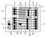
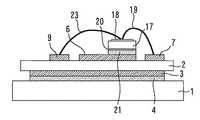
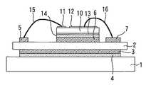
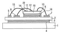
図1は実施の形態1に係る電力用半導体装置を示す平面図である。図2は図1のA−A´に沿った断面図である。図3は図1のB−B´に沿った断面図である。
FIG. 1 is a plan view showing a power semiconductor device according to the first embodiment. FIG. 2 is a cross-sectional view taken along the line AA ′ of FIG. FIG. 3 is a sectional view taken along the line BB ′ of FIG.
放熱板1上に絶縁基板2が設けられている。絶縁基板2の下面に下面電極パターン3が設けられ、この下面電極パターン3は半田4により放熱板1に接合されている。放熱板1はCuなどの熱伝導性の高い材質からなり、絶縁基板2はセラミックなどの絶縁体からなる。半田4は放熱を助ける役割もする。 An
絶縁基板2上に、ゲート電極パターン5、コレクタ電極パターン6、エミッタ電極パターン7(電極パターン)、放熱用パターン8,9が設けられている。これらのパターンはCuなどの電気伝導性及び熱伝導性の高い材質からなる。 On the
絶縁基板2上にIGBTチップ10(電力用半導体素子)が実装されている。IGBTチップ10は、上面にゲート電極11及びエミッタ電極12(主電極)を有し、下面にコレクタ電極13を有する。コレクタ電極13は半田14によりコレクタ電極パターン6に接合されている。ゲート電極11は金属ワイヤ15によりゲート電極パターン5に電気的に接続されている。エミッタ電極12は、金属ワイヤ16(電気的接続部材)によりエミッタ電極パターン7に電気的に接続されている。なお、ワイヤボンディングには超音波接合などが用いられる。 An IGBT chip 10 (power semiconductor element) is mounted on the
絶縁基板2上にダイオードチップ17(電力用半導体素子)が実装されている。ダイオードチップ17の上面のアノード電極18(主電極)は、金属ワイヤ19(電気的接続部材)によりエミッタ電極12に電気的に接続されている。ダイオードチップ17の下面のカソード電極20は、半田21によりコレクタ電極パターン6に接合されている。 A diode chip 17 (power semiconductor element) is mounted on the
エミッタ電極12は、金属ワイヤ22(熱的接続部材)により放熱用パターン8に熱的に接続されている。ダイオードチップ17のアノード電極18は、金属ワイヤ23(熱的接続部材)により放熱用パターン9に熱的に接続されている。実施の形態1では、金属ワイヤ16と金属ワイヤ22は一続きの金属ワイヤであり、金属ワイヤ19と金属ワイヤ23は一続きの金属ワイヤである。 The
エミッタ電極パターン7は装置外部に接続され、エミッタ電極パターン7及び金属ワイヤ16,19に通電される。一方、放熱用パターン8,9は装置外部に接続されず、放熱用パターン8,9及び金属ワイヤ22,23には通電されない。 The
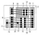
実施の形態1の効果について比較例と比較しながら説明する。図4は比較例に係る電力用半導体装置を示す平面図であり、図5はその断面図である。比較例では、実施の形態1に比べて、放熱用パターン8,9及び金属ワイヤ22,23が存在しない。 The effects of the first embodiment will be described in comparison with a comparative example. 4 is a plan view showing a power semiconductor device according to a comparative example, and FIG. 5 is a sectional view thereof. In the comparative example, the
図6は、ワイヤ接合部の温度振幅とワイヤ接合部の破壊寿命サイクル数の関係図である。実施の形態1では、比較例に比べてワイヤ接合部温度振幅が小さいため、破壊寿命サイクル数が多くなる。これについて以下に説明する。 FIG. 6 is a relationship diagram between the temperature amplitude of the wire joint and the number of fracture life cycles of the wire joint. In
比較例では、IGBTチップ10及びダイオードチップ17の動作時に発生した熱の多くは、素子下面から放熱される。一方、実施の形態1では、放熱用パターン8,9及び金属ワイヤ22,23には通電されず、これら自体が発熱することもない。従って、放熱用パターン8,9及び金属ワイヤ22,23により、素子下面からだけでなく、素子上面からも放熱される。よって、ワイヤ接合部の寿命を向上させることができる。 In the comparative example, most of the heat generated during the operation of the
なお、上記の金属ワイヤは、Al、Cu、又はAuなどの電気伝導性及び熱伝導性の高い金属からなる。また、IGBTチップ10の代わりに、パワーMOSFETチップなどの他の電力用半導体素子を用いてもよい。 In addition, said metal wire consists of a metal with high electrical conductivity and heat conductivity, such as Al, Cu, or Au. Further, instead of the
実施の形態2.
図7は実施の形態2に係る電力用半導体装置を示す平面図であり、図8はその断面図である。実施の形態1では金属ワイヤ16と金属ワイヤ22は一続きの金属ワイヤであったが、実施の形態2ではそれぞれ別の金属ワイヤである。同様に金属ワイヤ19と金属ワイヤ23もそれぞれ別の金属ワイヤである。この場合でも実施の形態1と同様の効果を得ることができる。なお、金属ワイヤ22,23は、断面が短形状のリボンでもよい。
FIG. 7 is a plan view showing a power semiconductor device according to the second embodiment, and FIG. 8 is a sectional view thereof. In the first embodiment, the
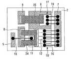
実施の形態3.
図9は実施の形態3に係る電力用半導体装置を示す平面図であり、図10はその断面図である。実施の形態3では、実施の形態1,2の金属ワイヤ22,23の代わりに、放熱用リード端子24,25(熱的接続部材)を用いる。放熱用リード端子24,25は、Al、Cu、又はAuなどの熱伝導性の良い材質からなる。放熱用リード端子24の一端がエミッタ電極12に半田26により接続され、放熱用リード端子24の他端が放熱用パターン8に半田27により接続されている。放熱用リード端子25も同様である。これにより実施の形態1,2よりも放熱性が高くなる。
FIG. 9 is a plan view showing a power semiconductor device according to the third embodiment, and FIG. 10 is a sectional view thereof. In the third embodiment, instead of the
実施の形態4.
図11は実施の形態4に係る電力用半導体装置を示す平面図であり、図12はその断面図である。実施の形態4では、放熱用リード端子24がエミッタ電極12の全面に接続されている。そして、金属ワイヤ16の一端が放熱用リード端子24に接合され、金属ワイヤ16の他端がエミッタ電極パターン7に接合されている。放熱用リード端子25及び金属ワイヤ19も同様である。その他の構成は実施の形態3と同様である。これにより、実施の形態3と同様の効果を得ることができる。
FIG. 11 is a plan view showing a power semiconductor device according to the fourth embodiment, and FIG. 12 is a sectional view thereof. In the fourth embodiment, the heat
2 絶縁基板
7 エミッタ電極パターン(電極パターン)
8,9 放熱用パターン
10 IGBTチップ(電力用半導体素子)
12 エミッタ電極(主電極)
16,19 金属ワイヤ(電気的接続部材)
17 ダイオードチップ(電力用半導体素子)
18 アノード電極(主電極)
22,23 金属ワイヤ(熱的接続部材)
24,25 放熱用リード端子(熱的接続部材)
26 半田2 Insulating
8,9
12 Emitter electrode (main electrode)
16, 19 Metal wire (electrical connection member)
17 Diode chip (Power semiconductor device)
18 Anode electrode (main electrode)
22, 23 Metal wire (thermal connection member)
24, 25 Lead terminal for heat dissipation (thermal connection member)
26 Solder
Claims (5)
Translated fromJapanese前記絶縁基板上に実装され、上面に主電極を有する電力用半導体素子と、
前記絶縁基板上に設けられた電極パターン及び放熱用パターンと、
前記主電極を前記電極パターンに電気的に接続する電気的接続部材と、
前記主電極を前記放熱用パターンに熱的に接続する熱的接続部材とを備え、
前記電極パターンは装置外部に接続され、
前記電極パターン及び前記電気的接続部材に通電され、
前記放熱用パターンは装置外部に接続されず、
前記放熱用パターン及び前記熱的接続部材には通電されないことを特徴とする電力用半導体装置。An insulating substrate;
A power semiconductor element mounted on the insulating substrate and having a main electrode on an upper surface;
An electrode pattern and a heat dissipation pattern provided on the insulating substrate;
An electrical connection member for electrically connecting the main electrode to the electrode pattern;
A thermal connection member that thermally connects the main electrode to the heat dissipation pattern;
The electrode pattern is connected to the outside of the device,
The electrode pattern and the electrical connection member are energized,
The heat dissipation pattern is not connected to the outside of the device,
The power semiconductor device is characterized in that the heat radiation pattern and the thermal connection member are not energized.
前記放熱用リード端子の一端が前記主電極に半田により接続され、
前記放熱用リード端子の他端が前記放熱用パターンに半田により接続されていることを特徴とする請求項1に記載の電力用半導体装置。The thermal connection member is a heat dissipation lead terminal,
One end of the heat dissipation lead terminal is connected to the main electrode by solder,
The power semiconductor device according to claim 1, wherein the other end of the heat dissipation lead terminal is connected to the heat dissipation pattern by solder.
前記金属ワイヤの一端は前記放熱用リード端子に接合され、
前記金属ワイヤの他端は前記電極パターンに接合されていることを特徴とする請求項4に記載の電力用半導体装置。The electrical connection member is a metal wire;
One end of the metal wire is joined to the heat dissipation lead terminal,
The power semiconductor device according to claim 4, wherein the other end of the metal wire is bonded to the electrode pattern.
Priority Applications (1)
| Application Number | Priority Date | Filing Date | Title |
|---|---|---|---|
| JP2010089585AJP2011222707A (en) | 2010-04-08 | 2010-04-08 | Power semiconductor device |
Applications Claiming Priority (1)
| Application Number | Priority Date | Filing Date | Title |
|---|---|---|---|
| JP2010089585AJP2011222707A (en) | 2010-04-08 | 2010-04-08 | Power semiconductor device |
Publications (1)
| Publication Number | Publication Date |
|---|---|
| JP2011222707Atrue JP2011222707A (en) | 2011-11-04 |
Family
ID=45039312
Family Applications (1)
| Application Number | Title | Priority Date | Filing Date |
|---|---|---|---|
| JP2010089585APendingJP2011222707A (en) | 2010-04-08 | 2010-04-08 | Power semiconductor device |
Country Status (1)
| Country | Link |
|---|---|
| JP (1) | JP2011222707A (en) |
Cited By (2)
| Publication number | Priority date | Publication date | Assignee | Title |
|---|---|---|---|---|
| WO2014091608A1 (en)* | 2012-12-13 | 2014-06-19 | 株式会社 日立製作所 | Power semiconductor module and power conversion apparatus using same |
| WO2023140050A1 (en)* | 2022-01-20 | 2023-07-27 | ローム株式会社 | Semiconductor device |
- 2010
- 2010-04-08JPJP2010089585Apatent/JP2011222707A/enactivePending
Cited By (3)
| Publication number | Priority date | Publication date | Assignee | Title |
|---|---|---|---|---|
| WO2014091608A1 (en)* | 2012-12-13 | 2014-06-19 | 株式会社 日立製作所 | Power semiconductor module and power conversion apparatus using same |
| JPWO2014091608A1 (en)* | 2012-12-13 | 2017-01-05 | 株式会社日立製作所 | Power semiconductor module and power converter using the same |
| WO2023140050A1 (en)* | 2022-01-20 | 2023-07-27 | ローム株式会社 | Semiconductor device |
Similar Documents
| Publication | Publication Date | Title |
|---|---|---|
| JP6120704B2 (en) | Semiconductor device | |
| JP6361821B2 (en) | Semiconductor device | |
| JP5863602B2 (en) | Power semiconductor device | |
| JP2013069782A (en) | Semiconductor device | |
| JP2013219267A (en) | Power module | |
| JP6192561B2 (en) | Power semiconductor device | |
| CN115274465A (en) | Power semiconductor devices | |
| JP6448418B2 (en) | Power semiconductor device | |
| KR101734712B1 (en) | Power module | |
| CN104126225A (en) | Semiconductor device | |
| JP2005116702A (en) | Power semiconductor module | |
| JP6684996B2 (en) | Semiconductor device | |
| JP2015090965A (en) | Semiconductor device | |
| JP6598740B2 (en) | Semiconductor device | |
| JP2004221381A (en) | Semiconductor device | |
| EP2178117A1 (en) | Power semiconductor module with double side cooling | |
| JP2011222707A (en) | Power semiconductor device | |
| JP2011176087A (en) | Semiconductor module, and power conversion apparatus | |
| JP5840102B2 (en) | Power semiconductor device | |
| WO2018029801A1 (en) | Semiconductor device | |
| JP2017135144A (en) | Semiconductor module | |
| JP2017199830A (en) | Power module | |
| JP2005310844A (en) | Power semiconductor module | |
| JP4797492B2 (en) | Semiconductor device | |
| JP5682511B2 (en) | Semiconductor module |