JP2011222323A - Metal substrate, carbon nanotube electrode and method for manufacturing the same - Google Patents
Metal substrate, carbon nanotube electrode and method for manufacturing the sameDownload PDFInfo
- Publication number
- JP2011222323A JP2011222323AJP2010090797AJP2010090797AJP2011222323AJP 2011222323 AJP2011222323 AJP 2011222323AJP 2010090797 AJP2010090797 AJP 2010090797AJP 2010090797 AJP2010090797 AJP 2010090797AJP 2011222323 AJP2011222323 AJP 2011222323A
- Authority
- JP
- Japan
- Prior art keywords
- metal substrate
- substrate
- carbon nanotube
- hydrogen
- metal
- Prior art date
- Legal status (The legal status is an assumption and is not a legal conclusion. Google has not performed a legal analysis and makes no representation as to the accuracy of the status listed.)
- Granted
Links
Images


Classifications
- Y—GENERAL TAGGING OF NEW TECHNOLOGICAL DEVELOPMENTS; GENERAL TAGGING OF CROSS-SECTIONAL TECHNOLOGIES SPANNING OVER SEVERAL SECTIONS OF THE IPC; TECHNICAL SUBJECTS COVERED BY FORMER USPC CROSS-REFERENCE ART COLLECTIONS [XRACs] AND DIGESTS
- Y02—TECHNOLOGIES OR APPLICATIONS FOR MITIGATION OR ADAPTATION AGAINST CLIMATE CHANGE
- Y02E—REDUCTION OF GREENHOUSE GAS [GHG] EMISSIONS, RELATED TO ENERGY GENERATION, TRANSMISSION OR DISTRIBUTION
- Y02E10/00—Energy generation through renewable energy sources
- Y02E10/50—Photovoltaic [PV] energy
- Y—GENERAL TAGGING OF NEW TECHNOLOGICAL DEVELOPMENTS; GENERAL TAGGING OF CROSS-SECTIONAL TECHNOLOGIES SPANNING OVER SEVERAL SECTIONS OF THE IPC; TECHNICAL SUBJECTS COVERED BY FORMER USPC CROSS-REFERENCE ART COLLECTIONS [XRACs] AND DIGESTS
- Y02—TECHNOLOGIES OR APPLICATIONS FOR MITIGATION OR ADAPTATION AGAINST CLIMATE CHANGE
- Y02E—REDUCTION OF GREENHOUSE GAS [GHG] EMISSIONS, RELATED TO ENERGY GENERATION, TRANSMISSION OR DISTRIBUTION
- Y02E60/00—Enabling technologies; Technologies with a potential or indirect contribution to GHG emissions mitigation
- Y02E60/10—Energy storage using batteries
- Y—GENERAL TAGGING OF NEW TECHNOLOGICAL DEVELOPMENTS; GENERAL TAGGING OF CROSS-SECTIONAL TECHNOLOGIES SPANNING OVER SEVERAL SECTIONS OF THE IPC; TECHNICAL SUBJECTS COVERED BY FORMER USPC CROSS-REFERENCE ART COLLECTIONS [XRACs] AND DIGESTS
- Y02—TECHNOLOGIES OR APPLICATIONS FOR MITIGATION OR ADAPTATION AGAINST CLIMATE CHANGE
- Y02E—REDUCTION OF GREENHOUSE GAS [GHG] EMISSIONS, RELATED TO ENERGY GENERATION, TRANSMISSION OR DISTRIBUTION
- Y02E60/00—Enabling technologies; Technologies with a potential or indirect contribution to GHG emissions mitigation
- Y02E60/30—Hydrogen technology
- Y02E60/50—Fuel cells
Landscapes
- Photovoltaic Devices (AREA)
- Cell Electrode Carriers And Collectors (AREA)
- Inert Electrodes (AREA)
- Hybrid Cells (AREA)
- Battery Electrode And Active Subsutance (AREA)
- Carbon And Carbon Compounds (AREA)
- Electric Double-Layer Capacitors Or The Like (AREA)
Abstract
Description
Translated fromJapanese本発明は、カーボンナノチューブの形成に好適な金属基板、該金属基板を用いたカーボンナノチューブ電極及びその製造方法に関する。 The present invention relates to a metal substrate suitable for forming carbon nanotubes, a carbon nanotube electrode using the metal substrate, and a method for producing the same.
カーボンナノチューブの製造においてCVD法が通常用いられる。そしてこのCVDのプロセスでは、900〜600度の高温にした炭化水素ガスや水素ガスなどの雰囲気で、基板に担特させた触媒からカーボンナノチューブを成長させている。これまでにカーボンナノチューブを直接成長させた金属基板を電極として、電気二重層キャパシタ(例えば特許文献1参照)や色素増感太陽電池(例えば特許文献2参照)に応用されている。 A CVD method is usually used in the production of carbon nanotubes. In this CVD process, carbon nanotubes are grown from a catalyst dedicated to the substrate in an atmosphere such as hydrocarbon gas or hydrogen gas at a high temperature of 900 to 600 degrees. So far, it has been applied to electric double layer capacitors (for example, see Patent Document 1) and dye-sensitized solar cells (for example, see Patent Document 2) using a metal substrate on which carbon nanotubes are directly grown as an electrode.
このような用途においては、エネルギー密度や可撓性の必要性から一般的に基板を50μm以下に薄くする必要があるため、CVDの高温条件では、使用する水素ガスやプロセス中に炭化水素ガスが分解して発生した水素ガスによって金属基板が脆化する問題が顕著となる。特に、色素増感太陽電池では電解液にヨウ素を用いるため、耐食性の観点から使用される基板の材質はチタンに限定されるが、チタンは非常に安定な水素化物を作るため水素脆化によって薄いチタン基板は可撓性を失い、最悪の場合損壊してしまう。 In such applications, it is generally necessary to thin the substrate to 50 μm or less due to the need for energy density and flexibility. Therefore, under the high temperature conditions of CVD, hydrogen gas used or hydrocarbon gas is generated during the process. The problem that the metal substrate becomes brittle by the hydrogen gas generated by decomposition becomes significant. In particular, in dye-sensitized solar cells, since iodine is used as the electrolyte, the substrate material used from the viewpoint of corrosion resistance is limited to titanium, but titanium is extremely thin due to hydrogen embrittlement to form a very stable hydride. The titanium substrate loses flexibility and is damaged in the worst case.
ところが、特許文献1、および特許文献2を含め従来のカーボンナノチューブ電極の開発においては、基板の脆化を抑制するための技術は開示されていない。チタンの水素脆化を軽減するためには以下のような技術が開示されているが、チタン薄板を電極の基板として用いるには問題解決となっていない。 However, in the development of conventional carbon nanotube electrodes including
(1)まずチタンに酸化膜をつける方法では、室温における水素脆化を防ぐことができても、CVDプロセスの高温条件では水素能化を防ぐことはできなかった。さらに酸化膜をつけることは基板の導電性を損なうので電極としての用途に適していない。
(2)また、浸炭後に真空中の熱処理によって水素を放出させる方法では、浸炭によってカーボンナノチューブの触媒が失活する問題や、触媒からアモルファスカーボンが析出してしまう問題があるため適用できない。(1) In the method of attaching an oxide film to titanium, even though hydrogen embrittlement at room temperature can be prevented, hydrogen activation cannot be prevented under the high temperature conditions of the CVD process. Further, the addition of an oxide film is not suitable for use as an electrode because it impairs the conductivity of the substrate.
(2) Moreover, the method of releasing hydrogen by heat treatment in a vacuum after carburizing is not applicable because there are problems that the carbon nanotube catalyst is deactivated by carburizing and amorphous carbon is precipitated from the catalyst.
(3)また、基板表面の傷や平坦性を向上させ、炭化物、窒化物、炭窒化物を減らして水素吸収を減らす方法では、炭化水素ガスを用いたCVDプロセスを用いるだめ、炭化物の発生は避けられず適用できない。
(4)また、チタンを合金化して水素吸収を軽減化する方法では、合金化はチタンの導電性を損なうので電極としての用途に適していない。
(5)表層にTiC、TiN、Si、SiC、SiN、B、BC、BN、AlNのような被膜を物理気相合成法により形成するする方法では、上記のような材料は導電性に乏しいので電極としての用途に適していない。(3) Further, in the method of improving the scratches and flatness of the substrate surface and reducing the absorption of hydrogen by reducing carbides, nitrides, and carbonitrides, a CVD process using a hydrocarbon gas can be used. Inevitable and not applicable.
(4) In the method of alloying titanium to reduce hydrogen absorption, alloying is not suitable for use as an electrode because the conductivity of titanium is impaired.
(5) In the method of forming a film such as TiC, TiN, Si, SiC, SiN, B, BC, BN, and AlN on the surface layer by physical vapor synthesis, the above materials are poor in conductivity. Not suitable for use as an electrode.
本発明は、このような従来の実情に鑑みて考案されたものであり、導電性を低下させることなく、CVDプロセスにおける水素ガス雰囲気によって引き起こされる水素脆化を軽減または防止した金属基板を提供することを第一の目的とする。
また、本発明は、導電性を低下させることなく、CVDプロセスにおける水素ガス雰囲気によって引き起こされる金属基板の水素脆化を軽減または防止し、基板の可撓性の低下や損壊のないカーボンナノチューブ電極を提供することを第二の目的とする。
また、本発明は、導電性を低下させることなく、CVDプロセスにおける水素ガス雰囲気によって引き起こされる金属基板の水素脆化を軽減または防止し、基板の可撓性の低下や損壊のないカーボンナノチューブ電極を製造することができるカーボンナノチューブ電極の製造方法を提供することを第三の目的とする。The present invention has been devised in view of such a conventional situation, and provides a metal substrate that reduces or prevents hydrogen embrittlement caused by a hydrogen gas atmosphere in a CVD process without lowering conductivity. This is the primary purpose.
In addition, the present invention reduces or prevents hydrogen embrittlement of a metal substrate caused by a hydrogen gas atmosphere in a CVD process without lowering conductivity, and provides a carbon nanotube electrode that does not deteriorate or damage the flexibility of the substrate. The second purpose is to provide it.
In addition, the present invention reduces or prevents hydrogen embrittlement of a metal substrate caused by a hydrogen gas atmosphere in a CVD process without lowering conductivity, and provides a carbon nanotube electrode that does not deteriorate or damage the flexibility of the substrate. A third object is to provide a method for producing a carbon nanotube electrode that can be produced.
本発明の請求項1に記載の金属基板は、金属からなる基体と、前記基体の少なくとも一面側に配された、水素の溶解熱が正である金属材料からなる被膜と、を有することを特徴とする。
本発明の請求項2に記載の金属基板は、請求項1において、前記基体はチタンからなり、その厚さが1〜100μmであることを特徴とする。
本発明の請求項3に記載の金属基板は、請求項1において、前記基体の少なくとも前記一面側又は他面側に配され、鉄、コバルト、ニッケルのうち少なくとも一つを含む金属材料からなる触媒層を有することを特徴とする。
本発明の請求項4に記載のカーボンナノチューブ電極は、請求項1乃至3のいずれかに記載の金属基板上に、カーボンナノチューブを成長させてなることを特徴とする。
本発明の請求項5に記載のカーボンナノチューブの製造方法は、請求項1乃至3のいずれかに記載の金属基板を用い、該金属基板上に炭素を含むガスを作用させることにより前記金属基板上にカーボンナノチューブを成長させる工程を少なくとも備えたことを特徴とする。The metal substrate according to
The metal substrate according to
A metal substrate according to a third aspect of the present invention is the catalyst according to the first aspect, wherein the catalyst is made of at least one of iron, cobalt, and nickel, and is disposed on at least one side or the other side of the substrate. It has a layer.
A carbon nanotube electrode according to a fourth aspect of the present invention is characterized in that carbon nanotubes are grown on the metal substrate according to any one of the first to third aspects.
According to a fifth aspect of the present invention, there is provided a method for producing a carbon nanotube, comprising: using the metal substrate according to any one of the first to third aspects; and causing a gas containing carbon to act on the metal substrate. And at least a step of growing carbon nanotubes.
本発明の金属基板は、少なくとも一面側に、水素の溶解熱が正である金属材料からなる被膜を有しているので、該金属基板をCVDプロセスに用いた場合に、導電性を低下させることなく、水素ガス雰囲気によって引き起こされる基体の水素脆化を軽減または防止することができる。
本発明のカーボンナノチューブ電極は、少なくとも一面側に、水素の溶解熱が正である金属材料からなる被膜を有する金属基板を用いているので、導電性を低下させることなく、CVDプロセスにおける水素ガス雰囲気によって引き起こされる金属基板の水素脆化を軽減または防止することができる。その結果、本発明では基板の可撓性の低下や損壊のないカーボンナノチューブ電極を提供することができる。
本発明のカーボンナノチューブ電極の製造方法では、少なくとも一面側に、水素の溶解熱が正である金属材料からなる被膜を有する金属基板を用いているので、CVDプロセスを用いてカーボンナノチューブを成長させる場合に、導電性を低下させることなく、水素ガス雰囲気によって引き起こされる金属基板の水素脆化を軽減または防止することができる。その結果、本発明では基板の可撓性の低下や損壊のないカーボンナノチューブ電極を製造することができる。Since the metal substrate of the present invention has a coating made of a metal material having a positive hydrogen heat of dissolution on at least one side, the conductivity is lowered when the metal substrate is used in a CVD process. In addition, hydrogen embrittlement of the substrate caused by the hydrogen gas atmosphere can be reduced or prevented.
The carbon nanotube electrode of the present invention uses a metal substrate having a coating made of a metal material having a positive hydrogen heat of dissolution on at least one side, so that the hydrogen gas atmosphere in the CVD process can be obtained without reducing the conductivity. It is possible to reduce or prevent hydrogen embrittlement of the metal substrate caused by. As a result, the present invention can provide a carbon nanotube electrode that does not cause a decrease in flexibility or damage to the substrate.
In the method for producing a carbon nanotube electrode of the present invention, when a metal substrate having a coating made of a metal material having a positive heat of hydrogen dissolution is used on at least one side, carbon nanotubes are grown using a CVD process. In addition, hydrogen embrittlement of the metal substrate caused by the hydrogen gas atmosphere can be reduced or prevented without reducing the conductivity. As a result, in the present invention, it is possible to produce a carbon nanotube electrode that does not cause a decrease in flexibility or damage to the substrate.
以下、本発明の金属基板、カーボンナノチューブ電極及びその製造方法の好適な形態について説明する。 Hereinafter, preferred embodiments of the metal substrate, the carbon nanotube electrode, and the manufacturing method thereof according to the present invention will be described.
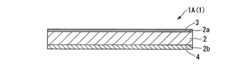
図1は、本発明の金属基板の一例を模式的に示す断面図である。
本発明の金属基板1A(1)は、金属からなる基体2と、前記基体2の少なくとも一面2a側に配された、水素の溶解熱が正である金属材料からなる被膜3と、を有することを特徴とする。
本発明の金属基板1A(1)は、少なくとも一面2a側に、水素の溶解熱が正である金属材料からなる被膜3を有しているので、該金属基板1をCVDプロセスに用いた場合に、導電性を低下させることなく、水素ガス雰囲気によって引き起こされる基体2の水素脆化を軽減または防止することができる。FIG. 1 is a cross-sectional view schematically showing an example of a metal substrate of the present invention.
The
Since the
基体2としては、特に限定されるものではないが、は、例えばチタン、ジルコニウム、バナジウム、ニオブ等からなるが、チタンからなることが好ましい。また、基体2の厚さは、例えば1〜100μmである。 Although it does not specifically limit as the base |
被膜3は、水素の溶解熱が正で、水素化物を作りにくい金属材料からなる。
このような金属材料としては、例えばアルミニウム、鋼、金、銀、白金、イリジウム、ロジウム、ルテニウム、タングステン、モリブデンなどが挙げられる。これらの金属は、水素の溶解熱が正のため水素の浸入が遅く、基体2への水素への浸入が抑えられる。
なお、水素の溶解熱が正である金属材料としては、上述したものの他にマグネシウム、鉄、ニッケル、コバルトなども挙げられるが、マグネシウムは水素化物を作りやすいために、他の水素の溶解熱が正の金属被膜と比べ水素脆化の抑制効果が低い。また、鉄、ニッケル、コバルトは炭化物を作りやすく、アモルファスカーボンを析出しやすいために被膜3として適さない。The
Examples of such a metal material include aluminum, steel, gold, silver, platinum, iridium, rhodium, ruthenium, tungsten, and molybdenum. Since these metals have positive heat of dissolution of hydrogen, the penetration of hydrogen is slow and the penetration of hydrogen into the
In addition to the above-described metal materials, the metal material having positive heat of dissolution of hydrogen includes magnesium, iron, nickel, cobalt, etc. However, since magnesium easily forms hydride, the heat of dissolution of other hydrogen is also known. The effect of suppressing hydrogen embrittlement is lower than that of a positive metal film. Further, iron, nickel, and cobalt are not suitable as the
このように、水素脆化しやすい基体2上に、水素の溶解熱が正で、水素化物を作りにくい金属材料からなる被膜3をつけることによって、電極基板としての導電性を損なうことなく基体2の水素脆化を軽減、または防ぐことができる。また、本発明によれば、従来の被膜をつける水素脆化軽減の方法に比べて、被膜3が金属なので導電性が高く、電極基板としての特性を損なわない。
また、前記被膜3の厚さとしては、特に限定されるものではないが、例えば10〜1000[nm]であることが好ましい。As described above, by applying the
The thickness of the
また、この金属基板1A(1)上にカーボンナノチューブ5を成長させる場合、金属基板1A(1)は、前記基体2の少なくとも前記一面2a側又は他面2b側に配された触媒層4を有する。触媒層4の材料としては、例えば鉄、コバルト、ニッケルをのうち少なくとも一つを含むものが用いられる。
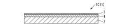
なお、図1では、被膜3と触媒層4とが基体2の異なる面にそれぞれ配された場合を例として示しているが、これに限定されるものではなく、被膜3と触媒層4とが基体2の同じ面側に配されていてもよい。この場合、図2に示すように、基体2の一面2a上に被膜3が配され、該被膜3上に触媒層4が配されていてもよいし、図3に示すように、基体2の一面2a上に触媒層4が配され、該触媒層4上に被膜3が配されていてもよい。また、被膜3は基体2の両面に配されていてもよい。When the
FIG. 1 shows an example in which the
次に、上述したような金属基板1を用いたカーボンナノチューブ電極について説明する。
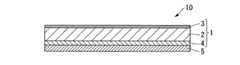
図4は、本発明のカーボンナノチューブ電極10の一構成例を示す断面図である。
本発明のカーボンナノチューブ電極10は、前記金属基板1の触媒層4上に、カーボンナノチューブ5を成長させてなることを特徴とする。Next, a carbon nanotube electrode using the
FIG. 4 is a cross-sectional view showing a configuration example of the carbon nanotube electrode 10 of the present invention.
The carbon nanotube electrode 10 of the present invention is characterized in that
本発明のカーボンナノチューブ電極10は、少なくとも一面側に、水素の溶解熱が正である金属材料からなる被膜3を有する金属基板1を用いているので、導電性を低下させることなく、CVDプロセスにおける水素ガス雰囲気によって引き起こされる基体2の水素脆化を軽減または防止することができる。その結果、本発明では基板の可撓性の低下や損壊のないカーボンナノチューブ電極10を提供することができる。
このようなカーボンナノチューブ電極10は、色素増感太陽電池、リチウムイオン二次電池、リチウムイオンキャパシタ、電気二重層キャパシタ、及び燃料電池などの電極として好適に用いることができる。Since the carbon nanotube electrode 10 of the present invention uses the
Such a carbon nanotube electrode 10 can be suitably used as an electrode for a dye-sensitized solar cell, a lithium ion secondary battery, a lithium ion capacitor, an electric double layer capacitor, and a fuel cell.
また、本発明のカーボンナノチューブの製造方法は、前記金属基板1を用い、該金属基板1上に炭素を含むガスを作用させることにより、金属基板1上にカーボンナノチューブ5を成長させる工程を少なくとも備えたことを特徴とする。
具体的には、後述するような製造装置20を用いて、真空処理室21の内部空間に炭素含有のプロセスガスを導入し、該プロセスガスにマイクロ波を照射して生起させたプラズマから、支持体23に載置された基板30(非処理体)の表面にカーボンナノチューブ5を気相成長させる。このとき本発明では、前記基板30(非処理体)として前記金属基板1を用いる。Further, the carbon nanotube production method of the present invention includes at least a step of growing the
Specifically, using a manufacturing apparatus 20 as will be described later, a carbon-containing process gas is introduced into the internal space of the
本発明のカーボンナノチューブ電極の製造方法では、少なくとも一面側に、水素の溶解熱が正である金属材料からなる被膜3を有する金属基板1を用いているので、CVDプロセスを用いてカーボンナノチューブ5を成長させる場合に、導電性を低下させることなく、水素ガス雰囲気によって引き起こされる基体2の水素脆化を軽減または防止することができる。その結果、本発明では基板の可撓性の低下や損壊のないカーボンナノチューブ電極10を製造することができる。 In the method of manufacturing a carbon nanotube electrode according to the present invention, the
図5は、カーボンナノチューブの製造装置の一構成例を示す模式的断面図である。
このカーボンナノチューブの製造装置20は、平板状のマイクロ波導入部22を備え、内部空間に炭素含有のプロセスガスを導入しながら所定の圧力状態を維持する真空処理室21と、前記内部空間にあって、前記マイクロ波導入部22に対向配置されるように、基板30(平板状の被処理体)を載置する支持体23と、前記支持体23に内蔵された温度制御手段24と、を少なくとも備える。
カーボンナノチューブの製造装置20は、マイクロ波プラズマを利用して、基板(非処理体)表面にカーボンナノチューブを気相成長させる装置である。FIG. 5 is a schematic cross-sectional view showing a configuration example of a carbon nanotube production apparatus.
The carbon nanotube production apparatus 20 includes a flat plate-like
The carbon nanotube manufacturing apparatus 20 is an apparatus for vapor-phase growing carbon nanotubes on the surface of a substrate (non-processed body) using microwave plasma.
真空処理室21は、平板状のマイクロ波導入部22を備え、内部空間に炭素含有のプロセスガスを導入しながら所定の圧力状態を維持する。
真空処理室21には、プロセスガスを導入するガス導入手段25と、このプロセスガスを導入しながら所定の圧力状態を維持するための真空排気手段26がそれぞれ接続されている。ガス導入手段25は、ガス管を介して図示しないガス源に連通している。The
Connected to the
カーボンナノチューブを金属基板1の表面に気相成長させる際に導入する炭素含有のプロセスガスとしては、メタン、アセチレンなどの炭化水素ガス若しくは気化させたアルコール、または気相成長における希釈と触媒作用のために、これらのガスに水素、アンモニア、窒素若しくはアルゴンのうち少なくとも1つを混合したものが用いられる。好ましくは、メタンなど、加熱した基板温度で分解しないものを用いる。 The carbon-containing process gas introduced when the carbon nanotubes are vapor-grown on the surface of the
この真空処理室21に、大口径のプラズマを生成するために、基本モードで伝播する小径導波管から、高次モードが複数存在し得る大口径の導波管へ拡大するテーパ型のマイクロ波導入部22が接続されている。このマイクロ波導入部22と真空処理室21とは、マイクロ波導入窓27により空間的に仕切られている。 In order to generate a large-diameter plasma in the
支持体23は、前記真空処理室21の内部空間にあって、前記マイクロ波導入部22に対向配置されるように、平板状の被処理体を載置する。
特に、本発明では、基板30(非処理体)として前記金属基板1を用いる。上述したように水素の溶解熱が正で、水素化物を作りにくい金属材料からなる被膜を有する金属基板1を用いることによって、電極基板としての導電性を損なうことなく基体2の水素脆化を軽減、または防ぐことができる。また、本発明によれば、従来の被膜をつける水素脆化軽減の方法に比べて、被膜3が金属なので導電性が高く、電極基板としての特性を損なわない。The
In particular, in the present invention, the
前記支持体23には、基板30を所定の温度範囲に保つ温度制御手段24(例えばヒーター)が内蔵されている。
温度制御手段24によって基板30を加熱することで、カーボンナノチューブを気相成長させる際に、基板温度の制御が容易になり、また、低温でカーボンナノチューブを気相成長させることが可能になる。前記基板30が500〜850[℃]の範囲内の所定温度に保持されるように、温度制御手段24の作動を制御することが好ましい。The
When the
このような製造装置20を用いて、真空処理室21の内部空間に炭素含有のプロセスガスを導入し、該プロセスガスにマイクロ波を照射して生起させたプラズマから、支持体23に載置された基板30(非処理体)の表面にカーボンナノチューブを気相成長させる。
このようにして得られたカーボンナノチューブ電極10は、少なくとも一面側に、水素の溶解熱が正である金属材料からなる被膜3を有する金属基板1を用いているので、CVDプロセスにおける水素ガス雰囲気によって引き起こされる基体2の水素脆化を軽減または防止することができる。その結果、得られるカーボンナノチューブ電極10は、基板の可撓性の低下や損壊のないものとなる。Using such a manufacturing apparatus 20, a carbon-containing process gas is introduced into the internal space of the
Since the carbon nanotube electrode 10 thus obtained uses the
図5に示したような製造装置を用いて、金属基板上にカーボンナノチューブを成長させた。
(実施例1)
チタン基板(厚さ3、10、20、40、100μm)の一方の面に、触媒層としてニッケル薄膜を形成した。また、チタン基板の他方の面に厚さ50nmのアルミニウム被膜を形成し、金属基板を作製した。
このようにして得られた金属基板を、マイクロ波プラズマCVD装置のヒーターが内蔵されたステージ(支持体)上に置いた。出力300Wで基板の直上にプラズマを発生させ、CVDにより金属基板上にカーボンナノチューブを成長させた。Carbon nanotubes were grown on a metal substrate using a manufacturing apparatus as shown in FIG.
Example 1
A nickel thin film was formed as a catalyst layer on one surface of a titanium substrate (
The metal substrate thus obtained was placed on a stage (support) in which a heater of a microwave plasma CVD apparatus was incorporated. Plasma was generated immediately above the substrate at an output of 300 W, and carbon nanotubes were grown on the metal substrate by CVD.
(実施例2)
アルミニウム被膜の厚さを100nmとしたこと以外は、実施例1と同様にして金属基板を作製し、この金属基板上にカーボンナノチューブを成長させた。
(実施例3)
チタン基板の一方の面に、触媒層としてニッケル薄膜を形成した。また、触媒層上に厚さ5nmのアルミニウム被膜を形成して金属基板を作製し、この金属基板上にカーボンナノチューブを成長させた。(Example 2)
A metal substrate was prepared in the same manner as in Example 1 except that the thickness of the aluminum coating was 100 nm, and carbon nanotubes were grown on this metal substrate.
(Example 3)
A nickel thin film was formed as a catalyst layer on one surface of the titanium substrate. In addition, a 5 nm thick aluminum film was formed on the catalyst layer to produce a metal substrate, and carbon nanotubes were grown on this metal substrate.
(実施例4)
アルミニウム被膜の厚さを10nmとしたこと以外は、実施例1と同様にして金属基板を作製し、この金属基板上にカーボンナノチューブを成長させた。Example 4
A metal substrate was produced in the same manner as in Example 1 except that the thickness of the aluminum coating was 10 nm, and carbon nanotubes were grown on this metal substrate.
(比較例1)
アルミニウム被膜を形成しなったこと以外は、実施例1と同様にして金属基板を作製し、この金属基板上にカーボンナノチューブを成長させた。
(比較例2)
アルミニウム被膜の代わりに、チタンの酸化被膜を形成したこと以外は、実施例1と同様にして金属基板を作製し、この金属基板1上にカーボンナノチューブを成長させた。(Comparative Example 1)
A metal substrate was produced in the same manner as in Example 1 except that the aluminum coating was not formed, and carbon nanotubes were grown on the metal substrate.
(Comparative Example 2)
A metal substrate was produced in the same manner as in Example 1 except that a titanium oxide film was formed instead of the aluminum film, and carbon nanotubes were grown on the
実施例1〜実施例4で得られたカーボンナノチューブ電極では、基板の水素脆化が少なく、基板の導電性も良好であった。
これに対し、比較例1、比較例2のカーボンナノチューブ電極では、板の水素脆化が大きく、割れてしまった。
また、実施例1で作製したカーボンナノチューブ電極を対極に用いて、色素増殖太陽電池を作製したところ、良好な特性を示した。In the carbon nanotube electrodes obtained in Examples 1 to 4, there was little hydrogen embrittlement of the substrate, and the conductivity of the substrate was also good.
On the other hand, in the carbon nanotube electrodes of Comparative Example 1 and Comparative Example 2, the hydrogen embrittlement of the plate was large and cracked.
Moreover, when the carbon nanotube electrode produced in Example 1 was used for a counter electrode and the pigment | dye proliferation solar cell was produced, the favorable characteristic was shown.
以上、本発明の金属基板、カーボンナノチューブ電極及びその製造方法について説明してきたが、本発明は上述した例に限定されるものではなく、発明の趣旨を逸脱しない範囲で適宜変更可能である。 As mentioned above, although the metal substrate of this invention, the carbon nanotube electrode, and its manufacturing method were demonstrated, this invention is not limited to the example mentioned above, In the range which does not deviate from the meaning of invention, it can change suitably.
本発明は、金属基板、カーボンナノチューブ電極及びその製造方法に広く適用可能である。 The present invention is widely applicable to metal substrates, carbon nanotube electrodes, and methods for manufacturing the same.
1A、1B,1C(1) 金属基板、2 基体、3 被膜、4 触媒層、5 カーボンナノチューブ、10 カーボンナノチューブ電極。 1A, 1B, 1C (1) Metal substrate, 2 substrate, 3 coating, 4 catalyst layer, 5 carbon nanotube, 10 carbon nanotube electrode.
Claims (5)
Translated fromJapanese前記金属基板上に炭素を含むガスを作用させることにより前記金属基板上にカーボンナノチューブを成長させる工程を少なくとも備えたことを特徴とするカーボンナノチューブ電極の製造方法。Using the metal substrate according to any one of claims 1 to 3,
A method for producing a carbon nanotube electrode, comprising at least a step of growing carbon nanotubes on the metal substrate by causing a gas containing carbon to act on the metal substrate.
Priority Applications (1)
| Application Number | Priority Date | Filing Date | Title |
|---|---|---|---|
| JP2010090797AJP5746830B2 (en) | 2010-04-09 | 2010-04-09 | Metal substrate, carbon nanotube electrode and manufacturing method thereof |
Applications Claiming Priority (1)
| Application Number | Priority Date | Filing Date | Title |
|---|---|---|---|
| JP2010090797AJP5746830B2 (en) | 2010-04-09 | 2010-04-09 | Metal substrate, carbon nanotube electrode and manufacturing method thereof |
Publications (2)
| Publication Number | Publication Date |
|---|---|
| JP2011222323Atrue JP2011222323A (en) | 2011-11-04 |
| JP5746830B2 JP5746830B2 (en) | 2015-07-08 |
Family
ID=45039054
Family Applications (1)
| Application Number | Title | Priority Date | Filing Date |
|---|---|---|---|
| JP2010090797AExpired - Fee RelatedJP5746830B2 (en) | 2010-04-09 | 2010-04-09 | Metal substrate, carbon nanotube electrode and manufacturing method thereof |
Country Status (1)
| Country | Link |
|---|---|
| JP (1) | JP5746830B2 (en) |
Cited By (17)
| Publication number | Priority date | Publication date | Assignee | Title |
|---|---|---|---|---|
| JP2012151052A (en)* | 2011-01-20 | 2012-08-09 | Fujikura Ltd | Structure for carbon nanotube electrode, carbon nanotube electrode, and dye sensitized solar cell |
| CN114388275A (en)* | 2022-01-20 | 2022-04-22 | 重庆大学 | A kind of TiC nanotube array material and its preparation method and application |
| US11590568B2 (en) | 2019-12-19 | 2023-02-28 | 6K Inc. | Process for producing spheroidized powder from feedstock materials |
| US11633785B2 (en) | 2019-04-30 | 2023-04-25 | 6K Inc. | Mechanically alloyed powder feedstock |
| US11717886B2 (en) | 2019-11-18 | 2023-08-08 | 6K Inc. | Unique feedstocks for spherical powders and methods of manufacturing |
| US11839919B2 (en) | 2015-12-16 | 2023-12-12 | 6K Inc. | Spheroidal dehydrogenated metals and metal alloy particles |
| US11855278B2 (en) | 2020-06-25 | 2023-12-26 | 6K, Inc. | Microcomposite alloy structure |
| US11919071B2 (en) | 2020-10-30 | 2024-03-05 | 6K Inc. | Systems and methods for synthesis of spheroidized metal powders |
| US11963287B2 (en) | 2020-09-24 | 2024-04-16 | 6K Inc. | Systems, devices, and methods for starting plasma |
| US12040162B2 (en) | 2022-06-09 | 2024-07-16 | 6K Inc. | Plasma apparatus and methods for processing feed material utilizing an upstream swirl module and composite gas flows |
| US12042861B2 (en) | 2021-03-31 | 2024-07-23 | 6K Inc. | Systems and methods for additive manufacturing of metal nitride ceramics |
| US12094688B2 (en) | 2022-08-25 | 2024-09-17 | 6K Inc. | Plasma apparatus and methods for processing feed material utilizing a powder ingress preventor (PIP) |
| US12195338B2 (en) | 2022-12-15 | 2025-01-14 | 6K Inc. | Systems, methods, and device for pyrolysis of methane in a microwave plasma for hydrogen and structured carbon powder production |
| US12214420B2 (en) | 2015-12-16 | 2025-02-04 | 6K Inc. | Spheroidal titanium metallic powders with custom microstructures |
| US12261023B2 (en) | 2022-05-23 | 2025-03-25 | 6K Inc. | Microwave plasma apparatus and methods for processing materials using an interior liner |
| US12311447B2 (en) | 2018-06-19 | 2025-05-27 | 6K Inc. | Process for producing spheroidized powder from feedstock materials |
| US12406829B2 (en) | 2021-01-11 | 2025-09-02 | 6K Inc. | Methods and systems for reclamation of Li-ion cathode materials using microwave plasma processing |
Citations (9)
| Publication number | Priority date | Publication date | Assignee | Title |
|---|---|---|---|---|
| JP2004284919A (en)* | 2003-03-25 | 2004-10-14 | Mitsubishi Electric Corp | Method for manufacturing substrate for forming carbon nanotube and method for manufacturing carbon nanotube using this substrate |
| JP2005145743A (en)* | 2003-11-13 | 2005-06-09 | Kenjiro Oura | Carbon nanotube, its manufacturing method, carbon nanotube device and electrical double layer capacitor |
| JP2006202721A (en)* | 2004-12-22 | 2006-08-03 | Fujikura Ltd | Counter electrode for photoelectric conversion element and photoelectric conversion element |
| JP2007230832A (en)* | 2006-03-02 | 2007-09-13 | Sanyo Electric Co Ltd | Carbon nanotube electrode and manufacturing method thereof |
| JP2007280849A (en)* | 2006-04-10 | 2007-10-25 | Fujikura Ltd | Photoelectric conversion element |
| JP2009173476A (en)* | 2008-01-22 | 2009-08-06 | Panasonic Corp | Carbon nanotube structure, manufacturing method thereof, and energy device using the same |
| WO2009125540A1 (en)* | 2008-04-11 | 2009-10-15 | パナソニック株式会社 | Energy storage device, method for manufacturing same, and apparatus equipped with same |
| WO2010092786A1 (en)* | 2009-02-10 | 2010-08-19 | 日本ゼオン株式会社 | Base for producing oriented carbon nanotube aggregate, and method for producing oriented carbon nanotube aggregate |
| JP2011219343A (en)* | 2010-03-26 | 2011-11-04 | Aisin Seiki Co Ltd | Carbon nanotube composite and method for producing same |
- 2010
- 2010-04-09JPJP2010090797Apatent/JP5746830B2/ennot_activeExpired - Fee Related
Patent Citations (9)
| Publication number | Priority date | Publication date | Assignee | Title |
|---|---|---|---|---|
| JP2004284919A (en)* | 2003-03-25 | 2004-10-14 | Mitsubishi Electric Corp | Method for manufacturing substrate for forming carbon nanotube and method for manufacturing carbon nanotube using this substrate |
| JP2005145743A (en)* | 2003-11-13 | 2005-06-09 | Kenjiro Oura | Carbon nanotube, its manufacturing method, carbon nanotube device and electrical double layer capacitor |
| JP2006202721A (en)* | 2004-12-22 | 2006-08-03 | Fujikura Ltd | Counter electrode for photoelectric conversion element and photoelectric conversion element |
| JP2007230832A (en)* | 2006-03-02 | 2007-09-13 | Sanyo Electric Co Ltd | Carbon nanotube electrode and manufacturing method thereof |
| JP2007280849A (en)* | 2006-04-10 | 2007-10-25 | Fujikura Ltd | Photoelectric conversion element |
| JP2009173476A (en)* | 2008-01-22 | 2009-08-06 | Panasonic Corp | Carbon nanotube structure, manufacturing method thereof, and energy device using the same |
| WO2009125540A1 (en)* | 2008-04-11 | 2009-10-15 | パナソニック株式会社 | Energy storage device, method for manufacturing same, and apparatus equipped with same |
| WO2010092786A1 (en)* | 2009-02-10 | 2010-08-19 | 日本ゼオン株式会社 | Base for producing oriented carbon nanotube aggregate, and method for producing oriented carbon nanotube aggregate |
| JP2011219343A (en)* | 2010-03-26 | 2011-11-04 | Aisin Seiki Co Ltd | Carbon nanotube composite and method for producing same |
Cited By (18)
| Publication number | Priority date | Publication date | Assignee | Title |
|---|---|---|---|---|
| JP2012151052A (en)* | 2011-01-20 | 2012-08-09 | Fujikura Ltd | Structure for carbon nanotube electrode, carbon nanotube electrode, and dye sensitized solar cell |
| US11839919B2 (en) | 2015-12-16 | 2023-12-12 | 6K Inc. | Spheroidal dehydrogenated metals and metal alloy particles |
| US12214420B2 (en) | 2015-12-16 | 2025-02-04 | 6K Inc. | Spheroidal titanium metallic powders with custom microstructures |
| US12311447B2 (en) | 2018-06-19 | 2025-05-27 | 6K Inc. | Process for producing spheroidized powder from feedstock materials |
| US11633785B2 (en) | 2019-04-30 | 2023-04-25 | 6K Inc. | Mechanically alloyed powder feedstock |
| US11717886B2 (en) | 2019-11-18 | 2023-08-08 | 6K Inc. | Unique feedstocks for spherical powders and methods of manufacturing |
| US11590568B2 (en) | 2019-12-19 | 2023-02-28 | 6K Inc. | Process for producing spheroidized powder from feedstock materials |
| US12176529B2 (en) | 2020-06-25 | 2024-12-24 | 6K Inc. | Microcomposite alloy structure |
| US11855278B2 (en) | 2020-06-25 | 2023-12-26 | 6K, Inc. | Microcomposite alloy structure |
| US11963287B2 (en) | 2020-09-24 | 2024-04-16 | 6K Inc. | Systems, devices, and methods for starting plasma |
| US11919071B2 (en) | 2020-10-30 | 2024-03-05 | 6K Inc. | Systems and methods for synthesis of spheroidized metal powders |
| US12406829B2 (en) | 2021-01-11 | 2025-09-02 | 6K Inc. | Methods and systems for reclamation of Li-ion cathode materials using microwave plasma processing |
| US12042861B2 (en) | 2021-03-31 | 2024-07-23 | 6K Inc. | Systems and methods for additive manufacturing of metal nitride ceramics |
| CN114388275A (en)* | 2022-01-20 | 2022-04-22 | 重庆大学 | A kind of TiC nanotube array material and its preparation method and application |
| US12261023B2 (en) | 2022-05-23 | 2025-03-25 | 6K Inc. | Microwave plasma apparatus and methods for processing materials using an interior liner |
| US12040162B2 (en) | 2022-06-09 | 2024-07-16 | 6K Inc. | Plasma apparatus and methods for processing feed material utilizing an upstream swirl module and composite gas flows |
| US12094688B2 (en) | 2022-08-25 | 2024-09-17 | 6K Inc. | Plasma apparatus and methods for processing feed material utilizing a powder ingress preventor (PIP) |
| US12195338B2 (en) | 2022-12-15 | 2025-01-14 | 6K Inc. | Systems, methods, and device for pyrolysis of methane in a microwave plasma for hydrogen and structured carbon powder production |
Also Published As
| Publication number | Publication date |
|---|---|
| JP5746830B2 (en) | 2015-07-08 |
Similar Documents
| Publication | Publication Date | Title |
|---|---|---|
| JP5746830B2 (en) | Metal substrate, carbon nanotube electrode and manufacturing method thereof | |
| Liu et al. | Advances of microwave plasma-enhanced chemical vapor deposition in fabrication of carbon nanotubes: a review | |
| US11673807B2 (en) | Carbon nanostructured materials and methods for forming carbon nanostructured materials | |
| JP3819382B2 (en) | Carbon nanotube matrix and growth method thereof | |
| JP3837451B2 (en) | Method for producing carbon nanotube | |
| Zhang et al. | Electronic transport and corrosion mechanisms of graphite-like nanocrystalline carbon films used on metallic bipolar plates in proton-exchange membrane fuel cells | |
| US20190003042A1 (en) | Graphene synthesis | |
| CN107058971A (en) | The preparation method and application of graphene composite material | |
| JP2013166692A (en) | Method for producing substrate with conductive diamond film formed thereon | |
| JP2009078956A (en) | Carbon nanotube composite, energy device using the same, and method for producing carbon nanotube composite | |
| Tian et al. | Synthesis of AAB‐stacked single‐crystal graphene/hBN/graphene trilayer van der waals heterostructures by in situ CVD | |
| CN101570329B (en) | Method for preparing carbon nanofiber | |
| Yousefi et al. | Possible high efficiency platform for biosensors based on optimum physical chemistry of carbon nanotubes | |
| CN102976313A (en) | Preparation method for graphene | |
| Kudinova et al. | A magnetron sputtering method for the application of the Ni catalyst for the synthesis process of carbon nanotube arrays | |
| KR20210055903A (en) | Method for forming bi-layer graphene | |
| JP6972627B2 (en) | Method for manufacturing carbon nanotube composite and laminated body | |
| JP2006306704A (en) | Method of forming carbon film and carbon film | |
| JP5653822B2 (en) | Method for producing carbon nanotube | |
| JP6210445B2 (en) | Method for producing carbon nanotube | |
| Kumar et al. | Unveiling active sites by structural tailoring of two‐dimensional niobium disulfide for improved electrocatalytic hydrogen evolution reaction | |
| Acharya et al. | Water assisted atmospheric CVD super growth of vertically aligned CNT forest for supercapacitor application | |
| JP7163645B2 (en) | Carbon nanotube electrode, electricity storage device using the same, and method for producing carbon nanotube composite | |
| Kishimoto et al. | Growth of mm-long carbon nanotubes by grid-inserted plasma-enhanced chemical vapor deposition | |
| Mills et al. | Improvement in the Electrical Properties of Nickel‐Plated Steel Using Graphitic Carbon Coatings |
Legal Events
| Date | Code | Title | Description |
|---|---|---|---|
| A621 | Written request for application examination | Free format text:JAPANESE INTERMEDIATE CODE: A621 Effective date:20121206 | |
| A977 | Report on retrieval | Free format text:JAPANESE INTERMEDIATE CODE: A971007 Effective date:20140227 | |
| A131 | Notification of reasons for refusal | Free format text:JAPANESE INTERMEDIATE CODE: A131 Effective date:20140304 | |
| A521 | Request for written amendment filed | Free format text:JAPANESE INTERMEDIATE CODE: A523 Effective date:20140507 | |
| A131 | Notification of reasons for refusal | Free format text:JAPANESE INTERMEDIATE CODE: A131 Effective date:20140902 | |
| A521 | Request for written amendment filed | Free format text:JAPANESE INTERMEDIATE CODE: A523 Effective date:20141029 | |
| TRDD | Decision of grant or rejection written | ||
| A01 | Written decision to grant a patent or to grant a registration (utility model) | Free format text:JAPANESE INTERMEDIATE CODE: A01 Effective date:20150414 | |
| A61 | First payment of annual fees (during grant procedure) | Free format text:JAPANESE INTERMEDIATE CODE: A61 Effective date:20150511 | |
| R151 | Written notification of patent or utility model registration | Ref document number:5746830 Country of ref document:JP Free format text:JAPANESE INTERMEDIATE CODE: R151 | |
| R250 | Receipt of annual fees | Free format text:JAPANESE INTERMEDIATE CODE: R250 | |
| R250 | Receipt of annual fees | Free format text:JAPANESE INTERMEDIATE CODE: R250 | |
| R250 | Receipt of annual fees | Free format text:JAPANESE INTERMEDIATE CODE: R250 | |
| R250 | Receipt of annual fees | Free format text:JAPANESE INTERMEDIATE CODE: R250 | |
| R250 | Receipt of annual fees | Free format text:JAPANESE INTERMEDIATE CODE: R250 | |
| LAPS | Cancellation because of no payment of annual fees |