JP2011205207A - Communication terminal - Google Patents
Communication terminalDownload PDFInfo
- Publication number
- JP2011205207A JP2011205207AJP2010068109AJP2010068109AJP2011205207AJP 2011205207 AJP2011205207 AJP 2011205207AJP 2010068109 AJP2010068109 AJP 2010068109AJP 2010068109 AJP2010068109 AJP 2010068109AJP 2011205207 AJP2011205207 AJP 2011205207A
- Authority
- JP
- Japan
- Prior art keywords
- housing
- circuit board
- transparent conductive
- casing
- conductive sheet
- Prior art date
- Legal status (The legal status is an assumption and is not a legal conclusion. Google has not performed a legal analysis and makes no representation as to the accuracy of the status listed.)
- Pending
Links
Images


Landscapes
- Support Of Aerials (AREA)
- Telephone Set Structure (AREA)
Abstract
Translated fromJapaneseDescription
Translated fromJapanese本発明は、通信端末装置に関し、特に開閉自在な複数の筐体を有する通信端末装置に関する。 The present invention relates to a communication terminal device, and more particularly to a communication terminal device having a plurality of cases that can be opened and closed.
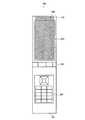
従来、2つの筐体が開閉可能に連結されて構成された無線装置が知られている。図1は、開閉可能な無線装置1の閉じた状態の側面図である。図1に示すように、無線装置1は、下筐体10と、上筐体11と、ヒンジ部12と、回路基板13と、回路基板14と、アンテナ素子15とを有する。無線装置1は、下筐体10と上筐体11とが重なり合う閉じた状態において、アンテナ素子15に給電した際に、回路基板13と回路基板14とのグランド電流が流れる。この際、回路基板13を流れるグランド電流e1と、回路基板14を流れるグランド電流e2とは、互いに打ち消し合う方向に流れる。従って、無線装置1は、待ち受け等の閉じた状態において、アンテナ性能の劣化が生じるという課題がある。 2. Description of the Related Art Conventionally, a wireless device configured by connecting two housings so as to be opened and closed is known. FIG. 1 is a side view of a wireless device 1 that can be opened and closed in a closed state. As illustrated in FIG. 1, the wireless device 1 includes a
この課題を解決する方法として、特許文献1に示す無線装置が知られている。特許文献1によれば、閉じた状態において下筐体に相対する上筐体の面上に、上接地領域と接続された上短絡部を設け、上筐体に相対する下筐体の面上で上短絡部と接触する位置に、下接地領域と接続された下短絡部を設ける。これにより、閉じた状態におけるアンテナ性能の劣化を低減することができる。 As a method for solving this problem, a wireless device disclosed in Patent Document 1 is known. According to Patent Document 1, an upper short-circuit portion connected to the upper grounding region is provided on the surface of the upper housing that faces the lower housing in the closed state, and the surface of the lower housing that faces the upper housing. A lower short-circuit portion connected to the lower grounding region is provided at a position where the upper short-circuit portion comes into contact. Thereby, degradation of the antenna performance in the closed state can be reduced.
しかしながら、特許文献1においては、上短絡部と下短絡部とを物理的に接続する必要があるので、上短絡部と下短絡部との接続不良によりアンテナ性能が劣化するという問題がある。また、特許文献1においては、上短絡部と下短絡部との位置合わせを精度良く行う必要があるので、製造工程が複雑になり、製造コストが増大するという問題がある。 However, in Patent Document 1, since it is necessary to physically connect the upper short-circuit portion and the lower short-circuit portion, there is a problem that the antenna performance deteriorates due to poor connection between the upper short-circuit portion and the lower short-circuit portion. Moreover, in patent document 1, since it is necessary to perform alignment with an upper short circuit part and a lower short circuit part with a sufficient precision, a manufacturing process becomes complicated and there exists a problem that manufacturing cost increases.
本発明の目的は、アンテナ性能の劣化を確実に低減することができるとともに、製造容易にして製造コストの増大を抑制することができる通信端末装置を提供することである。 An object of the present invention is to provide a communication terminal device that can surely reduce deterioration of antenna performance and can be easily manufactured to suppress an increase in manufacturing cost.
本発明の通信端末装置は、第1の筐体と、前記第1の筐体に対して回転自在に前記第1の筐体と接続する第2の筐体と、前記第1の筐体に設けられる第1の回路基板と、前記第2の筐体に設けられる第2の回路基板と、前記第1の回路基板に設けられる無線回路と、前記第1の筐体に設けられ、前記無線回路と電気的に接続するアンテナ素子と、前記第1の筐体または前記第2の筐体に設けられ、前記第1の筐体と前記第2の筐体とが上下に重なり合う閉じた状態において前記第1の回路基板と前記第2の回路基板との間に配置される導電部材と、を具備する構成を採る。 The communication terminal device according to the present invention includes a first casing, a second casing that is connected to the first casing so as to be rotatable with respect to the first casing, and the first casing. A first circuit board provided; a second circuit board provided in the second casing; a wireless circuit provided in the first circuit board; and a wireless circuit provided in the first casing. An antenna element that is electrically connected to a circuit, provided in the first casing or the second casing, and in a closed state in which the first casing and the second casing overlap each other vertically A conductive member disposed between the first circuit board and the second circuit board is employed.
本発明によれば、アンテナ性能の劣化を確実に低減することができるとともに、製造容易にして製造コストの増大を抑制することができる。 According to the present invention, it is possible to reliably reduce the deterioration of the antenna performance, facilitate manufacturing, and suppress an increase in manufacturing cost.
以下、本発明の実施の形態について、図面を参照して詳細に説明する。 Hereinafter, embodiments of the present invention will be described in detail with reference to the drawings.
(実施の形態)
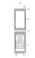
図2は、本発明の実施の形態に係る通信端末装置100の閉じた状態の側面図である。(Embodiment)
FIG. 2 is a side view of the
通信端末装置100は、第1の筐体101と、第2の筐体102と、ヒンジ部103と、回路基板104と、回路基板105と、無線回路106と、アンテナ素子107とから主に構成される。以下に、各構成について、詳細に説明する。 The
第1の筐体101は、ヒンジ部103を介して、第2の筐体102に対して回転自在に第2の筐体102と接続する。また、第1の筐体101は、閉じた状態において、図2に示すように、第2の筐体102と上下に重なり合う。また、第1の筐体101は、回路基板104と、無線回路106と、アンテナ素子107と、透明導電性シート108とを有する。 The
第2の筐体102は、ヒンジ部103を介して、第1の筐体101に対して図2のX方向に回転自在に第1の筐体101と接続する。これにより、通信端末装置100は、図2の閉じた状態と、閉じた状態から第2の筐体102が図2のX1方向に回転した図示しない開いた状態とになる。また、第2の筐体102は、回路基板105を有する。また、閉じた状態において第1の筐体101に対向する第2の筐体102の表面には、透明導電性シート108が貼着されている。 The
ヒンジ部103は、第1の筐体101と第2の筐体102とを、閉じた状態と開いた状態との間で、X方向に互いに回転自在に接続する。また、ヒンジ部103は、近傍にアンテナ素子107が設けられる。 The
回路基板104は、第1の筐体101の内部の略全面に設けられる。また、回路基板104は、無線回路106が設けられる。また、回路基板104は、アンテナ素子107のグランド電流が流れる導電部を有する。また、回路基板104は、図示しない回路パターンが印刷形成される。また、回路基板104は、閉じた状態において、透明導電性シート108と容量結合することにより、透明導電性シート108を介して回路基板105と電気的に接続する。また、回路基板104は、ヒンジ部103中に存在する図示しないフレキシブルプリント基板等を介して回路基板105と電気的に接続する。 The
回路基板105は、第2の筐体102の内部の略全面に設けられる。また、回路基板105は、アンテナ素子107のグランド電流が流れる導電部を有する。また、回路基板105は、図示しない回路パターンが印刷形成される。また、回路基板105は、閉じた状態において、透明導電性シート108と容量結合する。 The
無線回路106は、回路基板104のヒンジ部103側に設けられ、所定の無線処理を行う。また、無線回路106は、アンテナ素子107と電気的に接続する。 The
アンテナ素子107は、第1の筐体101のヒンジ部103の近傍に設けられる。また、アンテナ素子107は、無線回路106と電気的に接続される。また、アンテナ素子107は、所定の周波数で共振する。 The
透明導電性シート108は、シート状であり、透明な材料により形成される。また、透明導電性シート108は、閉じた状態において、回路基板104と回路基板105との間に位置する。また、透明導電性シート108は、閉じた状態において、第1の筐体101と対向する第2の筐体102の外表面部に貼着される。また、透明導電性シート108は、閉じた状態において、回路基板104と容量結合する。なお、透明導電性シート108の詳細については、後述する。 The transparent
上記の構成を有する通信端末装置100によれば、回路基板104と回路基板105とが透明導電性シート108を介して容量結合することにより、回路基板104と回路基板105との電磁結合を強くすることができる。これにより、回路基板104と回路基板105の双方において、アンテナ電流e10が同一方向(図2の右方向)に流れる。以上で、通信端末装置100の構成の説明を終える。 According to the
次に、透明導電性シート108について、詳細に説明する。 Next, the transparent
図3は、透明導電性シート108を貼着した通信端末装置100の開いた状態の平面図である。なお、図3において、透明導電性シート108を斜線で示す。 FIG. 3 is a plan view of the
図3において、第1の筐体101は、操作パネル部301を有する。また、第2の筐体102は、表示部302を有する。また、透明導電性シート108は、第2の筐体102に設けられる。また、この際、透明導電性シート108は、閉じた状態において、第1の筐体101と対向する第2の筐体102の外表面部の、表示部302を含む略全面に貼着される。 In FIG. 3, the
図4は、本実施の形態の第1の変形例の透明導電性シート108を貼着した通信端末装置100の開いた状態の平面図である。なお、図4において、透明導電性シート108を斜線で示す。 FIG. 4 is a plan view of the
図4において、第1の筐体101は、操作パネル部401を有する。また、第2の筐体102は、表示部402を有する。また、透明導電性シート108は、第1の筐体101に設けられる。また、この際、透明導電性シート108は、閉じた状態において、第2の筐体102と対向する第1の筐体101の外表面部の、操作パネル部401を含む略全面に貼着される。 In FIG. 4, the
図5は、本実施の形態の第2の変形例の透明導電性シート108a、108bを貼着した通信端末装置100の開いた状態の平面図である。なお、図5において、透明導電性シート108を斜線で示す。 FIG. 5 is a plan view of the
図5において、第1の筐体101は、操作パネル部501を有する。また、第2の筐体102は、表示部502を有する。また、透明導電性シート108aは、第1の筐体101に設けられる。また、この際、透明導電性シート108aは、閉じた状態において、第2の筐体102と対向する第1の筐体101の外表面部の、下端に貼着される。また、透明導電性シート108bは、第2の筐体102に設けられる。また、この際、透明導電性シート108bは、閉じた状態において、第1の筐体101と対向する第2の筐体102の外表面部の、上端に貼着される。 In FIG. 5, the
図6は、本実施の形態の第3の変形例の透明導電性シート108c、108d、108eを貼着した通信端末装置100の開いた状態の平面図である。なお、図6において、透明導電性シート108を斜線で示す。 FIG. 6 is a plan view of the
図6において、第1の筐体101は、操作パネル部601を有する。また、第2の筐体102は、表示部602を有する。また、透明導電性シート108cは、第1の筐体101に設けられる。また、この際、透明導電性シート108cは、閉じた状態において、第2の筐体102と対向する第1の筐体101の外表面部の、下端に貼着される。また、透明導電性シート108dは、第1の筐体101に設けられる。また、この際、透明導電性シート108dは、閉じた状態において、第2の筐体102と対向する第1の筐体101の外表面部の、上端に貼着される。また、透明導電性シート108eは、第2の筐体102に設けられる。また、この際、透明導電性シート108eは、閉じた状態において、第1の筐体101と対向する第2の筐体102の外表面部の、上端に貼着される。 In FIG. 6, the
図7は、本実施の形態の第4の変形例の透明導電性シート108f、108gを貼着した通信端末装置100の開いた状態の平面図である。なお、図7において、透明導電性シート108を斜線で示す。 FIG. 7 is a plan view of the
図7において、第1の筐体101は、操作パネル部701を有する。また、第2の筐体102は、表示部702を有する。また、透明導電性シート108fは、第1の筐体101に設けられる。また、この際、透明導電性シート108fは、閉じた状態において、第2の筐体102と対向する第1の筐体101の外表面部の、操作パネル部701の周囲に環状に貼着される。また、透明導電性シート108gは、第2の筐体102に設けられる。また、この際、透明導電性シート108gは、閉じた状態において、第1の筐体101と対向する第2の筐体102の外表面部の、表示部702の周囲に環状に貼着される。 In FIG. 7, the
このように、本実施の形態によれば、閉じた状態において上下に重なり合う筐体の回路基板間を透明導電性シートにより容量結合するので、各回路基板のグランド電流を同一方向に流すことができる。この結果、アンテナ性能の劣化を確実に低減することができる。また、本実施の形態によれば、閉じた状態において、各筐体の回路基板間に透明導電性シートを配置するだけでよいので、正確な位置合わせを不要にすることができ、製造容易にして製造コストの増大を抑制することができる。また、本実施の形態によれば、透明導電性シートを用いたので、表示部または操作パネル部と緩衝する位置に設けることができるとともに、外表面部に貼り付けるので、製造容易にして製造コストの増大を抑制することができる。また、本実施の形態によれば、透明導電性シートを用いたので、通信端末装置の外表面部に貼着した場合でも、通信端末装置の外観上のデザイン性を損なうことを防ぐことができる。また、本実施の形態によれば、透明導電性シートと各回路基板とを容量結合したので、接続不良等によるアンテナ性能の劣化を防ぐことができる。また、本実施の形態によれば、シート状の導電部材を用いて回路基板間を電気的に接続したので、通信端末装置を薄型化することができる。また、本実施の形態によれば、透明導電性シートを筐体の表面の上端または下端に設けた場合には、透明導電性シートの大きさを小さくできるので、製造コストに占める透明導電性シートの費用を低減でき、製造コストを低減することができる。 As described above, according to the present embodiment, the circuit boards of the casings that overlap vertically in the closed state are capacitively coupled by the transparent conductive sheet, so that the ground current of each circuit board can flow in the same direction. . As a result, it is possible to reliably reduce the deterioration of the antenna performance. Further, according to the present embodiment, in the closed state, it is only necessary to arrange the transparent conductive sheet between the circuit boards of the respective housings. Thus, an increase in manufacturing cost can be suppressed. Further, according to the present embodiment, since the transparent conductive sheet is used, it can be provided at a position where it can be buffered with the display unit or the operation panel unit, and can be attached to the outer surface part, so that it can be manufactured easily and manufactured at a low cost. Can be suppressed. Moreover, according to this Embodiment, since the transparent conductive sheet was used, even if it sticks to the outer surface part of a communication terminal device, it can prevent impairing the design property on the external appearance of a communication terminal device. . Further, according to the present embodiment, since the transparent conductive sheet and each circuit board are capacitively coupled, it is possible to prevent deterioration of antenna performance due to poor connection or the like. Moreover, according to this Embodiment, since the circuit boards were electrically connected using the sheet-like conductive member, the communication terminal device can be thinned. In addition, according to the present embodiment, when the transparent conductive sheet is provided at the upper end or the lower end of the surface of the housing, the size of the transparent conductive sheet can be reduced, so that the transparent conductive sheet occupies the manufacturing cost. The manufacturing cost can be reduced.
なお、上記の実施の形態において、二つ折り形式の通信端末装置に適用したが、本発明はこれに限らず、スライド式等の任意の開閉自在な通信端末装置に適用することができる。また、上記の実施の形態において、透明導電性シートにより回路基板間を容量結合することとしたが、閉じた状態において回路基板間に位置する筐体の一部を、導電性を有する透明部材により形成し、導電性を有する筐体により回路基板間を容量結合することとしてもよい。また、上記の実施の形態において、ヒンジ部の近傍にアンテナ素子を配置したが、本発明はこれに限らず、筐体のヒンジ部を設けた端部と反対側の端部にアンテナ素子を設けてもよい。また、上記の実施の形態において、無線回路106を回路基板104のヒンジ部側に設けることとしたが、本発明はこれに限らず、無線回路106を回路基板104のヒンジ部側以外のところに設けることとしてもよく、回路基板105に設けることとしてもよい。また、上記の実施の形態において、閉じた状態において下側の第1の筐体にアンテナ素子を設けたが、閉じた状態において上側の第2の筐体にアンテナ素子を設けてもよい。また、上記の実施の形態において、透明導電性シートにより回路基板間を容量結合することとしたが、本発明はこれに限らず、透明でない導電性シートにより回路基板間を容量結合することとしてもよい。また、上記の実施の形態において、透明導電性シートを筐体の外表面部に貼着したが、本発明はこれに限らず、透明導電性シートを筐体の内部に設けてもよい。また、回路基板104を第1の筐体101の内部の略全面に設けることとしたが、本発明はこれに限らず、回路基板104を第1の筐体101の内部の一部に設けることとしてもよい。また、回路基板105を第2の筐体102の内部の略全面に設けることとしたが、本発明はこれに限らず、回路基板105を第2の筐体102の内部の一部に設けることとしてもよい。 In the above-described embodiment, the present invention is applied to a two-fold type communication terminal device. However, the present invention is not limited to this, and can be applied to any open / closed communication terminal device such as a slide type. Further, in the above embodiment, the circuit boards are capacitively coupled by the transparent conductive sheet. However, a part of the housing located between the circuit boards in the closed state is made by the conductive transparent member. Alternatively, the circuit boards may be capacitively coupled with each other by a conductive casing. In the above embodiment, the antenna element is arranged in the vicinity of the hinge part. However, the present invention is not limited to this, and the antenna element is provided at the end opposite to the end provided with the hinge part of the housing. May be. In the above embodiment, the
本発明は、特に開閉自在な複数の筐体を有する通信端末装置に好適である。 The present invention is particularly suitable for a communication terminal apparatus having a plurality of cases that can be opened and closed.
100 通信端末装置
101 第1の筐体
102 第2の筐体
103 ヒンジ部
104、105 回路基板
106 無線回路
107 アンテナ素子
108 透明導電性シート
e10 グランド電流DESCRIPTION OF
Claims (4)
Translated fromJapanese前記第1の筐体に対して回転自在に前記第1の筐体と接続する第2の筐体と、
前記第1の筐体に設けられる第1の回路基板と、
前記第2の筐体に設けられる第2の回路基板と、
前記第1の回路基板に設けられる無線回路と、
前記第1の筐体に設けられ、前記無線回路と電気的に接続するアンテナ素子と、
前記第1の筐体または前記第2の筐体に設けられ、前記第1の筐体と前記第2の筐体とが上下に重なり合う閉じた状態において前記第1の回路基板と前記第2の回路基板との間に配置される導電部材と、
を具備する通信端末装置。A first housing;
A second housing connected to the first housing so as to be rotatable with respect to the first housing;
A first circuit board provided in the first housing;
A second circuit board provided in the second housing;
A radio circuit provided on the first circuit board;
An antenna element provided in the first housing and electrically connected to the radio circuit;
The first circuit board and the second circuit board are provided in the first casing or the second casing, and the first circuit board and the second casing are closed in a state where the first casing and the second casing overlap each other vertically. A conductive member disposed between the circuit board and the circuit board;
A communication terminal device comprising:
Priority Applications (1)
| Application Number | Priority Date | Filing Date | Title |
|---|---|---|---|
| JP2010068109AJP2011205207A (en) | 2010-03-24 | 2010-03-24 | Communication terminal |
Applications Claiming Priority (1)
| Application Number | Priority Date | Filing Date | Title |
|---|---|---|---|
| JP2010068109AJP2011205207A (en) | 2010-03-24 | 2010-03-24 | Communication terminal |
Publications (1)
| Publication Number | Publication Date |
|---|---|
| JP2011205207Atrue JP2011205207A (en) | 2011-10-13 |
Family
ID=44881426
Family Applications (1)
| Application Number | Title | Priority Date | Filing Date |
|---|---|---|---|
| JP2010068109APendingJP2011205207A (en) | 2010-03-24 | 2010-03-24 | Communication terminal |
Country Status (1)
| Country | Link |
|---|---|
| JP (1) | JP2011205207A (en) |
Cited By (1)
| Publication number | Priority date | Publication date | Assignee | Title |
|---|---|---|---|---|
| US11509752B2 (en) | 2017-08-22 | 2022-11-22 | Futurewei Technologies, Inc | Foldable mobile device |
Citations (3)
| Publication number | Priority date | Publication date | Assignee | Title |
|---|---|---|---|---|
| JPH0485836U (en)* | 1990-11-28 | 1992-07-27 | ||
| JPH11122023A (en)* | 1997-10-16 | 1999-04-30 | Ntt Kansai Personal Tsushinmo Kk | Window glass antenna |
| JP2004229141A (en)* | 2003-01-24 | 2004-08-12 | Sharp Corp | Mobile terminal equipment |
- 2010
- 2010-03-24JPJP2010068109Apatent/JP2011205207A/enactivePending
Patent Citations (3)
| Publication number | Priority date | Publication date | Assignee | Title |
|---|---|---|---|---|
| JPH0485836U (en)* | 1990-11-28 | 1992-07-27 | ||
| JPH11122023A (en)* | 1997-10-16 | 1999-04-30 | Ntt Kansai Personal Tsushinmo Kk | Window glass antenna |
| JP2004229141A (en)* | 2003-01-24 | 2004-08-12 | Sharp Corp | Mobile terminal equipment |
Cited By (1)
| Publication number | Priority date | Publication date | Assignee | Title |
|---|---|---|---|---|
| US11509752B2 (en) | 2017-08-22 | 2022-11-22 | Futurewei Technologies, Inc | Foldable mobile device |
Similar Documents
| Publication | Publication Date | Title |
|---|---|---|
| KR102031203B1 (en) | Antenna laminate and image display device including the same | |
| EP2664073B1 (en) | Electronic device with a peripheral conductive member forming part of an antenna resonating element | |
| JP5355897B2 (en) | Portable radio | |
| CN101257526B (en) | Combined battery cap lateral grounding structure of mobile communication terminal | |
| JP4691595B2 (en) | transceiver | |
| JP6323455B2 (en) | Antenna device | |
| JP2008048376A (en) | Antenna coil to be mounted on circuit board and antenna device | |
| CN103633421B (en) | Antenna assembly | |
| JP2008160589A (en) | High impedance substrate, antenna device, and portable radio device | |
| JP2011120071A (en) | Portable radio device | |
| JP4472408B2 (en) | Mobile terminal device | |
| CN105048075A (en) | Antenna device | |
| CN202218474U (en) | Main circuit board of mobile terminal and mobile terminal | |
| WO2006022381A1 (en) | Portable radio | |
| CN104347927B (en) | Antenna and hand-hold communication appliance | |
| US20140085151A1 (en) | Device and communication device including antenna | |
| US20090267843A1 (en) | Antenna modules and portable electronic devices employing the same | |
| KR20170094692A (en) | Flexible printed circuit board | |
| US20100013721A1 (en) | Antenna device and portable radio apparatus using the same | |
| WO2015096690A1 (en) | Fpc of capacitive touch screen and method for mounting fpc | |
| JP2011205207A (en) | Communication terminal | |
| JP2011040884A (en) | Portable wireless device | |
| WO2011067942A1 (en) | Wireless communication terminal | |
| JP2005303543A (en) | Mobile terminal device | |
| KR20160135440A (en) | Antenna integrated Flexible printed circuit board |
Legal Events
| Date | Code | Title | Description |
|---|---|---|---|
| A977 | Report on retrieval | Free format text:JAPANESE INTERMEDIATE CODE: A971007 Effective date:20120523 | |
| A131 | Notification of reasons for refusal | Free format text:JAPANESE INTERMEDIATE CODE: A131 Effective date:20120529 | |
| A02 | Decision of refusal | Free format text:JAPANESE INTERMEDIATE CODE: A02 Effective date:20121002 |