JP2011198486A - Microwave processing device - Google Patents
Microwave processing deviceDownload PDFInfo
- Publication number
- JP2011198486A JP2011198486AJP2010060624AJP2010060624AJP2011198486AJP 2011198486 AJP2011198486 AJP 2011198486AJP 2010060624 AJP2010060624 AJP 2010060624AJP 2010060624 AJP2010060624 AJP 2010060624AJP 2011198486 AJP2011198486 AJP 2011198486A
- Authority
- JP
- Japan
- Prior art keywords
- door
- power
- unit
- door switch
- microwave
- Prior art date
- Legal status (The legal status is an assumption and is not a legal conclusion. Google has not performed a legal analysis and makes no representation as to the accuracy of the status listed.)
- Pending
Links
Images


Landscapes
- Control Of High-Frequency Heating Circuits (AREA)
- Constitution Of High-Frequency Heating (AREA)
Abstract
Translated fromJapaneseDescription
Translated fromJapanese本発明は、半導体素子を用いて構成したマイクロ波発生部を備えたマイクロ波処理装置に関するものである。 The present invention relates to a microwave processing apparatus including a microwave generation unit configured using a semiconductor element.
従来のマイクロ波処理装置は、一般には電子レンジに代表されるようにマイクロ波発生手段にマグネトロンと称される真空管を用いているものが一般的である。 A conventional microwave processing apparatus generally uses a vacuum tube called a magnetron as a microwave generating means as represented by a microwave oven.
近年、このマグネトロンに代えて、窒化ガリウム(GaN)などの半導体素子を用いた高周波加熱装置の開発が進められている。マイクロ波は電子レンジに係わらず誘電加熱を応用する機器に展開可能である(例えば、特許文献1参照)。 In recent years, a high-frequency heating apparatus using a semiconductor element such as gallium nitride (GaN) instead of the magnetron has been developed. Microwaves can be developed in devices that apply dielectric heating regardless of the microwave oven (see, for example, Patent Document 1).
GaNを用いたときの効果としては小型、軽量かつ容易に周波数や位相を可変することができる。一方、従来マグネトロンや、それを付勢する電源に関しては容積が大きく、重量が重いため、マイクロ波を主熱源あるいは補助熱源として利用するアイデアは多く存在するが実用には至っていなかった。特許文献1ではマイクロ波漏洩に対する安全性としての扉体開閉に連動して漏洩電波を停止する安全装置に関する技術を開示している。 As an effect when using GaN, the frequency and phase can be easily varied in a small size and light weight. On the other hand, the conventional magnetron and the power source for energizing the magnetron have a large volume and a heavy weight, so there are many ideas to use the microwave as a main heat source or an auxiliary heat source, but they have not been put into practical use.
しかし、従来技術の構成では、扉体と連動してマイクロ波発生手段への商用電源の供給を停止する安全スイッチを二重に設けることにより、扉体の開放にともなう漏洩電波を阻止し、安全性の担保を図ろうとするものであったが、GaNを用いた固体発振装置の場合ノーマリーON型FET(外部からバイアス電圧が入っていない状態でトラジスタ動作する)を用いることが一般的で、電源供給を一斉遮断してしまうとトランジスタが破壊してしまうという課題があった。 However, in the configuration of the conventional technology, a safety switch that stops the supply of commercial power to the microwave generation means in conjunction with the door body is doubled to prevent leakage radio waves due to the door body opening, In the case of a solid-state oscillation device using GaN, it is common to use a normally-on type FET (transistor operation with no external bias voltage) in the case of a solid-state oscillation device using GaN. If the supply is shut off all at once, there is a problem that the transistor is destroyed.
例えば、ノーマリーONのGaNトラジスタであれば、ドレイン−ソース間に電圧が印加された状態でゲートバイアス電圧を除去してしまうと、トランジスタ内部でショート回路が形成され短絡破壊してしまう。 For example, in the case of a normally-on GaN transistor, if the gate bias voltage is removed while a voltage is applied between the drain and source, a short circuit is formed inside the transistor, causing a short circuit breakdown.
本発明は、上記従来の課題を解決するもので、扉体と連動して電源ラインの開閉を司る二つの機械的接点を有し、かつ、ノーマリーONのトランジスタを有するマイクロ波処理装置においても、トランジスタを破壊しない信頼性が高く安全性に優れたマイクロ波処理装置を提供することを目的とする。 The present invention solves the above-described conventional problems, and has two mechanical contacts that control opening and closing of a power supply line in conjunction with a door body, and also in a microwave processing apparatus having a normally ON transistor, An object of the present invention is to provide a microwave processing apparatus that is highly reliable and safe without destroying a transistor.
上記従来の課題を解決するために、本発明にかかるマイクロ波処理装置は、加熱室と、加熱室に被加熱物を収納自在とし開成時にはマイクロ波の漏洩を阻止するドアと、マイクロ波の基準信号を作成する発振部と、発振部の出力を受け半導体素子を用いた複数段のアンプでかつ少なくとも複数段のアンプの最終段はノーマリーON型のFETを用いた半導体で構成された電力増幅を行うパワーユニットと、パワーユニットから出力されるマイクロ波電力を放射するアンテナと、パワーユニットのドレイン又はコレクタに印加される正極電圧を作成する正極電圧供給部と、エミッタ又はソースに印加され負極電圧を作成する負極電圧供給部と、ベース又はゲートに印加されるバイアス電圧を作成するバイアス電圧供給部とを具備した電源部と、ドアの開閉と連動して開成または閉成する機械的接点を有する第一のドアスイッチと第二のドアスイッチと、電荷を充電して所定の電圧を供給してバイアス電圧供給部を形成する電荷蓄積部と、電荷蓄積部から電圧供給を受けバイアス電圧供給部の電圧を電源部と独立して確立し、商用電源が遮断され電源部への電力供給がなくなって電源部への電力供給がなくなった時でもバイアス電圧を維持し続けトランジスタが破壊することを回避する高い信頼性を有するとともに、第一のドアスイッチと第二のドアスイッチを有することでドア開閉と連動した二重の発振停止装置を有するものである。 In order to solve the above-described conventional problems, a microwave processing apparatus according to the present invention includes a heating chamber, a door that can store an object to be heated in the heating chamber and prevents microwave leakage at the time of opening, and a microwave reference Amplifying unit for creating a signal, and a multi-stage amplifier using a semiconductor element that receives the output of the oscillating unit, and at least the final stage of the multi-stage amplifier performs power amplification composed of a semiconductor using a normally-on type FET. A power unit to perform, an antenna that radiates microwave power output from the power unit, a positive voltage supply that creates a positive voltage applied to the drain or collector of the power unit, and a negative electrode that creates a negative voltage applied to the emitter or source A power supply unit comprising a voltage supply unit and a bias voltage supply unit that creates a bias voltage applied to the base or the gate; A first door switch and a second door switch having a mechanical contact that opens or closes in conjunction with opening and closing of the door, and a charge that charges the charge and supplies a predetermined voltage to form a bias voltage supply unit Establishing the voltage of the bias voltage supply unit independently of the power supply unit, receiving voltage supply from the storage unit and the charge storage unit, shutting off the commercial power supply and eliminating power supply to the power supply unit Double oscillation stop device that has high reliability to maintain the bias voltage even when it is in contact and avoids breakdown of the transistor and interlocks with opening and closing of the door by having the first door switch and the second door switch It is what has.
本発明のマイクロ波処理装置は、ノーマリーON型のトランジスタを用いたパワーユニットを駆動する電源部がドアの開成によって電力供給が絶たれても、静電容量が極めて大きく蓄えられた電荷で電圧を長時間維持する電気的二重層コンデンサを有した電荷蓄積部によってバイアス電圧を独立して維持し、ドアの開成により電源部に商用電源からの電力供給が絶たれても、ノーマリーON型のトランジスタが破壊することはなく高い信頼性を保持するとともに、二重の発振停止装置を有し、ドア開時には使用者にマイクロ波を暴露させないことを確実にした安全性にも優れたマイクロ波処理装置を提供することができる。 The microwave processing apparatus according to the present invention increases the voltage with the charge that is stored in a very large capacitance even when the power supply that drives the power unit using a normally-on transistor is cut off by opening the door. Bias voltage is maintained independently by the charge storage unit with the electric double layer capacitor that maintains the time, and the normally ON type transistor is destroyed even if power supply from the commercial power supply is cut off by opening the door Highly reliable microwave processing equipment that maintains high reliability and has a double oscillation stop device, ensuring that the user is not exposed to microwaves when the door is opened can do.
第1の発明は、被加熱物を収容する加熱室と、加熱室から機外へ電波の漏洩を遮断する開閉自在のドアと、マイクロ波の基準信号を作成する発振部と、発振部の出力を受け半導体素子を用いた複数段のアンプでかつ少なくとも複数段のアンプの最終段はノーマリーON型のFETを用いた半導体で構成された電力増幅を行うパワーユニットと、パワーユニットから出力されるマイクロ波電力を放射するアンテナと、パワーユニットのドレイン又はコレクタに印加される正極電圧を作成する正極電圧供給部と、エミッタ又はソースに印加され負極電圧を作成する負極電圧供給部と、ベース又はゲートに印加されるバイアス電圧を作成するバイアス電圧供給部とを具備した電源部と、ドアの開閉と連動して開成または閉成する機械的接点を有し電源ラインを開閉する第一のドアスイッチと第二のドアスイッチと、前記バイアス電圧供給部を形成し電荷を充電して所定の電圧をパワーユニットに供給する電荷蓄積部とを備えたものである。 According to a first aspect of the present invention, there is provided a heating chamber that accommodates an object to be heated, an openable / closable door that blocks leakage of radio waves from the heating chamber to the outside of the apparatus, an oscillation unit that generates a microwave reference signal, and an output of the oscillation unit The power unit is a multi-stage amplifier using semiconductor elements, and at least the final stage of the multi-stage amplifier is composed of a semiconductor using a normally-on type FET, and a power unit for amplifying power, and microwave power output from the power unit Antenna, a positive voltage supply for creating a positive voltage applied to the drain or collector of the power unit, a negative voltage supply for creating a negative voltage applied to the emitter or source, and applied to the base or gate A power supply unit having a bias voltage supply unit for generating a bias voltage, and a mechanical contact that opens or closes in conjunction with opening and closing of the door. A first door switch and the second door switch for opening and closing the line, and charge the formed charge the bias voltage supply unit is obtained by a charge storage unit to supply to the power unit a predetermined voltage.
本発明によれば、電荷蓄積部には極めて大きな静電容量をもち蓄積された電荷で長時間所望電圧を維持する電気的二重層コンデンサを用い、前記第一のドアスイッチと第二のドアスイッチの閉成により電源部に商用電源を供給する構成とすることにより、第一のドアスイッチもしくは第二のドアスイッチが開成することで、電源部への電力供給が絶たれても、独立して電荷蓄積部がバイアス電圧を維持し、電源部への電力供給が遮断されてもノーマリーON型のFETを破壊することを回避できる。 According to the present invention, the first door switch and the second door switch are used in the charge storage section using an electric double layer capacitor having a very large capacitance and maintaining a desired voltage for a long time with the stored charge. When the first door switch or the second door switch is opened, the power supply to the power supply section is opened independently. Even if the charge storage unit maintains the bias voltage and the power supply to the power supply unit is interrupted, it is possible to avoid destroying the normally-on type FET.
また、第一のドアスイッチと第二のドアスイッチが、ドアと連動して二重に開成するため、ドアが開かれても確実に電源部への電力供給を絶ち発振を停止させるため、使用者へのマイクロ波の暴露は確実に防止することができる。 Also, since the first door switch and the second door switch are double-opened in conjunction with the door, the power supply to the power supply section is cut off and oscillation is stopped without fail even if the door is opened. Exposure to microwaves can be reliably prevented.
第2の発明は、電荷蓄積部の電気的二重層コンデンサを、プリント基板に実装するときに製造工程において端子間から充電することにより、電気的二重層コンデンサへの充電を容易かつ短時間に実行することができる。 In the second invention, the electric double layer capacitor of the charge storage unit is charged from between the terminals in the manufacturing process when mounted on the printed circuit board, so that the electric double layer capacitor can be charged easily and in a short time. can do.
第3の発明は、電荷蓄積部の電気的二重層コンデンサには予め製造前に電荷を充電することにより、プリント基板に電気的二重層コンデンサを実装するだけで満充電を確保することができ、作業性を著しく簡便化することができる。 According to the third aspect of the present invention, the electric double layer capacitor of the charge accumulating portion is charged in advance before manufacturing, so that full charge can be ensured only by mounting the electric double layer capacitor on the printed circuit board. Workability can be remarkably simplified.
(実施の形態)
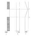
図1は本発明の実施の形態におけるマイクロ波処理装置の概観斜視図である。ドア1は、被加熱物10を収納する。ヒンジ7は、ドア1を支え、ヒンジ取付け穴A8を通して筐体内部に出入り可能となっており、終端は筐体に固定された螺旋バネ(図示していない)に取り付けられており、取付け穴B9を通してドア1に係合されている。(Embodiment)
FIG. 1 is a schematic perspective view of a microwave processing apparatus according to an embodiment of the present invention. The
このような構成によって、ドア1が閉まりかけるとバネの弾性により強制的にドア1は閉じる。載置板3は、被加熱物10を載置するためのもので、マイクロ波を透過させ自己の誘電損失も少ない材料が選定されている。 With such a configuration, when the
金属性のオーブン5には、被加熱物10が収納される。ボディ2は筐体全体を覆う。ドア1が閉められると、ドア1の表面に突起状に形成したプッシュ突起物4がスイッチ穴6を通して機械室内部のマイクロスイッチを押し、ドア1が閉められたことを検知する構成となっている。 An object to be heated 10 is accommodated in the
図2は、マイクロ波処理装置の要部断面図である。マイクロ波はオーブン5内にアンテナ11を介して照射され、内部の載置板3の上に載せられた被加熱物10を誘電加熱する。当然、外部にマイクロ波が漏洩しないようにドア1で密閉する。マイクロ波発生源の中核をなすものはパワーユニット12で、ここで2.45GHzの大電力のマイクロ波が創出され、アンテナ11介してオーブン5の内部に放射される。 FIG. 2 is a cross-sectional view of a main part of the microwave processing apparatus. Microwaves are irradiated into the
マイクロ波発生手段は、一般的に2極自励発振管であるマグネトロンが最もポピュラーなデバイスであるが、本発明では半導体による固体発振を使用している。 As the microwave generating means, a magnetron which is a bipolar self-excited oscillation tube is generally the most popular device, but in the present invention, solid-state oscillation by a semiconductor is used.
図3はパワーユニット12の内部構成である。初段パワーアンプ25と中段パワーアンプ26と最終段パワーアンプ27でアンプ段は構成されている。アンプの増幅には高周波で大電力を扱え、かつ高効率の化合物半導体であるGaN(窒化ガリウム)を用いたノーマリーON(外部からゲートバイアス電圧をかけないとき、ドレイン−ソース間が貫通する型のトランジスタ)のFETが用いられている。 FIG. 3 shows the internal configuration of the
Vgbはゲートバイアスで約−5Vのバイアス電圧を印加してOFFになる。一方、信号が無い場合ONとなる。Vddはドレイン電圧、ソースは負電圧(GND)になっている。このアンプ段は微弱な電力の信号を作る発振部21から0dBm信号をパワーユニット12に出力し約53dBmの電力を得ている。 Vgb is turned off when a bias voltage of about −5 V is applied as a gate bias. On the other hand, it is ON when there is no signal. Vdd is a drain voltage, and the source is a negative voltage (GND). This amplifier stage outputs a 0 dBm signal to the
そのマイクロ波はアンテナ11でオーブン庫内に照射される。ここでGaNのFETの特徴としてはVddに電圧が印加された状態でVgbが低下してしまうと半導体内部でドレイン−ソース間に短絡状態が生じ破壊に至ってしまうという特性をもっている。 The microwave is irradiated into the oven cabinet by the
図4を用いて本発明の制御回路全体の動作を説明する。本実施の形態にかかるマイクロ波処理装置は、商用電源16に直接接続された電流ヒューズ13、ドア1と連動して接点が開閉するマイクロスイッチである第二のドアスイッチ14、ドア1と連動して接点が開閉する第三のドアスイッチ15、電源部17を有している。 The overall operation of the control circuit of the present invention will be described with reference to FIG. The microwave processing apparatus according to the present embodiment operates in conjunction with the
ここで、第二のドアスイッチ14が万一溶着したとき、商用電源16→電流ヒューズ13→第二のドアスイッチ14→第三のドアスイッチ15→商用電源16のショートサーキットで電流ヒューズ13を短絡電流によって溶断させ、後段への電力供給を停止させる安全回路が構成されている。 Here, when the
第一マイクロスイッチ22は、ドア1と連動して接点が開閉し、第二のドアスイッチ14と二つで二重の安全機構となっている。万一、第一マイクロスイッチ22が溶着しても第二のドアスイッチ14が機能し、ドア開放時に機外にマイクロ波が漏洩することは生じない構成となっている。 The
ドア1との連動性について述べておくと、第二のドアスイッチ14はドア1がオープンの場合開成し、ドア1がクローズの場合閉成する。第三のドアスイッチ15は2接点をもちドア1がオープンの場合後段に電力を送るべく閉成し、ドア1がクローズの場合前述したショートサーキットを形成する方向に閉成する。 When the interlocking with the
これによって、ドア1と連動して接点が開閉するスイッチと、それを監視し溶着した場合ショートサーキットを形成して、電流ヒューズ13を溶断して入力を遮断するスイッチの三重の安全回路を形成している。 This forms a triple safety circuit with a switch that opens and closes in conjunction with the
ドア1の開閉に伴う各スイッチの入り切りする順序について述べると、ドアが閉められたときは、まずドアスイッチ15がNOとなった後、ドアスイッチ14、22が閉成するようになっている。 Describing the turn-on / off sequence of each switch associated with the opening / closing of the
また、ドア1が開かれたときドアスイッチ14、22が開成した後、ドアスイッチ15がNCになるようになっている。これにより、ドア1がオープンになったときドアスイッチ14が万一溶着していたとき、ドアスイッチ15が閉成するため上述したショートサーキットが働きヒューズ13を溶断してしまうため、発振は生じない。当然のことであるが、溶着というイレギュラーがないときには問題なくドア7は開閉する。 Moreover, after the door switches 14 and 22 are opened when the
電源部17は、絶縁トランスを有するDC−DCコンバータ30と、正極電圧供給部18と、バイアス電圧供給部20と、GNDたる負極電圧供給部19とを有している。正極電圧18は、かなり大きめの容量性のインピーダンスで形成されており、安全のために正極電圧供給部18と負極電圧供給部19の間に設けられた放電抵抗28で、動作休止時には電荷を放電する構成をとっている。 The
ここで、発生する電圧Vddは直接パワーユニットに供給されている。バイアス電圧供給部20の電荷蓄積部23は電気二重層コンデンサ23からなっている。この電気二重層コンデンサ23の両端の電圧Vgbは直接パワーユニット12に供給される。 Here, the generated voltage Vdd is directly supplied to the power unit. The
ここで記述した電気二重層コンデンサは、小型にもかかわらず非常に大きな容量値をもち数F〜十数F程度の大きさをもつ。プリント基板実装の際、裏面よりこのコンデンサの両端に電圧を加え速やかに充電する。また、予め充電しておいた電気二重層コンデンサをプリント基板に装着する方法もある。 The electric double layer capacitor described here has a very large capacitance value despite its small size, and has a size of several F to several tens of F. When mounting on a printed circuit board, voltage is applied to both ends of this capacitor from the back side to charge it quickly. There is also a method of mounting a precharged electric double layer capacitor on a printed circuit board.
パワーユニット内のゲートは電圧制御型なので、接合容量を充電する電流は流れるが、電圧静止状態では電流はほぼ零に近い。従って、製造時に予め充電しておけば、機器の生涯ほぼ一定の電圧を保持できる。 Since the gate in the power unit is a voltage control type, a current for charging the junction capacitance flows, but the current is almost zero in a voltage quiescent state. Therefore, if the battery is charged in advance at the time of manufacture, a substantially constant voltage can be maintained throughout the lifetime of the device.
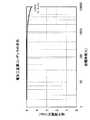
図5は各部の電圧のタイミングチャートである。図5(イ)は商用電源、図5(ロ)は電気二重層コンデンサ23の両端の電圧であるバイアス電圧、図5(ハ)は正極電圧である。 FIG. 5 is a timing chart of the voltages of the respective parts. 5A is a commercial power supply, FIG. 5B is a bias voltage that is a voltage across the electric
図5に示されるように、商用電源休止期間(a)〜(b)の間に、図5(ハ)の正極電圧は負荷抵抗により低下するが、図5(ロ)のバイアス電圧は一定のままの電圧となっている。 As shown in FIG. 5, during the commercial power supply suspension periods (a) to (b), the positive voltage in FIG. 5 (c) decreases due to the load resistance, but the bias voltage in FIG. 5 (b) is constant. The voltage remains unchanged.
このようにすることによってノーマリーON型のFETのゲートバイアス電圧は一定値に維持され、図5(ハ)のように正極電圧が低下している間でも、ゲートバイアス電圧はしっかり確保されているため、ドレイン−ソースが貫通してショート破壊することはない。 By doing so, the gate bias voltage of the normally-on type FET is maintained at a constant value, and the gate bias voltage is firmly secured even while the positive voltage is decreasing as shown in FIG. The drain-source does not penetrate to cause a short circuit breakdown.
次に、この電気二重層コンデンサの寿命を図6で示す。負荷抵抗は50MΩで電流は0.5μA常時流れた場合を想定した。容量値は4.7Fを選択した。機器の耐用年数を1200時間とすると若干バイアス電圧が下がりドレイン電流は増える傾向にあるが実使用上は問題ないと思われる。 Next, the lifetime of this electric double layer capacitor is shown in FIG. It was assumed that the load resistance was 50 MΩ and the current flowed constantly at 0.5 μA. The capacitance value was selected to be 4.7F. When the service life of the device is 1200 hours, the bias voltage tends to decrease slightly and the drain current increases, but it seems that there is no problem in practical use.
このように、ノーマリーON型のFETを用いて電源部への電力供給を一斉に遮断しても半導体が破壊することがない信頼性の高いマイクロ波処理装置を提供できるだけでなく、ドアスイッチによる二重の発振停止装置を用いたり、比較的安価な交流電流を入り切りするマイクロスイッチをドアスイッチに用いたりすることができるため、システム全体を安価に構成することができる。 In this way, not only can a highly reliable microwave processing apparatus be used in which the semiconductor is not destroyed even if power supply to the power supply unit is shut off all at once using normally-on FETs, Since a heavy oscillation stop device can be used, or a micro switch that turns on and off a relatively inexpensive alternating current can be used as a door switch, the entire system can be configured at low cost.
以上のように、本発明にかかるマイクロ波処理装置は、ドアの開閉に連動する二重発振停止装置を有し、マイクロ波の人体暴露を完全に阻止するとともに、商用電源を直接入り切りするドアスイッチを用いても、ノーマリーON方のFETを破壊することなく、信頼性の高いマイクロ波処理装置を提供することができる。 As described above, the microwave processing apparatus according to the present invention has a double oscillation stop device that interlocks with opening and closing of the door, completely prevents exposure of the microwave to the human body, and directly turns on and off the commercial power supply. Can be used to provide a highly reliable microwave processing apparatus without destroying the normally-on FET.
本発明は、電子レンジで代表されるような誘電加熱を利用した加熱装置や生ゴミ処理機、あるいは、半導体製造装置であるプラズマ電源のマイクロ波電源などの用途にも適用できる。二重安全を構成する第一のドアスイッチ22、第二のドアスイッチ14は、正弦波状の電流を入り切りする機能のため非常に廉価なマイクロスイッチを使用することができる。 The present invention can also be applied to uses such as a heating apparatus and a garbage processing machine using dielectric heating as typified by a microwave oven, or a microwave power source of a plasma power source as a semiconductor manufacturing apparatus. As the
12 パワーユニット
14 第二のドアスイッチ
16 商用電源
17 電源部
18 正極電圧供給部
19 負極電圧供給部
20 バイアス電圧供給部
21 発振部
22 第一のドアスイッチ
23 電荷蓄積部DESCRIPTION OF
Claims (3)
Translated fromJapanesePriority Applications (1)
| Application Number | Priority Date | Filing Date | Title |
|---|---|---|---|
| JP2010060624AJP2011198486A (en) | 2010-03-17 | 2010-03-17 | Microwave processing device |
Applications Claiming Priority (1)
| Application Number | Priority Date | Filing Date | Title |
|---|---|---|---|
| JP2010060624AJP2011198486A (en) | 2010-03-17 | 2010-03-17 | Microwave processing device |
Publications (1)
| Publication Number | Publication Date |
|---|---|
| JP2011198486Atrue JP2011198486A (en) | 2011-10-06 |
Family
ID=44876456
Family Applications (1)
| Application Number | Title | Priority Date | Filing Date |
|---|---|---|---|
| JP2010060624APendingJP2011198486A (en) | 2010-03-17 | 2010-03-17 | Microwave processing device |
Country Status (1)
| Country | Link |
|---|---|
| JP (1) | JP2011198486A (en) |
Cited By (2)
| Publication number | Priority date | Publication date | Assignee | Title |
|---|---|---|---|---|
| JP2013110831A (en)* | 2011-11-18 | 2013-06-06 | Fujitsu Ltd | Control circuit and electronic apparatus |
| JPWO2023162634A1 (en)* | 2022-02-24 | 2023-08-31 |
- 2010
- 2010-03-17JPJP2010060624Apatent/JP2011198486A/enactivePending
Cited By (3)
| Publication number | Priority date | Publication date | Assignee | Title |
|---|---|---|---|---|
| JP2013110831A (en)* | 2011-11-18 | 2013-06-06 | Fujitsu Ltd | Control circuit and electronic apparatus |
| JPWO2023162634A1 (en)* | 2022-02-24 | 2023-08-31 | ||
| WO2023162634A1 (en)* | 2022-02-24 | 2023-08-31 | パナソニックIpマネジメント株式会社 | Radio wave radiation device |
Similar Documents
| Publication | Publication Date | Title |
|---|---|---|
| JP2011146143A (en) | Microwave processing device | |
| US11013075B2 (en) | RF apparatus with arc prevention using non-linear devices | |
| WO2004062326A3 (en) | Low power plasma generator | |
| US20100141168A1 (en) | Class-e amplifier and lighting ballast using the amplifier | |
| WO2008091699A3 (en) | Capacitive discharge welding power supply and capacitive discharge welder using the same | |
| JP2011198486A (en) | Microwave processing device | |
| JPWO2013094095A1 (en) | Microwave heating device | |
| RU2419960C2 (en) | Microwave generator | |
| US4063132A (en) | DC powered microwave discharge in an electrodeless light source | |
| Shinoda et al. | Idealized operation of Class DE amplifier and frequency multipliers | |
| KR20220003884A (en) | Aerosol generating device which harvests energy | |
| JPS6057676B2 (en) | Power supply device for microwave discharge light source | |
| JPH0250600B2 (en) | ||
| Kuthi et al. | Marx generator using pseudospark switches | |
| JPS59114748A (en) | Microwave electric-discharge light source device | |
| WO2023162634A1 (en) | Radio wave radiation device | |
| JPS59103271A (en) | Microwave discharge light source device | |
| KR102037310B1 (en) | Cooking appliance | |
| JP2013206859A (en) | Plasma discharge lamp starting device | |
| Holt et al. | Investigation of an FCG and pulse transformer based power conditioning system | |
| JP3995756B2 (en) | Earth leakage protection relay with buzzer | |
| Kuthi et al. | Feedback stabilized pseudospark switch for fast rise Marx generator application | |
| JP2004103482A (en) | Noble gas discharge lamp lighting device | |
| JPS6021474B2 (en) | High frequency heating device | |
| KR101616719B1 (en) | Pulsed DC oscillator |