JP2011192934A - Division method for workpiece - Google Patents
Division method for workpieceDownload PDFInfo
- Publication number
- JP2011192934A JP2011192934AJP2010060002AJP2010060002AJP2011192934AJP 2011192934 AJP2011192934 AJP 2011192934AJP 2010060002 AJP2010060002 AJP 2010060002AJP 2010060002 AJP2010060002 AJP 2010060002AJP 2011192934 AJP2011192934 AJP 2011192934A
- Authority
- JP
- Japan
- Prior art keywords
- semiconductor wafer
- workpiece
- holding
- back surface
- holding table
- Prior art date
- Legal status (The legal status is an assumption and is not a legal conclusion. Google has not performed a legal analysis and makes no representation as to the accuracy of the status listed.)
- Granted
Links
Images


Classifications
- H—ELECTRICITY
- H01—ELECTRIC ELEMENTS
- H01L—SEMICONDUCTOR DEVICES NOT COVERED BY CLASS H10
- H01L21/00—Processes or apparatus adapted for the manufacture or treatment of semiconductor or solid state devices or of parts thereof
- H01L21/67—Apparatus specially adapted for handling semiconductor or electric solid state devices during manufacture or treatment thereof; Apparatus specially adapted for handling wafers during manufacture or treatment of semiconductor or electric solid state devices or components ; Apparatus not specifically provided for elsewhere
- H01L21/67005—Apparatus not specifically provided for elsewhere
- H01L21/67011—Apparatus for manufacture or treatment
- H01L21/67092—Apparatus for mechanical treatment
- B—PERFORMING OPERATIONS; TRANSPORTING
- B23—MACHINE TOOLS; METAL-WORKING NOT OTHERWISE PROVIDED FOR
- B23K—SOLDERING OR UNSOLDERING; WELDING; CLADDING OR PLATING BY SOLDERING OR WELDING; CUTTING BY APPLYING HEAT LOCALLY, e.g. FLAME CUTTING; WORKING BY LASER BEAM
- B23K26/00—Working by laser beam, e.g. welding, cutting or boring
- B23K26/36—Removing material
- B23K26/38—Removing material by boring or cutting
- B—PERFORMING OPERATIONS; TRANSPORTING
- B23—MACHINE TOOLS; METAL-WORKING NOT OTHERWISE PROVIDED FOR
- B23K—SOLDERING OR UNSOLDERING; WELDING; CLADDING OR PLATING BY SOLDERING OR WELDING; CUTTING BY APPLYING HEAT LOCALLY, e.g. FLAME CUTTING; WORKING BY LASER BEAM
- B23K26/00—Working by laser beam, e.g. welding, cutting or boring
- B23K26/36—Removing material
- B23K26/40—Removing material taking account of the properties of the material involved
- H—ELECTRICITY
- H01—ELECTRIC ELEMENTS
- H01L—SEMICONDUCTOR DEVICES NOT COVERED BY CLASS H10
- H01L21/00—Processes or apparatus adapted for the manufacture or treatment of semiconductor or solid state devices or of parts thereof
- H01L21/67—Apparatus specially adapted for handling semiconductor or electric solid state devices during manufacture or treatment thereof; Apparatus specially adapted for handling wafers during manufacture or treatment of semiconductor or electric solid state devices or components ; Apparatus not specifically provided for elsewhere
- H01L21/67005—Apparatus not specifically provided for elsewhere
- H01L21/67011—Apparatus for manufacture or treatment
- H01L21/6715—Apparatus for applying a liquid, a resin, an ink or the like
- H—ELECTRICITY
- H01—ELECTRIC ELEMENTS
- H01L—SEMICONDUCTOR DEVICES NOT COVERED BY CLASS H10
- H01L21/00—Processes or apparatus adapted for the manufacture or treatment of semiconductor or solid state devices or of parts thereof
- H01L21/67—Apparatus specially adapted for handling semiconductor or electric solid state devices during manufacture or treatment thereof; Apparatus specially adapted for handling wafers during manufacture or treatment of semiconductor or electric solid state devices or components ; Apparatus not specifically provided for elsewhere
- H01L21/683—Apparatus specially adapted for handling semiconductor or electric solid state devices during manufacture or treatment thereof; Apparatus specially adapted for handling wafers during manufacture or treatment of semiconductor or electric solid state devices or components ; Apparatus not specifically provided for elsewhere for supporting or gripping
- H01L21/687—Apparatus specially adapted for handling semiconductor or electric solid state devices during manufacture or treatment thereof; Apparatus specially adapted for handling wafers during manufacture or treatment of semiconductor or electric solid state devices or components ; Apparatus not specifically provided for elsewhere for supporting or gripping using mechanical means, e.g. chucks, clamps or pinches
- H01L21/68714—Apparatus specially adapted for handling semiconductor or electric solid state devices during manufacture or treatment thereof; Apparatus specially adapted for handling wafers during manufacture or treatment of semiconductor or electric solid state devices or components ; Apparatus not specifically provided for elsewhere for supporting or gripping using mechanical means, e.g. chucks, clamps or pinches the wafers being placed on a susceptor, stage or support
- H01L21/68728—Apparatus specially adapted for handling semiconductor or electric solid state devices during manufacture or treatment thereof; Apparatus specially adapted for handling wafers during manufacture or treatment of semiconductor or electric solid state devices or components ; Apparatus not specifically provided for elsewhere for supporting or gripping using mechanical means, e.g. chucks, clamps or pinches the wafers being placed on a susceptor, stage or support characterised by a plurality of separate clamping members, e.g. clamping fingers
- B—PERFORMING OPERATIONS; TRANSPORTING
- B23—MACHINE TOOLS; METAL-WORKING NOT OTHERWISE PROVIDED FOR
- B23K—SOLDERING OR UNSOLDERING; WELDING; CLADDING OR PLATING BY SOLDERING OR WELDING; CUTTING BY APPLYING HEAT LOCALLY, e.g. FLAME CUTTING; WORKING BY LASER BEAM
- B23K2103/00—Materials to be soldered, welded or cut
- B23K2103/50—Inorganic material, e.g. metals, not provided for in B23K2103/02 – B23K2103/26
Landscapes
- Engineering & Computer Science (AREA)
- Physics & Mathematics (AREA)
- Microelectronics & Electronic Packaging (AREA)
- General Physics & Mathematics (AREA)
- Manufacturing & Machinery (AREA)
- Computer Hardware Design (AREA)
- Condensed Matter Physics & Semiconductors (AREA)
- Power Engineering (AREA)
- Optics & Photonics (AREA)
- Plasma & Fusion (AREA)
- Mechanical Engineering (AREA)
- Dicing (AREA)
- Laser Beam Processing (AREA)
Abstract
Description
Translated fromJapanese本発明は、半導体ウェーハ等のワークを分割するワークの分割方法に関するものである。 The present invention relates to a work dividing method for dividing a work such as a semiconductor wafer.
半導体デバイス製造工程においては、略円板形状であるワークの表面に格子状に配列されたストリートと呼ばれる分割予定ラインによって複数の領域が区画され、この区画された領域にICやLSI等の回路が形成される。そして、分割予定ラインに沿ってワークを切断して回路が形成された領域を分割することにより、個々の半導体チップが製造される。 In the semiconductor device manufacturing process, a plurality of regions are partitioned by dividing lines called streets arranged in a lattice pattern on the surface of a substantially disk-shaped workpiece, and circuits such as ICs and LSIs are formed in the partitioned regions. It is formed. Then, the individual semiconductor chips are manufactured by dividing the region where the circuit is formed by cutting the work along the planned dividing lines.
ところで、分割予定ラインに沿ったワークの切断は、例えば、ダイサーと呼ばれる切削装置によって行われている。また、近年では、ワークに対して透過性を有する波長のパルス状の加工用レーザー光線(パルスレーザー)を照射するレーザー加工方法が試みられている(例えば、特許文献1を参照)。このレーザー加工方法を用いた分割方法では、例えば、ワークの一方の面側からワークの内部に集光点を合わせた状態でワークに対して透過性を有する赤外光領域のパルスレーザーを照射し、ワークの内部に分割予定ラインに沿った改質層を連続的に形成する。そして、ワークに外力を加えることにより、改質層が形成されたことで強度が低下した分割予定ラインに沿ってワークを分割している。 By the way, the cutting | disconnection of the workpiece | work along a division | segmentation planned line is performed by the cutting device called a dicer, for example. In recent years, a laser processing method for irradiating a pulsed processing laser beam (pulse laser) having a wavelength that is transparent to a workpiece has been attempted (for example, see Patent Document 1). In the dividing method using this laser processing method, for example, a pulse laser in the infrared region that is transparent to the workpiece is irradiated from the one surface side of the workpiece with the condensing point inside the workpiece. Then, a modified layer is continuously formed in the work along the line to be divided. Then, by applying an external force to the work, the work is divided along the planned dividing line whose strength has been reduced by forming the modified layer.
しかしながら、パルスレーザーを照射してこのパルスレーザーを入射させる側のワークの面(入射面)に凹凸が存在していると、空気とワークとの間で屈折が起こるので照射したパルスレーザーが十分に集光されず、加工品質が低下するという問題があった。このため、従来は、事前に入射面とするワークの裏面に研削加工を施し、入射面を平坦化する必要があった。例えば、ワークがシリコンウェーハの場合、粒度が#2000以上の砥石で入射面を研削加工する必要があった。ここで、研削加工は、ワークを薄くすること等を目的としてワークに施される加工であるが、この方法では、薄くする必要のないものにも研削加工を実施する必要があった。また、ワークの種類によっては研削加工が行えず、特許文献1のようなレーザー加工方法を適用できない場合があった。 However, if there are irregularities on the surface of the workpiece (incident surface) on which the pulse laser is irradiated and this pulse laser is incident, refraction occurs between the air and the workpiece. There was a problem that the processing quality deteriorated without being condensed. For this reason, conventionally, it has been necessary to perform a grinding process on the back surface of the work as the incident surface in advance to flatten the incident surface. For example, when the workpiece is a silicon wafer, it is necessary to grind the incident surface with a grindstone having a particle size of # 2000 or more. Here, the grinding process is a process performed on the workpiece for the purpose of thinning the workpiece. However, in this method, it is necessary to perform the grinding process even on a workpiece that does not need to be thinned. Further, depending on the type of workpiece, grinding cannot be performed, and there are cases where the laser processing method as in Patent Document 1 cannot be applied.
本発明は、上記に鑑みて為されたものであり、パルスレーザーの入射面に凹凸が存在するワークであっても、ワークの内部に改質層を形成するレーザー加工を行ってワークを分割することができるワークの分割方法を提供することを目的とする。 The present invention has been made in view of the above, and divides a workpiece by performing laser processing for forming a modified layer inside the workpiece even if the workpiece has irregularities on the incident surface of the pulse laser. An object of the present invention is to provide a method of dividing a work that can be performed.
上記した課題を解決し、目的を達成するために、本発明にかかるワークの分割方法は、入射面が凹凸を有するワークの前記入射面側から前記ワークを透過する波長のパルスレーザーを照射し、前記ワークの内部に改質層を形成して分割するワークの分割方法であって、前記パルスレーザーが透過し、該パルスレーザーに対する屈折率が前記ワークに近い塗布部材を前記入射面に塗布して前記ワークの前記入射面側を平坦化する工程と、前記塗布部材が塗布された前記ワークの前記入射面側から前記パルスレーザーを前記ワークの内部に集光点を合わせて照射し、前記ワークの内部に改質層を形成する工程と、前記ワークに外力を加えることによって、前記ワークの内部に形成された前記改質層を基点として前記ワークを分割する工程と、を含むことを特徴とする。 In order to solve the above-described problems and achieve the object, the method for dividing a workpiece according to the present invention irradiates a pulse laser having a wavelength that transmits the workpiece from the incident surface side of the workpiece having an incident surface having irregularities, A method of dividing a workpiece by forming a modified layer inside the workpiece and dividing the workpiece, wherein the pulse laser is transmitted and a coating member having a refractive index close to the workpiece is applied to the incident surface. A step of flattening the incident surface side of the workpiece, and irradiating the pulse laser from the incident surface side of the workpiece coated with the coating member to the inside of the workpiece with a converging point, A step of forming a modified layer inside, and a step of dividing the workpiece with the modified layer formed inside the workpiece as a base point by applying an external force to the workpiece. It is characterized in.
本発明によれば、パルスレーザーの入射面にその屈折率がワークに近い塗布部材を塗布することでワークの入射面側と空気との界面を平坦化し、ワークの入射面と塗布部材との界面におけるパルスレーザーの屈折の度合いを小さくすることができる。これによれば、ワーク内部の集光点に対するパルスレーザーの集光精度を向上させることができるので、パルスレーザーの入射面に凹凸が存在するワークであっても、ワーク内部に改質層を形成するレーザー加工を行ってワークを分割することができる。 According to the present invention, the interface between the incident surface of the workpiece and the coating member is flattened by applying the coating member whose refractive index is close to that of the workpiece to the incident surface of the pulse laser. The degree of refraction of the pulse laser can be reduced. According to this, since the focusing accuracy of the pulse laser to the focusing point inside the workpiece can be improved, even if the workpiece has irregularities on the incident surface of the pulse laser, a modified layer is formed inside the workpiece. The workpiece can be divided by laser processing.
以下、本発明を実施するための形態であるワークの分割方法について図面を参照して説明する。本実施の形態におけるワークの分割方法は、分割対象のワークに対して先ずパルスレーザーを照射し、ワークの内部に改質層を形成するものである。そしてその後、改質層が形成されて強度が低下したワークに外力を加えることにより、ワークを分割するものである。 Hereinafter, a method for dividing a workpiece, which is a mode for carrying out the present invention, will be described with reference to the drawings. In the work dividing method according to the present embodiment, the work to be divided is first irradiated with a pulse laser to form a modified layer inside the work. Then, the work is divided by applying an external force to the work whose strength has been reduced by forming the modified layer.
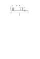
図1は、ワークの一例である半導体ウェーハ10の構成およびこの半導体ウェーハ10の内部に改質層を形成するためのレーザー加工装置1の主要部の構成を説明する概略斜視図である。図1に示すように、本実施の形態で分割対象とする半導体ウェーハ10は、略円板形状を有する。ここで、本実施の形態のレーザー加工装置1は、図1に示すように、例えば、環状フレームFの内側開口部を覆うように外周部が装着された伸張可能な合成樹脂シートからなる保持テープTに表面側が貼着され、裏面(図1中の上側の面)11が露出した状態の半導体ウェーハ10を扱う。保護テープTが貼着される半導体ウェーハ10の表面側は、図1中に破線で示すように互いに直交する分割予定ラインL(L1,L2)によって格子状に区画されており、これら区画された領域内にデバイス12が形成された構成となっている。 FIG. 1 is a schematic perspective view illustrating a configuration of a
なお、ワークの具体例は、特に限定されるものではなく、例えばシリコン(Si)やガリウムヒ素(GaAs)等の半導体ウェーハ、チップ実装用としてウェーハの裏面に設けられるDAF(Die Attach Film)等の粘着部材、あるいは半導体製品のパッケージ、セラミック、ガラス、サファイア(Al2O3)系の無機材料基板、LCDドライバー等の各種電子部品、さらにはμmオーダーの加工位置精度が要求される各種加工材料が挙げられる。The specific example of the workpiece is not particularly limited. For example, a semiconductor wafer such as silicon (Si) or gallium arsenide (GaAs), or a DAF (Die Attach Film) provided on the back surface of the wafer for chip mounting. Adhesive members or semiconductor product packages, ceramics, glass, sapphire (Al2 O3 ) inorganic material substrates, various electronic parts such as LCD drivers, and various processing materials that require processing position accuracy on the order of μm Can be mentioned.
レーザー加工装置1は、上記した半導体ウェーハ10の裏面11を入射面とし、表面側でデバイス12を区画している格子状の分割予定ラインLのそれぞれに沿うように裏面11側からパルスレーザーを照射することで、半導体ウェーハ10の内部に分割予定ラインLに沿った改質層を形成する。また、本実施の形態のレーザー加工装置1は、塗布装置100が一体に組み込まれた構成となっており、レーザー加工に先立って半導体ウェーハ10の裏面11に塗布部材を塗布し、裏面11側を平坦化する。 The laser processing apparatus 1 irradiates a pulse laser from the
先ず、塗布装置100について説明する。図2は、塗布装置100を構成する保持テーブル120の収納位置を説明する概略斜視図であり、筐体110の一部を切り欠いて筐体110の内部を示している。図1および図2に示すように、塗布装置100は、半導体ウェーハ10を保持するための保持テーブル120と、保持テーブル120によって保持された半導体ウェーハ10の裏面11に塗布部材を供給するための塗布部材供給手段140とを備える。 First, the
保持テーブル120は、半導体ウェーハ10に応じた大きさのチャックテーブルを主体とするものであり、上面である保持面121の周囲に配設されたクランプ122によって環状フレームFを固定し、不図示の吸引手段によって保持面121上で半導体ウェーハ10を吸引保持する。この保持テーブル120に対し、半導体ウェーハ10は、図1に示すように、不図示の搬入出手段によって裏面11が露出するように保持テープTを下にして搬入され(矢印A1)、保持面121上に載置されて吸引保持される。 The holding table 120 is mainly a chuck table having a size corresponding to the
このように保持面121上で半導体ウェーハ10を保持する保持テーブル120は、円筒状の回転部130の上端に配設されている。この回転部130は、内部に配設された不図示のパルスモータ等を含み、鉛直方向(Z軸方向)を回転軸として回転自在な構成となっている。さらに、保持テーブル120は、この回転部130を介して不図示の昇降部によりZ軸方向へ上下動自在に支持されており、保持面121は、図1に示すように筐体110の上面高さとなる塗布位置と、図2に示すように塗布位置から下降して筐体110の内部に収納された収納位置とに選択的に位置付けられる。ここで、筐体110は、上下動自在な保持テーブル120を収容し得る大きさの上方開口の箱状を有し、回転部130や不図示の昇降部は、この筐体110内に収容されている。 As described above, the holding table 120 that holds the
塗布部材供給手段140は、図2に示すように、筐体110上面の開口近傍に配設されて鉛直方向を回転軸とする回転を自在に行う支軸141と、この支軸141の上端側に一端が連結されたアーム142と、このアーム142の他端側に噴出口が下を向くようにして設けられたノズル143とを備え、この他に、塗布部材供給源やこの塗布部材供給源からの塗布部材をノズル143に導くパイプ等を含む。この塗布部材供給手段140は、後述する塗布工程において支軸141の回転によってアーム142が回動し、塗布位置に位置付けられた保持面121の中心近傍上方にノズル143が移動するようになっており、ノズル143から塗布部材を噴出して保持面121上の半導体ウェーハ10の裏面11に供給する。 As shown in FIG. 2, the application member supply means 140 is arranged near the opening on the top surface of the
また、この塗布装置100は、レーザー加工後の半導体ウェーハ10の洗浄を行う洗浄装置としても機能し、収納位置に位置付けられた保持面121上の半導体ウェーハ10の裏面11に例えば洗浄用の水(洗浄水)を噴出する洗浄水供給ノズル150およびエアー供給源からのエアーを噴出するエアーノズル160を備えている。 The
そして、以上のように構成される塗布装置100が一体に組み込まれたレーザー加工装置1は、図1に示すように、半導体ウェーハ10を保持するための保持テーブル2と、この保持テーブル2をX軸方向(加工送り方向)およびY軸方向(割り出し送り方向)に移動させるための保持テーブル駆動手段4と、保持テーブル2によって保持された半導体ウェーハ10の裏面11側からパルスレーザーを照射するためのレーザー照射手段5とを備える。 The laser processing apparatus 1 in which the
保持テーブル2は、塗布装置100の保持テーブル120と同様に、半導体ウェーハ10に応じた大きさのチャックテーブルを主体とするものであり、上面である保持面21の周囲に配設されたクランプ22によって環状フレームFを固定し、不図示の吸引手段によって保持面21上に載置された半導体ウェーハ10を吸引保持する。保持テーブル2に対しても、半導体ウェーハ10は、裏面11が露出するように保持テープTを下にして搬入され、保持面21上に載置されて吸引保持される。 Similar to the holding table 120 of the
ここで、保持テーブル2には、塗布装置100によって裏面11に塗布部材が塗布された半導体ウェーハ10が搬入される。塗布装置100の保持テーブル120と保持テーブル2との間の半導体ウェーハ10の搬送は、搬送手段6によって行われる。搬送手段6は、一般に使用されている搬送手段と同一の構成でよく、例えば一対の案内レール61の間に平行に延設されたボールネジ62やこのボールネジ62を回転駆動するパルスモータ63、案内レール61に摺動自在に係合し、パルスモータ63の駆動によって保持テーブル120の上方と保持テーブル2の上方との間を案内レール61に沿って移動する移動ブロック64、移動ブロック64の下端に取り付けられ、環状フレームFを吸引保持する搬送パッド651を上下方向に昇降自在に保持する保持手段65等を備える。 Here, the
以上のように保持面21上で半導体ウェーハ10を保持する保持テーブル2は、円筒部材3の上端に設けられ、円筒部材3内に配設された不図示のパルスモータによって鉛直軸を軸中心として回転自在な構成となっている。 As described above, the holding table 2 that holds the
保持テーブル駆動手段4は、2段の滑動ブロック41,42を備え、保持テーブル2は、円筒部材3を介してこれら2段の滑動ブロック41,42の上に搭載されている。また、保持テーブル駆動手段4は、ボールネジ431やパルスモータ432等で構成された割り出し送り手段43を備え、滑動ブロック41は、この割り出し送り手段43によってY軸方向への移動が自在である。そして、割り出し送り手段43が駆動して滑動ブロック41が移動し、後述するレーザー照射手段5に対して保持テーブル2がY軸方向に移動することで、滑動ブロック41に搭載された保持テーブル2とレーザー照射手段5とをY軸方向に沿って相対的に移動させる。 The holding table driving means 4 includes two stages of sliding
さらに、保持テーブル駆動手段4は、ボールネジ441やパルスモータ442等で構成された加工送り手段44を備え、滑動ブロック42は、この加工送り手段44によってX軸方向への移動が自在である。そして、加工送り手段44が駆動して滑動ブロック42が移動し、レーザー照射手段5に対して保持テーブル2がX軸方向に移動することで、滑動ブロック42に搭載された保持テーブル2とレーザー照射手段5とをX軸方向に沿って相対的に移動させる。 Further, the holding table driving means 4 includes a machining feed means 44 constituted by a
また、割り出し送り手段43に対しては、保持テーブル2の割り出し送り量を検出するための割り出し送り量検出手段45が付設されている。割り出し送り量検出手段45は、Y軸方向に沿って配設されたリニアスケールや、滑動ブロック41に配設されて滑動ブロック41とともに移動することでリニアスケールを読み取る読み取りヘッド等で構成される。同様に、加工送り手段44に対しては、保持テーブル2の加工送り量を検出するための加工送り量検出手段46が付設されている。この加工送り量検出手段46は、X軸方向に沿って配設されたリニアスケールや、滑動ブロック42に配設されて滑動ブロック42とともに移動することでリニアスケールを読み取る読み取りヘッド等で構成される。 The index feed means 43 is additionally provided with an index feed amount detection means 45 for detecting the index feed amount of the holding table 2. The index feed amount detection means 45 includes a linear scale disposed along the Y-axis direction, a reading head that is disposed in the sliding
レーザー照射手段5は、レーザー照射ユニット51と、保持テーブル2の上方でレーザー照射ユニット51を支持する支持部材53とを備える。 The laser irradiation means 5 includes a
レーザー照射ユニット51は、保持面21上の半導体ウェーハ10に対してパルスレーザーを照射し、分割予定ラインLに沿って溝を形成するためのものであり、その下端部に保持面21上の半導体ウェーハ10の裏面11と対向するように配設された集光器52を具備している。集光器52は、レーザー照射ユニット51の内部に配設されたパルスレーザー発振手段によって発振されるパルスレーザーを保持面21上の半導体ウェーハ10に向けて集光させるための集光レンズが内部に配設されたものである。パルスレーザー発振手段は、例えばYAGレーザー発振器やYVO4レーザー発振器からなり、集光器52の鉛直下方に位置付けられる半導体ウェーハ10の裏面11側から、半導体ウェーハ10を透過する所定波長(例えば1064nm)のパルスレーザーを発振する。 The
なお、支持部材53は、レーザー照射ユニット51をZ軸方向に移動自在に支持しており、集光器52に内蔵された集光レンズを保持面21に対して垂直に移動させることができる。このように、レーザー照射手段5は、集光レンズによって集光されるパルスレーザーの集光点位置(Z位置)の調整が可能な構成とされている。 The
以上のように構成されるレーザー加工装置1は、レーザー加工装置1を構成する各部の動作を制御してレーザー加工装置1を統括的に制御する制御手段7を備える。制御手段7は、レーザー加工装置1の動作に必要な各種データを保持するメモリを内蔵したマイクロコンピュータ等で構成され、この制御手段7の制御のもと、レーザー加工装置1は、保持工程、塗布工程および改質層形成工程を実施する。 The laser processing apparatus 1 configured as described above includes a control unit 7 that controls the operation of each part of the laser processing apparatus 1 and controls the laser processing apparatus 1 in an integrated manner. The control means 7 is composed of a microcomputer or the like with a built-in memory for holding various data necessary for the operation of the laser processing apparatus 1. Under the control of the control means 7, the laser processing apparatus 1 performs the holding process, the coating process. A process and a modified layer formation process are implemented.
ここで、本実施の形態のワークの分割方法において上記したレーザー加工装置1が行うレーザー加工の概要について、従来の問題点と対比しながら説明する。図3は、従来の問題点を説明する説明図であり、半導体ウェーハ10の断面を示すとともに、この断面の一部を拡大して内部に照射されるパルスレーザーの光路を一点鎖線で示している。一方、図4は、本実施の形態のレーザー加工の概要を説明する説明図であり、図3と同様に、半導体ウェーハ10の断面を示すとともに、この断面の一部を拡大して内部に照射されるパルスレーザーの光路を一点鎖線で示している。 Here, an outline of laser processing performed by the laser processing apparatus 1 in the workpiece dividing method of the present embodiment will be described in comparison with conventional problems. FIG. 3 is an explanatory diagram for explaining a conventional problem, showing a cross section of the
本実施の形態では、分割対象とする半導体ウェーハ10の裏面11に凹凸が存在することを想定している。ここで、空気と半導体ウェーハ10とでは、パルスレーザーに対する屈折率が異なる。このため、半導体ウェーハ10に対して裏面11側からパルスレーザーを照射すると、パルスレーザーの光路は、空気と半導体ウェーハ10との界面において屈折する。このとき、図3に示すように、半導体ウェーハ10の裏面11の凹凸が存在する部分に直接パルスレーザーを照射してしまうと、その照射領域内で裏面11の高さがばらついているため、図3中の拡大部分において破線E2で囲って示すように、パルスレーザーが十分に集光されないという問題が生じる。 In the present embodiment, it is assumed that unevenness exists on the
これに対し、本実施の形態のワークの分割方法では、図4に示すように、レーザー加工に先立って半導体ウェーハ10の裏面11の全面に塗布部材13を塗布し、裏面11側を平坦化するようになっている(後述する塗布工程)。塗布部材としては、パルスレーザーに対する屈折率が半導体ウェーハ10と大きく異なるものは適切ではなく、半導体ウェーハ10に近いものがよい。これによれば、半導体ウェーハ10の裏面11側と空気との界面を平坦化することができ、半導体ウェーハ10の裏面11と塗布部材13との界面におけるパルスレーザーの屈折の度合いを小さくすることができるので、図4中の拡大部分において破線E3で囲って示すように、半導体ウェーハ10内部の所定の深さ位置として予め設定される集光点P3にパルスレーザーを十分に集光させることが可能となる。 On the other hand, in the workpiece dividing method of the present embodiment, as shown in FIG. 4, the
具体的な材料としては、例えばポリイミド、光学プラスチック、PVA(Poly Vinyl Alcohol)等が挙げられる。なお、分割対象とするワーク(ここでは半導体ウェーハ10)のパルスレーザーに対する屈折率は、ワークの種類によって異なる。例えば、シリコンの屈折率は4.0前後であり、シリコンウェーハを分割対象とする場合には、パルスレーザーに対する屈折率が4.0に近い塗布部材を選択するのがよい。また、サファイアの屈折率は1.9前後であり、サファイア基板を分割対象とする場合には、パルスレーザーに対する屈折率が1.9に近い塗布部材を選択するのがよい。 Specific examples of the material include polyimide, optical plastic, and PVA (Poly Vinyl Alcohol). In addition, the refractive index with respect to the pulse laser of the workpiece | work (here semiconductor wafer 10) made into a division | segmentation object changes with kinds of workpiece | work. For example, the refractive index of silicon is around 4.0, and when a silicon wafer is to be divided, an application member having a refractive index close to 4.0 with respect to a pulse laser is preferably selected. In addition, the refractive index of sapphire is around 1.9, and when a sapphire substrate is to be divided, it is preferable to select an application member having a refractive index close to 1.9 with respect to the pulse laser.
より好ましくは、パルスレーザーに対する屈折率が、空気よりも分割対象とするワーク(ここでは半導体ウェーハ10)に近いものを選ぶのがよい。塗布部材のパルスビームに対する屈折率が空気に対する値よりもワークに対する値に近ければ、ワークの裏面と塗布部材との界面におけるパルスレーザーの屈折の度合いを塗布部材と空気との界面におけるパルスレーザーの屈折の度合いよりも小さくすることができ、ワーク内部の集光点にパルスレーザーをより精度良く集光させることが可能となる。これによれば、ワークに対するレーザー加工をより高品質で行うことができ、ワークの分割精度を向上させることができる。なお、本実施の形態のレーザー加工で用いるパルスレーザーに対する空気(0℃,1気圧)の屈折率は、約1.0である。したがって、シリコンの屈折率が4.0前後であることを踏まえると、大体1.0以上7.0未満の屈折率を持つ塗布部材を採用することで加工性を向上させることができると考えられる。もちろん、屈折率が4.0に近づくほど加工性の向上が期待できる。 More preferably, the refractive index for the pulse laser is closer to that of the work to be divided (here, the semiconductor wafer 10) than air. If the refractive index for the pulse beam of the coating member is closer to the value for the workpiece than for the air, the degree of refraction of the pulse laser at the interface between the back surface of the workpiece and the coating member is determined as the refraction of the pulse laser at the interface between the coating member and air. This makes it possible to focus the pulse laser more accurately on the condensing point inside the workpiece. According to this, laser processing on the workpiece can be performed with higher quality, and the division accuracy of the workpiece can be improved. Note that the refractive index of air (0 ° C., 1 atm) with respect to the pulse laser used in the laser processing of the present embodiment is about 1.0. Therefore, considering that the refractive index of silicon is around 4.0, it is considered that the workability can be improved by employing a coating member having a refractive index of approximately 1.0 or more and less than 7.0. . Of course, the workability can be expected to improve as the refractive index approaches 4.0.
ここで、本発明の発明者等は、シリコンウェーハの裏面に屈折率が1.5程度の塗布部材を1.3um程の厚みで塗布して裏面を平坦化した上で、裏面側からパルスレーザーを照射する実験を行った。また、比較のために、塗布部材を塗布せずにシリコンウェーハの裏面側から直接パルスレーザーを照射し、レーザー加工を行った。この結果、塗布部材を塗布しない場合と比べて改質層の形成を良好に行えた。 Here, the inventors of the present invention apply a coating member having a refractive index of about 1.5 to the back surface of the silicon wafer with a thickness of about 1.3 μm to flatten the back surface, and then apply a pulse laser from the back surface side. The experiment which irradiates was conducted. For comparison, laser processing was performed by directly irradiating a pulse laser from the back side of the silicon wafer without applying the application member. As a result, the modified layer was formed better than when the application member was not applied.
次に、本実施の形態におけるワークの分割方法の具体的な工程について説明する。本実施の形態におけるワークの分割方法では、先ず、以上のように構成されるレーザー加工装置1によって保持工程、塗布工程および改質層形成工程を順に実施する。続いて、分割工程を実施し、分割予定ラインのそれぞれに沿ってワークである半導体ウェーハ10を分割する。その後、塗布部材除去工程を実施し、塗布工程で半導体ウェーハ10の裏面11に塗布した塗布部材を除去する。 Next, specific steps of the work dividing method according to the present embodiment will be described. In the workpiece dividing method according to the present embodiment, first, the holding process, the coating process, and the modified layer forming process are sequentially performed by the laser processing apparatus 1 configured as described above. Subsequently, a dividing step is performed to divide the
図5〜図9は、本実施の形態におけるワークの分割方法の各工程を説明する図であり、各工程における分割対象の半導体ウェーハ10の断面図を示している。具体的には、図5は、本実施の形態の保持工程を説明する説明図であり、図6は、塗布工程を説明する説明図であり、図7は、改質層形成工程を説明する説明図であり、図8は、分割工程を説明する説明図であり、図9は、塗布部材除去工程を説明する説明図である。 5 to 9 are diagrams for explaining each process of the workpiece dividing method according to the present embodiment, and show cross-sectional views of the
(保持工程)
保持工程に先立ち、塗布装置100において不図示の昇降部が保持テーブル120を塗布位置に位置付けるとともに、不図示の搬入出手段が裏面11を上にした状態で半導体ウェーハ10を保持テーブル120に搬入し、保持面121上に載置する。そして、保持工程では、保持テーブル120の吸引手段(不図示)が駆動し、保持面121上で半導体ウェーハ10をその表面に貼着された保持テープTを介して吸引保持する。これにより、図5に示すように、半導体ウェーハ10は、裏面11が露出するように保持される。また、この保持工程では、塗布部材供給手段140が駆動し、支軸141を回転させることによってアーム142を回動させ、保持面121の中心近傍上方にノズル143を移動させる。(Holding process)
Prior to the holding step, the lifting unit (not shown) in the
(塗布工程)
続く塗布工程では、塗布部材供給手段140が駆動し、ノズル143から所定量の塗布部材を噴出させることで保持面121上の半導体ウェーハ10の裏面11に塗布部材を供給する。続いて、不図示の昇降部が駆動して保持テーブル120を下降させ、保持テーブル120を収納位置に位置付ける。その後、回転部130が駆動し、保持テーブル120を所定の回転速度で所定の時間回転させることで、遠心力によって裏面11の全面に塗布部材を広げる。保持テーブル120の回転速度および回転時間は、塗布部材の膜厚に応じて適宜設定する。膜厚についても適宜設定できるが、半導体ウェーハ10の裏面11の凹凸を平坦化するために必要な最小限の膜厚であることが望ましい。例えば本発明の発明者等は、1.3um程度の塗布を行ったところ、良好な加工結果が得られた。この結果、図6に示すように、裏面11の全面に所望の膜厚で塗布部材13が塗布され、裏面11側が平坦化される。なお、半導体ウェーハ10の裏面11に供給された塗布部材の大半は保持テーブル120の回転による遠心力によって半導体ウェーハ10外に飛散するが、このとき、保持テーブル120は筐体110内部の位置である収納位置に位置付けられており、塗布部材13が筐体110外に飛散することがない。(Coating process)
In the subsequent coating process, the coating
(改質層形成工程)
改質層形成工程に先立ち、塗布装置100では、不図示の昇降部が保持テーブル120を塗布位置に位置付ける。続いて、搬送手段6が駆動し、保持面121上の半導体ウェーハ10を保持テーブル2へと搬送して保持面21上に載置する。そして、保持テーブル2の吸引手段(不図示)が駆動し、保持面21上で半導体ウェーハ10をその表面に貼着された保持テープTを介して吸引保持する。その後、円筒部材3内に配設された不図示のパルスモータが駆動し、保持面21上の半導体ウェーハ10の向きを、その表面の互いに直交するうちの一方の分割予定ラインがX軸方向に沿う向きに調整する。そして、改質層形成工程では、保持テーブル駆動手段4が駆動して保持テーブル2をX軸方向および/またはY軸方向に移動させ、直交するうちの一方の分割予定ラインの1つを加工対象の分割予定ラインとして集光器52の鉛直下方に位置付ける。(Modified layer formation process)
Prior to the modified layer forming step, in the
なお、これに先立ち、半導体ウェーハ10の表面の分割予定ラインを検出する必要があるが、半導体ウェーハ10は、裏面11が露出するように保持面21上で保持されている。したがって、例えば半導体ウェーハ10がシリコンウェーハの場合には、赤外線カメラ(不図示)を用いて保持面21上の半導体ウェーハ10を透過させて半導体ウェーハ10の表面側を撮像し、得られた画像データにパターンマッチング等の画像処理を施すことで分割予定ラインを検出する。そして、このように分割予定ラインを検出することで集光器52の鉛直下方に加工対象の分割予定ラインを位置付ける。ただし、ここでは、半導体ウェーハ10の表面に設定された分割予定ラインが検出できればよく、半導体ウェーハ10の種類に応じて例えば可視光のカメラ等を適宜選択して用いることとしてよい。 Prior to this, it is necessary to detect a division line on the surface of the
続いて、パルスレーザーの集光点が半導体ウェーハ10内部の所定の深さ位置となるように予め設定されたZ位置に支持部材53を移動させ、半導体ウェーハ10内部の所定の深さ位置に集光レンズの集光点を合わせる。そして、保持テーブル2をX軸方向に加工送りしながらレーザー照射ユニット51によって順次パルスレーザーを照射する。これにより、パルスレーザーが半導体ウェーハ10内部の所定の深さ位置に集光された状態で分割予定ラインに沿って照射され、この結果、半導体ウェーハ10の内部に加工対象の分割予定ラインに沿って改質層が形成される。 Subsequently, the
その後は、順次隣接する分割予定ラインを集光器52の鉛直下方に位置付けて加工対象を移しながら、分割予定ラインのそれぞれに沿って改質層を形成する。直交する一方の分割予定ライン全てに改質層を形成したならば、保持テーブル2を90度回転させることで他方の分割予定ラインがX軸方向に沿うように半導体ウェーハ10の姿勢を変更する。そして、他方の分割予定ラインを順次集光器52の鉛直下方に位置付けて加工対象を移しながら、この他方の分割予定ラインのそれぞれに沿って改質層を形成する。 After that, the modified layer is formed along each of the planned division lines while sequentially positioning adjacent division planned lines vertically below the
ここで、改質層とは、密度や屈折率、機械的強度、あるいはその他の物理的特性が周囲とは異なる状態となった領域のことをいう。例えば、溶融処理領域、クラック領域、絶縁破壊領域、屈折率変化領域等が挙げられ、これらが混在した領域を含む。 Here, the modified layer refers to a region where the density, refractive index, mechanical strength, or other physical characteristics are different from the surroundings. For example, a melt treatment region, a crack region, a dielectric breakdown region, a refractive index change region, and the like are included, and a region where these are mixed is included.
以上説明した改質層形成工程により、半導体ウェーハ10の内部には、図7に示すように、分割予定ラインのそれぞれに沿って改質層14が形成されていく。なお、図7に示す断面は、保持面21上の半導体ウェーハ10の例えばY軸方向に沿った断面を示しており、改質層形成工程によってY軸方向に直交するX軸方向に沿った分割予定ライン(紙面と直交する方向に沿った分割予定ライン)に沿って半導体ウェーハ10の内部に形成された改質層14を示している。 By the modified layer forming process described above, the modified
(分割工程)
分割工程では、半導体ウェーハ10に外力を加え、改質層14を基点として半導体ウェーハ10を分割する。この分割工程は、分割装置によって実施される。ここで、分割装置は、半導体ウェーハ10の表面に貼着された保持テープTの終端を引き伸ばして保持テープTを拡張させることにより、半導体ウェーハ10に対して放射状に引張力を作用させるものである。(Division process)
In the dividing step, an external force is applied to the
分割工程に先立ち、不図示の分割装置を構成する保持テーブルによって改質層14が形成された半導体ウェーハ10を保持する。この保持テーブルは、保持テーブル2等と同様に上面である保持面上で半導体ウェーハ10をその表面に貼着された保持テープTを介して吸引保持するものであり、この保持テーブルに対し、半導体ウェーハ10は、裏面11を上にして搬入される。そして、分割工程では、分割装置によって図8中に矢印A41、A42に示すように保持テープTを拡張させることで半導体ウェーハ10に外力を加え、改質層14が形成されたことで強度が低下している分割予定ラインに沿って半導体ウェーハ10を破断し、チップ10aに分割する。この結果、半導体ウェーハ10は、個々のデバイスに分離(個片化)される。 Prior to the dividing step, the
(塗布部材除去工程)
塗布部材除去工程では、図8に示して説明したように分割されたチップ10aの裏面11側を洗浄液で洗浄し、各チップ10aそれぞれの裏面11から塗布部材13aを除去する。洗浄液は、塗布部材の材料に応じたものを選択すればよい。この結果、図9に示すように、チップ10aの裏面11側に存在していた塗布部材が除去されて裏面11aが露出する。(Applying member removal process)
In the coating member removing step, the
なお、塗布部材13としてPVA等の水溶性の材料を用いる場合には、塗布部材除去工程をレーザー加工装置1で実施することが可能である。すなわち、上記したように、レーザー加工装置1を構成する塗布装置100は洗浄装置としての機能を有しており、分割工程後の半導体ウェーハ10を保持テーブル120に搬入することで塗布部材除去工程をレーザー加工装置1で実施することが可能である。また、ここでは、分割工程で半導体ウェーハ10をチップ10aに分割した後、塗布部材除去工程で各チップ10aそれぞれの裏面11から塗布部材13aを除去することとしたが、分割工程の前に塗布部材除去工程を実施し、半導体ウェーハ10の裏面11から塗布部材13を除去した後で分割工程を実施することとしてもよい。この場合も、塗布部材13としてPVA等の水溶性の材料を用いる場合には、改質層形成工程後の半導体ウェーハ10を搬送手段6によって保持テーブル120に搬送することで、塗布部材除去工程をレーザー加工装置1で実施することができる。 When a water-soluble material such as PVA is used as the
この場合の塗布部材除去工程では、先ず、分割工程後または改質層形成工程後の半導体ウェーハ10を保持テーブル120の保持面121上に載置する。続いて、保持テーブル120の吸引手段(不図示)が駆動し、保持面121上で半導体ウェーハ10をその表面に貼着された保持テープTを介して吸引保持する。そして、不図示の昇降部が駆動して保持テーブル120を下降させ、保持テーブル120を収納位置に位置付ける。また、このように収納位置に位置付けた保持テーブル120の保持面121上方に洗浄水供給ノズル150およびエアーノズル160を位置付ける。その後、回転部130が駆動して保持テーブル120を回転させるとともに、洗浄水供給ノズル150およびエアーノズル160から洗浄水およびエアーを半導体ウェーハ10の裏面11に噴出させる。これにより、半導体ウェーハ10の裏面11が洗浄され、裏面11から塗布部材が除去される。 In the application member removing step in this case, first, the
以上説明したように、本実施の形態では、パルスレーザーに対する屈折率が例えば半導体ウェーハ10に近い塗布部材を半導体ウェーハ10の裏面11に塗布し、半導体ウェーハ10の裏面11側を平坦化することとした。そして、このように平坦化した裏面11側からパルスレーザーを照射して半導体ウェーハ10の内部に分割予定ラインに沿った改質層を形成することとした。これによれば、パルスレーザーを半導体ウェーハ10内部の集光点に十分集光させることができ、裏面11に凹凸が存在する半導体ウェーハ10の内部に改質層を形成するレーザー加工を行い、形成した改質層を基点として半導体ウェーハ10を分割することができる。したがって、従来のように薄くする必要のないワークに研削加工を実施し、裏面を平坦化する必要がない。また、研削加工を行うことができないワークであっても、裏面を平坦化することなくワークの内部に改質層を形成するレーザー加工を行うことができる。 As described above, in the present embodiment, a coating member whose refractive index with respect to the pulse laser is, for example, close to that of the
また、分割工程で半導体ウェーハ10を分割する際には加工屑が発生する場合があり、発生した加工屑が裏面11に付着すると、デバイスの品質に影響を与える場合がある。本実施の形態によれば、半導体ウェーハ10の裏面11に塗布された塗布部材が保護膜となり、前述のような分割工程における加工屑の発生からデバイスを保護する役割も果たす。 Further, when the
また、本実施の形態では、半導体ウェーハ10の裏面11を入射面とした。このように裏面を入射面としてレーザー加工を行う場合としては、例えばMEMS(Micro Electro Mechanical Systems)等のように表面に構造物があり、表面側からパルスレーザーを入射させてこのパルスレーザーを内部に集光させることができないワークを分割対象とする場合や、例えばデバイスとして発光層が表面に形成されたサファイア基板のように表面側に形成されたデバイスにパルスレーザーを照射したくないワークを分割対象とする場合等が挙げられる。ただし、実際の加工においては、裏面側からに限らず、表面側からパルスレーザーを照射してレーザー加工を行い、内部に改質層を形成する場合もある。本発明は、このようにワークの表面を入射面としてレーザー加工を行う場合にも同様に適用が可能である。 In the present embodiment, the
以上のように、本発明のワークの分割方法は、パルスレーザーの入射面に凹凸が存在するワークであっても、ワークの内部に改質層を形成するレーザー加工を行ってワークを分割するのに適している。 As described above, the work dividing method according to the present invention divides a work by performing laser processing to form a modified layer inside the work even if the work has unevenness on the incident surface of the pulse laser. Suitable for
1 レーザー加工装置
100 塗布装置
120 保持テーブル
130 回転部
140 塗布部材供給手段
143 ノズル
2 保持テーブル
4 保持テーブル駆動手段
5 レーザー照射手段
51 レーザー照射ユニット
52 集光器
6 搬送手段
7 制御手段
10 半導体ウェーハ
12 デバイス
13 塗布部材
14 改質層
10a チップ
L(L1,L2) 分割予定ライン
T 保持テープDESCRIPTION OF SYMBOLS 1
Claims (1)
Translated fromJapanese前記パルスレーザーが透過し、該パルスレーザーに対する屈折率が前記ワークに近い塗布部材を前記入射面に塗布して前記ワークの前記入射面側を平坦化する工程と、
前記塗布部材が塗布された前記ワークの前記入射面側から前記パルスレーザーを前記ワークの内部に集光点を合わせて照射し、前記ワークの内部に改質層を形成する工程と、
前記ワークに外力を加えることによって、前記ワークの内部に形成された前記改質層を基点として前記ワークを分割する工程と、
を含むことを特徴とするワークの分割方法。Irradiating a pulse laser having a wavelength that transmits the workpiece from the incident surface side of the workpiece having an uneven incident surface, and forming a modified layer inside the workpiece to divide the workpiece,
A step of flattening the incident surface side of the workpiece by transmitting the pulse laser and applying an application member having a refractive index with respect to the pulse laser close to the workpiece on the incident surface;
Irradiating the inside of the work with a focused point from the incident surface side of the work on which the application member is applied, and forming a modified layer inside the work; and
Dividing the workpiece by applying an external force to the workpiece based on the modified layer formed inside the workpiece; and
A method for dividing a workpiece characterized by comprising:
Priority Applications (2)
| Application Number | Priority Date | Filing Date | Title |
|---|---|---|---|
| JP2010060002AJP5710133B2 (en) | 2010-03-16 | 2010-03-16 | How to divide work |
| US13/048,465US8592717B2 (en) | 2010-03-16 | 2011-03-15 | Method of dividing a workpiece having an uneven surface |
Applications Claiming Priority (1)
| Application Number | Priority Date | Filing Date | Title |
|---|---|---|---|
| JP2010060002AJP5710133B2 (en) | 2010-03-16 | 2010-03-16 | How to divide work |
Publications (2)
| Publication Number | Publication Date |
|---|---|
| JP2011192934Atrue JP2011192934A (en) | 2011-09-29 |
| JP5710133B2 JP5710133B2 (en) | 2015-04-30 |
Family
ID=44646403
Family Applications (1)
| Application Number | Title | Priority Date | Filing Date |
|---|---|---|---|
| JP2010060002AActiveJP5710133B2 (en) | 2010-03-16 | 2010-03-16 | How to divide work |
Country Status (2)
| Country | Link |
|---|---|
| US (1) | US8592717B2 (en) |
| JP (1) | JP5710133B2 (en) |
Cited By (14)
| Publication number | Priority date | Publication date | Assignee | Title |
|---|---|---|---|---|
| JP2013207170A (en)* | 2012-03-29 | 2013-10-07 | Disco Abrasive Syst Ltd | Method for dividing device wafer |
| JP2014225562A (en)* | 2013-05-16 | 2014-12-04 | 株式会社ディスコ | Optical device wafer processing method |
| JP2015115573A (en)* | 2013-12-16 | 2015-06-22 | 株式会社東京精密 | Laser dicing method |
| JP2015204367A (en)* | 2014-04-14 | 2015-11-16 | 株式会社ディスコ | Processing method of optical device wafer |
| JP2015225909A (en)* | 2014-05-27 | 2015-12-14 | 株式会社ディスコ | Processing method of wafer |
| JP2015226924A (en)* | 2014-06-02 | 2015-12-17 | 株式会社ディスコ | Chip manufacturing method |
| JP2016076522A (en)* | 2014-10-02 | 2016-05-12 | 株式会社ディスコ | Wafer processing method |
| JP2016164924A (en)* | 2015-03-06 | 2016-09-08 | 株式会社ディスコ | Single crystal substrate processing method |
| KR20170055909A (en)* | 2015-11-12 | 2017-05-22 | 가부시기가이샤 디스코 | METHOD OF SEPARATING SiC SUBSTRATE |
| JP2018026673A (en)* | 2016-08-09 | 2018-02-15 | 株式会社ディスコ | Wafer processing method |
| JP2018101678A (en)* | 2016-12-20 | 2018-06-28 | 株式会社ディスコ | Workpiece processing method |
| JP2019145665A (en)* | 2018-02-21 | 2019-08-29 | 株式会社ディスコ | Wafer division method |
| JP2019161166A (en)* | 2018-03-16 | 2019-09-19 | 株式会社ディスコ | Wafer processing method |
| JP2021089974A (en)* | 2019-12-04 | 2021-06-10 | 株式会社ディスコ | Laser processing method |
Families Citing this family (8)
| Publication number | Priority date | Publication date | Assignee | Title |
|---|---|---|---|---|
| US8933367B2 (en)* | 2011-02-09 | 2015-01-13 | Sumitomo Electric Industries, Ltd. | Laser processing method |
| JP5886603B2 (en)* | 2011-11-11 | 2016-03-16 | 株式会社ディスコ | Processing method of optical device wafer |
| JP5964580B2 (en)* | 2011-12-26 | 2016-08-03 | 株式会社ディスコ | Wafer processing method |
| CN105916626A (en)* | 2013-12-05 | 2016-08-31 | 伊雷克托科学工业股份有限公司 | Method and apparatus for internally marking a substrate having a rough surface |
| JP6506520B2 (en)* | 2014-09-16 | 2019-04-24 | 株式会社ディスコ | SiC slicing method |
| CN113508003B (en)* | 2019-03-06 | 2022-12-27 | 三菱电机株式会社 | Disassembling and assembling device, machining machine and machining head |
| CN112692435A (en)* | 2019-10-23 | 2021-04-23 | 大族激光科技产业集团股份有限公司 | Ultrafast laser-based ground glass inner miniature two-dimensional code inner carving method and system |
| JP7517936B2 (en)* | 2020-10-01 | 2024-07-17 | 株式会社ディスコ | Processing Equipment |
Citations (6)
| Publication number | Priority date | Publication date | Assignee | Title |
|---|---|---|---|---|
| JP2004160493A (en)* | 2002-11-13 | 2004-06-10 | Disco Abrasive Syst Ltd | Laser processing method |
| JP2007066951A (en)* | 2005-08-29 | 2007-03-15 | Seiko Epson Corp | LAMINATE PROCESSING METHOD, LAMINATE, DEVICE MANUFACTURING METHOD, DEVICE, INKJET RECORDING APPARATUS |
| JP2007123404A (en)* | 2005-10-26 | 2007-05-17 | Furukawa Electric Co Ltd:The | Dicing tape and semiconductor wafer dicing method |
| JP2007136482A (en)* | 2005-11-16 | 2007-06-07 | Denso Corp | Apparatus for dividing semiconductor substrate |
| JP2008006379A (en)* | 2006-06-29 | 2008-01-17 | Disco Abrasive Syst Ltd | Protective coating method |
| JP2009260211A (en)* | 2008-03-26 | 2009-11-05 | Hitachi Chem Co Ltd | Method of manufacturing semiconductor device |
Family Cites Families (10)
| Publication number | Priority date | Publication date | Assignee | Title |
|---|---|---|---|---|
| JP3408805B2 (en) | 2000-09-13 | 2003-05-19 | 浜松ホトニクス株式会社 | Cutting origin region forming method and workpiece cutting method |
| EP2400539B1 (en)* | 2002-03-12 | 2017-07-26 | Hamamatsu Photonics K.K. | Substrate dividing method |
| US20050000952A1 (en)* | 2003-05-19 | 2005-01-06 | Harter Donald J. | Focusless micromachining |
| EP1550527A1 (en)* | 2003-12-30 | 2005-07-06 | Advanced Laser Separation International (ALSI) B.V. | Method of and arrangement for separating semiconductor elements formed in a wafer of semiconductor material, and semiconductor element separated therewith |
| US7303977B2 (en)* | 2004-11-10 | 2007-12-04 | Intel Corporation | Laser micromachining method |
| US8093530B2 (en)* | 2004-11-19 | 2012-01-10 | Canon Kabushiki Kaisha | Laser cutting apparatus and laser cutting method |
| JP5175537B2 (en)* | 2007-12-14 | 2013-04-03 | 豊興工業株式会社 | solenoid valve |
| US8299397B2 (en)* | 2007-12-19 | 2012-10-30 | Tokyo Seimitsu Co., Ltd. | Laser dicing apparatus and dicing method |
| US20090242526A1 (en)* | 2008-03-26 | 2009-10-01 | Electro Scientific Industries, Inc. | Laser micromachining through a protective member |
| JP5680931B2 (en)* | 2010-10-07 | 2015-03-04 | 株式会社ディスコ | How to divide work |
- 2010
- 2010-03-16JPJP2010060002Apatent/JP5710133B2/enactiveActive
- 2011
- 2011-03-15USUS13/048,465patent/US8592717B2/enactiveActive
Patent Citations (6)
| Publication number | Priority date | Publication date | Assignee | Title |
|---|---|---|---|---|
| JP2004160493A (en)* | 2002-11-13 | 2004-06-10 | Disco Abrasive Syst Ltd | Laser processing method |
| JP2007066951A (en)* | 2005-08-29 | 2007-03-15 | Seiko Epson Corp | LAMINATE PROCESSING METHOD, LAMINATE, DEVICE MANUFACTURING METHOD, DEVICE, INKJET RECORDING APPARATUS |
| JP2007123404A (en)* | 2005-10-26 | 2007-05-17 | Furukawa Electric Co Ltd:The | Dicing tape and semiconductor wafer dicing method |
| JP2007136482A (en)* | 2005-11-16 | 2007-06-07 | Denso Corp | Apparatus for dividing semiconductor substrate |
| JP2008006379A (en)* | 2006-06-29 | 2008-01-17 | Disco Abrasive Syst Ltd | Protective coating method |
| JP2009260211A (en)* | 2008-03-26 | 2009-11-05 | Hitachi Chem Co Ltd | Method of manufacturing semiconductor device |
Cited By (21)
| Publication number | Priority date | Publication date | Assignee | Title |
|---|---|---|---|---|
| JP2013207170A (en)* | 2012-03-29 | 2013-10-07 | Disco Abrasive Syst Ltd | Method for dividing device wafer |
| JP2014225562A (en)* | 2013-05-16 | 2014-12-04 | 株式会社ディスコ | Optical device wafer processing method |
| JP2015115573A (en)* | 2013-12-16 | 2015-06-22 | 株式会社東京精密 | Laser dicing method |
| JP2015204367A (en)* | 2014-04-14 | 2015-11-16 | 株式会社ディスコ | Processing method of optical device wafer |
| JP2015225909A (en)* | 2014-05-27 | 2015-12-14 | 株式会社ディスコ | Processing method of wafer |
| JP2015226924A (en)* | 2014-06-02 | 2015-12-17 | 株式会社ディスコ | Chip manufacturing method |
| JP2016076522A (en)* | 2014-10-02 | 2016-05-12 | 株式会社ディスコ | Wafer processing method |
| TWI679723B (en)* | 2015-03-06 | 2019-12-11 | 日商迪思科股份有限公司 | Processing method of single crystal substrate |
| JP2016164924A (en)* | 2015-03-06 | 2016-09-08 | 株式会社ディスコ | Single crystal substrate processing method |
| KR20170055909A (en)* | 2015-11-12 | 2017-05-22 | 가부시기가이샤 디스코 | METHOD OF SEPARATING SiC SUBSTRATE |
| JP2017092314A (en)* | 2015-11-12 | 2017-05-25 | 株式会社ディスコ | Method for separating SiC substrate |
| KR102475682B1 (en) | 2015-11-12 | 2022-12-07 | 가부시기가이샤 디스코 | METHOD OF SEPARATING SiC SUBSTRATE |
| JP2018026673A (en)* | 2016-08-09 | 2018-02-15 | 株式会社ディスコ | Wafer processing method |
| JP2018101678A (en)* | 2016-12-20 | 2018-06-28 | 株式会社ディスコ | Workpiece processing method |
| JP2019145665A (en)* | 2018-02-21 | 2019-08-29 | 株式会社ディスコ | Wafer division method |
| JP7149077B2 (en) | 2018-02-21 | 2022-10-06 | 株式会社ディスコ | Wafer division method |
| JP2019161166A (en)* | 2018-03-16 | 2019-09-19 | 株式会社ディスコ | Wafer processing method |
| JP7080555B2 (en) | 2018-03-16 | 2022-06-06 | 株式会社ディスコ | Wafer processing method |
| JP2021089974A (en)* | 2019-12-04 | 2021-06-10 | 株式会社ディスコ | Laser processing method |
| JP7353157B2 (en) | 2019-12-04 | 2023-09-29 | 株式会社ディスコ | Laser processing method |
| TWI874506B (en)* | 2019-12-04 | 2025-03-01 | 日商迪思科股份有限公司 | Laser processing method |
Also Published As
| Publication number | Publication date |
|---|---|
| US8592717B2 (en) | 2013-11-26 |
| JP5710133B2 (en) | 2015-04-30 |
| US20110226747A1 (en) | 2011-09-22 |
Similar Documents
| Publication | Publication Date | Title |
|---|---|---|
| JP5710133B2 (en) | How to divide work | |
| JP5680931B2 (en) | How to divide work | |
| US9640420B2 (en) | Wafer processing method | |
| JP4494728B2 (en) | Non-metallic substrate division method | |
| TWI392002B (en) | Laser processing device | |
| KR20130111292A (en) | Method for dividing device wafer | |
| JP2017092125A (en) | Processing method for wafer | |
| TWI813624B (en) | Wafer processing method | |
| KR102084269B1 (en) | Laser machining apparatus and method for coating protection film | |
| KR20170066251A (en) | Wafer processing method | |
| JP2017028160A (en) | Wafer processing method | |
| JP5902529B2 (en) | Laser processing method | |
| JP2008006379A (en) | Protective coating method | |
| JP2014099522A (en) | Processing method of tabular object | |
| JP5065722B2 (en) | Laser processing equipment | |
| JP7126852B2 (en) | Laser processing method | |
| JP5715370B2 (en) | Detection method | |
| JP4666583B2 (en) | Protective coating method | |
| JP7358193B2 (en) | Wafer processing method | |
| JP4652986B2 (en) | Liquid resin coating apparatus and laser processing apparatus | |
| WO2019239801A1 (en) | Substrate processing system, and substrate processing method | |
| JP6633447B2 (en) | Wafer processing method | |
| JP7578451B2 (en) | Wafer processing method | |
| JP7693336B2 (en) | Wafer manufacturing method, chip manufacturing method, and wafer and laser beam alignment method | |
| JP2013021211A (en) | Method for processing wafer |
Legal Events
| Date | Code | Title | Description |
|---|---|---|---|
| A621 | Written request for application examination | Free format text:JAPANESE INTERMEDIATE CODE: A621 Effective date:20130212 | |
| A977 | Report on retrieval | Free format text:JAPANESE INTERMEDIATE CODE: A971007 Effective date:20140121 | |
| A131 | Notification of reasons for refusal | Free format text:JAPANESE INTERMEDIATE CODE: A131 Effective date:20140128 | |
| A521 | Request for written amendment filed | Free format text:JAPANESE INTERMEDIATE CODE: A523 Effective date:20140327 | |
| A131 | Notification of reasons for refusal | Free format text:JAPANESE INTERMEDIATE CODE: A131 Effective date:20140624 | |
| A521 | Request for written amendment filed | Free format text:JAPANESE INTERMEDIATE CODE: A523 Effective date:20140822 | |
| TRDD | Decision of grant or rejection written | ||
| A01 | Written decision to grant a patent or to grant a registration (utility model) | Free format text:JAPANESE INTERMEDIATE CODE: A01 Effective date:20150217 | |
| A61 | First payment of annual fees (during grant procedure) | Free format text:JAPANESE INTERMEDIATE CODE: A61 Effective date:20150304 | |
| R150 | Certificate of patent or registration of utility model | Ref document number:5710133 Country of ref document:JP Free format text:JAPANESE INTERMEDIATE CODE: R150 | |
| R250 | Receipt of annual fees | Free format text:JAPANESE INTERMEDIATE CODE: R250 | |
| R250 | Receipt of annual fees | Free format text:JAPANESE INTERMEDIATE CODE: R250 | |
| R250 | Receipt of annual fees | Free format text:JAPANESE INTERMEDIATE CODE: R250 | |
| R250 | Receipt of annual fees | Free format text:JAPANESE INTERMEDIATE CODE: R250 | |
| R250 | Receipt of annual fees | Free format text:JAPANESE INTERMEDIATE CODE: R250 | |
| R250 | Receipt of annual fees | Free format text:JAPANESE INTERMEDIATE CODE: R250 | |
| R250 | Receipt of annual fees | Free format text:JAPANESE INTERMEDIATE CODE: R250 | |
| R250 | Receipt of annual fees | Free format text:JAPANESE INTERMEDIATE CODE: R250 |