JP2011187944A - Semiconductor device and method of driving the same - Google Patents
Semiconductor device and method of driving the sameDownload PDFInfo
- Publication number
- JP2011187944A JP2011187944AJP2011025070AJP2011025070AJP2011187944AJP 2011187944 AJP2011187944 AJP 2011187944AJP 2011025070 AJP2011025070 AJP 2011025070AJP 2011025070 AJP2011025070 AJP 2011025070AJP 2011187944 AJP2011187944 AJP 2011187944A
- Authority
- JP
- Japan
- Prior art keywords
- transistor
- gate
- potential
- signal line
- photosensor
- Prior art date
- Legal status (The legal status is an assumption and is not a legal conclusion. Google has not performed a legal analysis and makes no representation as to the accuracy of the status listed.)
- Granted
Links
Images


Classifications
- H—ELECTRICITY
- H10—SEMICONDUCTOR DEVICES; ELECTRIC SOLID-STATE DEVICES NOT OTHERWISE PROVIDED FOR
- H10F—INORGANIC SEMICONDUCTOR DEVICES SENSITIVE TO INFRARED RADIATION, LIGHT, ELECTROMAGNETIC RADIATION OF SHORTER WAVELENGTH OR CORPUSCULAR RADIATION
- H10F39/00—Integrated devices, or assemblies of multiple devices, comprising at least one element covered by group H10F30/00, e.g. radiation detectors comprising photodiode arrays
- H10F39/80—Constructional details of image sensors
- H10F39/803—Pixels having integrated switching, control, storage or amplification elements
- H10F39/8037—Pixels having integrated switching, control, storage or amplification elements the integrated elements comprising a transistor
- H10F39/80373—Pixels having integrated switching, control, storage or amplification elements the integrated elements comprising a transistor characterised by the gate of the transistor
- G—PHYSICS
- G01—MEASURING; TESTING
- G01J—MEASUREMENT OF INTENSITY, VELOCITY, SPECTRAL CONTENT, POLARISATION, PHASE OR PULSE CHARACTERISTICS OF INFRARED, VISIBLE OR ULTRAVIOLET LIGHT; COLORIMETRY; RADIATION PYROMETRY
- G01J1/00—Photometry, e.g. photographic exposure meter
- G01J1/42—Photometry, e.g. photographic exposure meter using electric radiation detectors
- G01J1/44—Electric circuits
- G—PHYSICS
- G09—EDUCATION; CRYPTOGRAPHY; DISPLAY; ADVERTISING; SEALS
- G09G—ARRANGEMENTS OR CIRCUITS FOR CONTROL OF INDICATING DEVICES USING STATIC MEANS TO PRESENT VARIABLE INFORMATION
- G09G3/00—Control arrangements or circuits, of interest only in connection with visual indicators other than cathode-ray tubes
- G09G3/20—Control arrangements or circuits, of interest only in connection with visual indicators other than cathode-ray tubes for presentation of an assembly of a number of characters, e.g. a page, by composing the assembly by combination of individual elements arranged in a matrix no fixed position being assigned to or needed to be assigned to the individual characters or partial characters
- G09G3/34—Control arrangements or circuits, of interest only in connection with visual indicators other than cathode-ray tubes for presentation of an assembly of a number of characters, e.g. a page, by composing the assembly by combination of individual elements arranged in a matrix no fixed position being assigned to or needed to be assigned to the individual characters or partial characters by control of light from an independent source
- G09G3/36—Control arrangements or circuits, of interest only in connection with visual indicators other than cathode-ray tubes for presentation of an assembly of a number of characters, e.g. a page, by composing the assembly by combination of individual elements arranged in a matrix no fixed position being assigned to or needed to be assigned to the individual characters or partial characters by control of light from an independent source using liquid crystals
- G09G3/3611—Control of matrices with row and column drivers
- G09G3/3648—Control of matrices with row and column drivers using an active matrix
- H—ELECTRICITY
- H04—ELECTRIC COMMUNICATION TECHNIQUE
- H04N—PICTORIAL COMMUNICATION, e.g. TELEVISION
- H04N23/00—Cameras or camera modules comprising electronic image sensors; Control thereof
- H04N23/60—Control of cameras or camera modules
- H04N23/68—Control of cameras or camera modules for stable pick-up of the scene, e.g. compensating for camera body vibrations
- H—ELECTRICITY
- H04—ELECTRIC COMMUNICATION TECHNIQUE
- H04N—PICTORIAL COMMUNICATION, e.g. TELEVISION
- H04N25/00—Circuitry of solid-state image sensors [SSIS]; Control thereof
- H—ELECTRICITY
- H04—ELECTRIC COMMUNICATION TECHNIQUE
- H04N—PICTORIAL COMMUNICATION, e.g. TELEVISION
- H04N25/00—Circuitry of solid-state image sensors [SSIS]; Control thereof
- H04N25/70—SSIS architectures; Circuits associated therewith
- H04N25/76—Addressed sensors, e.g. MOS or CMOS sensors
- H—ELECTRICITY
- H10—SEMICONDUCTOR DEVICES; ELECTRIC SOLID-STATE DEVICES NOT OTHERWISE PROVIDED FOR
- H10D—INORGANIC ELECTRIC SEMICONDUCTOR DEVICES
- H10D30/00—Field-effect transistors [FET]
- H10D30/60—Insulated-gate field-effect transistors [IGFET]
- H10D30/67—Thin-film transistors [TFT]
- H10D30/674—Thin-film transistors [TFT] characterised by the active materials
- H10D30/6755—Oxide semiconductors, e.g. zinc oxide, copper aluminium oxide or cadmium stannate
- H—ELECTRICITY
- H10—SEMICONDUCTOR DEVICES; ELECTRIC SOLID-STATE DEVICES NOT OTHERWISE PROVIDED FOR
- H10D—INORGANIC ELECTRIC SEMICONDUCTOR DEVICES
- H10D86/00—Integrated devices formed in or on insulating or conducting substrates, e.g. formed in silicon-on-insulator [SOI] substrates or on stainless steel or glass substrates
- H10D86/40—Integrated devices formed in or on insulating or conducting substrates, e.g. formed in silicon-on-insulator [SOI] substrates or on stainless steel or glass substrates characterised by multiple TFTs
- H10D86/421—Integrated devices formed in or on insulating or conducting substrates, e.g. formed in silicon-on-insulator [SOI] substrates or on stainless steel or glass substrates characterised by multiple TFTs having a particular composition, shape or crystalline structure of the active layer
- H10D86/423—Integrated devices formed in or on insulating or conducting substrates, e.g. formed in silicon-on-insulator [SOI] substrates or on stainless steel or glass substrates characterised by multiple TFTs having a particular composition, shape or crystalline structure of the active layer comprising semiconductor materials not belonging to the Group IV, e.g. InGaZnO
- H—ELECTRICITY
- H10—SEMICONDUCTOR DEVICES; ELECTRIC SOLID-STATE DEVICES NOT OTHERWISE PROVIDED FOR
- H10D—INORGANIC ELECTRIC SEMICONDUCTOR DEVICES
- H10D86/00—Integrated devices formed in or on insulating or conducting substrates, e.g. formed in silicon-on-insulator [SOI] substrates or on stainless steel or glass substrates
- H10D86/40—Integrated devices formed in or on insulating or conducting substrates, e.g. formed in silicon-on-insulator [SOI] substrates or on stainless steel or glass substrates characterised by multiple TFTs
- H10D86/60—Integrated devices formed in or on insulating or conducting substrates, e.g. formed in silicon-on-insulator [SOI] substrates or on stainless steel or glass substrates characterised by multiple TFTs wherein the TFTs are in active matrices
- H—ELECTRICITY
- H10—SEMICONDUCTOR DEVICES; ELECTRIC SOLID-STATE DEVICES NOT OTHERWISE PROVIDED FOR
- H10F—INORGANIC SEMICONDUCTOR DEVICES SENSITIVE TO INFRARED RADIATION, LIGHT, ELECTROMAGNETIC RADIATION OF SHORTER WAVELENGTH OR CORPUSCULAR RADIATION
- H10F39/00—Integrated devices, or assemblies of multiple devices, comprising at least one element covered by group H10F30/00, e.g. radiation detectors comprising photodiode arrays
- H10F39/80—Constructional details of image sensors
- H10F39/803—Pixels having integrated switching, control, storage or amplification elements
- H10F39/8037—Pixels having integrated switching, control, storage or amplification elements the integrated elements comprising a transistor
- H10F39/80377—Pixels having integrated switching, control, storage or amplification elements the integrated elements comprising a transistor characterised by the channel of the transistor, e.g. channel having a doping gradient
- H—ELECTRICITY
- H10—SEMICONDUCTOR DEVICES; ELECTRIC SOLID-STATE DEVICES NOT OTHERWISE PROVIDED FOR
- H10F—INORGANIC SEMICONDUCTOR DEVICES SENSITIVE TO INFRARED RADIATION, LIGHT, ELECTROMAGNETIC RADIATION OF SHORTER WAVELENGTH OR CORPUSCULAR RADIATION
- H10F77/00—Constructional details of devices covered by this subclass
- H10F77/10—Semiconductor bodies
- H10F77/12—Active materials
- G—PHYSICS
- G01—MEASURING; TESTING
- G01J—MEASUREMENT OF INTENSITY, VELOCITY, SPECTRAL CONTENT, POLARISATION, PHASE OR PULSE CHARACTERISTICS OF INFRARED, VISIBLE OR ULTRAVIOLET LIGHT; COLORIMETRY; RADIATION PYROMETRY
- G01J1/00—Photometry, e.g. photographic exposure meter
- G01J1/42—Photometry, e.g. photographic exposure meter using electric radiation detectors
- G01J1/44—Electric circuits
- G01J2001/4446—Type of detector
Landscapes
- Engineering & Computer Science (AREA)
- Multimedia (AREA)
- Signal Processing (AREA)
- Physics & Mathematics (AREA)
- General Physics & Mathematics (AREA)
- Spectroscopy & Molecular Physics (AREA)
- Chemical & Material Sciences (AREA)
- Crystallography & Structural Chemistry (AREA)
- Computer Hardware Design (AREA)
- Theoretical Computer Science (AREA)
- Thin Film Transistor (AREA)
- Solid State Image Pick-Up Elements (AREA)
- Transforming Light Signals Into Electric Signals (AREA)
- Electrodes Of Semiconductors (AREA)
Abstract
Translated fromJapaneseDescription
Translated fromJapaneseフォトセンサを有する半導体装置およびその駆動方法に関する。また、フォトセンサがマトリックス状に配置された半導体装置およびその駆動方法に関する。また、フォトセンサを有する表示装置およびその駆動方法に関する。また、フォトセンサを有する画素がマトリックス状に配置された表示装置およびその駆動方法に関する。また、該表示装置または該半導体装置を有する電子機器に関する。The present invention relates to a semiconductor device having a photosensor and a driving method thereof. The present invention also relates to a semiconductor device in which photosensors are arranged in a matrix and a driving method thereof. The present invention also relates to a display device having a photosensor and a driving method thereof. The present invention also relates to a display device in which pixels having photosensors are arranged in a matrix and a driving method thereof. Further, the present invention relates to an electronic device including the display device or the semiconductor device.
近年、光を検出するセンサ(「フォトセンサ」ともいう)を搭載した表示装置が注目されている。フォトセンサを表示装置に設けることにより、表示画面上で情報入力を行うことが可能となる。一例として、画像取り込み機能を備えた表示装置が挙げられる(例えば、特許文献1参照)。In recent years, a display device equipped with a sensor that detects light (also referred to as a “photosensor”) has attracted attention. By providing the photosensor in the display device, information can be input on the display screen. As an example, a display device having an image capturing function can be given (for example, see Patent Document 1).
また、上記表示装置の他に、フォトセンサを有する半導体装置として、スキャナ、或いはデジタルスチルカメラなどの電子機器に用いられる撮像装置が挙げられる。In addition to the display device, a semiconductor device including a photosensor includes an imaging device used for an electronic device such as a scanner or a digital still camera.
上記表示装置或いは撮像装置等のフォトセンサを有する半導体装置は、被検出物で反射される光または被検出物から発せられる光をフォトセンサで検出することで、当該フォトセンサが設けられた領域の周辺に被検出物が存在することを認識することができる。A semiconductor device having a photosensor, such as the display device or the imaging device, detects light reflected from a detected object or light emitted from the detected object by the photosensor, so that the region in which the photosensor is provided is detected. It can be recognized that an object to be detected exists in the vicinity.
被検出物を撮像し画像を取得するためには、フォトセンサにおいて、光を電気信号に変換する必要がある。また、電気信号は一般にアナログ信号であるため、A/D変換回路によってデジタル信号に変換する必要がある。また、光の強度に応じたA/D変換を行う必要がある。In order to capture an image of an object to be detected and acquire an image, it is necessary to convert light into an electrical signal in a photosensor. Moreover, since the electrical signal is generally an analog signal, it is necessary to convert it into a digital signal by an A / D conversion circuit. Moreover, it is necessary to perform A / D conversion according to the intensity of light.
そこで、フォトセンサにおいて光を正確に電気信号に変換することを本発明の一態様の課題の一とする。また、それを実現するための新規な回路構成を有するフォトセンサを提供することを他の課題の一とする。また、当該フォトセンサを有する半導体装置を提供することを他の課題の一とする。Thus, an object of one embodiment of the present invention is to accurately convert light into an electrical signal in a photosensor. Another object is to provide a photosensor having a novel circuit configuration for realizing it. Another object is to provide a semiconductor device including the photosensor.
また、高分解能で撮像が行えるフォトセンサを提供することを他の課題の一とする。また、当該フォトセンサを有する半導体装置を提供することを他の課題の一とする。Another object is to provide a photosensor that can capture images with high resolution. Another object is to provide a semiconductor device including the photosensor.
また、画像にブレや歪みが生じることなく、高速で移動する被検出物を撮像することができるフォトセンサを有する半導体装置を提供することを他の課題の一とする。Another object is to provide a semiconductor device including a photosensor that can capture an object to be detected that moves at high speed without causing blurring or distortion in an image.
また、低消費電力で高解像度の撮像を実現することができるフォトセンサを有する半導体装置を提供することを他の課題の一とする。Another object is to provide a semiconductor device including a photosensor that can realize high-resolution imaging with low power consumption.
本発明の一態様は、フォトダイオード、第1のトランジスタ、および第2のトランジスタを有するフォトセンサを有する半導体装置に係るものである。フォトダイオードは光の強度に応じて電気信号を生成する機能を有する。第1のトランジスタはゲートに電荷を蓄積する機能を有する。第2のトランジスタはフォトダイオードから生成された電気信号を第1のトランジスタのゲートに転送する機能を有する。第2のトランジスタは第1のトランジスタのゲートに蓄積された電荷を保持する機能を有する。One embodiment of the present invention relates to a semiconductor device including a photosensor including a photodiode, a first transistor, and a second transistor. The photodiode has a function of generating an electric signal according to the intensity of light. The first transistor has a function of storing electric charge in the gate. The second transistor has a function of transferring an electric signal generated from the photodiode to the gate of the first transistor. The second transistor has a function of holding charge accumulated in the gate of the first transistor.
上記において、第1のトランジスタはバックゲートを有する。第1のトランジスタはバックゲートの電位を変更することでしきい値電圧を変更することができる。In the above, the first transistor has a back gate. The threshold voltage of the first transistor can be changed by changing the potential of the back gate.
上記において、第1のトランジスタはゲートに蓄積された電荷を出力信号に変換する機能を有する。第1のトランジスタのゲートに蓄積された電荷を出力信号に変換し読み出すことにより、光の強度に応じた電気信号を出力することができる。第1のトランジスタのゲートに蓄積された電荷の読み出しは、当該ゲートに蓄積された電荷を保持した状態で、第1のトランジスタのバックゲートの電位を変更しながら複数回行われる。具体的には、第1のトランジスタのバックゲートの電位を第1の電位に設定し、第1のトランジスタのゲートに蓄積された電荷を第1の出力信号に変換し読み出す。次に、第1のトランジスタのバックゲートの電位を第2の電位に設定し、第1のトランジスタのゲートに蓄積された電荷を第2の出力信号に変換し読み出す。読み出しを3回以上行う場合は、上記動作を繰り返し行えばよい。このようにして、第1のトランジスタのバックゲートの電位を変更しながら、第1のトランジスタのゲートに蓄積された電荷の読み出しを複数回行うことができる。In the above, the first transistor has a function of converting the charge accumulated in the gate into an output signal. By converting the electric charge accumulated in the gate of the first transistor into an output signal and reading it out, an electric signal corresponding to the light intensity can be output. Reading of the charge accumulated in the gate of the first transistor is performed a plurality of times while changing the potential of the back gate of the first transistor while holding the charge accumulated in the gate. Specifically, the potential of the back gate of the first transistor is set to the first potential, and the charge accumulated in the gate of the first transistor is converted into a first output signal and read. Next, the potential of the back gate of the first transistor is set to the second potential, and the charge accumulated in the gate of the first transistor is converted into a second output signal and read. When reading is performed three or more times, the above operation may be repeated. In this manner, the charge accumulated in the gate of the first transistor can be read a plurality of times while changing the potential of the back gate of the first transistor.
これにより、光の強度が高い場合でも、光の強度に応じた電気信号を出力することが可能となる。また、光の強度が低い場合でも、光の強度に応じた電気信号を出力することが可能となる。Thereby, even when the intensity of light is high, it is possible to output an electrical signal corresponding to the intensity of light. Further, even when the light intensity is low, an electric signal corresponding to the light intensity can be output.
上記において、少なくとも第2のトランジスタは、チャネル形成領域が酸化物半導体層により形成された構成とすることができる。酸化物半導体を用いたトランジスタは、シリコン等を用いたトランジスタと比べてオフ電流が非常に小さいという電気的特性を有する。In the above, at least the second transistor can have a structure in which a channel formation region is formed using an oxide semiconductor layer. A transistor including an oxide semiconductor has electrical characteristics such that off-state current is extremely small as compared with a transistor including silicon or the like.
したがって、第2のトランジスタのチャネル形成領域に酸化物半導体層を用いることにより、第1のトランジスタのゲートに蓄積された電荷を長時間保持することが可能となる。これにより、第1のトランジスタのゲートに蓄積された電荷の読み出しを複数回行う間において、第1のトランジスタのゲートに蓄積された電荷をほぼ一定に保持することが可能となる。Therefore, by using an oxide semiconductor layer for the channel formation region of the second transistor, charge accumulated in the gate of the first transistor can be held for a long time. Thus, the charge accumulated in the gate of the first transistor can be held almost constant during a plurality of times of reading of the charge accumulated in the gate of the first transistor.
上記において、半導体装置は第3のトランジスタを有する。第3のトランジスタは出力信号の読み出しを制御する機能を有する。In the above, the semiconductor device includes the third transistor. The third transistor has a function of controlling reading of the output signal.
上記において、半導体装置は第4のトランジスタを有する。第4のトランジスタは出力信号の読み出しに用いられる信号線の電位を制御する機能を有する。具体的には、信号線の電位を基準電位に設定する機能を有する。In the above, the semiconductor device includes the fourth transistor. The fourth transistor has a function of controlling the potential of the signal line used for reading the output signal. Specifically, it has a function of setting the potential of the signal line to the reference potential.
本発明の一態様によれば、広範囲の光強度に応じた電気信号を出力することができるフォトセンサを有する半導体装置を提供することができる。すなわち、強い光や弱い光に対しても光を正確に電気信号に変換することが可能となる。これにより、広範囲の光強度に対して高分解能での撮像機能を安価に実現することができるフォトセンサを有する半導体装置を提供することができる。According to one embodiment of the present invention, a semiconductor device including a photosensor that can output an electric signal corresponding to a wide range of light intensities can be provided. That is, it is possible to accurately convert light into an electric signal even for strong light or weak light. Accordingly, it is possible to provide a semiconductor device having a photosensor capable of realizing an imaging function with high resolution at a low cost for a wide range of light intensities.
以下に、実施の形態について、図面を用いて詳細に説明する。但し、以下の実施の形態は多くの異なる態様で実施することが可能であり、趣旨およびその範囲から逸脱することなくその形態および詳細を様々に変更し得ることは、当業者であれば容易に理解される。従って、以下に示す実施の形態の記載内容に限定して解釈されるものではない。なお、実施の形態を説明するための全図において、同一部分又は同様な機能を有する部分には同一の符号を付し、その繰り返しの説明は省略する。Hereinafter, embodiments will be described in detail with reference to the drawings. However, the following embodiments can be implemented in many different modes, and it is easy for those skilled in the art to change the modes and details in various ways without departing from the spirit and scope thereof. Understood. Therefore, the present invention is not construed as being limited to the description of the embodiments below. Note that in all the drawings for describing the embodiments, the same portions or portions having similar functions are denoted by the same reference numerals, and repetitive description thereof is omitted.
(実施の形態1)
本実施の形態では、開示する発明の一態様である半導体装置の一例について、図1を参照して説明する。(Embodiment 1)
In this embodiment, an example of a semiconductor device which is one embodiment of the disclosed invention will be described with reference to FIGS.
図1は、半導体装置が有するフォトセンサ106の回路構成の一例である。また、フォトセンサ106に電気的に接続しているプリチャージ回路200の構成の一例を示す。FIG. 1 illustrates an example of a circuit configuration of the photosensor 106 included in the semiconductor device. An example of the structure of the
フォトセンサ106は、フォトダイオード204、トランジスタ205、トランジスタ206、トランジスタ207を有する。The
フォトセンサ106において、フォトダイオード204は、一方の電極がフォトダイオードリセット信号線210に、他方の電極がトランジスタ207のソース又はドレインの一方に電気的に接続されている。トランジスタ205は、ソース又はドレインの一方がフォトセンサ基準信号線213に、ソース又はドレインの他方がトランジスタ206のソース又はドレインの一方に電気的に接続されている。トランジスタ206は、ゲートがゲート信号線211に、ソース又はドレインの他方がフォトセンサ出力信号線214に電気的に接続されている。トランジスタ207は、ゲートがゲート信号線209に電気的に接続されている。またトランジスタ207は、ソース又はドレインの他方がゲート信号線215を介してトランジスタ205のゲートに電気的に接続されている。In the
トランジスタ205は、バックゲートを有している。バックゲートはバックゲート信号線218に電気的に接続されている。バックゲート信号線218に与える電位を変更することで、トランジスタ205が有するバックゲートの電位を変更することができる。バックゲートの電位を変更することで、トランジスタ205のしきい値電圧を変更することが可能である。トランジスタ205は、ゲートと、ゲート絶縁層と、チャネル形成領域を含む半導体層と、絶縁膜と、バックゲートとが積層された構造を有する。絶縁膜は、バックゲート側のゲート絶縁層としての機能を有する。ゲートとバックゲートとは、チャネル形成領域を挟むように配置されている。バックゲートは、ゲートと同じように導電膜を用いて形成することができる。The
ゲート信号線209、フォトダイオードリセット信号線210、ゲート信号線211は、フォトセンサ駆動回路に電気的に接続される。フォトセンサ駆動回路は、特定の行に配置されたフォトセンサ106に対して、後述するリセット動作と累積動作と読み出し動作とを行う機能を有する。The
フォトセンサ出力信号線214、フォトセンサ基準信号線213、バックゲート信号線218は、フォトセンサ読み出し回路に電気的に接続される。フォトセンサ読み出し回路は、選択された行のフォトセンサ106の出力信号を読み出す機能を有する。The photosensor
なお、フォトセンサ読み出し回路は、アナログ信号であるフォトセンサの出力を、OPアンプを用いてアナログ信号のまま外部に取り出す構成や、A/D変換回路を用いてデジタル信号に変換してから外部に取り出す構成を有することができる。The photo sensor readout circuit has a configuration in which the output of the photo sensor, which is an analog signal, is output to the outside as an analog signal using an OP amplifier, or converted into a digital signal using an A / D conversion circuit and then externally output. It can have a configuration for taking out.
フォトダイオード204には、PN型、PIN型、ショットキー型、またはアバランシェ型のダイオードを用いることができる。PN型またはPIN型のダイオードを用いる場合は、それぞれの導電型(P型とN型またはP型とI型とN型)を有する半導体を積層した構造を用いることができる。またはそれぞれの導電型を有する半導体を同一平面内に配置した構造を用いることができる。フォトダイオード204を構成する半導体には、非晶質半導体、微結晶半導体、多結晶半導体、又は単結晶半導体などを用いることができる。フォトダイオードは光の強度に応じて電気信号を生成する機能を有する。フォトダイオードに照射される光は被検出物で反射される光または被検出物から発せられる光である。被検出物で反射される光の光源として、半導体装置が有する照明装置または外光を用いることができる。As the
トランジスタ207は、フォトセンサの累積動作を制御する機能を有する。すなわち、トランジスタ207は、導通状態において、フォトダイオード204で生成された電気信号をトランジスタ205のゲートに転送する機能を有する。そのため、トランジスタ207は、移動度の高いトランジスタを用いることが望ましい。また、トランジスタ207は、非導通状態において、トランジスタ205のゲートに蓄積(累積)された電荷を保持する機能を有する。そのため、オフ電流が極めて小さいトランジスタを用いることが望ましい。The
したがって、トランジスタ207のチャネル形成領域を構成する半導体には、オフ電流が非常に小さくかつ比較的移動度が高い、酸化物半導体を用いることが望ましい。酸化物半導体を用いたトランジスタは、シリコン等を用いたトランジスタと比べてオフ電流が非常に小さいという電気的特性を有する。また、酸化物半導体を用いたトランジスタは、非晶質シリコンを用いたトランジスタに比べて移動度が高いという電気的特性を有する。Therefore, it is preferable to use an oxide semiconductor that has a very low off-state current and relatively high mobility for the semiconductor included in the channel formation region of the
トランジスタ205は、ゲートに電荷を蓄積(累積)する機能を有する。このゲートに蓄積された電荷を出力信号に変換し、フォトセンサ出力信号線214から読み出すことにより、フォトダイオード204が生成する電気信号を出力信号として読み出すことができる。トランジスタ205のゲートに蓄積された電荷の読み出しは、トランジスタ205のゲートに蓄積された電荷を保持した状態で、トランジスタ205のバックゲートの電位を変更しながら複数回行われる。The
これにより、広範囲の光強度に応じた電気信号を出力することができるフォトセンサ106を提供することができる。すなわち、強い光や弱い光に対しても光を正確に電気信号に変換することが可能となる。Accordingly, it is possible to provide the photosensor 106 that can output an electric signal corresponding to a wide range of light intensities. That is, it is possible to accurately convert light into an electric signal even for strong light or weak light.
上記読み出しを高速で行うため、トランジスタ205は移動度の高いトランジスタを用いることが望ましい。In order to perform the reading at a high speed, the
トランジスタ206は、フォトセンサ106の出力信号の読み出しを制御する機能を有する。具体的には、フォトセンサ出力信号線214にフォトセンサ106の出力信号を転送する機能を有する。出力信号の転送を高速で行う、すなわちフォトセンサ106の読み出しを高速で行うため、トランジスタ206は移動度の高いトランジスタを用いることが望ましい。The
一方で、他の画素の読み出し期間中は、フォトセンサ出力信号線214に不必要な電位を出力することを防ぐ必要がある。そのため、トランジスタ205およびトランジスタ206のいずれか一方または両方はオフ電流が小さいトランジスタを用いることが望ましい。On the other hand, it is necessary to prevent an unnecessary potential from being output to the photosensor
したがって、読み出しを高速で行うことが優先される場合においては、トランジスタ205およびトランジスタ206のチャネル形成領域を構成する半導体には、単結晶半導体又は多結晶半導体などを用いることが望ましい。また、結晶性を向上させることが容易である材料(例えば、シリコン)を用いることが望ましい。Therefore, in the case where priority is given to reading at high speed, it is preferable to use a single crystal semiconductor, a polycrystalline semiconductor, or the like as a semiconductor included in the channel formation regions of the
また、不必要な電位の出力を抑えることが優先される場合においては、トランジスタ205およびトランジスタ206のいずれか一方または両方のチャネル形成領域を構成する半導体には、オフ電流が非常に小さくかつ比較的移動度が高い、酸化物半導体を用いることが望ましい。In the case where priority is given to suppressing the output of an unnecessary potential, the semiconductor that forms the channel formation region of one or both of the
このように、フォトセンサ106に必要とされる特性に応じてトランジスタ205およびトランジスタ206に用いる半導体材料を選択することができる。In this manner, a semiconductor material used for the
次に、プリチャージ回路200について説明する。図1に示すプリチャージ回路200は、画素1列分の回路である。画素1列分のプリチャージ回路200は、トランジスタ216、プリチャージ信号線217を有する。トランジスタ216は、ゲートがプリチャージ信号線217に、ソース又はドレインの一方が所定の電位が供給される信号線に、ソース又はドレインの他方がフォトセンサ出力信号線214に電気的に接続されている。なお、プリチャージ回路200の後段に、OPアンプやA/D変換回路を接続することができる。Next, the
プリチャージ回路200では、画素内におけるフォトセンサの動作に先立ち、フォトセンサ出力信号線214の電位を基準電位に設定する。例えば、プリチャージ信号線217に高電位が与えられるとトランジスタ216が導通状態となり、フォトセンサ出力信号線214を基準電位(ここでは高電位とする)に設定することができる。なお、フォトセンサ出力信号線214の電位を安定させるために、フォトセンサ出力信号線214に保持容量を設けることも有効である。なお、基準電位は、低電位とする構成も可能である。In the
本実施の形態によれば、広範囲の光強度に対して高分解能での撮像機能を実現できる安価な半導体装置を提供することができる。According to this embodiment, it is possible to provide an inexpensive semiconductor device that can realize an imaging function with high resolution over a wide range of light intensities.
このようなフォトセンサを有する半導体装置は、例えば、スキャナ、或いはデジタルスチルカメラなどの電子機器に用いることができる。また、タッチパネル機能を備えた表示装置に用いることができる。A semiconductor device having such a photosensor can be used for an electronic device such as a scanner or a digital still camera. Further, it can be used for a display device having a touch panel function.
本実施の形態は、他の実施の形態、実施例と適宜組み合わせて実施することが可能である。This embodiment can be implemented in combination with any of the other embodiments and examples as appropriate.
(実施の形態2)
本実施の形態では、開示する発明の一態様である半導体装置の一例について、図2〜図3を参照して説明する。本実施の形態では、半導体装置が表示装置である例を示す。(Embodiment 2)
In this embodiment, an example of a semiconductor device which is one embodiment of the disclosed invention will be described with reference to FIGS. In this embodiment, an example in which the semiconductor device is a display device is described.
図2は、表示装置の構成の一例である。表示装置100は、画素回路101、表示素子制御回路102およびフォトセンサ制御回路103を有する。画素回路101は、行列方向にマトリクス状に配置された複数の画素104を有する。各々の画素104は、表示素子105とフォトセンサ106を有する。全ての画素104にフォトセンサ106を設けず、複数の画素ごとに設けてもよい。例えば、2画素に1つのフォトセンサを設ける構成としてもよい。また、画素104の外にフォトセンサを設けてもよい。FIG. 2 is an example of a configuration of the display device. The display device 100 includes a
表示素子制御回路102は、表示素子105を制御する回路であり、信号線(「ビデオデータ信号線」、「ソース信号線」ともいう)を介して表示素子105にビデオデータなどの信号を入力する表示素子駆動回路107と、走査線(「ゲート信号線」ともいう)を介して表示素子105に信号を入力する表示素子駆動回路108を有する。The display element control circuit 102 is a circuit that controls the
フォトセンサ制御回路103は、フォトセンサ106を制御する回路であり、信号線側のフォトセンサ読み出し回路109と、走査線側のフォトセンサ駆動回路110を有する。The photo sensor control circuit 103 is a circuit that controls the
図3に、画素104の回路構成の一例を示す。また、画素104に電気的に接続しているプリチャージ回路200の構成の一例を示す。プリチャージ回路200は、図2に示すフォトセンサ読み出し回路109の一部を構成するものである。FIG. 3 illustrates an example of a circuit configuration of the
画素104は、表示素子105と、フォトセンサ106とを有する。表示素子105は、トランジスタ201、保持容量202および液晶素子203を有する。The
表示素子105において、トランジスタ201は、ゲートがゲート信号線208に、ソース又はドレインの一方がビデオデータ信号線212に、ソース又はドレインの他方が保持容量202の一方の電極と液晶素子203の一方の電極に電気的に接続されている。保持容量202の他方の電極と液晶素子203の他方の電極は所定の電位が供給される共通の配線に電気的に接続されている。液晶素子203は、一対の電極と、該一対の電極の間に液晶層を含む素子である。In the
トランジスタ201は、液晶素子203と保持容量202への電荷の注入または排出を制御する機能を有する。例えば、ゲート信号線208に高電位が与えられるとトランジスタ201が導通状態となり、ビデオデータ信号線212の電位が液晶素子203と保持容量202に与えられる。液晶素子203に電圧を印加して液晶素子203を透過する光の明暗(階調)を作ることで、画像表示が実現される。保持容量202は、液晶素子203に印加される電圧を保持する機能を有する。また、液晶素子203を有する表示装置100は、透過型、反射型または半透過型の構造とすることができる。The
ビデオデータ信号線212は、図2に示す表示素子駆動回路107に電気的に接続される。表示素子駆動回路107はビデオデータ信号線212を介して表示素子105に信号を供給する回路である。ゲート信号線208は、図2に示す表示素子駆動回路108に電気的に接続される。表示素子駆動回路108はゲート信号線208を介して表示素子105に信号を供給する回路である。例えば、表示素子駆動回路108は、特定の行に配置された画素が有する表示素子を選択する信号を供給する機能を有する。また、表示素子駆動回路107は、選択された行の画素が有する表示素子に任意の電位を与える信号を供給する機能を有する。The video
トランジスタ201のチャネル形成領域を構成する半導体には、非晶質半導体、微結晶半導体、多結晶半導体、酸化物半導体、又は単結晶半導体などを用いることが可能である。特に、酸化物半導体を用い、オフ電流が極めて小さいトランジスタとすることで、表示品質を高めることができる。As a semiconductor included in the channel formation region of the
なお、ここでは、表示素子105が液晶素子を有する場合について説明したが、発光素子などの他の素子を有していてもよい。発光素子は、電流または電圧によって輝度が制御される素子であり、具体的には発光ダイオード、OLED(Organic Light Emitting Diode)等が挙げられる。Note that although the case where the
フォトセンサ106は、フォトダイオード204、トランジスタ205、トランジスタ206、トランジスタ207を有する。The
フォトセンサ106において、フォトダイオード204は、一方の電極がフォトダイオードリセット信号線210に、他方の電極がトランジスタ207のソース又はドレインの一方に電気的に接続されている。トランジスタ205は、ソース又はドレインの一方がフォトセンサ基準信号線213に、ソース又はドレインの他方がトランジスタ206のソース又はドレインの一方に電気的に接続されている。トランジスタ206は、ゲートがゲート信号線211に、ソース又はドレインの他方がフォトセンサ出力信号線214に電気的に接続されている。トランジスタ207は、ゲートがゲート信号線209に電気的に接続されている。またトランジスタ207は、ソース又はドレインの他方がゲート信号線215を介してトランジスタ205のゲートに電気的に接続されている。In the
トランジスタ205は、バックゲートを有している。バックゲートはバックゲート信号線218に電気的に接続されている。バックゲート信号線218に与える電位を変更することで、トランジスタ205が有するバックゲートの電位を変更することができる。バックゲートの電位を変更することで、トランジスタ205のしきい値電圧を変更することが可能である。トランジスタ205は、ゲートと、ゲート絶縁層と、チャネル形成領域を含む半導体層と、絶縁膜と、バックゲートとが積層された構造を有する。絶縁膜は、バックゲート側のゲート絶縁層としての機能を有する。ゲートとバックゲートとは、チャネル形成領域を挟むように配置されている。バックゲートは、ゲートと同じように導電膜を用いて形成することができる。The
ゲート信号線209、フォトダイオードリセット信号線210、ゲート信号線211は、図2に示すフォトセンサ駆動回路110に電気的に接続される。フォトセンサ駆動回路110は、特定の行に配置された画素が有するフォトセンサ106に対して、後述するリセット動作と累積動作と読み出し動作とを行う機能を有する。The
フォトセンサ出力信号線214、フォトセンサ基準信号線213、バックゲート信号線218は、図2に示すフォトセンサ読み出し回路109に電気的に接続される。フォトセンサ読み出し回路109は、選択された行の画素が有するフォトセンサ106の出力信号を読み出す機能を有する。The photosensor
なお、フォトセンサ読み出し回路109は、アナログ信号であるフォトセンサの出力を、OPアンプを用いてアナログ信号のまま外部に取り出す構成や、A/D変換回路を用いてデジタル信号に変換してから外部に取り出す構成を有することができる。Note that the photosensor readout circuit 109 is configured such that the output of the photosensor, which is an analog signal, is output to the outside as an analog signal using an OP amplifier, or converted into a digital signal using an A / D conversion circuit and then externally output. It is possible to have a configuration for taking out.
フォトダイオード204には、PN型、PIN型、ショットキー型、またはアバランシェ型のダイオードを用いることができる。PN型またはPIN型のダイオードを用いる場合は、それぞれの導電型(P型とN型またはP型とI型とN型)を有する半導体を積層した構造を用いることができる。またはそれぞれの導電型を有する半導体を同一平面内に配置した構造を用いることができる。フォトダイオード204を構成する半導体には、非晶質半導体、微結晶半導体、多結晶半導体、又は単結晶半導体などを用いることができる。フォトダイオードは光の強度に応じて電気信号を生成する機能を有する。表示装置100において、フォトダイオードに照射される光は被検出物で反射される光または被検出物から発せられる光である。被検出物で反射される光の光源として、表示装置が有する照明装置または外光を用いることができる。また、表示装置が有する表示素子105として発光素子を用いる場合は、被検出物で反射される光の光源として発光素子から発せられる光を利用することも可能である。As the
トランジスタ207は、フォトセンサの累積動作を制御する機能を有する。すなわち、トランジスタ207は、導通状態において、フォトダイオード204で生成された電気信号をトランジスタ205のゲートに転送する機能を有する。そのため、トランジスタ207は、移動度の高いトランジスタを用いることが望ましい。また、トランジスタ207は、非導通状態において、トランジスタ205のゲートに蓄積(累積)された電荷を保持する機能を有する。そのため、オフ電流が極めて小さいトランジスタを用いることが望ましい。The
したがって、トランジスタ207のチャネル形成領域を構成する半導体には、オフ電流が非常に小さくかつ比較的移動度が高い、酸化物半導体を用いることが望ましい。酸化物半導体を用いたトランジスタは、シリコン等を用いたトランジスタと比べてオフ電流が非常に小さいという電気的特性を有する。また、酸化物半導体を用いたトランジスタは、非晶質シリコンを用いたトランジスタに比べて移動度が高いという電気的特性を有する。Therefore, it is preferable to use an oxide semiconductor that has a very low off-state current and relatively high mobility for the semiconductor included in the channel formation region of the
また、実施の形態1で説明したとおり、トランジスタ205およびトランジスタ206に用いる半導体材料は、フォトセンサ106に必要とされる特性に応じて選択することができる。As described in
次に、プリチャージ回路200について説明する。図3に示すプリチャージ回路200は、画素1列分の回路である。画素1列分のプリチャージ回路200は、トランジスタ216、プリチャージ信号線217を有する。トランジスタ216は、ゲートがプリチャージ信号線217に、ソース又はドレインの一方が所定の電位が供給される信号線に、ソース又はドレインの他方がフォトセンサ出力信号線214に電気的に接続されている。なお、プリチャージ回路200の後段に、OPアンプやA/D変換回路を接続することができる。Next, the
プリチャージ回路200では、画素内におけるフォトセンサの動作に先立ち、フォトセンサ出力信号線214の電位を基準電位に設定する。例えば、プリチャージ信号線217に高電位が与えられるとトランジスタ216が導通状態となり、フォトセンサ出力信号線214を基準電位(ここでは高電位とする)に設定することができる。なお、フォトセンサ出力信号線214の電位を安定させるために、フォトセンサ出力信号線214に保持容量を設けることも有効である。なお、基準電位は、低電位とする構成も可能である。In the
なお、本実施の形態では、フォトセンサを有する表示装置について説明したが、表示機能を有さないフォトセンサを有する半導体装置にも容易に応用できる。すなわち、本実施の形態における表示装置100から、表示に要する回路、具体的には、表示素子制御回路102、表示素子105を取り除いたものを用いて、半導体装置を構成することができる。フォトセンサを有する半導体装置としては、例えば、スキャナ、或いはデジタルスチルカメラなどの電子機器に用いられる撮像装置が挙げられる。Note that although a display device including a photosensor is described in this embodiment mode, the present invention can be easily applied to a semiconductor device including a photosensor that does not have a display function. That is, a semiconductor device can be formed using a circuit required for display from the display device 100 in this embodiment, specifically, a device obtained by removing the display element control circuit 102 and the
本実施の形態によれば、広範囲の光強度に対して高分解能での撮像機能を実現できる安価な表示装置もしくは半導体装置を提供することができる。According to this embodiment, it is possible to provide an inexpensive display device or semiconductor device that can realize an imaging function with high resolution over a wide range of light intensities.
本実施の形態は、他の実施の形態、実施例と適宜組み合わせて実施することが可能である。This embodiment can be implemented in combination with any of the other embodiments and examples as appropriate.
(実施の形態3)
本実施の形態は、図1に示した半導体装置の動作の一例、または図2、図3に示した表示装置の動作の一例について、図4を参照して説明する。図4は、図1、または図2、図3に示すフォトセンサ106の読み出し動作に関するタイミングチャートの一例である。(Embodiment 3)
In this embodiment, an example of operation of the semiconductor device illustrated in FIG. 1 or an example of operation of the display device illustrated in FIGS. 2 and 3 will be described with reference to FIGS. FIG. 4 is an example of a timing chart regarding the reading operation of the photosensor 106 illustrated in FIG. 1, FIG. 2, or FIG. 3.
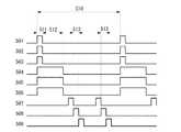
図4において、信号301〜信号307は、図1または図3におけるフォトダイオードリセット信号線210、ゲート信号線209、ゲート信号線211、ゲート信号線215、フォトセンサ出力信号線214、プリチャージ信号線217、バックゲート信号線218の電位に相当する。なお、フォトセンサ基準信号線213は低電位に設定されているものとする。4, signals 301 to 307 are the photodiode
また、図4に示すタイミングチャートは、リセット動作を行うリセット期間、電荷の累積動作を行う累積期間、読み出し動作を行う読み出し期間を有する。時刻Aから時刻Bまでの期間がリセット期間に相当する。時刻Bから時刻Cまでの期間が累積期間に相当する。時刻Dから時刻Eまでの期間が第1の読み出し期間、時刻Gから時刻Hまでの期間が第2の読み出し期間に相当する。4 includes a reset period in which a reset operation is performed, an accumulation period in which a charge accumulation operation is performed, and a read period in which a read operation is performed. A period from time A to time B corresponds to a reset period. A period from time B to time C corresponds to an accumulation period. The period from time D to time E corresponds to the first readout period, and the period from time G to time H corresponds to the second readout period.
以下では、高電位を”H”、低電位を”L”と表す。また以下では、トランジスタのゲートに高電位(”H”)の信号が供給された場合にトランジスタが導通状態となる例を示す。また以下では、トランジスタ205は、バックゲートの電位を高(低)くすることで、しきい値電圧が低(高)くなるトランジスタとして説明する。Hereinafter, the high potential is represented as “H” and the low potential is represented as “L”. In the following, an example in which a transistor is turned on when a high potential (“H”) signal is supplied to the gate of the transistor is described. In the following description, the
時刻Aにおいて、フォトダイオードリセット信号線210の電位(信号301)を”H”、ゲート信号線209の電位(信号302)を”H”とする(リセット動作開始)と、フォトダイオード204、トランジスタ207が導通状態となり、ゲート信号線215の電位(信号304)が”H”となる。すなわちゲート信号線215には高電位(”H”)に対応する電荷が蓄積される。At time A, when the potential of the photodiode reset signal line 210 (signal 301) is set to “H” and the potential of the gate signal line 209 (signal 302) is set to “H” (reset operation starts), the
また、プリチャージ信号線217の電位(信号306)を”H”とすると、フォトセンサ出力信号線214の電位(信号305)は”H”にプリチャージされる。バックゲート信号線218の電位(信号307)は0Vとし、この時、トランジスタ205のしきい値電圧が0V付近であるとする。When the potential of the precharge signal line 217 (signal 306) is set to “H”, the potential of the photosensor output signal line 214 (signal 305) is precharged to “H”. It is assumed that the potential of the back gate signal line 218 (signal 307) is 0 V and the threshold voltage of the
時刻Bにおいて、フォトダイオードリセット信号線210の電位(信号301)を”L”とし、ゲート信号線209の電位(信号302)を”H”のままとする(リセット動作終了、累積動作開始)と、フォトダイオード204のリーク電流により、ゲート信号線215の電位(信号304)が低下し始める。フォトダイオード204は、光が照射されるとリーク電流(光電流ともいう)が増大するので、照射される光(具体的には被検出物で反射された光)の強度に応じてゲート信号線215の電位(信号304)は変化する。すなわち、フォトダイオード204で生成された光電流により、ゲート信号線215の電荷量が変化する。これにより、トランジスタ205のゲートに蓄積された電荷量が変化し、トランジスタ205のソースとドレイン間のチャネル抵抗が変化する。このフォトダイオード204で生成された光電流を電気信号とみると、フォトダイオード204で生成された電気信号により、ゲート信号線215の電荷量が変化することになる。At time B, the potential of the photodiode reset signal line 210 (signal 301) is set to “L”, and the potential of the gate signal line 209 (signal 302) is set to “H” (reset operation end, cumulative operation start). The potential of the gate signal line 215 (signal 304) starts to decrease due to the leakage current of the
時刻Cにおいて、ゲート信号線209の電位(信号302)を”L”とする(累積動作終了)と、トランジスタ207は非導通状態となり、ゲート信号線215の電位(信号304)は一定となる。すなわち、ゲート信号線215に蓄積(累積)された電荷量が一定となり、トランジスタ205のゲートに蓄積(累積)された電荷量が一定となる。当該ゲート信号線215の電位(電荷量)は、累積動作中にフォトダイオードから生成された光電流の大きさにより決まる。すなわち、当該ゲート信号線215の電位(電荷量)は、フォトダイオードに照射されていた光の強度に応じて変化する。At the time C, when the potential of the gate signal line 209 (signal 302) is set to “L” (accumulation operation ends), the
トランジスタ207は、チャネル形成領域に酸化膜半導体層を用いたオフ電流が極めて低いトランジスタで構成する。そのため、後の読み出し動作を行うまで、上記電荷量を一定に保つことが可能である。このようにトランジスタ207は、トランジスタ205のゲートに電荷を蓄積(累積)する累積動作を制御する機能を有する。The
なお、ゲート信号線209の電位(信号302)を”L”とする際に、ゲート信号線209とゲート信号線215との間における寄生容量により、ゲート信号線215の電位(電荷量)が変化する。上記寄生容量による電位(電荷量)の変化量が大きい場合は、読み出しが正確に行えないことになる。上記寄生容量による電位(電荷量)の変化量を低減するには、トランジスタ207のゲート−ソース(もしくはゲート−ドレイン)間容量を低減する、トランジスタ205のゲート容量を増大する、ゲート信号線215に保持容量を設ける、などの対策が有効である。なお、図4では、これらの対策を施し、上記寄生容量による電位(電荷量)の変化を無視できるとしている。Note that when the potential of the gate signal line 209 (signal 302) is set to “L”, the potential (charge amount) of the
トランジスタ205は、ゲート信号線215の電位(信号304)に応じて導通状態または非導通状態となる。フォトダイオード204に照射されていた光の強度が低い場合は、ゲート信号線215の電位(信号304)が”H”から低下する割合が小さくなる。したがって、トランジスタ205は導通状態となり、ソースとドレイン間のチャネル抵抗も小さくなる。逆に、フォトダイオード204に照射されていた光の強度が高い場合は、ゲート信号線215の電位(信号304)が”H”から低下する割合が大きくなる。したがって、トランジスタ205は非導通状態となるか、或いは導通状態であってもソースとドレイン間のチャネル抵抗が大きくなる。ここでは累積動作後(時刻C)おけるゲート信号線215の電位(信号304)はトランジスタ205が導通状態となる値であると仮定する。The
時刻Dに、ゲート信号線211の電位(信号303)を”H”にする(第1の読み出し動作開始)と、トランジスタ206が導通状態となり、フォトセンサ基準信号線213とフォトセンサ出力信号線214とが、トランジスタ205とトランジスタ206とを介して導通する。フォトセンサ基準信号線213は低電位であるため、フォトセンサ出力信号線214の電位(信号305)は、低下していく。なお、時刻D以前に、プリチャージ信号線217の電位(信号306)は”L”とし、フォトセンサ出力信号線214のプリチャージを終了しておく。ここで、フォトセンサ出力信号線214の電位(信号305)が低下する速さは、トランジスタ205のソースとドレイン間のチャネル抵抗に依存する。すなわち、累積動作中にフォトダイオード204に照射されている光の強度に応じて変化する。At time D, when the potential of the gate signal line 211 (signal 303) is set to “H” (first reading operation starts), the
時刻Eにおいて、ゲート信号線211の電位(信号303)を”L”にする(第1の読み出し動作終了)と、トランジスタ206が非導通状態となり、フォトセンサ出力信号線214の電位(信号305)は、一定値となる。ここで、フォトセンサ出力信号線214の電位は、フォトダイオード204に照射されている光の強度によって決まる。したがって、フォトセンサ出力信号線214の電位を取得することで、累積動作中にフォトダイオード204に照射されていた光の強度を知ることができる。At time E, when the potential of the gate signal line 211 (signal 303) is set to “L” (first read operation ends), the
さて、フォトダイオード204に照射されていた光の強度が低い場合、トランジスタ205は導通状態となりソースとドレイン間のチャネル抵抗が小さくなる。そのため、フォトセンサ出力信号線214の電位(信号305)は”H”から低下する割合が大きく、フォトセンサ基準信号線213の電位とほとんど変わらない値になる。この場合、これ以下の弱い光と識別できないことになる。したがって、これより弱い光を識別するためには、フォトセンサ基準信号線213の電位とプリチャージ時のフォトセンサ出力信号線214の基準電位との電圧範囲を拡大することでも可能であるが、広電圧範囲に対応したA/D変換回路が必要になり、半導体装置または表示装置の製造コストが増大する。そこで、以下のような駆動方法を用いる。When the intensity of light applied to the
時刻F以前にバックゲート信号線218の電位(信号307)を負電位とする。この時、トランジスタ205のしきい値電圧は、0Vより高くなる。時刻Fにおいて、プリチャージ信号線217の電位(信号306)を”H”とし、フォトセンサ出力信号線214の電位(信号305)を”H”にプリチャージする。Prior to time F, the potential of the back gate signal line 218 (signal 307) is set to a negative potential. At this time, the threshold voltage of the
時刻Gにおいて、ゲート信号線211の電位(信号303)を”H”にする(第2の読み出し動作開始)と、トランジスタ206が導通状態となり、フォトセンサ基準信号線213とフォトセンサ出力信号線214とが、トランジスタ205とトランジスタ206とを介して導通する。すると、フォトセンサ出力信号線214の電位(信号305)は、低下していく。なお、時刻G以前に、プリチャージ信号線217の電位(信号306)は”L”とし、フォトセンサ出力信号線214のプリチャージを終了しておく。ここで、フォトセンサ出力信号線214の電位(信号305)が低下する速さは、トランジスタ205のソースとドレイン間のチャネル抵抗に依存する。すなわち、累積動作中にフォトダイオード204に照射されている光の強度に応じて変化する。しかし、第1の読み出し動作の際と比べ、トランジスタ205のしきい値電圧が高いため、フォトセンサ出力信号線214の電位(信号305)が低下する速さは緩やかになる。At time G, when the potential of the gate signal line 211 (signal 303) is set to “H” (second read operation starts), the
時刻Hにおいて、ゲート信号線211の電位(信号303)を”L”にする(第2の読み出し動作終了)と、トランジスタ206が非導通状態となり、フォトセンサ出力信号線214の電位(信号305)は、一定値となる。ここで、フォトセンサ出力信号線214の電位は、フォトダイオード204に照射されている光の強度によって決まる。したがって、フォトセンサ出力信号線214の電位を取得することで、累積動作中にフォトダイオード204に照射されていた光の強度を知ることができる。このようにして、光の強度が低い場合でも、より安価なA/D変換回路を用いて、フォトダイオード204に照射されていた光の強度を識別することが可能となる。At time H, when the potential of the gate signal line 211 (signal 303) is set to “L” (end of the second reading operation), the
上記は、フォトダイオードに照射する光の強度が低い(すなわち光が弱い)場合について説明したが、同様に、フォトダイオードに照射する光の強度が高い(すなわち光が強い)場合についても応用することができる。光が強い場合には、フォトセンサ出力信号線214の電位は、プリチャージ時の基準電位と概ね同一になり、識別が困難になる。そこで、第3の読み出し動作として、バックゲート信号線218の電位を正電位とし、トランジスタ205のしきい値電圧を0Vより低くしておく。これにより、フォトセンサ出力信号線214の電位(信号305)が低下する速さは向上し、フォトセンサ出力信号線214の電位の検出が容易になる。The above describes the case where the intensity of the light irradiating the photodiode is low (that is, the light is weak). Similarly, the case where the intensity of the light irradiating the photodiode is high (that is, the light is strong) is also applied. Can do. When the light is strong, the potential of the photosensor
また、フォトダイオードに照射する光が強い場合と、弱い場合と、の両方に対応するため、上記第1の読み出し動作〜第3の読み出し動作を繰り返して行うことが有効である。すなわち、第1のトランジスタのバックゲートの電位を第1の電位(ここでは0V)に設定し、第1のトランジスタのゲートに蓄積された電荷を第1の出力信号に変換し読み出す。次に、第1のトランジスタのバックゲートの電位を第2の電位(ここでは負電位)に設定し、第1のトランジスタのゲートに蓄積された電荷を第2の出力信号に変換し読み出す。次に、第1のトランジスタのバックゲートの電位を第3の電位(ここでは正電位)に設定し、第1のトランジスタのゲートに蓄積された電荷を第3の出力信号に変換し読み出す。また、第2の読み出し動作および第3の読み出し動作の際の、バックゲート信号線218の電位を、より細かい電圧幅で変更し、順次読み出しを行うことで、より広い範囲の光強度に対して、高い分解能で検出を行うことができる。すなわち、上記構成により、強い光や弱い光に対しても光を正確に電気信号に変換することができ、広範囲の光強度に応じた電気信号を出力することができるフォトセンサ106を提供することができる。In addition, it is effective to repeat the first to third reading operations in order to cope with both cases where the light applied to the photodiode is strong and weak. That is, the potential of the back gate of the first transistor is set to the first potential (here, 0 V), and the charge accumulated in the gate of the first transistor is converted into a first output signal and read. Next, the potential of the back gate of the first transistor is set to a second potential (here, a negative potential), and the charge accumulated in the gate of the first transistor is converted into a second output signal and read. Next, the potential of the back gate of the first transistor is set to a third potential (here, positive potential), and the charge accumulated in the gate of the first transistor is converted into a third output signal and read. In addition, by changing the potential of the back
以上のような駆動方法を実現するためには、累積動作が終了した後も、各フォトセンサにおけるゲート信号線215の電位が一定値を保つ必要がある。したがって、図1または図3で説明したように、トランジスタ207を、酸化物半導体層を用いて形成し、オフ電流が極めて低いトランジスタとする構成が有効である。In order to realize the driving method as described above, the potential of the
上記のように、個々のフォトセンサの動作は、リセット動作、累積動作、読み出し動作を繰り返すことで実現される。当該駆動方法を全画素について行うことで、撮像を行うことができる。より具体的には、行ごとにリセット動作、累積動作、読み出し動作を繰り返すことで実現される。As described above, the operation of each photosensor is realized by repeating the reset operation, the accumulation operation, and the readout operation. Imaging can be performed by performing the driving method for all the pixels. More specifically, this is realized by repeating the reset operation, the accumulation operation, and the read operation for each row.
本実施の形態によれば、広範囲の光強度に対して高分解能での撮像機能を実現できる安価な半導体装置または表示装置を提供することができる。According to the present embodiment, it is possible to provide an inexpensive semiconductor device or display device that can realize an imaging function with high resolution over a wide range of light intensities.
本実施の形態は、他の実施の形態、実施例と適宜組み合わせて実施することが可能である。This embodiment can be implemented in combination with any of the other embodiments and examples as appropriate.
(実施の形態4)
本実施の形態では、複数のフォトセンサを有する半導体装置の駆動方法の一例について説明する。(Embodiment 4)
In this embodiment, an example of a method for driving a semiconductor device including a plurality of photosensors will be described.
まず、図5に示すタイミングチャートのような駆動方法を考える。図5において、信号801、信号802、信号803は、各々第1行、第2行、第3行のフォトセンサにおけるフォトダイオードリセット信号線210に対応する。また、信号804、信号805、信号806は、各々第1行、第2行、第3行のフォトセンサにおけるゲート信号線209に対応する。また、信号807、信号808、信号809は、各々第1行、第2行、第3行のフォトセンサにおけるゲート信号線211に対応する。期間810は、1回の撮像を行う期間である。また、期間811、期間812、期間813は、第2行のフォトセンサが、各々リセット動作、累積動作、読み出し動作を行っている期間である。このように、異なる行のフォトセンサを順に駆動していくことで、撮像が可能になる。First, consider a driving method like the timing chart shown in FIG. In FIG. 5, a
ここで、累積動作は、行が異なると時間的にズレることがわかる。すなわち、全ての行のフォトセンサの撮像の同時性が損なわれる。そのため、撮像画像にブレが生じることになる。特に、第1行から第3行の方向に高速に移動する被検出物に対しては、尾を引くように、拡大されたような形状の撮像画像になり、逆方向に移動する被検出物に対しては、縮小されたような形状の撮像画像になるなど、形状が歪みやすい。Here, it can be seen that the cumulative operation is shifted in time when the rows are different. In other words, the simultaneous imaging of the photosensors in all rows is impaired. Therefore, the captured image is blurred. In particular, for a detection object that moves at high speed in the direction from the first row to the third row, the detection object that has a captured image with an enlarged shape so as to draw a tail and moves in the opposite direction On the other hand, the shape tends to be distorted, such as a captured image having a reduced shape.
異なる行のフォトセンサ間で累積動作に時間的なズレを生じさせないためには、異なる行のフォトセンサを駆動する間隔を短くすることが有効である。しかしながら、この場合、フォトセンサの出力信号をOPアンプもしくはA/D変換回路で非常に高速度で取得する必要がある。したがって、消費電力の増大を招く。特に、高解像度の画像を取得する場合には、非常に困難となる。In order not to cause a time shift in the cumulative operation between the photosensors in different rows, it is effective to shorten the interval for driving the photosensors in different rows. However, in this case, it is necessary to acquire the output signal of the photosensor with an OP amplifier or an A / D conversion circuit at a very high speed. Therefore, power consumption is increased. In particular, it is very difficult to acquire a high-resolution image.
そこで、図6に示すタイミングチャートのような駆動方法を提案する。図6において、信号501、信号502、信号503は、各々第1行、第2行、第3行のフォトセンサにおけるフォトダイオードリセット信号線210に対応する。また、信号504、信号505、信号506は、各々第1行、第2行、第3行のフォトセンサにおけるゲート信号線209に対応する。また、信号507、信号508、信号509は、各々第1行、第2行、第3行のフォトセンサにおけるゲート信号線211に対応する。期間510は、1回の撮像を行う期間である。また、期間511、期間512、期間513は、第2行のフォトセンサが、各々リセット動作(他の行でも共通)、累積動作(他の行でも共通)、読み出し動作を行っている期間である。Therefore, a driving method like the timing chart shown in FIG. 6 is proposed. In FIG. 6, a
図6において、図5と異なるのは、全行のフォトセンサについて、リセット動作と累積動作とが同時に行われ、累積動作終了後に累積動作とは非同期に、行ごとに順に読み出し動作を行う点である。累積動作を同時に行うことで、全ての行のフォトセンサにおける撮像の同時性が確保され、高速に移動する被検出物に対しても、ブレが少ない画像を容易に得ることができる。累積動作を同時に行うことで、複数のフォトセンサのフォトダイオードリセット信号線210の駆動回路を共通にすることができる。また、複数のフォトセンサのゲート信号線209の駆動回路も共通にすることができる。このように駆動回路を共通にすることは、周辺回路の削減や低消費電力化に有効である。さらに、読み出し動作を行ごとに順次行うことで、フォトセンサの出力信号を取得する際に、OPアンプもしくはA/D変換回路の動作速度を遅くすることが可能である。読み出し動作に要する合計の時間を、累積動作に要する時間より長くすることが好ましい。特に、高解像度の画像を取得する場合には、非常に有効である。6 differs from FIG. 5 in that the reset operation and the accumulation operation are simultaneously performed for the photosensors of all rows, and the read operation is sequentially performed for each row asynchronously with the accumulation operation after the accumulation operation is completed. is there. By performing the cumulative operation at the same time, the simultaneous imaging of the photosensors in all the rows is ensured, and an image with less blur can be easily obtained even for a detection object that moves at high speed. By simultaneously performing the accumulation operation, the drive circuit for the photodiode
上記図5、図6に示すタイミングチャートでは、1回の撮像を行う期間810および510において、読み出し動作を行う期間813および513を複数回有している。図5、図6では期間813および513を2回有しているが、光が強い場合と弱い場合との両方に対応するため、期間810および510において、読み出し動作を行う期間813および513を3回またはそれ以上有することが有効である。複数回の読み出し動作は、図5、図6に示すタイミングチャートのように、まず全ての行において第1の読み出し動作を行ごとに行い、その後、全ての行において第2の読み出し動作を行ごとに行い、この動作を繰り返して第nの読み出し動作(nは3以上の整数)まで行う。または、まず第1行において第1の読み出し動作〜第nの読み出し動作を行い、その後、第2行において第1の読み出し動作〜第nの読み出し動作を行い、この動作を繰り返して第m行(mは3以上の整数)まで行う。In the timing charts shown in FIGS. 5 and 6, the
なお、図5、図6では、フォトセンサを行ごとに順次駆動する駆動方法のタイミングチャートを示したが、特定の領域における画像を取得するために、特定の行におけるフォトセンサのみを順次駆動する駆動方法も有効である。これにより、OPアンプもしくはA/D変換回路の動作を軽減し、消費電力を低減しながら、必要な画像を取得することができる。Note that FIGS. 5 and 6 show timing charts of a driving method in which the photosensors are sequentially driven for each row. However, in order to acquire an image in a specific region, only the photosensors in the specific row are sequentially driven. The driving method is also effective. Thereby, the operation of the OP amplifier or the A / D conversion circuit can be reduced, and a necessary image can be acquired while reducing power consumption.
以上のような駆動方法を実現するためには、累積動作が終了した後も、各フォトセンサにおけるゲート信号線215の電位を一定に保つ必要がある。したがって、図1または図3で説明したように、トランジスタ207は、酸化物半導体を用いて形成され、オフ電流が極めて小さいことが好ましい。In order to realize the above driving method, it is necessary to keep the potential of the
以上のような形態とすることで、高速で移動する被検出物に対してもブレが少なく、高解像度の撮像が実現でき、且つ低消費電力の表示装置又は半導体装置を提供することができる。With the above configuration, it is possible to provide a display device or a semiconductor device that has less blur even for an object that moves at high speed, can realize high-resolution imaging, and has low power consumption.
本実施の形態は、他の実施の形態、実施例と適宜組み合わせて実施することができる。This embodiment can be implemented in combination with any of the other embodiments and examples as appropriate.
(実施の形態5)
本実施の形態では、図1または図3におけるフォトセンサ106の回路構成の変形例について説明する。(Embodiment 5)
In this embodiment, a modification of the circuit configuration of the photosensor 106 in FIG. 1 or 3 will be described.
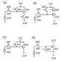
図7(A)は、図1または図3においてトランジスタ205のゲートに、フォトセンサのリセット動作を制御するためのトランジスタ601を接続した構成を示している。具体的には、トランジスタ601のソース又はドレインの一方がフォトセンサ基準信号線213に電気的に接続され、他方がトランジスタ205のゲートに電気的に接続されている。また、フォトダイオード204の一方の電極は所定の電位(例えばグランド電位)を供給する配線に電気的に接続されている。FIG. 7A illustrates a structure in which the
トランジスタ601は、非晶質半導体、微結晶半導体、多結晶半導体、酸化物半導体、又は単結晶半導体などを用いることが可能である。特に、リセット動作終了後にトランジスタ205のゲートの電荷がトランジスタ601から放出することを防止するため、酸化物半導体を用い、オフ電流の小さいトランジスタとすることが望ましい。The
図7(B)は、図7(A)においてトランジスタ205とトランジスタ206との接続関係を逆にした構成を示している。具体的には、トランジスタ205のソース又はドレインの一方がフォトセンサ出力信号線214に電気的に接続され、トランジスタ206のソース又はドレインの一方が、フォトセンサ基準信号線213に電気的に接続されている。FIG. 7B illustrates a structure in which the connection relation between the
図7(C)は、図7(A)においてトランジスタ206を省略した構成を示す。具体的には、トランジスタ205のソース又はドレインの一方がフォトセンサ基準信号線213に電気的に接続され、他方がフォトセンサ出力信号線214に電気的に接続されている。FIG. 7C illustrates a structure in which the
なお、図7(A)〜(C)において、トランジスタ601のソース又はドレインの一方は、フォトセンサ基準信号線213とは異なる配線に電気的に接続されていてもよい。7A to 7C, one of the source and the drain of the
図7(D)は、図7(C)においてトランジスタ601のソース又はドレインの一方がフォトセンサ出力信号線214に電気的に接続され、他方がトランジスタ205のゲートに電気的に接続されている。In FIG. 7D, one of the source and the drain of the
図7(A)〜(D)において、トランジスタ207に酸化物半導体を用いることで、オフ電流が低減できるため、トランジスタ205のゲートに蓄積した電荷を一定に保つことが可能となる。7A to 7D, an off-state current can be reduced by using an oxide semiconductor for the
図7(A)〜(D)において、トランジスタ205にバックゲートを設けることで、広範囲の光強度に対して高分解能での撮像機能を実現できる半導体装置を提供することができる。7A to 7D, by providing the
図7において、フォトセンサの回路構成に応じて、フォトダイオード204の二つの電極の接続先を逆にしてもよい。In FIG. 7, the connection destination of the two electrodes of the
本実施の形態は、他の実施の形態、実施例と適宜組み合わせて実施することができる。This embodiment can be implemented in combination with any of the other embodiments and examples as appropriate.
(実施の形態6)
本実施の形態では、開示する発明の一態様である半導体装置が有するトランジスタの一例について説明する。具体的には、図1または図3に示したトランジスタ207、図3に示したトランジスタ201のようにチャネル形成領域が酸化物半導体層により形成されたトランジスタの一例について説明する。(Embodiment 6)
In this embodiment, an example of a transistor included in a semiconductor device which is one embodiment of the disclosed invention will be described. Specifically, an example of a transistor in which a channel formation region is formed using an oxide semiconductor layer like the
<トランジスタ>
トランジスタ(例えば図1または図3に示すトランジスタ207)は、チャネル形成領域が酸化物半導体層によって構成されるトランジスタである。該酸化物半導体層は、トランジスタの電気的特性の変動要因となる水素、水分、水酸基又は水素化物などのドナーとなりうる不純物が徹底的に取り除かれ、可能な限り含まれる不純物の濃度が小さくされ、かつ不純物を排除するステップによって同時に減少してしまう酸化物半導体の主成分材料である酸素が供給されることによって、高純度化され、電気的にI型(真性)或いは実質的にI型(真性)化された酸化物半導体層である。なお、当該酸化物半導体層を構成する酸化物半導体は3.0eV以上のバンドギャップを有する。<Transistor>
A transistor (eg, the
また、高純度化された酸化物半導体中にはキャリアが極めて少なく(ゼロに近い)、キャリア密度は非常に小さい値(例えば、1×10¹²/cm3未満、望ましくは、1×1011/cm3未満)をとる。そして、これにより、トランジスタのオフ電流が非常に小さくなる。従って、上記したトランジスタにおいて、チャネル幅(w)が1μmあたりの室温におけるオフ電流値を1aA/μm(1×10−18A/μm)以下、さらには100zA/μm(1×10−19A/μm)未満にすることが可能である。なお、一般に、アモルファスシリコンを用いたトランジスタでは、室温におけるオフ電流値は1×10−13A/μm以上となる。さらに、上記したような、高純度化された酸化物半導体層を用いたトランジスタはホットキャリア劣化もないと考えられる。そのため、トランジスタの電気的特性はホットキャリア劣化の影響を受けない。In the highly purified oxide semiconductor, the number of carriers is extremely small (near zero), and the carrier density is very small (for example, less than 1 × 10¹² / cm3 , desirably 1 × 10¹¹ / cm <3 ). As a result, the off-state current of the transistor becomes very small. Therefore, in the above transistor, the channel current (w) has an off-current value at room temperature per 1 μm of 1 aA / μm (1 × 10⁻¹⁸ A / μm) or less, and further 100 zA / μm (1 × 10⁻¹⁹ A / μm). μm). Note that generally, in a transistor using amorphous silicon, an off-state current value at room temperature is 1 × 10⁻¹³ A / μm or more. Furthermore, it is considered that a transistor using a highly purified oxide semiconductor layer as described above does not have hot carrier deterioration. Therefore, the electrical characteristics of the transistor are not affected by hot carrier deterioration.
このように酸化物半導体層に含まれる水素を徹底的に除去することにより高純度化された酸化物半導体層をトランジスタのチャネル形成領域に用いたトランジスタは、オフ電流値を極めて低くすることができる。つまり、トランジスタがオフ状態(非導通状態ともいう)において、酸化物半導体層を絶縁体とみなして回路設計を行うことができる。一方で、酸化物半導体をトランジスタのチャネル形成領域に用いたトランジスタは、オン状態(導通状態ともいう)においては、アモルファスシリコンを用いたトランジスタよりも高い電流供給能力が見込まれている。As described above, a transistor in which a highly purified oxide semiconductor layer is used for a channel formation region of a transistor by thoroughly removing hydrogen contained in the oxide semiconductor layer can have an extremely low off-state current value. . That is, when the transistor is off (also referred to as a non-conduction state), the circuit can be designed with the oxide semiconductor layer regarded as an insulator. On the other hand, a transistor using an oxide semiconductor for a channel formation region of a transistor is expected to have higher current supply capability in an on state (also referred to as a conductive state) than a transistor using amorphous silicon.
また、低温ポリシリコンを用いたトランジスタでは、酸化物半導体を用いたトランジスタと比べて、室温におけるオフ電流値が10000倍程度大きい値であると見積もられている。そのため、酸化物半導体を用いたトランジスタでは、低温ポリシリコンを用いたトランジスタに比べて電荷の保持期間を10000倍程度に引き延ばすことができる。In addition, in a transistor using low-temperature polysilicon, an off-state current value at room temperature is estimated to be about 10,000 times larger than that of a transistor using an oxide semiconductor. Therefore, in a transistor using an oxide semiconductor, a charge holding period can be extended by about 10,000 times compared to a transistor using low-temperature polysilicon.
上記のとおり、高純度化された酸化物半導体層をトランジスタのチャネル形成領域に用いたトランジスタは、トランジスタのソース又はドレインのいずれかに蓄積された電荷を長期間保持することが可能となる。As described above, a transistor in which a purified oxide semiconductor layer is used for a channel formation region of the transistor can hold charge accumulated in either the source or the drain of the transistor for a long time.
したがって、図1または図3に示すトランジスタ207のチャネル形成領域に酸化物半導体層を用いることにより、図1または図3に示すトランジスタ205のゲートに蓄積された電荷を長期間保持することが可能となる。これにより、トランジスタ205のゲートに蓄積された電荷の読み出しを複数回行う間において、トランジスタ205のゲートに蓄積された電荷をほぼ一定に保持することが可能となる。すなわち、トランジスタ207のチャネル形成領域に酸化物半導体層を用いることにより、新規な回路構成を有するフォトセンサを有する半導体装置を提供することができる。Therefore, by using an oxide semiconductor layer in the channel formation region of the
また、図3に示すトランジスタ201のチャネル形成領域に酸化物半導体層を用いることにより、画素の画像信号の保持期間を長くすることができる。そのため、画素に設けられる容量素子のサイズを縮小することが可能になる。これにより、当該画素の開口率を向上させることおよび当該画素への画像信号の入力を高速に行うことなどが可能になる。また、静止画を表示する際の画像信号の再書き込みの間隔を長くすることができる。例えば、画像信号の書き込みの間隔を10秒以上、30秒以上、あるいは1分以上とすることができる。書き込みの間隔を長くすることにより、それだけ消費電力を抑えることができる。In addition, when an oxide semiconductor layer is used for a channel formation region of the
なお、本明細書では、キャリア濃度が1×10¹¹/cm3未満の半導体を「真性」あるいは「I型」、キャリア濃度がそれ以上であるが、1×1012/cm3未満のものを、「実質的に真性」あるいは「実質的にI型」という。In this specification, a semiconductor having a carrier concentration of less than 1 × 10¹¹ / cm3 is “intrinsic” or “I-type”, and a carrier concentration is higher than that, but less than 1 × 10¹² / cm3. , “Substantially intrinsic” or “substantially type I”.
<トランジスタの作製方法>
チャネル形成領域が酸化物半導体層により形成されたトランジスタの作製方法の一例について、図8を参照して説明する。<Method for Manufacturing Transistor>
An example of a method for manufacturing a transistor in which a channel formation region is formed using an oxide semiconductor layer will be described with reference to FIGS.
図8(A)〜(D)は、チャネル形成領域が酸化物半導体層により形成されたトランジスタの構成および作製工程の一例を示す断面図である。図8(D)に示すトランジスタ410は、ボトムゲート型の一つである逆スタガ型構造を有している。また、チャネルエッチ型構造を有している。また、シングルゲート構造を有している。8A to 8D are cross-sectional views illustrating an example of a structure and a manufacturing process of a transistor in which a channel formation region is formed using an oxide semiconductor layer. A
しかし、トランジスタの構造はこれに限定されずトップゲート型構造を有していてもよい。また、チャネルストップ型構造を有していてもよい。また、マルチゲート構造を有していてもよい。However, the structure of the transistor is not limited to this and may have a top-gate structure. Further, it may have a channel stop type structure. Moreover, you may have a multi-gate structure.
以下、図8(A)〜(D)を参照して、基板400上にトランジスタ410を作製する工程について説明する。Hereinafter, a process for manufacturing the
まず、絶縁表面を有する基板400上にゲート電極層411を形成する(図8(A)参照)。First, the
絶縁表面を有する基板400として使用することができる基板に大きな制限はないが、少なくとも、後の加熱処理に耐えうる程度の耐熱性を有していることが必要となる。例えば、絶縁表面を有する基板400としてガラス基板を用いることができる。また、絶縁表面を有する基板400としてガラス基板又は単結晶基板上に素子が形成された素子基板を用いることができる。素子基板を用いる場合は、その表面に絶縁層を有する構成とすることができる。There is no particular limitation on a substrate that can be used as the
基板400とゲート電極層411との間には、下地膜となる絶縁膜を設けてもよい。下地膜は、基板400からの不純物元素の拡散を防止する機能があり、窒化シリコン膜、酸化シリコン膜、窒化酸化シリコン膜、又は酸化窒化シリコン膜から選ばれた一又は複数の膜による積層構造により形成することができる。ここでは、プラズマCVD法を用いて窒化シリコン膜を100nmの厚さとなるように形成し、窒化シリコン膜上にプラズマCVD法を用いて酸化窒化シリコン膜(SiON膜)を150nmの厚さとなるように形成した。An insulating film serving as a base film may be provided between the
なお、下地膜は、できるだけ、水素や水などの不純物を含まないように形成することが好ましい。Note that the base film is preferably formed so as not to contain impurities such as hydrogen and water as much as possible.
ゲート電極層411は、基板400上に導電層を形成し、第1のフォトリソグラフィ工程により該導電層を選択的にエッチングすることで形成することができる。The
ゲート電極層411の材料は、モリブデン、チタン、クロム、タンタル、タングステン、アルミニウム、銅、ネオジム、スカンジウム等の金属又はこれらを主成分とする合金又はこれらの金属元素を主成分とする窒化物材料を用いて、単層で又は積層して形成することができる。ここでは、スパッタ法を用いてタングステン膜を100nmの厚さとなるように形成し、タングステン膜をエッチングしてゲート電極層411とした。The material of the
次いで、ゲート電極層411上にゲート絶縁層402を形成する(図8(A)参照)。Next, the
ゲート絶縁層402は、プラズマCVD法又はスパッタ法等を用いて、酸化シリコン層、窒化シリコン層、酸化窒化シリコン層、窒化酸化シリコン層、若しくは酸化アルミニウム層を単層で又は積層して形成することができる。例えば、成膜ガスとして、シラン(SiH4)、酸素および窒素を用いてプラズマCVD法により酸化窒化シリコン層を形成すればよい。また、ゲート絶縁層として酸化ハフニウム(HfOx)、酸化タンタル(TaOx)等のHigh−k材料を用いることもできる。ゲート絶縁層402の厚さは、例えば、10nm以上500nm以下とすることができる。The
ここでは、ゲート電極層411上にマイクロ波(例えば、周波数2.45GHz)を用いた高密度プラズマCVD法を用いて、酸化窒化シリコン膜を100nmの厚さとなるように形成してゲート絶縁層とした。マイクロ波を用いた高密度プラズマCVD法は、緻密で絶縁耐圧の高い高品質なゲート絶縁層402を形成できる点で好適である。また、酸化物半導体層と高品質なゲート絶縁層402とが密接することにより、界面準位を低減して界面特性を良好なものとすることができる。Here, a silicon oxynitride film having a thickness of 100 nm is formed over the
なお、ゲート絶縁層402は、可能な限り、水素や水などの不純物が含まれないように形成することが好ましい。すなわち、ゲート絶縁層402は、含まれる水素や水などの不純物の濃度が可能な限り小さくなるように形成することが好ましい。Note that the
次に、ゲート絶縁層402上に酸化物半導体膜430を形成する(図8(A)参照)。酸化物半導体膜430は、スパッタ法を用いて形成することができる。酸化物半導体膜430の厚さは、2nm以上200nm以下とすることができる。Next, the
なお、酸化物半導体膜430をスパッタ法により成膜する前に、アルゴンガスを導入してプラズマを発生させる逆スパッタを行うことが好ましい。逆スパッタを行うことにより、ゲート絶縁層402の表面に付着している粉状物質(パーティクル、ゴミともいう)を除去することができる。逆スパッタとは、ターゲット側に電圧を印加せずに、基板側にRF電源を用いて電圧を印加してプラズマを形成し、基板表面を改質する方法である。なお、アルゴン雰囲気に代えて窒素、ヘリウム、酸素などを用いてもよい。Note that before the
酸化物半導体膜430は、In−Ga−Zn−O系、In−Sn−O系、In−Sn−Zn−O系、In−Al−Zn−O系、Sn−Ga−Zn−O系、Al−Ga−Zn−O系、Sn−Al−Zn−O系、In−Zn−O系、Sn−Zn−O系、Al−Zn−O系、In−O系、Sn−O系、Zn−O系の材料を用いることができる。また、上記材料にSiO2を含ませても良い。The
酸化物半導体膜430は、希ガス(代表的にはアルゴン)雰囲気下、酸素雰囲気下、又は希ガス(代表的にはアルゴン)および酸素の混合雰囲気下においてスパッタ法により形成することができる。The
ここでは、In、GaおよびZnを含むIn−Ga−Zn−O系の金属酸化物ターゲットを用いて、スパッタ法により酸化物半導体層を30nmの厚さとなるように形成した。なお、スパッタガスはAr/O2とし、基板温度は200℃とした。Here, an oxide semiconductor layer was formed to a thickness of 30 nm by a sputtering method using an In—Ga—Zn—O-based metal oxide target containing In, Ga, and Zn. The sputtering gas was Ar / O2 and the substrate temperature was 200 ° C.
なお、酸化物半導体膜430は、可能な限り、水素や水などの不純物が含まれないように形成することが好ましい。すなわち、酸化物半導体膜430は、含まれる水素や水などの不純物の濃度が可能な限り小さくなるように形成することが好ましい。Note that the
次に、酸化物半導体膜430を第2のフォトリソグラフィ工程により選択的にエッチングして島状の酸化物半導体層431を形成する(図8(B)参照)。酸化物半導体膜430のエッチングは、ウェットエッチングを用いて行うことができる。しかしこれに限定されずドライエッチングを用いてもよい。Next, the
次いで、酸化物半導体層431に対して第1の熱処理を行う。この第1の熱処理によって酸化物半導体層431中の過剰な水や水素などを除去することができる。第1の熱処理の温度は、350℃以上基板の歪み点未満、好ましくは400℃以上基板の歪み点未満とすることができる。Next, first heat treatment is performed on the
第1の熱処理の温度を350℃以上とすることにより酸化物半導体層の脱水化または脱水素化が行え、膜中の水素濃度を低減することができる。また第1の熱処理の温度を450℃以上とすることにより、膜中の水素濃度をさらに低減することができる。また第1の熱処理の温度を550℃以上とすることにより、膜中の水素濃度をさらに低減することができる。By setting the temperature of the first heat treatment to 350 ° C. or higher, the oxide semiconductor layer can be dehydrated or dehydrogenated, and the hydrogen concentration in the film can be reduced. In addition, by setting the temperature of the first heat treatment to 450 ° C. or higher, the hydrogen concentration in the film can be further reduced. In addition, by setting the temperature of the first heat treatment to 550 ° C. or higher, the hydrogen concentration in the film can be further reduced.
第1の熱処理を行う雰囲気としては、窒素、または希ガス(ヘリウム、ネオン、アルゴン等)を主成分とする不活性気体であって、水、水素などが含まれない気体を用いるのが望ましい。例えば、熱処理装置に導入する気体の純度を6N(99.9999%)以上、好ましくは7N(99.99999%)以上とすることができる。これにより、第1の熱処理の間、酸化物半導体層431は、大気に触れることなく、水や水素の再混入が行われないようにすることができる。As an atmosphere in which the first heat treatment is performed, it is desirable to use an inert gas containing nitrogen or a rare gas (such as helium, neon, or argon) as a main component and not containing water, hydrogen, or the like. For example, the purity of the gas introduced into the heat treatment apparatus can be 6N (99.9999%) or higher, preferably 7N (99.99999%) or higher. Thus, during the first heat treatment, the
なお、熱処理装置は電気炉に限られず、抵抗発熱体などの発熱体からの熱伝導または熱輻射によって、被処理物を加熱する装置を備えていてもよい。例えば、GRTA(Gas Rapid Thermal Anneal)装置、LRTA(Lamp Rapid Thermal Anneal)装置等のRTA(Rapid Thermal Anneal)装置を用いることができる。LRTA装置は、ハロゲンランプ、メタルハライドランプ、キセノンアークランプ、カーボンアークランプ、高圧ナトリウムランプ、高圧水銀ランプなどのランプから発する光(電磁波)の輻射により、被処理物を加熱する装置である。GRTA装置は、高温のガスを用いて熱処理を行う装置である。気体には、アルゴンなどの希ガスまたは窒素のような、加熱処理によって被処理物と反応しない不活性気体が用いられる。Note that the heat treatment apparatus is not limited to an electric furnace, and may include a device for heating an object to be processed by heat conduction or heat radiation from a heating element such as a resistance heating element. For example, a rapid thermal annealing (RTA) device such as a GRTA (Gas Rapid Thermal Anneal) device or an LRTA (Lamp Rapid Thermal Anneal) device can be used. The LRTA apparatus is an apparatus that heats an object to be processed by radiation of light (electromagnetic waves) emitted from a lamp such as a halogen lamp, a metal halide lamp, a xenon arc lamp, a carbon arc lamp, a high pressure sodium lamp, or a high pressure mercury lamp. The GRTA apparatus is an apparatus that performs heat treatment using a high-temperature gas. As the gas, an inert gas that does not react with an object to be processed by heat treatment, such as nitrogen or a rare gas such as argon, is used.
本実施の形態では、第1の熱処理として、GRTA装置を用い、窒素雰囲気で650℃、6分の熱処理を行った。In this embodiment, as the first heat treatment, heat treatment is performed at 650 ° C. for 6 minutes in a nitrogen atmosphere using a GRTA apparatus.
また、酸化物半導体層の第1の熱処理は、島状の酸化物半導体層に加工する前の酸化物半導体膜430に対して行うこともできる。その場合には、第1の熱処理後に第2のフォトリソグラフィ工程を行う。The first heat treatment of the oxide semiconductor layer can be performed on the
その後、ゲート絶縁層402および酸化物半導体層431を覆うように導電層を形成し、第3のフォトリソグラフィ工程により該導電層をエッチングすることで、ソース電極層およびドレイン電極層415a、415bを形成する(図8(C)参照)。After that, a conductive layer is formed so as to cover the
導電層の材料は、アルミニウム、クロム、銅、タンタル、チタン、モリブデン、タングステンから選ばれた金属や、上記金属元素を成分とする窒化物や、上記金属を成分とする合金等を用いることができる。マンガン、マグネシウム、ジルコニウム、ベリリウム、イットリウムから選ばれた材料を用いてもよい。また、アルミニウムに、チタン、タンタル、タングステン、モリブデン、クロム、ネオジム、スカンジウムから選ばれた金属を単数または複数種類含有させた材料を用いてもよい。As a material for the conductive layer, a metal selected from aluminum, chromium, copper, tantalum, titanium, molybdenum, and tungsten, a nitride including the above metal element, an alloy including the above metal, or the like can be used. . A material selected from manganese, magnesium, zirconium, beryllium, and yttrium may be used. Alternatively, a material in which one or more kinds of metals selected from titanium, tantalum, tungsten, molybdenum, chromium, neodymium, and scandium are contained in aluminum may be used.
また、導電層は、酸化物導電膜を用いて形成してもよい。酸化物導電膜としては、酸化インジウム(In2O3)、酸化スズ(SnO2)、酸化亜鉛(ZnO)、酸化インジウムと酸化スズ混合酸化物(In2O3―SnO2、ITOと略記する場合がある)、酸化インジウム酸化亜鉛の混合酸化物(In2O3―ZnO)、または、これらの酸化物導電材料にシリコン若しくは酸化シリコンを含有させたものを用いることができる。The conductive layer may be formed using an oxide conductive film. The oxide conductive film is abbreviated as indium oxide (In2 O3 ), tin oxide (SnO2 ), zinc oxide (ZnO), indium oxide and tin oxide mixed oxide (In2 O3 —SnO2 , ITO). In some cases, a mixed oxide of indium zinc oxide (In2 O3 —ZnO), or a conductive oxide containing these oxides containing silicon or silicon oxide can be used.
この場合には、酸化物導電膜の材料は、酸化物半導体層431に用いる材料と比較して、導電率が高いまたは抵抗率が低い材料を用いることが好ましい。酸化物導電膜の導電率は、キャリア濃度を増やすことで高くすることができる。酸化物導電膜のキャリア濃度は、水素濃度を増やすことや、酸素欠損を増やすことにより増やすことができる。In this case, it is preferable to use a material having a higher conductivity or a lower resistivity than the material used for the
ソース電極層およびドレイン電極層415a、415bは、単層構造としてもよいし、2層以上の積層構造としてもよい。The source and drain
本実施の形態では、酸化物半導体層431上に第1のチタン層を100nm、アルミニウム層を400nm、第2のチタン層を100nmの厚さとなるようにこの順で形成した。そして、第1のチタン層、アルミニウム層および第2のチタン層からなる積層膜をエッチングして、ソース電極層およびドレイン電極層415a、415bを形成した(図8(C)参照)。In this embodiment, the first titanium layer is formed with a thickness of 100 nm, the aluminum layer with a thickness of 400 nm, and the second titanium layer with a thickness of 100 nm over the
上記酸化物半導体層の第1の熱処理は、ソース電極層およびドレイン電極層を形成した後に行っても良い。ソース電極層およびドレイン電極層形成後に第1の熱処理を行う場合は、この熱処理に耐える耐熱性を有する導電層を選択する。The first heat treatment of the oxide semiconductor layer may be performed after the source electrode layer and the drain electrode layer are formed. In the case where the first heat treatment is performed after the source electrode layer and the drain electrode layer are formed, a conductive layer having heat resistance that can withstand the heat treatment is selected.
なお、導電層のエッチングの際に、酸化物半導体層431は除去されないようにそれぞれの材料およびエッチング条件を適宜調節する。Note that each material and etching conditions are adjusted as appropriate so that the
なお、第3のフォトリソグラフィ工程では、酸化物半導体層431は一部がエッチングされ、溝部(凹部)を有する酸化物半導体層となることもある。Note that in the third photolithography step, part of the
次に、亜酸化窒素(N2O)、窒素(N2)、またはアルゴン(Ar)などのガスを用いたプラズマ処理を行う。このプラズマ処理によって露出している酸化物半導体層の表面に付着した吸着水などを除去する。また、酸素とアルゴンの混合ガスを用いてプラズマ処理を行ってもよい。Next, plasma treatment using a gas such as nitrous oxide (N2 O), nitrogen (N2 ), or argon (Ar) is performed. Adsorbed water or the like attached to the surface of the oxide semiconductor layer exposed by this plasma treatment is removed. Further, plasma treatment may be performed using a mixed gas of oxygen and argon.
プラズマ処理を行った後、酸化物半導体層を大気に触れさせることなく、酸化物半導体層の一部に接する保護絶縁膜となる酸化物絶縁層416を形成する(図8(D)参照)。After the plasma treatment, the
酸化物絶縁層416は、スパッタ法など水素や水などの不純物が含まれない方法により形成することができる。酸化物絶縁層416の厚さは、少なくとも1nm以上とすることができる。酸化物絶縁層416に水素が含まれると、水素の酸化物半導体層431への侵入が生じ、酸化物半導体層431のバックチャネルが低抵抗化(N型化)してしまい、寄生チャネルが形成されるおそれがある。よって、酸化物絶縁層416はできるだけ水素を含まない膜になるように、成膜方法に水素を用いないことが重要である。The
酸化物絶縁層416の成膜時の基板温度は、室温以上300℃以下とすればよい。また、成膜雰囲気は、希ガス(代表的にはアルゴン)雰囲気、酸素雰囲気、または希ガス(代表的にはアルゴン)および酸素雰囲気とすることができる。The substrate temperature at the time of forming the
本実施の形態では、酸化物絶縁層416の形成前に200℃の温度で基板を加熱し、ソース電極層およびドレイン電極層415a、415bを覆うように、酸化物絶縁層416として酸化シリコン膜を300nmの厚さとなるように形成した。酸化シリコン膜は、シリコンターゲットを用い、酸素をスパッタガスとして用いたスパッタ法により形成した。In this embodiment, the substrate is heated at a temperature of 200 ° C. before the
次に、不活性ガス雰囲気下、または酸素ガス雰囲気下で第2の熱処理(好ましくは200℃以上400℃以下、例えば250℃以上350℃以下)を行う。例えば、窒素雰囲気下で250℃、1時間の第2の熱処理を行う。第2の熱処理を行うと、酸化物半導体層の一部(チャネル形成領域)が酸化物絶縁層416と接した状態で加熱される。第2の熱処理により、酸化物半導体層の一部(チャネル形成領域)に酸素が供給される。これにより、ゲート電極層411と重なるチャネル形成領域413をI型に近づけることができる。以上の工程でトランジスタ410が形成される。Next, second heat treatment (preferably 200 ° C. to 400 ° C., for example, 250 ° C. to 350 ° C.) is performed in an inert gas atmosphere or an oxygen gas atmosphere. For example, the second heat treatment is performed at 250 ° C. for 1 hour in a nitrogen atmosphere. When the second heat treatment is performed, part of the oxide semiconductor layer (a channel formation region) is heated in contact with the
酸化物絶縁層416上にさらに保護絶縁層403を形成してもよい(図8(D)参照)。例えば、RFスパッタ法を用いて窒化シリコン膜を形成することができる。RFスパッタ法は、量産性がよいため、保護絶縁層の成膜方法として好ましい。保護絶縁層は、水分や、水素イオンや、OH−などの不純物を含まず、これらが外部から侵入することをブロックする無機絶縁膜を用いることが好ましい。A protective insulating
さらに大気中、100℃以上200℃以下、1時間以上30時間以下での熱処理を行ってもよい。この加熱処理は一定の加熱温度を保持して加熱してもよいし、室温から、100℃以上200℃以下の所定の温度への昇温と、所定の温度から室温までの降温を複数回くりかえして行ってもよい。また、この熱処理を、酸化物絶縁膜の形成前に、減圧下で行ってもよい。減圧下で熱処理を行うことにより加熱時間を短縮することができる。この熱処理によって、酸化物半導体層431から酸化物絶縁層416中に水素をとりこむことができる。すなわち、さらに酸化物半導体層から水素を除去することができる。Further, heat treatment may be performed in the air at 100 ° C. or higher and 200 ° C. or lower for 1 hour or longer and 30 hours or shorter. This heat treatment may be performed while maintaining a constant heating temperature, or a temperature increase from a room temperature to a predetermined temperature of 100 ° C. to 200 ° C. and a temperature decrease from the predetermined temperature to the room temperature are repeated a plurality of times. You may go. Further, this heat treatment may be performed under reduced pressure before the formation of the oxide insulating film. Heating time can be shortened by performing heat treatment under reduced pressure. Through this heat treatment, hydrogen can be taken from the
このようにして得られるトランジスタ410に対し、例えば85℃、2×10⁶V/cm、12時間という条件のゲートバイアス・熱ストレス試験(BT試験)を行ってもトランジスタの電気的特性にほとんど変化はみられず、安定な電気的特性が得ることができる。Even when the
本実施の形態に示す酸化物半導体を用いたトランジスタは、シリコン等を用いたトランジスタと比べてオフ電流が非常に小さいという電気的特性を有する。The transistor including an oxide semiconductor described in this embodiment has electrical characteristics such that the off-state current is extremely small as compared with a transistor including silicon or the like.
したがって、図1または図3に示すトランジスタ207として本実施の形態に示すトランジスタを用いることにより、図1または図3に示すトランジスタ205のゲートに蓄積された電荷を長期間保持することが可能となる。これにより、トランジスタ205のゲートに蓄積された電荷の読み出しを複数回行う間において、トランジスタ205のゲートに蓄積された電荷をほぼ一定に保持することが可能となる。すなわち、トランジスタ207のチャネル形成領域に酸化物半導体層を用いることにより、新規な回路構成を有するフォトセンサを有する半導体装置を提供することができる。Therefore, by using the transistor described in this embodiment as the
また、図3に示すトランジスタ201として本実施の形態に示すトランジスタを用いることにより、画素の画像信号の保持期間を長くすることができる。そのため、画素に設けられる容量素子のサイズを縮小することが可能になる。これにより、当該画素の開口率を向上させることおよび当該画素への画像信号の入力を高速に行うことなどが可能になる。また、静止画を表示する際の画像信号の再書き込みの間隔を長くすることができる。例えば、画像信号の書き込みの間隔を10秒以上、30秒以上、あるいは1分以上10分未満とすることができる。書き込みの間隔を長くすることにより、それだけ消費電力を抑えることができる。In addition, when the transistor described in this embodiment is used as the
また、図1または図3に示すトランジスタ206として本実施の形態に示すトランジスタを用いることにより、他の画素の読み出し期間中に図3に示すフォトセンサ出力信号線214に不必要な電位が出力されることを防ぐことができる。In addition, by using the transistor described in this embodiment as the
また、図1または図3に示すトランジスタ205として本実施の形態に示すトランジスタにバックゲートを追加した構造を有するトランジスタを用いることができる。これにより、他の画素の読み出し期間中にフォトセンサ出力信号線214に不必要な電位が出力されることを防ぐことができる。1 or 3 can be a transistor having a structure in which a back gate is added to the transistor described in this embodiment. Accordingly, it is possible to prevent an unnecessary potential from being output to the photosensor
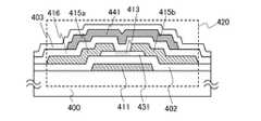
バックゲートを設けたトランジスタの断面図の一例を図9に示す。図9に示すトランジスタ420は、図8(D)に示すトランジスタ410にバックゲート441を追加した構造を有する。すなわち、図9に示すトランジスタ420は、絶縁表面を有する基板400上にゲート電極層411、ゲート絶縁層402、チャネル形成領域413を有する酸化物半導体層431、ソース電極層およびドレイン電極層415a、415b、酸化物絶縁層416、バックゲート441、保護絶縁層403を有する。FIG. 9 shows an example of a cross-sectional view of a transistor provided with a back gate. A
バックゲート441は、ゲート電極層411に用いることができる材料と同様の材料を用いて形成することができる。バックゲート441とチャネル形成領域の間に設けられている酸化物絶縁層416は、バックゲート441側のゲート絶縁層として機能する。よって、酸化物絶縁層416の厚さは、ゲート絶縁層と同程度とすることができる。その他の構成は、図8(D)に示すトランジスタ410と同様とすることができる。The
本実施の形態は、他の実施の形態、実施例と適宜組み合わせて実施することが可能である。This embodiment can be implemented in combination with any of the other embodiments and examples as appropriate.
本実施例では、開示する発明の一態様である半導体装置が有する酸化物半導体を用いたトランジスタの評価について、図10を参照して説明する。本実施例では、評価用素子(TEGともいう)を用いたオフ電流の測定値について以下に説明する。In this example, evaluation of a transistor including an oxide semiconductor included in a semiconductor device which is one embodiment of the disclosed invention will be described with reference to FIGS. In this example, a measurement value of off-state current using an evaluation element (also referred to as TEG) is described below.
評価用素子は、チャネル形成領域の長さと幅の関係がL/W=3μm/50μmのトランジスタを200個並列に接続することで作製した。この評価用素子は、L/W=3μm/10000μmのトランジスタに相当する。図10に評価用素子として作製されたトランジスタの初期特性を示す。トランジスタは高純度化された酸化物半導体層をチャネル形成領域に用いたものである。なお、ソース電極層又はドレイン電極層と酸化物半導体層とが重畳する領域のチャネル長方向における長さ(Lov)は1.5μmとした。The evaluation element was manufactured by connecting 200 transistors in which the relationship between the length and width of the channel formation region was L / W = 3 μm / 50 μm in parallel. This evaluation element corresponds to a transistor of L / W = 3 μm / 10000 μm. FIG. 10 shows initial characteristics of a transistor manufactured as an evaluation element. The transistor uses a highly purified oxide semiconductor layer for a channel formation region. Note that the length (Lov) in the channel length direction of the region where the source or drain electrode layer overlaps with the oxide semiconductor layer was 1.5 μm.
トランジスタの初期特性を測定するため、基板温度を室温とし、ソース−ドレイン間電圧(以下、ドレイン電圧またはVdという)を1Vまたは10Vとし、ソース−ゲート間電圧(以下、ゲート電圧またはVgという)を−20V〜+20Vまで変化させたときのソース−ドレイン電流(以下、ドレイン電流またはIdという)を測定し、Vg−Id特性を評価した。なお図10では、Vgが−20V〜+5Vまでの範囲でVg−Id特性を示している。In order to measure the initial characteristics of the transistor, the substrate temperature is set to room temperature, the source-drain voltage (hereinafter referred to as drain voltage or Vd) is set to 1 V or 10 V, and the source-gate voltage (hereinafter referred to as gate voltage or Vg) is set. Source-drain current (hereinafter referred to as drain current or Id) when changed from −20 V to +20 V was measured, and Vg-Id characteristics were evaluated. In FIG. 10, the Vg-Id characteristic is shown in the range of Vg from −20V to + 5V.
図10に示すようにチャネル幅Wが10000μmのトランジスタは、Vdが1Vおよび10Vにおいてオフ電流は1×10⁻¹³[A]以下となっており、測定機(半導体パラメータ・アナライザ、Agilent 4156C;Agilent社製)の検出限界以下となっている。すなわち、当該トランジスタのチャネル幅1μmあたりのオフ電流値は、10aA/μm以下であることがわかる。なお、チャネル長が3μm以上であれば、当該トランジスタのオフ電流値は10aA/μm以下であると見積もられることも付記する。As shown in FIG. 10, a transistor having a channel width W of 10000 μm has an off current of 1 × 10⁻¹³ [A] or less when Vd is 1 V and 10 V, and a measuring instrument (semiconductor parameter analyzer, Agilent 4156C; Agilent The detection limit of the product). That is, it can be seen that the off-current value per 1 μm channel width of the transistor is 10 aA / μm or less. Note that if the channel length is 3 μm or more, the off-state current value of the transistor is estimated to be 10 aA / μm or less.
また、チャネル幅Wが1000000μm(1m)のトランジスタについても同様に作製し測定した。その結果、オフ電流値は測定機の検出限界近傍である1×10⁻¹²[A]以下となることが確認された。すなわち、当該トランジスタのチャネル幅1μmあたりのオフ電流値は、1aA/μm以下であることがわかる。A transistor having a channel width W of 1,000,000 μm (1 m) was similarly manufactured and measured. As a result, it was confirmed that the off-current value was 1 × 10⁻¹² [A] or less, which is near the detection limit of the measuring machine. That is, it can be seen that the off-current value per 1 μm channel width of the transistor is 1 aA / μm or less.
図10に示すようにトランジスタのオフ電流が1×10⁻¹³[A]程度であるのは、上記作製工程において酸化物半導体層中における水素濃度を十分に低減できたためである。The reason why the off-state current of the transistor is approximately 1 × 10⁻¹³ [A] as illustrated in FIG. 10 is that the hydrogen concentration in the oxide semiconductor layer can be sufficiently reduced in the manufacturing process.
また、キャリア測定機で測定される酸化物半導体層のキャリア密度は、1×10¹²/cm3未満、あるいは1×1011/cm3未満である。即ち、酸化物半導体層のキャリア密度は、限りなくゼロに近くすることができる。The carrier density of the oxide semiconductor layer measured with a carrier measuring machine is less than 1 × 10¹² / cm3 , or less than 1 × 10¹¹ / cm3 . That is, the carrier density of the oxide semiconductor layer can be as close to zero as possible.
また、トランジスタのチャネル長Lを10nm以上1000nm以下とすることも可能である。これにより、回路の動作速度を高速化できる。また、オフ電流値が極めて小さいため、低消費電力化も図ることができる。Further, the channel length L of the transistor can be greater than or equal to 10 nm and less than or equal to 1000 nm. Thereby, the operation speed of the circuit can be increased. In addition, since the off-state current value is extremely small, power consumption can be reduced.
また、トランジスタのオフ状態において、酸化物半導体層を絶縁体とみなして回路設計を行うことができる。In addition, in the off state of the transistor, circuit design can be performed by regarding the oxide semiconductor layer as an insulator.
上記のように高純度化された酸化物半導体(purified OS)を用いたトランジスタは、オフ電流の温度依存性がほとんど現れない。これは、酸化物半導体が高純度化されることによって、導電型が限りなく真性に近づき、フェルミ準位が禁制帯の中央に位置するため、温度依存性を示さなくなると考えられる。また、これは、酸化物半導体のバンドギャップが大きく、熱励起キャリアが極めて少ないことにも起因する。As described above, a transistor using a purified oxide semiconductor (purified OS) hardly exhibits temperature dependency of off-state current. This is presumably because when the oxide semiconductor is highly purified, the conductivity type is as close to intrinsic as possible, and the Fermi level is located at the center of the forbidden band, so that temperature dependence is not exhibited. This is also because the oxide semiconductor has a large band gap and extremely few thermally excited carriers.
以上の結果は、キャリア密度を1×10¹²/cm3未満あるいは1×1011/cm3未満としたトランジスタが、室温におけるオフ電流値が1aA/μm以下であることを示すものである。また、当該トランジスタを半導体装置が有するトランジスタとして適用することで、新規な回路構成を有するフォトセンサを有する半導体装置を提供することができる。また、当該半導体装置の消費電力を低減することおよび表示の劣化(表示品質の低下)を抑制することが可能である。さらには、温度などの外部因子に起因する表示の劣化(変化)が低減された半導体装置を提供することが可能である。The above results indicate that a transistor having a carrier density of less than 1 × 10¹² / cm3 or less than 1 × 10¹¹ / cm3 has an off-current value of 1 aA / μm or less at room temperature. In addition, by applying the transistor as a transistor included in a semiconductor device, a semiconductor device including a photosensor having a novel circuit configuration can be provided. In addition, power consumption of the semiconductor device can be reduced and display deterioration (decrease in display quality) can be suppressed. Furthermore, it is possible to provide a semiconductor device in which display deterioration (change) due to external factors such as temperature is reduced.
100 表示装置
101 画素回路
102 表示素子制御回路
103 フォトセンサ制御回路
104 画素
105 表示素子
106 フォトセンサ
107 表示素子駆動回路
108 表示素子駆動回路
109 フォトセンサ読み出し回路
110 フォトセンサ駆動回路
200 プリチャージ回路
201 トランジスタ
202 保持容量
203 液晶素子
204 フォトダイオード
205 トランジスタ
206 トランジスタ
207 トランジスタ
208 ゲート信号線
209 ゲート信号線
210 フォトダイオードリセット信号線
211 ゲート信号線
212 ビデオデータ信号線
213 フォトセンサ基準信号線
214 フォトセンサ出力信号線
215 ゲート信号線
216 トランジスタ
217 プリチャージ信号線
218 バックゲート信号線
301 信号
302 信号
303 信号
304 信号
305 信号
306 信号
307 信号
400 基板
402 ゲート絶縁層
403 保護絶縁層
410 トランジスタ
411 ゲート電極層
413 チャネル形成領域
416 酸化物絶縁層
420 トランジスタ
430 酸化物半導体膜
431 酸化物半導体層
441 バックゲート
415a ソース電極層又はドレイン電極層
415b ソース電極層又はドレイン電極層
501 信号
502 信号
503 信号
504 信号
505 信号
506 信号
507 信号
508 信号
509 信号
510 期間
511 期間
512 期間
513 期間
601 トランジスタ
801 信号
802 信号
803 信号
804 信号
805 信号
806 信号
807 信号
808 信号
809 信号
810 期間
811 期間
812 期間
813 期間DESCRIPTION OF SYMBOLS 100
Claims (7)
Translated fromJapanese前記フォトダイオードは、光の強度に応じた電気信号を生成する機能を有し、
前記第1のトランジスタは、ゲートに電荷を蓄積する機能と、蓄積された電荷を出力信号に変換する機能と、を有し、
前記第2のトランジスタは、前記フォトダイオードから生成された電気信号を前記第1のトランジスタのゲートに転送する機能と、前記第1のトランジスタのゲートに蓄積された電荷を保持する機能と、を有し、
前記第1のトランジスタは、バックゲートを有し、
前記第2のトランジスタは、酸化物半導体層により形成されたチャネル形成領域を有することを特徴とする半導体装置。A photodiode, a first transistor, and a second transistor;
The photodiode has a function of generating an electrical signal corresponding to the intensity of light,
The first transistor has a function of accumulating charges in a gate and a function of converting the accumulated charges into an output signal.
The second transistor has a function of transferring an electric signal generated from the photodiode to the gate of the first transistor and a function of holding electric charge accumulated in the gate of the first transistor. And
The first transistor has a back gate;
The semiconductor device, wherein the second transistor includes a channel formation region formed using an oxide semiconductor layer.
前記フォトダイオードは、光の強度に応じた電気信号を生成する機能を有し、
前記第1のトランジスタは、ゲートに電荷を蓄積する機能と、蓄積された電荷を出力信号に変換する機能と、を有し、
前記第2のトランジスタは、前記フォトダイオードから生成された電気信号を前記第1のトランジスタのゲートに転送する機能と、前記第1のトランジスタのゲートに蓄積された電荷を保持する機能と、を有し、
前記第3のトランジスタは、前記出力信号の読み出しを制御する機能を有し、
前記第1のトランジスタは、バックゲートを有し、
前記第2のトランジスタは、酸化物半導体層により形成されたチャネル形成領域を有することを特徴とする半導体装置。A photodiode, a first transistor, a second transistor, and a third transistor;
The photodiode has a function of generating an electrical signal corresponding to the intensity of light,
The first transistor has a function of accumulating charges in a gate and a function of converting the accumulated charges into an output signal.
The second transistor has a function of transferring an electric signal generated from the photodiode to the gate of the first transistor and a function of holding electric charge accumulated in the gate of the first transistor. And
The third transistor has a function of controlling reading of the output signal,
The first transistor has a back gate;
The semiconductor device, wherein the second transistor includes a channel formation region formed using an oxide semiconductor layer.
前記フォトセンサはリセット動作、前記第1のトランジスタのゲートに電荷を蓄積する累積動作、および読み出し動作を行う機能を有し、
前記累積動作は、前記第2のトランジスタにより制御され、
前記第1のトランジスタは、バックゲートを有し、
1回の撮像を行う期間において、前記バックゲートの電位を変更しながら前記読み出し動作が複数回行われ、
前記第2のトランジスタは、酸化物半導体層により形成されたチャネル形成領域を有することを特徴とする半導体装置。A photosensor having a first transistor and a second transistor;
The photosensor has a function of performing a reset operation, a cumulative operation for accumulating charges in the gate of the first transistor, and a read operation,
The cumulative operation is controlled by the second transistor,
The first transistor has a back gate;
The readout operation is performed a plurality of times while changing the potential of the back gate in the period of performing one imaging.
The semiconductor device, wherein the second transistor includes a channel formation region formed using an oxide semiconductor layer.
前記複数のフォトセンサは、前記リセット動作を共通して行い、前記累積動作を共通して行い、前記読み出し動作を順次行う機能を有することを特徴とする半導体装置。In Claim 4, It has multiple said photosensors,
The plurality of photosensors have a function of performing the reset operation in common, performing the accumulation operation in common, and sequentially performing the read operation.
第2のトランジスタを非導通状態として前記第1のトランジスタのゲートに蓄積された電荷を保持し、
前記第1のトランジスタのバックゲートの電位を第1の電位に設定し、前記第1のトランジスタのゲートに蓄積され保持された前記電荷を第1の出力信号に変換し、前記第1の出力信号を読み出し、
前記第1のトランジスタのバックゲートの電位を第2の電位に設定し、前記第1のトランジスタのゲートに蓄積され保持された前記電荷を第2の出力信号に変換し、前記第2の出力信号を読み出すことを特徴とする半導体装置の駆動方法。Transferring the electrical signal generated from the photodiode to the gate of the first transistor;
Holding the charge accumulated in the gate of the first transistor with the second transistor non-conductive;
The potential of the back gate of the first transistor is set to a first potential, the charge accumulated and held in the gate of the first transistor is converted into a first output signal, and the first output signal Read
The potential of the back gate of the first transistor is set to a second potential, the charge accumulated and held in the gate of the first transistor is converted into a second output signal, and the second output signal A method for driving a semiconductor device, comprising:
Priority Applications (1)
| Application Number | Priority Date | Filing Date | Title |
|---|---|---|---|
| JP2011025070AJP5667464B2 (en) | 2010-02-12 | 2011-02-08 | Semiconductor device and driving method thereof |
Applications Claiming Priority (3)
| Application Number | Priority Date | Filing Date | Title |
|---|---|---|---|
| JP2010028762 | 2010-02-12 | ||
| JP2010028762 | 2010-02-12 | ||
| JP2011025070AJP5667464B2 (en) | 2010-02-12 | 2011-02-08 | Semiconductor device and driving method thereof |
Related Child Applications (1)
| Application Number | Title | Priority Date | Filing Date |
|---|---|---|---|
| JP2014251750ADivisionJP5825748B2 (en) | 2010-02-12 | 2014-12-12 | Semiconductor device |
Publications (2)
| Publication Number | Publication Date |
|---|---|
| JP2011187944Atrue JP2011187944A (en) | 2011-09-22 |
| JP5667464B2 JP5667464B2 (en) | 2015-02-12 |
Family
ID=44367622
Family Applications (4)
| Application Number | Title | Priority Date | Filing Date |
|---|---|---|---|
| JP2011025070AExpired - Fee RelatedJP5667464B2 (en) | 2010-02-12 | 2011-02-08 | Semiconductor device and driving method thereof |
| JP2014251750AActiveJP5825748B2 (en) | 2010-02-12 | 2014-12-12 | Semiconductor device |
| JP2015201638AActiveJP6002828B2 (en) | 2010-02-12 | 2015-10-12 | Semiconductor device |
| JP2016172433AExpired - Fee RelatedJP6215420B2 (en) | 2010-02-12 | 2016-09-05 | Semiconductor device |
Family Applications After (3)
| Application Number | Title | Priority Date | Filing Date |
|---|---|---|---|
| JP2014251750AActiveJP5825748B2 (en) | 2010-02-12 | 2014-12-12 | Semiconductor device |
| JP2015201638AActiveJP6002828B2 (en) | 2010-02-12 | 2015-10-12 | Semiconductor device |
| JP2016172433AExpired - Fee RelatedJP6215420B2 (en) | 2010-02-12 | 2016-09-05 | Semiconductor device |
Country Status (6)
| Country | Link |
|---|---|
| US (4) | US8586905B2 (en) |
| JP (4) | JP5667464B2 (en) |
| KR (1) | KR101924318B1 (en) |
| CN (2) | CN105336744B (en) |
| TW (2) | TWI556416B (en) |
| WO (1) | WO2011099336A1 (en) |
Cited By (5)
| Publication number | Priority date | Publication date | Assignee | Title |
|---|---|---|---|---|
| JP2013175160A (en)* | 2011-12-26 | 2013-09-05 | Semiconductor Energy Lab Co Ltd | Motion recognition device |
| JP2016197722A (en)* | 2015-04-03 | 2016-11-24 | 株式会社半導体エネルギー研究所 | Imaging device and electronic equipment |
| JPWO2020241165A1 (en)* | 2019-05-24 | 2020-12-03 | ||
| JP2022010017A (en)* | 2013-06-05 | 2022-01-14 | 株式会社半導体エネルギー研究所 | Semiconductor device |
| WO2023054230A1 (en)* | 2021-09-29 | 2023-04-06 | 株式会社 Rosnes | Imaging device |
Families Citing this family (41)
| Publication number | Priority date | Publication date | Assignee | Title |
|---|---|---|---|---|
| WO2011099343A1 (en)* | 2010-02-12 | 2011-08-18 | Semiconductor Energy Laboratory Co., Ltd. | Semiconductor device and driving method thereof |
| US8803063B2 (en)* | 2010-02-19 | 2014-08-12 | Semiconductor Energy Laboratory Co., Ltd. | Photodetector circuit |
| KR101773992B1 (en) | 2010-03-12 | 2017-09-01 | 가부시키가이샤 한도오따이 에네루기 켄큐쇼 | Semiconductor device |
| DE112011102837B4 (en) | 2010-08-27 | 2021-03-11 | Semiconductor Energy Laboratory Co., Ltd. | Memory device and semiconductor device with double gate and oxide semiconductor |
| JP2012256020A (en)* | 2010-12-15 | 2012-12-27 | Semiconductor Energy Lab Co Ltd | Semiconductor device and driving method for the same |
| JP5560227B2 (en)* | 2011-04-11 | 2014-07-23 | 株式会社ジャパンディスプレイ | Method for manufacturing liquid crystal display device and liquid crystal display device |
| US8836626B2 (en) | 2011-07-15 | 2014-09-16 | Semiconductor Energy Laboratory Co., Ltd. | Semiconductor device and method for driving the same |
| JP6151530B2 (en) | 2012-02-29 | 2017-06-21 | 株式会社半導体エネルギー研究所 | Image sensor, camera, and surveillance system |
| CN107340509B (en)* | 2012-03-09 | 2020-04-14 | 株式会社半导体能源研究所 | Driving method of semiconductor device |
| US9236408B2 (en) | 2012-04-25 | 2016-01-12 | Semiconductor Energy Laboratory Co., Ltd. | Oxide semiconductor device including photodiode |
| DE102013110695A1 (en) | 2012-10-02 | 2014-04-03 | Samsung Electronics Co., Ltd. | Image sensor, method for operating the same and image processing system with the same |
| TWI597849B (en)* | 2012-12-28 | 2017-09-01 | 神戶製鋼所股份有限公司 | Thin film transistor and method of manufacturing the same |
| US20140263952A1 (en)* | 2013-03-14 | 2014-09-18 | Perkinelmer Holdings, Inc. | High performance digital imaging system |
| JPWO2015025499A1 (en)* | 2013-08-19 | 2017-03-02 | 出光興産株式会社 | Oxide semiconductor substrate and Schottky barrier diode |
| US20160013243A1 (en)* | 2014-03-10 | 2016-01-14 | Dpix, Llc | Photosensor arrays for detection of radiation and process for the preparation thereof |
| JP6612056B2 (en) | 2014-05-16 | 2019-11-27 | 株式会社半導体エネルギー研究所 | Imaging device and monitoring device |
| US9881954B2 (en) | 2014-06-11 | 2018-01-30 | Semiconductor Energy Laboratory Co., Ltd. | Imaging device |
| TWI757788B (en)* | 2014-06-27 | 2022-03-11 | 日商半導體能源研究所股份有限公司 | Imaging device and electronic device |
| JP2016029795A (en) | 2014-07-18 | 2016-03-03 | 株式会社半導体エネルギー研究所 | Semiconductor device, imaging device, and electronic apparatus |
| JP6552336B2 (en) | 2014-08-29 | 2019-07-31 | 株式会社半導体エネルギー研究所 | Semiconductor device |
| US9761730B2 (en) | 2014-10-29 | 2017-09-12 | Semiconductor Energy Laboratory Co., Ltd. | Imaging device and electronic device |
| US9529079B1 (en)* | 2015-03-26 | 2016-12-27 | Google Inc. | Multiplexed multichannel photodetector |
| US10306168B2 (en) | 2015-05-04 | 2019-05-28 | Semiconductor Energy Laboratory Co., Ltd. | Semiconductor device, imaging system, and electronic device |
| TWI713367B (en) | 2015-07-07 | 2020-12-11 | 日商半導體能源研究所股份有限公司 | Imaging device and operating method thereof |
| US10163948B2 (en)* | 2015-07-23 | 2018-12-25 | Semiconductor Energy Laboratory Co., Ltd. | Imaging device and electronic device |
| US9786856B2 (en) | 2015-08-20 | 2017-10-10 | Dpix, Llc | Method of manufacturing an image sensor device |
| US10090344B2 (en) | 2015-09-07 | 2018-10-02 | Semiconductor Energy Laboratory Co., Ltd. | Imaging device, method for operating the same, module, and electronic device |
| US10896923B2 (en) | 2015-09-18 | 2021-01-19 | Semiconductor Energy Laboratory Co., Ltd. | Method of operating an imaging device with global shutter system |
| US10109667B2 (en) | 2015-10-09 | 2018-10-23 | Semiconductor Energy Laboratory Co., Ltd. | Imaging device, module, and electronic device |
| JP6796461B2 (en) | 2015-11-18 | 2020-12-09 | 株式会社半導体エネルギー研究所 | Semiconductor devices, computers and electronic devices |
| US10014325B2 (en)* | 2016-03-10 | 2018-07-03 | Semiconductor Energy Laboratory Co., Ltd. | Semiconductor device and electronic device |
| WO2017159625A1 (en)* | 2016-03-15 | 2017-09-21 | シャープ株式会社 | Active matrix substrate |
| SG10201701689UA (en) | 2016-03-18 | 2017-10-30 | Semiconductor Energy Lab | Semiconductor device, semiconductor wafer, and electronic device |
| US10242617B2 (en)* | 2016-06-03 | 2019-03-26 | Semiconductor Energy Laboratory Co., Ltd. | Display device, display module, electronic device, and driving method |
| US9929215B2 (en) | 2016-07-12 | 2018-03-27 | Dpix, Llc | Method of optimizing an interface for processing of an organic semiconductor |
| US10403204B2 (en)* | 2016-07-12 | 2019-09-03 | Semiconductor Energy Laboratory Co., Ltd. | Display device, display module, electronic device, and method for driving display device |
| KR20180055701A (en) | 2016-11-17 | 2018-05-25 | 가부시키가이샤 한도오따이 에네루기 켄큐쇼 | Semiconductor device and method of manufacturing the same |
| CN107687893B (en)* | 2017-09-25 | 2020-11-06 | 南京科兴新材料科技有限公司 | Array sensor |
| CN110926508B (en)* | 2019-11-28 | 2021-11-19 | 北京大学深圳研究生院 | Active driving type photoelectric sensor, front end circuit and driving method |
| KR20220117921A (en)* | 2019-12-24 | 2022-08-24 | 가부시키가이샤 한도오따이 에네루기 켄큐쇼 | display device |
| CN112532899B (en)* | 2020-11-27 | 2023-06-30 | 京东方科技集团股份有限公司 | Photoelectric conversion circuit, driving method, photoelectric detection substrate, photoelectric detection device |
Citations (6)
| Publication number | Priority date | Publication date | Assignee | Title |
|---|---|---|---|---|
| JPH11195778A (en)* | 1997-10-30 | 1999-07-21 | Ino Vision Kk | Solid-state image-pickup device and detection of light signal therefrom |
| JP2006050544A (en)* | 2004-07-05 | 2006-02-16 | Konica Minolta Holdings Inc | Solid-state imaging device and camera equipped with the same |
| JP2008283593A (en)* | 2007-05-14 | 2008-11-20 | Konica Minolta Holdings Inc | Solid-state imaging device |
| JP2009206508A (en)* | 2008-01-31 | 2009-09-10 | Canon Inc | Thin film transistor and display |
| JP2009535819A (en)* | 2006-08-31 | 2009-10-01 | マイクロン テクノロジー, インク. | Transparent channel thin film transistor based pixels for high performance image sensors |
| JP2010074138A (en)* | 2008-08-19 | 2010-04-02 | Fujifilm Corp | Thin-film transistor, active matrix substrate, and imaging apparatus |
Family Cites Families (149)
| Publication number | Priority date | Publication date | Assignee | Title |
|---|---|---|---|---|
| JPS60198861A (en) | 1984-03-23 | 1985-10-08 | Fujitsu Ltd | Thin film transistor |
| JPH0244256B2 (en) | 1987-01-28 | 1990-10-03 | Kagaku Gijutsucho Mukizaishitsu Kenkyushocho | INGAZN2O5DESHIMESARERUROTSUHOSHOKEINOSOJOKOZOOJUSURUKAGOBUTSUOYOBISONOSEIZOHO |
| JPS63210023A (en) | 1987-02-24 | 1988-08-31 | Natl Inst For Res In Inorg Mater | Compound having a hexagonal layered structure represented by InGaZn↓4O↓7 and its manufacturing method |
| JPH0244260B2 (en) | 1987-02-24 | 1990-10-03 | Kagaku Gijutsucho Mukizaishitsu Kenkyushocho | INGAZN5O8DESHIMESARERUROTSUHOSHOKEINOSOJOKOZOOJUSURUKAGOBUTSUOYOBISONOSEIZOHO |
| JPH0244258B2 (en) | 1987-02-24 | 1990-10-03 | Kagaku Gijutsucho Mukizaishitsu Kenkyushocho | INGAZN3O6DESHIMESARERUROTSUHOSHOKEINOSOJOKOZOOJUSURUKAGOBUTSUOYOBISONOSEIZOHO |
| JPH0244262B2 (en) | 1987-02-27 | 1990-10-03 | Kagaku Gijutsucho Mukizaishitsu Kenkyushocho | INGAZN6O9DESHIMESARERUROTSUHOSHOKEINOSOJOKOZOOJUSURUKAGOBUTSUOYOBISONOSEIZOHO |
| JPH0244263B2 (en) | 1987-04-22 | 1990-10-03 | Kagaku Gijutsucho Mukizaishitsu Kenkyushocho | INGAZN7O10DESHIMESARERUROTSUHOSHOKEINOSOJOKOZOOJUSURUKAGOBUTSUOYOBISONOSEIZOHO |
| JPH05251705A (en) | 1992-03-04 | 1993-09-28 | Fuji Xerox Co Ltd | Thin-film transistor |
| WO1995022176A1 (en) | 1994-02-11 | 1995-08-17 | Litton Systems Canada Limited | Electromagnetic radiation imaging device using dual gate thin film transistors |
| JP3525500B2 (en)* | 1994-07-26 | 2004-05-10 | ミノルタ株式会社 | Solid-state imaging device |
| JP3479375B2 (en) | 1995-03-27 | 2003-12-15 | 科学技術振興事業団 | Metal oxide semiconductor device in which a pn junction is formed with a thin film transistor made of a metal oxide semiconductor such as cuprous oxide, and methods for manufacturing the same |
| KR100394896B1 (en) | 1995-08-03 | 2003-11-28 | 코닌클리케 필립스 일렉트로닉스 엔.브이. | A semiconductor device including a transparent switching element |
| JP3625598B2 (en) | 1995-12-30 | 2005-03-02 | 三星電子株式会社 | Manufacturing method of liquid crystal display device |
| US6051857A (en) | 1998-01-07 | 2000-04-18 | Innovision, Inc. | Solid-state imaging device and method of detecting optical signals using the same |
| JP2001051292A (en) | 1998-06-12 | 2001-02-23 | Semiconductor Energy Lab Co Ltd | Semiconductor device and semiconductor display device |
| JP4170454B2 (en) | 1998-07-24 | 2008-10-22 | Hoya株式会社 | Article having transparent conductive oxide thin film and method for producing the same |
| JP2000150861A (en) | 1998-11-16 | 2000-05-30 | Tdk Corp | Oxide thin film |
| JP3276930B2 (en) | 1998-11-17 | 2002-04-22 | 科学技術振興事業団 | Transistor and semiconductor device |
| TW460731B (en) | 1999-09-03 | 2001-10-21 | Ind Tech Res Inst | Electrode structure and production method of wide viewing angle LCD |
| JP4112184B2 (en) | 2000-01-31 | 2008-07-02 | 株式会社半導体エネルギー研究所 | Area sensor and display device |
| US6747638B2 (en) | 2000-01-31 | 2004-06-08 | Semiconductor Energy Laboratory Co., Ltd. | Adhesion type area sensor and display device having adhesion type area sensor |
| JP2001326343A (en) | 2000-05-16 | 2001-11-22 | Minolta Co Ltd | Solid-state imaging device |
| JP4089858B2 (en) | 2000-09-01 | 2008-05-28 | 国立大学法人東北大学 | Semiconductor device |
| KR20020038482A (en) | 2000-11-15 | 2002-05-23 | 모리시타 요이찌 | Thin film transistor array, method for producing the same, and display panel using the same |
| JP4302346B2 (en)* | 2000-12-14 | 2009-07-22 | 株式会社半導体エネルギー研究所 | Semiconductor devices, electronic equipment |
| US6724012B2 (en) | 2000-12-14 | 2004-04-20 | Semiconductor Energy Laboratory Co., Ltd. | Display matrix with pixels having sensor and light emitting portions |
| JP3899236B2 (en) | 2001-02-16 | 2007-03-28 | シャープ株式会社 | Manufacturing method of image sensor |
| JP3997731B2 (en) | 2001-03-19 | 2007-10-24 | 富士ゼロックス株式会社 | Method for forming a crystalline semiconductor thin film on a substrate |
| JP2002289859A (en) | 2001-03-23 | 2002-10-04 | Minolta Co Ltd | Thin film transistor |
| US6794682B2 (en) | 2001-04-04 | 2004-09-21 | Canon Kabushiki Kaisha | Semiconductor device, method for manufacturing the same, and radiation detector |
| JP2002368229A (en)* | 2001-04-04 | 2002-12-20 | Canon Inc | Semiconductor device, manufacturing method thereof, and radiation detection device |
| JP3925839B2 (en) | 2001-09-10 | 2007-06-06 | シャープ株式会社 | Semiconductor memory device and test method thereof |
| JP4090716B2 (en) | 2001-09-10 | 2008-05-28 | 雅司 川崎 | Thin film transistor and matrix display device |
| JP4164562B2 (en) | 2002-09-11 | 2008-10-15 | 独立行政法人科学技術振興機構 | Transparent thin film field effect transistor using homologous thin film as active layer |
| WO2003040441A1 (en) | 2001-11-05 | 2003-05-15 | Japan Science And Technology Agency | Natural superlattice homologous single crystal thin film, method for preparation thereof, and device using said single crystal thin film |
| JP4083486B2 (en) | 2002-02-21 | 2008-04-30 | 独立行政法人科学技術振興機構 | Method for producing LnCuO (S, Se, Te) single crystal thin film |
| CN1445821A (en) | 2002-03-15 | 2003-10-01 | 三洋电机株式会社 | Forming method of ZnO film and ZnO semiconductor layer, semiconductor element and manufacturing method thereof |
| JP3933591B2 (en) | 2002-03-26 | 2007-06-20 | 淳二 城戸 | Organic electroluminescent device |
| US7339187B2 (en) | 2002-05-21 | 2008-03-04 | State Of Oregon Acting By And Through The Oregon State Board Of Higher Education On Behalf Of Oregon State University | Transistor structures |
| JP2004022625A (en) | 2002-06-13 | 2004-01-22 | Murata Mfg Co Ltd | Semiconductor device and method of manufacturing the semiconductor device |
| US7105868B2 (en) | 2002-06-24 | 2006-09-12 | Cermet, Inc. | High-electron mobility transistor with zinc oxide |
| US7067843B2 (en) | 2002-10-11 | 2006-06-27 | E. I. Du Pont De Nemours And Company | Transparent oxide semiconductor thin film transistors |
| JP2004165911A (en)* | 2002-11-12 | 2004-06-10 | Canon Inc | Driving method of transistor |
| US6995053B2 (en)* | 2004-04-23 | 2006-02-07 | Sharp Laboratories Of America, Inc. | Vertical thin film transistor |
| JP4266656B2 (en) | 2003-02-14 | 2009-05-20 | キヤノン株式会社 | Solid-state imaging device and radiation imaging device |
| JP4166105B2 (en) | 2003-03-06 | 2008-10-15 | シャープ株式会社 | Semiconductor device and manufacturing method thereof |
| JP2004273732A (en) | 2003-03-07 | 2004-09-30 | Sharp Corp | Active matrix substrate and manufacturing method thereof |
| JP4108633B2 (en) | 2003-06-20 | 2008-06-25 | シャープ株式会社 | THIN FILM TRANSISTOR, MANUFACTURING METHOD THEREOF, AND ELECTRONIC DEVICE |
| US7262463B2 (en) | 2003-07-25 | 2007-08-28 | Hewlett-Packard Development Company, L.P. | Transistor including a deposited channel region having a doped portion |
| US7115923B2 (en)* | 2003-08-22 | 2006-10-03 | Micron Technology, Inc. | Imaging with gate controlled charge storage |
| US7297977B2 (en) | 2004-03-12 | 2007-11-20 | Hewlett-Packard Development Company, L.P. | Semiconductor device |
| US7145174B2 (en) | 2004-03-12 | 2006-12-05 | Hewlett-Packard Development Company, Lp. | Semiconductor device |
| CN1998087B (en) | 2004-03-12 | 2014-12-31 | 独立行政法人科学技术振兴机构 | Amorphous oxide and thin film transistor |
| US7282782B2 (en) | 2004-03-12 | 2007-10-16 | Hewlett-Packard Development Company, L.P. | Combined binary oxide semiconductor device |
| CN1678037A (en)* | 2004-04-02 | 2005-10-05 | 安捷伦科技有限公司 | Active Pixel Sensor Circuit |
| US7211825B2 (en) | 2004-06-14 | 2007-05-01 | Yi-Chi Shih | Indium oxide-based thin film transistors and circuits |
| JP2006100760A (en) | 2004-09-02 | 2006-04-13 | Casio Comput Co Ltd | Thin film transistor and manufacturing method thereof |
| US7285501B2 (en) | 2004-09-17 | 2007-10-23 | Hewlett-Packard Development Company, L.P. | Method of forming a solution processed device |
| US7298084B2 (en) | 2004-11-02 | 2007-11-20 | 3M Innovative Properties Company | Methods and displays utilizing integrated zinc oxide row and column drivers in conjunction with organic light emitting diodes |
| EP2453481B1 (en) | 2004-11-10 | 2017-01-11 | Canon Kabushiki Kaisha | Field effect transistor with amorphous oxide |
| US7829444B2 (en) | 2004-11-10 | 2010-11-09 | Canon Kabushiki Kaisha | Field effect transistor manufacturing method |
| US7791072B2 (en) | 2004-11-10 | 2010-09-07 | Canon Kabushiki Kaisha | Display |
| KR100953596B1 (en) | 2004-11-10 | 2010-04-21 | 캐논 가부시끼가이샤 | Light emitting device |
| US7863611B2 (en) | 2004-11-10 | 2011-01-04 | Canon Kabushiki Kaisha | Integrated circuits utilizing amorphous oxides |
| US7453065B2 (en) | 2004-11-10 | 2008-11-18 | Canon Kabushiki Kaisha | Sensor and image pickup device |
| AU2005302964B2 (en) | 2004-11-10 | 2010-11-04 | Canon Kabushiki Kaisha | Field effect transistor employing an amorphous oxide |
| US7579224B2 (en) | 2005-01-21 | 2009-08-25 | Semiconductor Energy Laboratory Co., Ltd. | Method for manufacturing a thin film semiconductor device |
| TWI505473B (en) | 2005-01-28 | 2015-10-21 | Semiconductor Energy Lab | Semiconductor device, electronic device, and method of manufacturing semiconductor device |
| TWI445178B (en) | 2005-01-28 | 2014-07-11 | Semiconductor Energy Lab | Semiconductor device, electronic device, and method of manufacturing semiconductor device |
| US7858451B2 (en) | 2005-02-03 | 2010-12-28 | Semiconductor Energy Laboratory Co., Ltd. | Electronic device, semiconductor device and manufacturing method thereof |
| US7948171B2 (en) | 2005-02-18 | 2011-05-24 | Semiconductor Energy Laboratory Co., Ltd. | Light emitting device |
| US20060197092A1 (en) | 2005-03-03 | 2006-09-07 | Randy Hoffman | System and method for forming conductive material on a substrate |
| US8681077B2 (en) | 2005-03-18 | 2014-03-25 | Semiconductor Energy Laboratory Co., Ltd. | Semiconductor device, and display device, driving method and electronic apparatus thereof |
| US7544967B2 (en) | 2005-03-28 | 2009-06-09 | Massachusetts Institute Of Technology | Low voltage flexible organic/transparent transistor for selective gas sensing, photodetecting and CMOS device applications |
| US7645478B2 (en) | 2005-03-31 | 2010-01-12 | 3M Innovative Properties Company | Methods of making displays |
| US8300031B2 (en) | 2005-04-20 | 2012-10-30 | Semiconductor Energy Laboratory Co., Ltd. | Semiconductor device comprising transistor having gate and drain connected through a current-voltage conversion element |
| JP2006344849A (en) | 2005-06-10 | 2006-12-21 | Casio Comput Co Ltd | Thin film transistor |
| US7402506B2 (en) | 2005-06-16 | 2008-07-22 | Eastman Kodak Company | Methods of making thin film transistors comprising zinc-oxide-based semiconductor materials and transistors made thereby |
| US7691666B2 (en) | 2005-06-16 | 2010-04-06 | Eastman Kodak Company | Methods of making thin film transistors comprising zinc-oxide-based semiconductor materials and transistors made thereby |
| US7507618B2 (en) | 2005-06-27 | 2009-03-24 | 3M Innovative Properties Company | Method for making electronic devices using metal oxide nanoparticles |
| FR2888989B1 (en) | 2005-07-21 | 2008-06-06 | St Microelectronics Sa | IMAGE SENSOR |
| KR100711890B1 (en) | 2005-07-28 | 2007-04-25 | 삼성에스디아이 주식회사 | OLED display and manufacturing method thereof |
| JP2007059128A (en) | 2005-08-23 | 2007-03-08 | Canon Inc | Organic EL display device and manufacturing method thereof |
| JP5116225B2 (en) | 2005-09-06 | 2013-01-09 | キヤノン株式会社 | Manufacturing method of oxide semiconductor device |
| JP4850457B2 (en) | 2005-09-06 | 2012-01-11 | キヤノン株式会社 | Thin film transistor and thin film diode |
| JP2007073705A (en) | 2005-09-06 | 2007-03-22 | Canon Inc | Oxide semiconductor channel thin film transistor and method for manufacturing the same |
| JP4280736B2 (en) | 2005-09-06 | 2009-06-17 | キヤノン株式会社 | Semiconductor element |
| EP1770788A3 (en) | 2005-09-29 | 2011-09-21 | Semiconductor Energy Laboratory Co., Ltd. | Semiconductor device having oxide semiconductor layer and manufacturing method thereof |
| JP5037808B2 (en) | 2005-10-20 | 2012-10-03 | キヤノン株式会社 | Field effect transistor using amorphous oxide, and display device using the transistor |
| CN101577231B (en) | 2005-11-15 | 2013-01-02 | 株式会社半导体能源研究所 | Semiconductor device and method of manufacturing the same |
| TWI292281B (en) | 2005-12-29 | 2008-01-01 | Ind Tech Res Inst | Pixel structure of active organic light emitting diode and method of fabricating the same |
| US20070152133A1 (en)* | 2005-12-30 | 2007-07-05 | Motorola, Inc. | Image sensor array with ferroelectric elements and method therefor |
| US7867636B2 (en) | 2006-01-11 | 2011-01-11 | Murata Manufacturing Co., Ltd. | Transparent conductive film and method for manufacturing the same |
| JP4977478B2 (en) | 2006-01-21 | 2012-07-18 | 三星電子株式会社 | ZnO film and method of manufacturing TFT using the same |
| US7576394B2 (en) | 2006-02-02 | 2009-08-18 | Kochi Industrial Promotion Center | Thin film transistor including low resistance conductive thin films and manufacturing method thereof |
| US7977169B2 (en) | 2006-02-15 | 2011-07-12 | Kochi Industrial Promotion Center | Semiconductor device including active layer made of zinc oxide with controlled orientations and manufacturing method thereof |
| KR20070101595A (en) | 2006-04-11 | 2007-10-17 | 삼성전자주식회사 | ZnO TFT |
| US20070252928A1 (en) | 2006-04-28 | 2007-11-01 | Toppan Printing Co., Ltd. | Structure, transmission type liquid crystal display, reflection type display and manufacturing method thereof |
| JP5028033B2 (en) | 2006-06-13 | 2012-09-19 | キヤノン株式会社 | Oxide semiconductor film dry etching method |
| JP4609797B2 (en) | 2006-08-09 | 2011-01-12 | Nec液晶テクノロジー株式会社 | Thin film device and manufacturing method thereof |
| JP4999400B2 (en) | 2006-08-09 | 2012-08-15 | キヤノン株式会社 | Oxide semiconductor film dry etching method |
| JP4332545B2 (en) | 2006-09-15 | 2009-09-16 | キヤノン株式会社 | Field effect transistor and manufacturing method thereof |
| JP5164357B2 (en) | 2006-09-27 | 2013-03-21 | キヤノン株式会社 | Semiconductor device and manufacturing method of semiconductor device |
| JP4274219B2 (en) | 2006-09-27 | 2009-06-03 | セイコーエプソン株式会社 | Electronic devices, organic electroluminescence devices, organic thin film semiconductor devices |
| US7622371B2 (en) | 2006-10-10 | 2009-11-24 | Hewlett-Packard Development Company, L.P. | Fused nanocrystal thin film semiconductor and method |
| US7772021B2 (en) | 2006-11-29 | 2010-08-10 | Samsung Electronics Co., Ltd. | Flat panel displays comprising a thin-film transistor having a semiconductive oxide in its channel and methods of fabricating the same for use in flat panel displays |
| JP2008140684A (en) | 2006-12-04 | 2008-06-19 | Toppan Printing Co Ltd | Color EL display and manufacturing method thereof |
| US20080158217A1 (en) | 2006-12-28 | 2008-07-03 | Semiconductor Energy Laboratory Co., Ltd. | Display device |
| KR101303578B1 (en) | 2007-01-05 | 2013-09-09 | 삼성전자주식회사 | Etching method of thin film |
| US8207063B2 (en) | 2007-01-26 | 2012-06-26 | Eastman Kodak Company | Process for atomic layer deposition |
| KR100851215B1 (en) | 2007-03-14 | 2008-08-07 | 삼성에스디아이 주식회사 | Thin film transistor and organic light emitting display device using same |
| US7795613B2 (en) | 2007-04-17 | 2010-09-14 | Toppan Printing Co., Ltd. | Structure with transistor |
| KR101325053B1 (en) | 2007-04-18 | 2013-11-05 | 삼성디스플레이 주식회사 | Thin film transistor substrate and manufacturing method thereof |
| KR20080094300A (en) | 2007-04-19 | 2008-10-23 | 삼성전자주식회사 | Thin film transistors and methods of manufacturing the same and flat panel displays comprising thin film transistors |
| KR101334181B1 (en) | 2007-04-20 | 2013-11-28 | 삼성전자주식회사 | Thin Film Transistor having selectively crystallized channel layer and method of manufacturing the same |
| CN101663762B (en) | 2007-04-25 | 2011-09-21 | 佳能株式会社 | Oxynitride semiconductor |
| KR101345376B1 (en) | 2007-05-29 | 2013-12-24 | 삼성전자주식회사 | Fabrication method of ZnO family Thin film transistor |
| TWI341406B (en)* | 2007-07-23 | 2011-05-01 | Au Optronics Corp | Diaply panel and its application |
| US20100027355A1 (en) | 2007-07-31 | 2010-02-04 | Dao Thuy B | Planar double gate transistor storage cell |
| JP2009055190A (en)* | 2007-08-24 | 2009-03-12 | Nec Electronics Corp | Variable gain circuit |
| KR20090040158A (en) | 2007-10-19 | 2009-04-23 | 삼성전자주식회사 | CMOS image sensor with transparent transistor |
| EP2071441A1 (en) | 2007-12-03 | 2009-06-17 | Semiconductor Energy Laboratory Co., Ltd. | Mobile phone |
| JP5213422B2 (en) | 2007-12-04 | 2013-06-19 | キヤノン株式会社 | Oxide semiconductor element having insulating layer and display device using the same |
| US8202365B2 (en) | 2007-12-17 | 2012-06-19 | Fujifilm Corporation | Process for producing oriented inorganic crystalline film, and semiconductor device using the oriented inorganic crystalline film |
| JP2009169400A (en) | 2007-12-18 | 2009-07-30 | Sony Corp | Display and electronic apparatus |
| JP5264197B2 (en)* | 2008-01-23 | 2013-08-14 | キヤノン株式会社 | Thin film transistor |
| JP5121478B2 (en) | 2008-01-31 | 2013-01-16 | 株式会社ジャパンディスプレイウェスト | Optical sensor element, imaging device, electronic device, and memory element |
| JP4555358B2 (en) | 2008-03-24 | 2010-09-29 | 富士フイルム株式会社 | Thin film field effect transistor and display device |
| KR100941850B1 (en) | 2008-04-03 | 2010-02-11 | 삼성모바일디스플레이주식회사 | Thin film transistor, its manufacturing method, and flat panel display device comprising thin film transistor |
| JP4743269B2 (en) | 2008-04-23 | 2011-08-10 | エプソンイメージングデバイス株式会社 | Solid-state imaging device |
| KR100963027B1 (en) | 2008-06-30 | 2010-06-10 | 삼성모바일디스플레이주식회사 | Thin film transistor, its manufacturing method, and flat panel display device comprising thin film transistor |
| KR100963026B1 (en) | 2008-06-30 | 2010-06-10 | 삼성모바일디스플레이주식회사 | Thin film transistor, its manufacturing method, and flat panel display device comprising thin film transistor |
| KR101488927B1 (en)* | 2008-07-14 | 2015-02-09 | 삼성디스플레이 주식회사 | Display substrate |
| US9000441B2 (en) | 2008-08-05 | 2015-04-07 | Semiconductor Energy Laboratory Co., Ltd. | Semiconductor device and display device |
| JP5345456B2 (en) | 2008-08-14 | 2013-11-20 | 富士フイルム株式会社 | Thin film field effect transistor |
| JP4623179B2 (en) | 2008-09-18 | 2011-02-02 | ソニー株式会社 | Thin film transistor and manufacturing method thereof |
| JP5451280B2 (en) | 2008-10-09 | 2014-03-26 | キヤノン株式会社 | Wurtzite crystal growth substrate, manufacturing method thereof, and semiconductor device |
| JP5100670B2 (en) | 2009-01-21 | 2012-12-19 | 株式会社半導体エネルギー研究所 | Touch panel, electronic equipment |
| JP5606682B2 (en) | 2009-01-29 | 2014-10-15 | 富士フイルム株式会社 | Thin film transistor, method for manufacturing polycrystalline oxide semiconductor thin film, and method for manufacturing thin film transistor |
| JP4571221B1 (en) | 2009-06-22 | 2010-10-27 | 富士フイルム株式会社 | IGZO-based oxide material and method for producing IGZO-based oxide material |
| JP4415062B1 (en) | 2009-06-22 | 2010-02-17 | 富士フイルム株式会社 | THIN FILM TRANSISTOR AND METHOD FOR PRODUCING THIN FILM TRANSISTOR |
| CN105070749B (en)* | 2009-07-18 | 2019-08-09 | 株式会社半导体能源研究所 | Semiconductor device and method of manufacturing semiconductor device |
| US8624875B2 (en) | 2009-08-24 | 2014-01-07 | Semiconductor Energy Laboratory Co., Ltd. | Method for driving touch panel |
| KR101333783B1 (en)* | 2009-11-10 | 2013-11-29 | 삼성디스플레이 주식회사 | Organic light emitting diode display and method for manufacturing the same |
| JP2011138934A (en) | 2009-12-28 | 2011-07-14 | Sony Corp | Thin film transistor, display device, and electronic equipment |
| SG10201500220TA (en) | 2010-01-15 | 2015-03-30 | Semiconductor Energy Lab | Semiconductor device and method for driving the same |
| JP2011187506A (en) | 2010-03-04 | 2011-09-22 | Sony Corp | Thin-film transistor, method of manufacturing the thin-film transistor, and display device |
| US8471310B2 (en)* | 2011-01-11 | 2013-06-25 | Aptina Imaging Corporation | Image sensor pixels with back-gate-modulated vertical transistor |
| JP2012160679A (en) | 2011-02-03 | 2012-08-23 | Sony Corp | Thin-film transistor, display device, and electronic apparatus |
- 2011
- 2011-01-12CNCN201510627465.4Apatent/CN105336744B/ennot_activeExpired - Fee Related
- 2011-01-12WOPCT/JP2011/050793patent/WO2011099336A1/enactiveApplication Filing
- 2011-01-12KRKR1020127023605Apatent/KR101924318B1/ennot_activeExpired - Fee Related
- 2011-01-12CNCN201180009189.5Apatent/CN102754209B/enactiveActive
- 2011-02-04USUS13/021,144patent/US8586905B2/enactiveActive
- 2011-02-08JPJP2011025070Apatent/JP5667464B2/ennot_activeExpired - Fee Related
- 2011-02-08TWTW100104107Apatent/TWI556416B/ennot_activeIP Right Cessation
- 2011-02-08TWTW105124613Apatent/TWI621251B/ennot_activeIP Right Cessation
- 2013
- 2013-09-26USUS14/037,751patent/US9024248B2/enactiveActive
- 2014
- 2014-12-12JPJP2014251750Apatent/JP5825748B2/enactiveActive
- 2015
- 2015-04-28USUS14/697,662patent/US10535689B2/ennot_activeExpired - Fee Related
- 2015-10-12JPJP2015201638Apatent/JP6002828B2/enactiveActive
- 2016
- 2016-09-05JPJP2016172433Apatent/JP6215420B2/ennot_activeExpired - Fee Related
- 2020
- 2020-01-09USUS16/738,350patent/US10916573B2/enactiveActive
Patent Citations (6)
| Publication number | Priority date | Publication date | Assignee | Title |
|---|---|---|---|---|
| JPH11195778A (en)* | 1997-10-30 | 1999-07-21 | Ino Vision Kk | Solid-state image-pickup device and detection of light signal therefrom |
| JP2006050544A (en)* | 2004-07-05 | 2006-02-16 | Konica Minolta Holdings Inc | Solid-state imaging device and camera equipped with the same |
| JP2009535819A (en)* | 2006-08-31 | 2009-10-01 | マイクロン テクノロジー, インク. | Transparent channel thin film transistor based pixels for high performance image sensors |
| JP2008283593A (en)* | 2007-05-14 | 2008-11-20 | Konica Minolta Holdings Inc | Solid-state imaging device |
| JP2009206508A (en)* | 2008-01-31 | 2009-09-10 | Canon Inc | Thin film transistor and display |
| JP2010074138A (en)* | 2008-08-19 | 2010-04-02 | Fujifilm Corp | Thin-film transistor, active matrix substrate, and imaging apparatus |
Cited By (10)
| Publication number | Priority date | Publication date | Assignee | Title |
|---|---|---|---|---|
| JP2013175160A (en)* | 2011-12-26 | 2013-09-05 | Semiconductor Energy Lab Co Ltd | Motion recognition device |
| JP2022010017A (en)* | 2013-06-05 | 2022-01-14 | 株式会社半導体エネルギー研究所 | Semiconductor device |
| JP7329575B2 (en) | 2013-06-05 | 2023-08-18 | 株式会社半導体エネルギー研究所 | semiconductor equipment |
| JP2016197722A (en)* | 2015-04-03 | 2016-11-24 | 株式会社半導体エネルギー研究所 | Imaging device and electronic equipment |
| JP2021036614A (en)* | 2015-04-03 | 2021-03-04 | 株式会社半導体エネルギー研究所 | Imaging device |
| JP7019784B2 (en) | 2015-04-03 | 2022-02-15 | 株式会社半導体エネルギー研究所 | Imaging device |
| JPWO2020241165A1 (en)* | 2019-05-24 | 2020-12-03 | ||
| WO2020241165A1 (en)* | 2019-05-24 | 2020-12-03 | ソニー株式会社 | Imaging element, laminated imaging element, solid-state imaging device, and inorganic oxide semiconductor material |
| JP7582184B2 (en) | 2019-05-24 | 2024-11-13 | ソニーグループ株式会社 | Image pickup element, stacked image pickup element, and solid-state image pickup device |
| WO2023054230A1 (en)* | 2021-09-29 | 2023-04-06 | 株式会社 Rosnes | Imaging device |
Also Published As
| Publication number | Publication date |
|---|---|
| TWI621251B (en) | 2018-04-11 |
| JP6002828B2 (en) | 2016-10-05 |
| TWI556416B (en) | 2016-11-01 |
| US8586905B2 (en) | 2013-11-19 |
| JP5667464B2 (en) | 2015-02-12 |
| JP2015092596A (en) | 2015-05-14 |
| US10916573B2 (en) | 2021-02-09 |
| US20110198483A1 (en) | 2011-08-18 |
| JP2017028297A (en) | 2017-02-02 |
| TW201227935A (en) | 2012-07-01 |
| CN102754209A (en) | 2012-10-24 |
| US10535689B2 (en) | 2020-01-14 |
| WO2011099336A1 (en) | 2011-08-18 |
| JP6215420B2 (en) | 2017-10-18 |
| CN105336744A (en) | 2016-02-17 |
| US9024248B2 (en) | 2015-05-05 |
| CN105336744B (en) | 2018-12-21 |
| KR20130025367A (en) | 2013-03-11 |
| CN102754209B (en) | 2015-11-25 |
| TW201640659A (en) | 2016-11-16 |
| JP2016015520A (en) | 2016-01-28 |
| US20200152680A1 (en) | 2020-05-14 |
| KR101924318B1 (en) | 2018-12-03 |
| US20140027768A1 (en) | 2014-01-30 |
| JP5825748B2 (en) | 2015-12-02 |
| US20150236061A1 (en) | 2015-08-20 |
Similar Documents
| Publication | Publication Date | Title |
|---|---|---|
| JP6215420B2 (en) | Semiconductor device | |
| JP6538775B2 (en) | Method for manufacturing semiconductor device | |
| JP6289592B2 (en) | Semiconductor device | |
| JP6313393B2 (en) | Semiconductor device | |
| CN102792678B (en) | Semiconductor device and driving method thereof |
Legal Events
| Date | Code | Title | Description |
|---|---|---|---|
| A621 | Written request for application examination | Free format text:JAPANESE INTERMEDIATE CODE: A621 Effective date:20140129 | |
| A977 | Report on retrieval | Free format text:JAPANESE INTERMEDIATE CODE: A971007 Effective date:20141023 | |
| TRDD | Decision of grant or rejection written | ||
| A01 | Written decision to grant a patent or to grant a registration (utility model) | Free format text:JAPANESE INTERMEDIATE CODE: A01 Effective date:20141202 | |
| A61 | First payment of annual fees (during grant procedure) | Free format text:JAPANESE INTERMEDIATE CODE: A61 Effective date:20141212 | |
| R150 | Certificate of patent or registration of utility model | Ref document number:5667464 Country of ref document:JP Free format text:JAPANESE INTERMEDIATE CODE: R150 | |
| R250 | Receipt of annual fees | Free format text:JAPANESE INTERMEDIATE CODE: R250 | |
| R250 | Receipt of annual fees | Free format text:JAPANESE INTERMEDIATE CODE: R250 | |
| R250 | Receipt of annual fees | Free format text:JAPANESE INTERMEDIATE CODE: R250 | |
| R250 | Receipt of annual fees | Free format text:JAPANESE INTERMEDIATE CODE: R250 | |
| R250 | Receipt of annual fees | Free format text:JAPANESE INTERMEDIATE CODE: R250 | |
| R250 | Receipt of annual fees | Free format text:JAPANESE INTERMEDIATE CODE: R250 | |
| LAPS | Cancellation because of no payment of annual fees |