JP2011186453A - Liquid crystal display device - Google Patents
Liquid crystal display deviceDownload PDFInfo
- Publication number
- JP2011186453A JP2011186453AJP2011027107AJP2011027107AJP2011186453AJP 2011186453 AJP2011186453 AJP 2011186453AJP 2011027107 AJP2011027107 AJP 2011027107AJP 2011027107 AJP2011027107 AJP 2011027107AJP 2011186453 AJP2011186453 AJP 2011186453A
- Authority
- JP
- Japan
- Prior art keywords
- substrate
- liquid crystal
- display device
- crystal display
- spacer
- Prior art date
- Legal status (The legal status is an assumption and is not a legal conclusion. Google has not performed a legal analysis and makes no representation as to the accuracy of the status listed.)
- Withdrawn
Links
- 239000004973liquid crystal related substanceSubstances0.000titleclaimsabstractdescription186
- 239000000758substrateSubstances0.000claimsabstractdescription228
- 125000006850spacer groupChemical group0.000claimsabstractdescription134
- 239000003566sealing materialSubstances0.000claimsdescription10
- 239000010410layerSubstances0.000description191
- 238000000034methodMethods0.000description58
- 239000011347resinSubstances0.000description47
- 229920005989resinPolymers0.000description47
- 239000010408filmSubstances0.000description36
- 239000004065semiconductorSubstances0.000description29
- 239000000565sealantSubstances0.000description23
- 229910044991metal oxideInorganic materials0.000description22
- 150000004706metal oxidesChemical class0.000description22
- 238000000926separation methodMethods0.000description21
- 239000000463materialSubstances0.000description20
- 229910052751metalInorganic materials0.000description13
- 229910007541Zn OInorganic materials0.000description12
- XLOMVQKBTHCTTD-UHFFFAOYSA-NZinc monoxideChemical compound[Zn]=OXLOMVQKBTHCTTD-UHFFFAOYSA-N0.000description11
- 239000000203mixtureSubstances0.000description11
- WFKWXMTUELFFGS-UHFFFAOYSA-NtungstenChemical compound[W]WFKWXMTUELFFGS-UHFFFAOYSA-N0.000description11
- 229910052721tungstenInorganic materials0.000description11
- 239000010937tungstenSubstances0.000description11
- 238000005452bendingMethods0.000description10
- 239000011521glassSubstances0.000description10
- 239000002184metalSubstances0.000description10
- 230000008569processEffects0.000description10
- 238000003825pressingMethods0.000description9
- 239000010409thin filmSubstances0.000description9
- 239000011159matrix materialSubstances0.000description8
- ZOKXTWBITQBERF-UHFFFAOYSA-NMolybdenumChemical compound[Mo]ZOKXTWBITQBERF-UHFFFAOYSA-N0.000description7
- 239000000853adhesiveSubstances0.000description7
- 230000001070adhesive effectEffects0.000description7
- 229910021417amorphous siliconInorganic materials0.000description7
- 229910052750molybdenumInorganic materials0.000description7
- 239000011733molybdenumSubstances0.000description7
- 238000004040coloringMethods0.000description6
- 238000010438heat treatmentMethods0.000description6
- 238000007639printingMethods0.000description6
- 239000004925Acrylic resinSubstances0.000description5
- 229920000178Acrylic resinPolymers0.000description5
- UFHFLCQGNIYNRP-UHFFFAOYSA-NHydrogenChemical compound[H][H]UFHFLCQGNIYNRP-UHFFFAOYSA-N0.000description5
- PXHVJJICTQNCMI-UHFFFAOYSA-NNickelChemical compound[Ni]PXHVJJICTQNCMI-UHFFFAOYSA-N0.000description5
- XUIMIQQOPSSXEZ-UHFFFAOYSA-NSiliconChemical compound[Si]XUIMIQQOPSSXEZ-UHFFFAOYSA-N0.000description5
- 239000012790adhesive layerSubstances0.000description5
- 229910052782aluminiumInorganic materials0.000description5
- IISBACLAFKSPIT-UHFFFAOYSA-Nbisphenol AChemical compoundC=1C=C(O)C=CC=1C(C)(C)C1=CC=C(O)C=C1IISBACLAFKSPIT-UHFFFAOYSA-N0.000description5
- 239000005262ferroelectric liquid crystals (FLCs)Substances0.000description5
- 229910052733galliumInorganic materials0.000description5
- 239000001257hydrogenSubstances0.000description5
- 229910052739hydrogenInorganic materials0.000description5
- 238000002347injectionMethods0.000description5
- 239000007924injectionSubstances0.000description5
- 238000004519manufacturing processMethods0.000description5
- 229910052710siliconInorganic materials0.000description5
- 239000010703siliconSubstances0.000description5
- VYPSYNLAJGMNEJ-UHFFFAOYSA-Nsilicon dioxideInorganic materialsO=[Si]=OVYPSYNLAJGMNEJ-UHFFFAOYSA-N0.000description5
- 229920001187thermosetting polymerPolymers0.000description5
- 239000011701zincSubstances0.000description5
- 239000011787zinc oxideSubstances0.000description5
- UWCWUCKPEYNDNV-LBPRGKRZSA-N2,6-dimethyl-n-[[(2s)-pyrrolidin-2-yl]methyl]anilineChemical compoundCC1=CC=CC(C)=C1NC[C@H]1NCCC1UWCWUCKPEYNDNV-LBPRGKRZSA-N0.000description4
- 229910052581Si3N4Inorganic materials0.000description4
- 238000000576coating methodMethods0.000description4
- 229920001940conductive polymerPolymers0.000description4
- 238000005259measurementMethods0.000description4
- 229910021421monocrystalline siliconInorganic materials0.000description4
- 238000000206photolithographyMethods0.000description4
- 230000006798recombinationEffects0.000description4
- 238000005215recombinationMethods0.000description4
- 230000009467reductionEffects0.000description4
- HQVNEWCFYHHQES-UHFFFAOYSA-Nsilicon nitrideChemical compoundN12[Si]34N5[Si]62N3[Si]51N64HQVNEWCFYHHQES-UHFFFAOYSA-N0.000description4
- 238000004544sputter depositionMethods0.000description4
- 239000005264High molar mass liquid crystalSubstances0.000description3
- 229910019092Mg-OInorganic materials0.000description3
- 229910019395Mg—OInorganic materials0.000description3
- 239000004820Pressure-sensitive adhesiveSubstances0.000description3
- 239000004974Thermotropic liquid crystalSubstances0.000description3
- LEVVHYCKPQWKOP-UHFFFAOYSA-N[Si].[Ge]Chemical compound[Si].[Ge]LEVVHYCKPQWKOP-UHFFFAOYSA-N0.000description3
- 239000000956alloySubstances0.000description3
- XAGFODPZIPBFFR-UHFFFAOYSA-NaluminiumChemical compound[Al]XAGFODPZIPBFFR-UHFFFAOYSA-N0.000description3
- 239000003990capacitorSubstances0.000description3
- 239000003822epoxy resinSubstances0.000description3
- 238000005530etchingMethods0.000description3
- 230000001747exhibiting effectEffects0.000description3
- LNEPOXFFQSENCJ-UHFFFAOYSA-NhaloperidolChemical compoundC1CC(O)(C=2C=CC(Cl)=CC=2)CCN1CCCC(=O)C1=CC=C(F)C=C1LNEPOXFFQSENCJ-UHFFFAOYSA-N0.000description3
- 230000001678irradiating effectEffects0.000description3
- 230000003287optical effectEffects0.000description3
- 239000002245particleSubstances0.000description3
- 239000000049pigmentSubstances0.000description3
- 239000004033plasticSubstances0.000description3
- 229920003023plasticPolymers0.000description3
- 229920000647polyepoxidePolymers0.000description3
- 229920001721polyimidePolymers0.000description3
- 239000011241protective layerSubstances0.000description3
- 239000002356single layerSubstances0.000description3
- 239000010936titaniumSubstances0.000description3
- 239000004593EpoxySubstances0.000description2
- GYHNNYVSQQEPJS-UHFFFAOYSA-NGalliumChemical compound[Ga]GYHNNYVSQQEPJS-UHFFFAOYSA-N0.000description2
- KDLHZDBZIXYQEI-UHFFFAOYSA-NPalladiumChemical compound[Pd]KDLHZDBZIXYQEI-UHFFFAOYSA-N0.000description2
- 239000004642PolyimideSubstances0.000description2
- RTAQQCXQSZGOHL-UHFFFAOYSA-NTitaniumChemical compound[Ti]RTAQQCXQSZGOHL-UHFFFAOYSA-N0.000description2
- NIXOWILDQLNWCW-UHFFFAOYSA-Nacrylic acid groupChemical groupC(C=C)(=O)ONIXOWILDQLNWCW-UHFFFAOYSA-N0.000description2
- 229910045601alloyInorganic materials0.000description2
- QVGXLLKOCUKJST-UHFFFAOYSA-Natomic oxygenChemical compound[O]QVGXLLKOCUKJST-UHFFFAOYSA-N0.000description2
- PXKLMJQFEQBVLD-UHFFFAOYSA-Nbisphenol FChemical compoundC1=CC(O)=CC=C1CC1=CC=C(O)C=C1PXKLMJQFEQBVLD-UHFFFAOYSA-N0.000description2
- 230000008859changeEffects0.000description2
- 238000009826distributionMethods0.000description2
- 238000004070electrodepositionMethods0.000description2
- 239000012535impuritySubstances0.000description2
- 239000012212insulatorSubstances0.000description2
- 239000007788liquidSubstances0.000description2
- 229910052748manganeseInorganic materials0.000description2
- 239000011572manganeseSubstances0.000description2
- 229910021424microcrystalline siliconInorganic materials0.000description2
- 229910052759nickelInorganic materials0.000description2
- 239000010955niobiumSubstances0.000description2
- 239000001301oxygenSubstances0.000description2
- 229910052760oxygenInorganic materials0.000description2
- 238000005268plasma chemical vapour depositionMethods0.000description2
- 229910021420polycrystalline siliconInorganic materials0.000description2
- 229920005591polysiliconPolymers0.000description2
- 229920002620polyvinyl fluoridePolymers0.000description2
- 239000010453quartzSubstances0.000description2
- 229910052814silicon oxideInorganic materials0.000description2
- 229910052709silverInorganic materials0.000description2
- 239000004332silverSubstances0.000description2
- 239000000243solutionSubstances0.000description2
- 229910052715tantalumInorganic materials0.000description2
- GUVRBAGPIYLISA-UHFFFAOYSA-Ntantalum atomChemical compound[Ta]GUVRBAGPIYLISA-UHFFFAOYSA-N0.000description2
- JBQYATWDVHIOAR-UHFFFAOYSA-NtellanylidenegermaniumChemical compound[Te]=[Ge]JBQYATWDVHIOAR-UHFFFAOYSA-N0.000description2
- 229910052719titaniumInorganic materials0.000description2
- XLYOFNOQVPJJNP-UHFFFAOYSA-NwaterSubstancesOXLYOFNOQVPJJNP-UHFFFAOYSA-N0.000description2
- QTWJRLJHJPIABL-UHFFFAOYSA-N2-methylphenol;3-methylphenol;4-methylphenolChemical compoundCC1=CC=C(O)C=C1.CC1=CC=CC(O)=C1.CC1=CC=CC=C1OQTWJRLJHJPIABL-UHFFFAOYSA-N0.000description1
- 229910018120Al-Ga-ZnInorganic materials0.000description1
- 229930185605BisphenolNatural products0.000description1
- WKBOTKDWSSQWDR-UHFFFAOYSA-NBromine atomChemical compound[Br]WKBOTKDWSSQWDR-UHFFFAOYSA-N0.000description1
- VYZAMTAEIAYCRO-UHFFFAOYSA-NChromiumChemical compound[Cr]VYZAMTAEIAYCRO-UHFFFAOYSA-N0.000description1
- RYGMFSIKBFXOCR-UHFFFAOYSA-NCopperChemical compound[Cu]RYGMFSIKBFXOCR-UHFFFAOYSA-N0.000description1
- KRHYYFGTRYWZRS-UHFFFAOYSA-MFluoride anionChemical compound[F-]KRHYYFGTRYWZRS-UHFFFAOYSA-M0.000description1
- 230000005355Hall effectEffects0.000description1
- FYYHWMGAXLPEAU-UHFFFAOYSA-NMagnesiumChemical compound[Mg]FYYHWMGAXLPEAU-UHFFFAOYSA-N0.000description1
- CBENFWSGALASAD-UHFFFAOYSA-NOzoneChemical compound[O-][O+]=OCBENFWSGALASAD-UHFFFAOYSA-N0.000description1
- ISWSIDIOOBJBQZ-UHFFFAOYSA-NPhenolChemical compoundOC1=CC=CC=C1ISWSIDIOOBJBQZ-UHFFFAOYSA-N0.000description1
- 229920012266Poly(ether sulfone) PESPolymers0.000description1
- 229920001665Poly-4-vinylphenolPolymers0.000description1
- 239000004952PolyamideSubstances0.000description1
- 239000004983Polymer Dispersed Liquid CrystalSubstances0.000description1
- BQCADISMDOOEFD-UHFFFAOYSA-NSilverChemical compound[Ag]BQCADISMDOOEFD-UHFFFAOYSA-N0.000description1
- QCWXUUIWCKQGHC-UHFFFAOYSA-NZirconiumChemical compound[Zr]QCWXUUIWCKQGHC-UHFFFAOYSA-N0.000description1
- 239000002313adhesive filmSubstances0.000description1
- 239000004844aliphatic epoxy resinSubstances0.000description1
- 239000003513alkaliSubstances0.000description1
- 239000012298atmosphereSubstances0.000description1
- 239000002585baseSubstances0.000description1
- UMIVXZPTRXBADB-UHFFFAOYSA-NbenzocyclobuteneChemical compoundC1=CC=C2CCC2=C1UMIVXZPTRXBADB-UHFFFAOYSA-N0.000description1
- 229910052790berylliumInorganic materials0.000description1
- ATBAMAFKBVZNFJ-UHFFFAOYSA-Nberyllium atomChemical compound[Be]ATBAMAFKBVZNFJ-UHFFFAOYSA-N0.000description1
- 230000015572biosynthetic processEffects0.000description1
- 239000001055blue pigmentSubstances0.000description1
- GDTBXPJZTBHREO-UHFFFAOYSA-NbromineSubstancesBrBrGDTBXPJZTBHREO-UHFFFAOYSA-N0.000description1
- 229910052794bromiumInorganic materials0.000description1
- 239000000969carrierSubstances0.000description1
- 239000000919ceramicSubstances0.000description1
- 238000005229chemical vapour depositionMethods0.000description1
- 229910052804chromiumInorganic materials0.000description1
- 239000011651chromiumSubstances0.000description1
- 229910017052cobaltInorganic materials0.000description1
- 239000010941cobaltSubstances0.000description1
- GUTLYIVDDKVIGB-UHFFFAOYSA-Ncobalt atomChemical compound[Co]GUTLYIVDDKVIGB-UHFFFAOYSA-N0.000description1
- 150000001875compoundsChemical class0.000description1
- 239000000470constituentSubstances0.000description1
- 229920001577copolymerPolymers0.000description1
- 229910052802copperInorganic materials0.000description1
- 239000010949copperSubstances0.000description1
- PMHQVHHXPFUNSP-UHFFFAOYSA-Mcopper(1+);methylsulfanylmethane;bromideChemical compoundBr[Cu].CSCPMHQVHHXPFUNSP-UHFFFAOYSA-M0.000description1
- 229930003836cresolNatural products0.000description1
- 239000013078crystalSubstances0.000description1
- 125000004122cyclic groupChemical group0.000description1
- 238000002484cyclic voltammetryMethods0.000description1
- 230000007547defectEffects0.000description1
- 238000000151depositionMethods0.000description1
- 238000013461designMethods0.000description1
- 238000011161developmentMethods0.000description1
- 238000007599dischargingMethods0.000description1
- KPUWHANPEXNPJT-UHFFFAOYSA-NdisiloxaneChemical class[SiH3]O[SiH3]KPUWHANPEXNPJT-UHFFFAOYSA-N0.000description1
- 239000006185dispersionSubstances0.000description1
- 239000004815dispersion polymerSubstances0.000description1
- 238000006073displacement reactionMethods0.000description1
- 238000001035dryingMethods0.000description1
- 238000004043dyeingMethods0.000description1
- 230000005611electricityEffects0.000description1
- 238000005868electrolysis reactionMethods0.000description1
- 238000001704evaporationMethods0.000description1
- 230000005284excitationEffects0.000description1
- 239000000945fillerSubstances0.000description1
- 229920002457flexible plasticPolymers0.000description1
- 239000007789gasSubstances0.000description1
- 229910052732germaniumInorganic materials0.000description1
- GNPVGFCGXDBREM-UHFFFAOYSA-Ngermanium atomChemical compound[Ge]GNPVGFCGXDBREM-UHFFFAOYSA-N0.000description1
- -1glycidyl esterChemical class0.000description1
- PCHJSUWPFVWCPO-UHFFFAOYSA-NgoldChemical compound[Au]PCHJSUWPFVWCPO-UHFFFAOYSA-N0.000description1
- 229910052737goldInorganic materials0.000description1
- 239000010931goldSubstances0.000description1
- 239000001056green pigmentSubstances0.000description1
- 125000000623heterocyclic groupChemical group0.000description1
- 229910052738indiumInorganic materials0.000description1
- APFVFJFRJDLVQX-UHFFFAOYSA-Nindium atomChemical compound[In]APFVFJFRJDLVQX-UHFFFAOYSA-N0.000description1
- AMGQUBHHOARCQH-UHFFFAOYSA-Nindium;oxotinChemical compound[In].[Sn]=OAMGQUBHHOARCQH-UHFFFAOYSA-N0.000description1
- 239000011810insulating materialSubstances0.000description1
- 238000010030laminatingMethods0.000description1
- 229910052749magnesiumInorganic materials0.000description1
- 239000011777magnesiumSubstances0.000description1
- WPBNNNQJVZRUHP-UHFFFAOYSA-Lmanganese(2+);methyl n-[[2-(methoxycarbonylcarbamothioylamino)phenyl]carbamothioyl]carbamate;n-[2-(sulfidocarbothioylamino)ethyl]carbamodithioateChemical compound[Mn+2].[S-]C(=S)NCCNC([S-])=S.COC(=O)NC(=S)NC1=CC=CC=C1NC(=S)NC(=O)OCWPBNNNQJVZRUHP-UHFFFAOYSA-L0.000description1
- 239000000693micelleSubstances0.000description1
- 238000002156mixingMethods0.000description1
- 229910052758niobiumInorganic materials0.000description1
- GUCVJGMIXFAOAE-UHFFFAOYSA-Nniobium atomChemical compound[Nb]GUCVJGMIXFAOAE-UHFFFAOYSA-N0.000description1
- 150000004767nitridesChemical class0.000description1
- 229920003986novolacPolymers0.000description1
- 230000003647oxidationEffects0.000description1
- 238000007254oxidation reactionMethods0.000description1
- 230000001590oxidative effectEffects0.000description1
- AFEQENGXSMURHA-UHFFFAOYSA-Noxiran-2-ylmethanamineChemical compoundNCC1CO1AFEQENGXSMURHA-UHFFFAOYSA-N0.000description1
- TWNQGVIAIRXVLR-UHFFFAOYSA-Noxo(oxoalumanyloxy)alumaneChemical compoundO=[Al]O[Al]=OTWNQGVIAIRXVLR-UHFFFAOYSA-N0.000description1
- 229910052763palladiumInorganic materials0.000description1
- 238000009832plasma treatmentMethods0.000description1
- 238000005498polishingMethods0.000description1
- 229920002647polyamidePolymers0.000description1
- 229920000767polyanilinePolymers0.000description1
- 239000004417polycarbonateSubstances0.000description1
- 229920000515polycarbonatePolymers0.000description1
- 229920006267polyester filmPolymers0.000description1
- 239000011112polyethylene naphthalateSubstances0.000description1
- 229920000642polymerPolymers0.000description1
- 229920000128polypyrrolePolymers0.000description1
- 229920000123polythiophenePolymers0.000description1
- 239000001054red pigmentSubstances0.000description1
- 238000002310reflectometryMethods0.000description1
- 230000004044responseEffects0.000description1
- 238000007650screen-printingMethods0.000description1
- 238000001004secondary ion mass spectrometryMethods0.000description1
- VSZWPYCFIRKVQL-UHFFFAOYSA-Nselanylidenegallium;seleniumChemical compound[Se].[Se]=[Ga].[Se]=[Ga]VSZWPYCFIRKVQL-UHFFFAOYSA-N0.000description1
- GGCZERPQGJTIQP-UHFFFAOYSA-Nsodium;9,10-dioxoanthracene-2-sulfonic acidChemical compound[Na+].C1=CC=C2C(=O)C3=CC(S(=O)(=O)O)=CC=C3C(=O)C2=C1GGCZERPQGJTIQP-UHFFFAOYSA-N0.000description1
- 239000007787solidSubstances0.000description1
- 238000001179sorption measurementMethods0.000description1
- 238000004528spin coatingMethods0.000description1
- 238000005507sprayingMethods0.000description1
- 239000010935stainless steelSubstances0.000description1
- 229910001220stainless steelInorganic materials0.000description1
- 238000003860storageMethods0.000description1
- 239000000126substanceSubstances0.000description1
- 238000012546transferMethods0.000description1
- 238000002834transmittanceMethods0.000description1
- 229910052725zincInorganic materials0.000description1
- YVTHLONGBIQYBO-UHFFFAOYSA-Nzinc indium(3+) oxygen(2-)Chemical compound[O--].[Zn++].[In+3]YVTHLONGBIQYBO-UHFFFAOYSA-N0.000description1
- 229910052726zirconiumInorganic materials0.000description1
Images


Landscapes
- Liquid Crystal (AREA)
Abstract
Description
Translated fromJapanese本発明は、液晶表示装置に関する。The present invention relates to a liquid crystal display device.
液晶表示装置は、透光性を有する一対の基板と、当該一対の基板を固着するシール材と、一対の基板の間に形成される一対の電極と、一対の基板及びシール材の間に充填される液晶とで構成される。また、一対の基板の間隔を一定に保つために、一対の基板の間に複数のスペーサが配置されている。スペーサとしては、基板上に散布される球状のスペーサや、フォトリソグラフィ工程により所定の場所に形成される柱状のスペーサがある。A liquid crystal display device includes a pair of light-transmitting substrates, a sealant that fixes the pair of substrates, a pair of electrodes formed between the pair of substrates, and a gap between the pair of substrates and the sealant It is composed of liquid crystal. In addition, a plurality of spacers are disposed between the pair of substrates in order to keep the distance between the pair of substrates constant. Examples of the spacer include a spherical spacer dispersed on a substrate and a columnar spacer formed at a predetermined place by a photolithography process.
また、近年、タッチセンサを搭載した液晶表示装置が注目されている。タッチセンサを搭載した液晶表示装置は、タッチパネルまたはタッチスクリーンなどと呼ばれている。タッチセンサには、動作原理の違いにより、抵抗膜方式、静電容量方式、光方式などがある。In recent years, a liquid crystal display device equipped with a touch sensor has attracted attention. A liquid crystal display device equipped with a touch sensor is called a touch panel or a touch screen. The touch sensor includes a resistance film method, a capacitance method, an optical method, and the like depending on a difference in operation principle.
抵抗膜方式または静電容量方式のタッチパネルは、使用者がタッチパネルの表面に接触することで、センサの電気特性が変化し、データを入力することができる。In the resistive film type or capacitive type touch panel, when the user touches the surface of the touch panel, the electrical characteristics of the sensor change and data can be input.
球状のスペーサは、散布の際に凝集してしまい、散布ムラが生じてしまうと共に、球状であるため、移動しやすい。また、液晶表示装置は、外部からの押圧や曲げによってセルギャップの間隔に変動が生じてしまう。これらの結果、液晶表示装置の表示乱れが生じてしまう。Spherical spacers aggregate during spraying, resulting in scattering unevenness, and are spherical, and thus move easily. Further, in the liquid crystal display device, the cell gap interval varies due to external pressing or bending. As a result, display disturbance of the liquid crystal display device occurs.
以上を鑑み、本発明の一形態は、液晶表示装置の表示乱れを低減することを課題とする。または、本発明の一形態は、液晶表示装置の画質を向上することを課題とする。In view of the above, an object of one embodiment of the present invention is to reduce display disturbance of a liquid crystal display device. Another object of one embodiment of the present invention is to improve image quality of a liquid crystal display device.
本発明の一形態は、対向する第1の基板及び第2の基板において、表示領域に平面形状が対称性を有するスペーサが規則的に配置され、各画素において、少なくとも一つ以上のスペーサが設けられている液晶表示装置である。なお、スペーサは、画素の4隅それぞれの一部に重畳してもよい。または、画素の4辺それぞれの一部に重畳してもよい。According to one embodiment of the present invention, in a first substrate and a second substrate which are opposed to each other, spacers having a symmetrical planar shape are regularly arranged in a display region, and at least one spacer is provided in each pixel. This is a liquid crystal display device. Note that the spacer may be overlapped with a part of each of the four corners of the pixel. Alternatively, it may be superimposed on a part of each of the four sides of the pixel.
また、本発明の一形態は、表示領域に平面形状が対称性を有するスペーサが規則的に配置され、各画素において、スペーサは、走査線、信号線、またはスイッチング素子と重畳して設けられている液晶表示装置である。代表的には、スイッチング素子と重畳する。または、走査線及び信号線の交差部と重畳する。または、スペーサの一は走査線の一部と重畳し、スペーサの二は信号線の一部と重畳する。Further, according to one embodiment of the present invention, spacers whose plane shape is symmetrical are regularly arranged in the display region, and in each pixel, the spacer is provided so as to overlap with a scan line, a signal line, or a switching element. It is a liquid crystal display device. Typically, it overlaps with the switching element. Alternatively, it overlaps with the intersection of the scanning line and the signal line. Alternatively, one of the spacers overlaps with part of the scanning line, and two of the spacers overlap with part of the signal line.
なお、一画素におけるスペーサの平面面積は、一画素の平面面積の13%以下、好ましくは10%以下とすることが好ましい。Note that the planar area of the spacer in one pixel is 13% or less, preferably 10% or less of the planar area of one pixel.
各画素において、少なくとも一つ以上のスペーサが設けられ、一画素におけるスペーサの平面面積を、一画素の平面面積の13%以下、好ましくは10%以下とすることで、液晶表示装置の開口率の低減することなく、液晶表示装置のセルギャップを均一にすることができる。また、外部からの押圧や曲げによっても、各画素におけるセルギャップを均一に保つことができる。At least one spacer is provided in each pixel, and the planar area of the spacer in one pixel is 13% or less, preferably 10% or less of the planar area of one pixel, so that the aperture ratio of the liquid crystal display device can be reduced. The cell gap of the liquid crystal display device can be made uniform without being reduced. Further, the cell gap in each pixel can be kept uniform even by external pressing or bending.
また、それぞれのスペーサは独立しており、且つスペーサが平面形状において対称性を有するため、表示領域において均一性高く液晶を分布させることができる。In addition, since each spacer is independent and the spacer has symmetry in a planar shape, the liquid crystal can be distributed with high uniformity in the display region.
本発明の一形態により、液晶表示装置の表示乱れを低減することができる。または、液晶表示装置の画質を向上することができる。According to one embodiment of the present invention, display disturbance of a liquid crystal display device can be reduced. Alternatively, the image quality of the liquid crystal display device can be improved.
以下、本発明の実施の形態について、図面を用いて説明する。ただし、本発明は以下の説明に限定されず、本発明の趣旨及びその範囲から逸脱することなく、その態様及び詳細をさまざまに変更し得ることは当業者であれば容易に理解される。したがって、本発明は以下に示す実施の形態の記載内容に限定して解釈されるものではない。なお、図面を用いて本発明の構成を説明するにあたり、同じものを指す符号は異なる図面間でも共通して用いる。Hereinafter, embodiments of the present invention will be described with reference to the drawings. However, the present invention is not limited to the following description, and it is easily understood by those skilled in the art that modes and details can be variously changed without departing from the spirit and scope of the present invention. Therefore, the present invention should not be construed as being limited to the description of the embodiments below. Note that in describing the structure of the present invention with reference to the drawings, the same portions are denoted by the same reference numerals in different drawings.
なお、各実施の形態の図面等において示す各構成の、大きさ、層の厚さ、または面積は、明瞭化のために誇張されて表記している場合がある。よって、必ずしもそのスケールに限定されない。Note that the size, the layer thickness, or the area of each structure illustrated in drawings and the like in the embodiments is exaggerated for simplicity in some cases. Therefore, it is not necessarily limited to the scale.
なお、本明細書にて用いる第1、第2、第3といった序数を用いた用語は、構成要素を識別するために便宜上付したものであり、その数を限定するものではない。In addition, the term using the ordinal numbers such as first, second, and third used in this specification is given for convenience in order to identify the constituent elements, and the number is not limited.
また、電圧とは、ある電位と、基準の電位(例えばグラウンド電位)との電位差のことを示す場合が多い。よって、電圧を電位差と言い換えることが可能である。The voltage often indicates a potential difference between a certain potential and a reference potential (for example, a ground potential). Thus, a voltage can be rephrased as a potential difference.
(実施の形態1)
本実施の形態では、外部からの押圧や曲げによる表示の乱れの少ない液晶表示装置について、図1乃至図9を用いて説明する。(Embodiment 1)
In this embodiment, a liquid crystal display device in which display disorder due to external pressing or bending is small will be described with reference to FIGS.
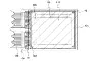
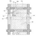
図1(A)に、本実施の形態の液晶表示装置の上面図を示す。画素電極(以下、第1の電極ともいう。)が形成された第1の基板100と対向電極(以下、第2の電極ともいう。)が形成された第2の基板102がシール材104により貼り合わされており、第1の基板100、第2の基板102、及びシール材104の内部に液晶が充填されている。第1の基板100上には、信号線駆動回路106、走査線駆動回路108、及び画素がマトリクス状に形成された表示領域110が形成されている。また、シール材104の隅には、第1の基板100に形成される接続配線114と第2の基板102に形成される対向電極とを導通する導電粒子112が設けられている。また、接続配線114は、FPC116(Flexible printed circuit)と接続される。なお、図示しないが、液晶表示装置には、光源としてバックライト、サイドライトなどが設けられる。また、第1の基板100の外側、及び第2の基板の外側それぞれには、偏光板、位相差板、反射防止板、円偏光板などが適宜設けられる。FIG. 1A shows a top view of the liquid crystal display device of this embodiment. A
ここで、モノクロ表示の画素について、図2を用いて説明する。本実施の形態に示す画素120は、信号線128の中心線と走査線130の中心線とで囲まれる領域である。画素120は、スイッチング素子124及び画素電極131を含む。また、画素の平面面積は、矢印120aで示すx方向の画素ピッチ(寸法)と、矢印120bで示すy方向の画素ピッチ(寸法)との積で求められる。Here, a monochrome display pixel will be described with reference to FIG. The
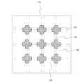
次に、図3に表示領域110の拡大図を示す。表示領域110には、画素120がマトリクス状に配置されている。さらに、各画素において、平面形状が対称性を有するスペーサ122が1つ以上設けられている。スペーサ122は、表示領域において規則的に設けられている。なお、画素120にスペーサ122が設けられる場合は、画素に設けられた画素電極の電位を制御するスイッチング素子124と重畳するように設けることで、液晶表示装置の開口率が低減しない。Next, an enlarged view of the
なお、図4に示すように、表示領域110の画素120の4隅それぞれの一部に重畳するように平面形状が対称性を有するスペーサ126が設けられてもよい。また、スペーサ126は、隣接する画素にまたがって配置される。この場合は、スペーサ126は、少なくとも信号線128及び走査線130の交差部上に設けることで、液晶表示装置の開口率の低減を妨げることができる。As shown in FIG. 4, a
図3及び図4に示す平面形状が対称性を有するスペーサ122、126の形状は、多角柱または多角錐台とすることができる。また、平面形状が対称性を有するスペーサ122、126の形状を、円柱、楕円柱、角丸多角柱、角丸多角錐台、円錐台、または楕円錐台とすることで、スペーサ122、126の平面形状が点対称であり、且つ側面が湾曲している。スペーサ122、126の側面が曲面であると、液晶の流動の妨げにならず、液晶の分布の均一性を高めることができる。なお、スペーサの平面形状における対称性は点対称に限らず、線対称でもよい。The shape of the
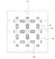
または、図5に示すように、表示領域110の画素120の4隅それぞれの一部に重畳するように平面形状が十字状であるスペーサ132が設けられてもよい。なお、図5に示す十字状のスペーサ132は、縦方向の長さと横方向の長さが異なっていてもよい。この場合は、スペーサ132は、少なくとも信号線128及び走査線130の交差部上に設けることで、液晶表示装置の開口率が低減しないと共に、セルギャップの均一性を更に高めることができる。Alternatively, as illustrated in FIG. 5, a
または、図6に示すように、表示領域110の画素120の4辺それぞれの一部に重畳するように、平面形状が対称性を有するスペーサ134が設けられてもよい。図6に示すスペーサ134は、隣接する画素の境界、即ち、走査線の中心線は信号線の中心線において線対称であることが好ましい。また、スペーサ134は、隣接する画素にまたがって配置される。この場合は、スペーサ134は、少なくとも信号線128または走査線130上に設けることで、液晶表示装置の開口率が低減しないと共に、セルギャップの均一性を更に高めることができる。Alternatively, as illustrated in FIG. 6, a
本実施の形態に示す液晶表示装置は、表示領域において、スペーサが規則的に配置されており、各画素において、少なくとも一つ以上の平面形状が対称性を有するスペーサを有する。更に、平面形状が対称性を有するスペーサの一画素における平面面積は、一画素の平面面積の13%以下、好ましくは10%以下とする。また、スペーサは各々が独立しており、隣接するスペーサと隙間を有する。このため、図3に示すように、矢印136で示す第1の方向、及び第1の方向と交差する矢印138で示す第2の方向において、スペーサ122が形成されない。このため、本実施の形態に示す液晶表示装置は、液晶注入法により第1の基板及び第2の基板の間に液晶を注入する際に、液晶が流動する領域を有し、当該領域において液晶が流動できるため、表示領域において均一性高く液晶を分布させることができる。また、液晶滴下法において第1の基板に液晶を滴下した後、第1の基板に第2の基板を封止する際、液晶が表示領域で流動することが可能であるため、表示領域において均一性高く液晶を分布させることができる。In the liquid crystal display device described in this embodiment, spacers are regularly arranged in a display region, and each pixel has a spacer having at least one planar shape that is symmetric. Further, the planar area of one pixel of the spacer having a symmetrical planar shape is 13% or less, preferably 10% or less of the planar area of one pixel. In addition, each spacer is independent and has a gap with an adjacent spacer. For this reason, as shown in FIG. 3, the
また、画素に設けられる平面形状が対称性を有するスペーサは、表示領域に規則的に配置されているため、外部からの押圧や曲げによって、第1の基板または/及び第2の基板に力が加わっても、各画素におけるセルギャップが保持されるため、液晶表示装置の表示の乱れを低減することができる。Further, since the spacers having a symmetrical planar shape provided in the pixels are regularly arranged in the display region, a force is applied to the first substrate and / or the second substrate by external pressing or bending. Even if it is added, since the cell gap in each pixel is maintained, display disturbance of the liquid crystal display device can be reduced.
更に、平面形状が対称性を有するスペーサの一画素における平面面積を、一画素の平面面積の13%以下、好ましくは10%以下とし、ブラックマトリクス、走査線、信号線、またはスイッチング素子上に設けることで、画素の開口率及び液晶の配向ムラによるコントランストの低減を妨げることが可能であり、液晶表示装置の画質を向上させることができる。Further, the plane area of one pixel of the spacer having a symmetrical plane shape is set to 13% or less, preferably 10% or less of the plane area of one pixel, and provided on the black matrix, the scanning line, the signal line, or the switching element. Thus, it is possible to prevent the reduction of contrast due to the aperture ratio of the pixel and the alignment unevenness of the liquid crystal, and the image quality of the liquid crystal display device can be improved.
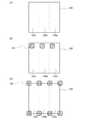
なお、図2には、モノクロ表示の液晶表示装置の画素を示したが、図7にカラー表示の液晶表示装置の画素を示す。Note that FIG. 2 shows pixels of a liquid crystal display device for monochrome display, but FIG. 7 shows pixels of a liquid crystal display device for color display.
図7(A)に示すように、カラー表示の画素120は、複数のサブ画素を有し、着色層の配置にあわせてサブ画素120c、120d、120eを有する。As shown in FIG. 7A, the
サブ画素においても、図2乃至図6に示すようにスペーサの配置とすることができる。例えば、図7(B)に示すように、サブ画素一つにおいて、スペーサ122を一つ以上配置することができる。また、図7(C)に示すように、サブ画素一つにおいて、4隅のそれぞれ一部にスペーサ122を重畳させることができる。Also in the sub-pixels, spacers can be arranged as shown in FIGS. For example, as shown in FIG. 7B, one or
なお、サブ画素の平面面積は、サブ画素のx方向におけるサブ画素ピッチと、y方向におけるサブ画素ピッチの積となる。Note that the planar area of the subpixel is the product of the subpixel pitch in the x direction of the subpixel and the subpixel pitch in the y direction.
次に、液晶表示装置の画素の構造について、図8及び図9を用いて説明する。図8及び図9においては、TN(Twisted Nematic)モードの液晶表示装置について説明する。Next, the structure of the pixel of the liquid crystal display device will be described with reference to FIGS. 8 and 9, a TN (twisted nematic) mode liquid crystal display device will be described.
図8(A)は、表示領域における一つのサブ画素120cにおいて、第1の基板側の上面図である。走査線及び信号線に接続するスイッチング素子124と、スイッチング素子124に接続する第1の電極164と、容量配線155、ゲート絶縁層(図示しない。)、及び配線160bで形成される容量素子125とを有する。容量素子125は、スイッチング素子124及び第1の電極164と電気的に接続する。また、走査線及び信号線の交差部を覆うようにスペーサ166が設けられる。なお、図8においては、図5に示すスペーサと同様の形状のスペーサ166を形成するが、図3、図4、及び図6のいずれのスペーサをも適用することができる。FIG. 8A is a top view on the first substrate side in one
図8(A)の一点破線A−Bの断面図を図9(A)に示す。第1の基板100上に、第1の電極164の電位を制御するスイッチング素子124が形成される。また、スイッチング素子124上に絶縁層160、絶縁層162が形成される。絶縁層162上に第1の電極164が形成される。スイッチング素子124と接続する配線160bと、第1の電極164とは、絶縁層160、162に設けられる開口部において接続される。絶縁層162上にスペーサ166が形成される。また、絶縁層162、第1の電極164、及びスペーサ166上に、配向膜168が形成される。A cross-sectional view taken along one-dot broken line AB in FIG. 8A is shown in FIG. A switching
第2の基板102には、スイッチング素子124への光の入射を遮断する遮光層170と、着色層172とが形成される。また、遮光層170及び着色層172上に平坦化層174が形成される。平坦化層174上に第2の電極176が形成され、第2の電極176上に配向膜178が形成される。On the
第1の基板100及び第2の基板102は、図1に示すシール材104により固定され、第1の基板100、第2の基板102、及びシール材の内側に液晶180が充填される。The
第1の電極164、液晶180、及び第2の電極176が重なり合うことで、液晶素子が形成される。The
第1の基板100及び第2の基板102としては、ガラス基板(無アルカリガラス基板とも呼ばれる。)、石英基板、セラミック基板、プラスチック基板等を適宜用いることができる。また、第1の基板100及び第2の基板102として、可撓性を有するガラス基板または可撓性を有するプラスチック基板を用いることで、可撓性を有する液晶表示装置を作製することができる。プラスチック基板としては、屈折率異方性の小さい基板を用いることが好ましく、代表的には、ポリエーテルサルフォン(PES)フィルム、ポリイミドフィルム、ポリエチレンナフタレート(PEN)フィルム、PVF(ポリビニルフルオライド)フィルム、ポリエステルフィルム、ポリカーボネート(PC)フィルム、アクリル樹脂フィルム、または半硬化した有機樹脂中に繊維体を含むプリプレグ等を用いることができる。As the
スイッチング素子124としては、ダイオード、MIM(Metal−Insulator−Metal)、バリスタなどの2端子型の能動素子、または、薄膜トランジスタなどの3端子型の能動素子を用いることができる。As the
図9(A)においては、スイッチング素子124としてボトムゲート型の薄膜トランジスタを用いて説明する。薄膜トランジスタは、ゲート電極154と、ゲート電極154上に形成されるゲート絶縁層156と、ゲート絶縁層156上に形成される半導体層158と、ソース電極及びドレイン電極として機能する配線160a、160bとを有する。なお、ゲート電極154は走査線の一部であり、ソース電極及びドレイン電極として機能する配線160aは信号線の一部である。In FIG. 9A, description is made using a bottom-gate thin film transistor as the switching
ゲート電極154は、アルミニウム、クロム、銅、タンタル、チタン、モリブデン、タングステンから選ばれた金属元素、または上述した金属元素を成分とする合金か、上述した金属元素を組み合わせた合金などを用いて形成することができる。また、マンガン、マグネシウム、ジルコニウム、ベリリウムのいずれか一または複数から選択された金属元素を用いてもよい。また、ゲート電極154は、単層構造でも、二層以上の積層構造としてもよい。The
ゲート絶縁層156は、窒化シリコン層、窒化酸化シリコン層、窒化アルミニウム層、酸化シリコン層、酸化窒化シリコン層、酸化アルミニウム層で形成する。The gate insulating layer 156 is formed using a silicon nitride layer, a silicon nitride oxide layer, an aluminum nitride layer, a silicon oxide layer, a silicon oxynitride layer, and an aluminum oxide layer.
ゲート電極154及びゲート絶縁層156は公知の手法により適宜作製することができる。The
半導体層158は、プラズマCVD法またはスパッタリング法等により形成したアモルファスシリコン、アモルファスシリコンゲルマニウム、微結晶シリコン、または微結晶シリコンゲルマニウムを用いることができる。また、半導体層158は、アモルファスシリコンまたはアモルファスシリコンゲルマニウムを加熱し、またはレーザービームを照射して結晶化したポリシリコンまたはポリシリコンゲルマニウムを用いることができる。また、半導体層158は、印刷法またはインクジェット法により形成した有機半導体を適宜用いることができる。また、半導体層158は、スパッタリング法、塗布法、印刷法、パルスレーザー蒸着法等により形成した酸化物半導体層を用いることができる。The
半導体層158に形成することが可能な酸化物半導体層は、四元系金属酸化物であるIn−Sn−Ga−Zn−O系金属酸化物や、三元系金属酸化物であるIn−Ga−Zn−O系金属酸化物、In−Sn−Zn−O系金属酸化物、In−Al−Zn−O系金属酸化物、Sn−Ga−Zn−O系金属酸化物、Al−Ga−Zn−O系金属酸化物、Sn−Al−Zn−O系金属酸化物や、二元系金属酸化物であるIn−Zn−O系金属酸化物、Sn−Zn−O系金属酸化物、Al−Zn−O系金属酸化物、Zn−Mg−O系金属酸化物、Sn−Mg−O系金属酸化物、In−Mg−O系金属酸化物などを用いることができる。ここでは、n元系金属酸化物はn種類の金属酸化物で構成される。An oxide semiconductor layer that can be formed in the
例えば、In−Ga−Zn−O系酸化物半導体とは、インジウム(In)、ガリウム(Ga)、亜鉛(Zn)を有する酸化物半導体、という意味であり、その組成比は問わない。For example, an In—Ga—Zn—O-based oxide semiconductor means an oxide semiconductor containing indium (In), gallium (Ga), and zinc (Zn), and there is no limitation on the composition ratio.
また、酸化物半導体層は、化学式InMO3(ZnO)m(m>0)で表記される薄膜を用いることができる。ここで、Mは、Zn、Ga、Al、Mn及びCoから選ばれた一または複数の金属元素を示す。例えばMとして、Ga、Ga及びAl、Ga及びMn、またはGa及びCoなどがある。As the oxide semiconductor layer, a thin film represented by the chemical formula, InMO3 (ZnO)m (m> 0) can be used. Here, M represents one or more metal elements selected from Zn, Ga, Al, Mn, and Co. For example, M includes Ga, Ga and Al, Ga and Mn, or Ga and Co.
また、酸化物半導体としてIn−Zn−O系の材料を用いる場合、用いるターゲットの組成比は、原子数比で、In:Zn=50:1〜1:2(モル数比に換算するとIn2O3:ZnO=25:1〜1:4)、好ましくはIn:Zn=20:1〜1:1(モル数比に換算するとIn2O3:ZnO=10:1〜1:2)、さらに好ましくはIn:Zn=15:1〜1.5:1(モル数比に換算するとIn2O3:ZnO=15:2〜3:4)とする。例えば、In−Zn−O系酸化物半導体の形成に用いるターゲットは、原子数比がIn:Zn:O=X:Y:Zのとき、Z>1.5X+Yとする。In the case where an In—Zn—O-based material is used as the oxide semiconductor, the composition ratio of the target used is an atomic ratio, and In: Zn = 50: 1 to 1: 2 (in terms of the molar ratio, In2 O3 : ZnO = 25: 1 to 1: 4), preferably In: Zn = 20: 1 to 1: 1 (In2 O3 : ZnO = 10: 1 to 1: 2 in terms of molar ratio), More preferably, In: Zn = 15: 1 to 1.5: 1 (In2 O3 : ZnO = 15: 2 to 3: 4 in terms of molar ratio). For example, a target used for forming an In—Zn—O-based oxide semiconductor satisfies Z> 1.5X + Y when the atomic ratio is In: Zn: O = X: Y: Z.
なお、酸化物半導体層には、不純物として、主成分とする金属酸化物以外の元素が1%、好ましくは0.1%入ってもよい。半導体層158に形成することが可能な金属酸化物は、エネルギーギャップが2eV以上、好ましくは2.5eV以上、より好ましくは3eV以上である。Note that the oxide semiconductor layer may contain 1%, preferably 0.1%, of an element other than the metal oxide as a main component as impurities. The metal oxide that can be formed in the
さらに、酸化物半導体層は、i型化または実質的にi型化された酸化物半導体層で形成してもよい。i型化または実質的にi型化された酸化物半導体層は、キャリア密度が5×10¹⁴/cm3未満、好ましくは1×1012/cm3未満、より好ましくは1×1011/cm3以下である。また、ドナーとして寄与する水素や酸素欠陥は少ないことが好ましく、水素濃度が1×1016/cm3以下が好ましい。なお、キャリア密度は、ホール効果測定により得られる。また、より低濃度のキャリア密度の測定は、CV測定(Capacitance−Voltage−Measurement)の測定結果により得られる。また、酸化物半導体層中の水素濃度測定は、二次イオン質量分析法(SIMS:Secondary Ion Mass Spectroscopy)により得られる。Further, the oxide semiconductor layer may be an i-type or substantially i-type oxide semiconductor layer. The i-type or substantially i-type oxide semiconductor layer has a carrier density of less than 5 × 10¹⁴ / cm3 , preferably less than 1 × 10¹² / cm3 , more preferably 1 × 10¹¹ / cm 3.3 or less. Moreover, it is preferable that there are few hydrogen and oxygen defects which contribute as a donor, and hydrogen concentration is 1 * 10 <16 > / cm <3 > or less. The carrier density is obtained by measuring the Hall effect. Moreover, the measurement of the carrier density of a lower density | concentration is obtained from the measurement result of CV measurement (Capacitance-Voltage-Measurement). In addition, measurement of the hydrogen concentration in the oxide semiconductor layer is obtained by secondary ion mass spectrometry (SIMS).
i型化または実質的にi型化された酸化物半導体層をチャネル領域に用いた薄膜トランジスタは、オフ電流が1×10⁻¹⁹A/μm以下、さらには1×10−20A/μm以下と低くすることができる。これは、i型化または実質的にi型化された酸化物半導体層は、バンドギャップが広く、電子の励起のために大きな熱エネルギーが必要であるため、直接再結合及び間接再結合が生じにくい。このため、ゲート電極に負の電位が印加された状態(オフ状態)では、少数キャリアであるホールは実質的にゼロであるため、直接再結合及び間接再結合が生じにくく、電流は限りなく低くなる。この結果、薄膜トランジスタのオフ状態において、酸化物半導体層は絶縁体とみなせて回路設計を行うことができる。一方で、i型化または実質的にi型化された酸化物半導体層は、薄膜トランジスタの導通状態(オン状態)においては、非晶質シリコンで形成される半導体層よりも高い電流供給能力を見込むことができる。このため、薄膜トランジスタは、オフ状態では極めてリーク電流の低いノーマリーオフ状態となり、優れたスイッチング特性を有する。A thin film transistor in which an i-type or substantially i-type oxide semiconductor layer is used for a channel region has an off-state current of 1 × 10⁻¹⁹ A / μm or less, further 1 × 10⁻²⁰ A / μm or less. Can be lowered. This is because an i-type or substantially i-type oxide semiconductor layer has a wide band gap and requires large thermal energy for excitation of electrons, so that direct recombination and indirect recombination occur. Hateful. For this reason, in a state where a negative potential is applied to the gate electrode (off state), since holes that are minority carriers are substantially zero, direct recombination and indirect recombination hardly occur, and the current is extremely low. Become. As a result, in the off state of the thin film transistor, the oxide semiconductor layer can be regarded as an insulator and circuit design can be performed. On the other hand, an i-type or substantially i-type oxide semiconductor layer expects a higher current supply capability than a semiconductor layer formed using amorphous silicon in a conductive state (on state) of a thin film transistor. be able to. Therefore, the thin film transistor is in a normally-off state with extremely low leakage current in the off state, and has excellent switching characteristics.
なお、図9(A)に示す薄膜トランジスタおいて、半導体層158上に配線160a、160bを形成したが、ゲート絶縁層156及び半導体層158の間に配線160a、160bを形成してもよい。さらには、薄膜トランジスタをトップゲート型の薄膜トランジスタとすることもできる。この場合は、半導体層158で列挙した材料の他、単結晶シリコン層を用いることができる。なお、単結晶シリコン層をチャネル領域に用いたトランジスタとしては、単結晶シリコン基板をチャネル領域に用いたトランジスタの他、絶縁領域上に単結晶シリコン層が形成される、いわゆるSOI(Silicon on Insulator)基板をチャネル領域に用いたトランジスタを用いることができる。Note that in the thin film transistor illustrated in FIG. 9A, the
絶縁層160は、ゲート絶縁層156と同様の材料及び作製方法適宜を用いて形成することができる。The insulating
絶縁層162は、有機樹脂層を塗布法または印刷法により用いて形成することができる。有機樹脂層としては、例えばアクリル、エポキシ、ポリイミド、ポリアミド、ポリビニルフェノール、ベンゾシクロブテンなどを用いることができる。また、シロキサンポリマーを用いることができる。The insulating
第1の電極164は、透過型の液晶表示装置の場合と反射型の液晶表示装置で異なる。透過型液晶表示装置の場合、第1の電極164は、透光性を有する材料を用いて形成する。透光性を有する材料とは、酸化インジウムスズ(ITO)、酸化亜鉛(ZnO)、酸化インジウム亜鉛(IZO)、ガリウムを添加した酸化亜鉛(GZO)等がある。The
また、第1の電極164として、導電性高分子(導電性ポリマーともいう)を含む導電性組成物を用いて形成することができる。導電性組成物を用いて形成した画素電極は、シート抵抗が10000Ω/□以下、波長550nmにおける透光率が70%以上であることが好ましい。また、導電性組成物に含まれる導電性高分子の抵抗率が0.1Ω・cm以下であることが好ましい。Alternatively, the
導電性高分子としては、いわゆるπ電子共役系導電性高分子が用いることができる。例えば、ポリアニリンまたはその誘導体、ポリピロールまたはその誘導体、ポリチオフェンまたはその誘導体、若しくはこれらの2種以上の共重合体などがあげられる。As the conductive polymer, a so-called π-electron conjugated conductive polymer can be used. For example, polyaniline or a derivative thereof, polypyrrole or a derivative thereof, polythiophene or a derivative thereof, or a copolymer of two or more kinds thereof can be given.
反射型の液晶表示装置の場合、第1の電極164は反射率の高い金属電極を用いて形成する。代表的には、アルミニウム、銀等が用いられる。また、第1の電極164の表面を凹凸状にすることで、反射率を高めると共に、写りこみを低減することができる。このため、反射型液晶表示装置の場合は、第1の電極164の下地膜である絶縁層162を凹凸とすることが好ましい。In the case of a reflective liquid crystal display device, the
また、半透過型の液晶表示装置の場合には、画素電極は透過型の材料と反射型の材料が用いられる。In the case of a transflective liquid crystal display device, a transmissive material and a reflective material are used for the pixel electrode.
第1の電極164は、印刷法、インクジェット法、スパッタリング法、CVD法、蒸着法等により形成することができる。The
スペーサ166は、第1の基板100及び第2の基板102の間隔を保持するためのものである。スペーサ166は、本実施の形態では、フォトリソグラフィ工程により所定の場所に形成するものであり、代表的には、フォトリソスペーサー、ポストスペーサー、貝柱スペーサ、カラムスペーサー、柱状スペーサとも呼ばれている。基板の全面に、アクリル、ポリイミドなどの感光性有機樹脂層をスピンコート法または印刷法により形成した後、フォトリソグラフィ工程を行うことにより、基板上に感光性の有機樹脂層を形成することができ、当該感光性の有機樹脂層がスペーサとして機能する。当該方法により、露光時のマスクパターン次第でスペーサの配置したい場所に露光できるため、走査線、信号線、スイッチング素子等と重畳するようにスペーサを配置することが可能であり、第1の基板100及び第2の基板102の間隔を保持するだけでなく、液晶の光漏れ及び開口率の低減も防ぐことができる。また、スペーサ166は、インクジェット法により有機絶縁材料を含む組成物を吐出し焼成して形成することができる。The
配向膜168はラビング処理または光配向処理によって形成することができる。なお、ブルーモード液晶表示装置や高分子分散型液晶表示装置等においては、配向膜を形成しない場合もある。また、垂直配向モードの液晶表示装置においては、配向膜を形成する代わりに、第1の電極または第2の電極にスリットを形成する、または第1の電極または第2の電極上に誘電体を形成する等の工程により、配向膜を設けずとも、液晶にプレチルト状態に保持することができる。The
第2の基板102は、第1の基板100と同様の基板を適宜用いることができる。As the
着色層172は、可視光の波長範囲のうち、任意の波長範囲の光を優先的に透過させる機能を有する。通常は、赤色波長範囲の光、青色波長範囲の光、及び緑色波長範囲の光、それぞれを優先的に透過させる着色層を組み合わせて、カラーフィルタとして機能させることができる。しかしながら、着色層の組み合わせに関しては、これに限られない。赤色波長の範囲の光、青色波長範囲の光、及び緑色波長範囲の光に加えて、白色波長範囲の光を優先的に透過させる着色層を組み合わせることで、液晶表示装置の輝度を高めることができる。または、白色波長範囲の光の代わりに、イエロー、シアン、マゼンタ等の波長範囲の光を優先的に透過させる着色層を一つ以上追加することができる。なお、各色要素ごとにサブ画素の面積が異なっていてもよい。The
遮光層170及び着色層172は、顔料が分散された感光性樹脂を用いたエッチング法、カラーレジストを用いたカラーレジスト法、染色法、電着法、ミセル電解法、電着転写法、フィルム分散法、インクジェット法(液滴吐出法)、銀塩発色法など公知の手法を用いての形成することができる。The
本実施の形態では、顔料が分散された感光性樹脂を用いたエッチング法によって、遮光層170及び着色層172を形成する。はじめに、黒色顔料が分散された感光性アクリル樹脂材料を塗布法により第2の基板102上に塗布する。次に、アクリル樹脂材料を乾燥し、仮焼きした後、露光及び現像し、加熱してアクリル樹脂材料を硬化し、遮光層170を形成する。次に、赤色顔料、緑色顔料、または青色顔料が分散された感光性アクリル樹脂材料をそれぞれ塗布し、遮光層170と同様の工程によって、それぞれ赤色着色層、緑色着色層、青色着色層を形成する。この後、有機樹脂材料を塗布し平坦化層174を形成する。In this embodiment mode, the
第2の電極176は、第1の電極164に示す透光性を有する材料を適宜用いることができる。The
配向膜178は、配向膜168と同様に形成することができる。The
液晶180は、サーモトロピック液晶、低分子液晶、高分子液晶、高分子分散型液晶、強誘電性液晶、反強誘電性液晶等を用いる。As the
また、液晶180は、カイラル剤光硬化樹脂が混合されたブルー相を示す液晶を用いることができる。ブルー相を示す液晶としては、サーモトロピック液晶、低分子液晶、高分子液晶、強誘電性液晶、反強誘電性液晶等がある。カイラル剤は、液晶を螺旋構造に配向させ、ブルー相を発現させるために用いる。一例として、カイラル剤を混合させることで、サーモトロピック液晶、低分子液晶、高分子液晶、強誘電性液晶、反強誘電性液晶がブルー相を示すことができる。カイラル剤が混合されたブルー相を示す液晶は、応答速度が1msec以下と短く、光学的等方性であるため、視野角依存性が小さい。As the
図9(B)に、図9(A)とは異なる液晶表示装置の断面構造を示す。ここでは、第2の基板102側に着色層が形成されず、第1の基板100側に着色層が形成されることを特徴とする。また、スペーサ167が、第2の基板102上に形成されることを特徴とする。FIG. 9B illustrates a cross-sectional structure of a liquid crystal display device, which is different from that in FIG. Here, a colored layer is not formed on the
第1の基板100上に、スイッチング素子124が形成される。A switching
スイッチング素子124上に形成される絶縁層160上に、着色層182が形成される。着色層182上に、着色層182に含まれる不純物が液晶180に混入するのを防ぐために、保護層184が形成される。保護層184上に、第1の電極164が形成される。着色層182は、画素毎に、任意の波長範囲の光(赤色、青色、または緑色)を優先的に透過させる層で形成すればよい。また、着色層182は平坦化層としても機能するため、液晶180の配向ムラ、光漏れ、ディスクリネーション等を低減することができる。A
スイッチング素子124の配線160bと、第1の電極164とは、絶縁層160、着色層182、及び保護層184に設けられる開口部において接続される。第1の電極164上には配向膜169が形成される。The
第2の基板102には、スイッチング素子124への光の入射を遮断する遮光層170と、遮光層170及び第2の基板102を覆う平坦化層174が形成される。平坦化層174上に第2の電極176が形成され、第2の電極176上にスペーサ167が形成される。第2の電極176およびスペーサ167上に配向膜179が形成される。The
第1の電極164、液晶180、及び第2の電極176が重なり合うことで、液晶素子が形成される。The
図9(B)に示す液晶表示装置は、遮光層170と、着色層182を同一基板上に形成しない。このため、着色層182の形成工程におけるマスクずれを回避するため、遮光層170の面積を大きくする必要がなくなり、画素における開口率を向上させることができる。In the liquid crystal display device illustrated in FIG. 9B, the light-
なお、図9(A)においては、スペーサ166は第1の基板100上に形成されるが、図9(B)に示すように第2の基板102に形成することができる。また、図9(B)においては、スペーサ167は第2の基板102上に形成されるが、図9(B)に示すように第1の基板100に形成することができる。9A, the
また、図9においては、液晶表示装置として、TNモードの液晶表示装置を示したが、これに限定されない。すなわち、FFS(Fringe Field Switching)モード、IPS(In−Plane−Switching)モード、OCB(Optical Compensated Birefringence)モード、FLC(Ferroelectric Liquid Crystal)モード、AFLC(AntiFerroelectric Liquid Crystal)モード、垂直配向(VA)モード、またはその他の液晶表示装置とすることができる。垂直配向(VA)モードとしては、例えば、MVA(Multi−Domain Vertical Alignment)モード、PVA(Patterned Vertical Alignment)モード、ASM(Axially Symmetric aligned Micro−cellなどを用いることができる。具体的には、1画素を複数のサブ画素に分割し、各サブ画素の中央に位置する対向基板の箇所に凸部を設けることで1画素をマルチドメイン化する。なお、凸部は、第1の基板または第2の基板の一方または両方に設けてもよく、放射状に液晶分子を配向させ、配向規制力を向上させる。なお、IPS型の液晶表示装置は、横電界で液晶の配向を制御するため、第2の電極が第1の電極と同様に第1の基板100上に形成される。Although FIG. 9 shows a TN mode liquid crystal display device as the liquid crystal display device, the present invention is not limited to this. That is, FFS (Fringe Field Switching) mode, IPS (In-Plane-Switching) mode, OCB (Optical Compensated Birefringence) mode, FLC (Ferroelectric Liquid Crystal) mode, AFLC (AntificFrequency AristFrequency) Or other liquid crystal display devices. As the vertical alignment (VA) mode, for example, MVA (Multi-Domain Vertical Alignment) mode, PVA (Patterned Vertical Alignment) mode, ASM (Axial Symmetrical Aligned Micro-cell), and the like can be used. The pixel is divided into a plurality of sub-pixels, and a convex portion is provided at the position of the counter substrate located at the center of each sub-pixel, so that one pixel is multi-domained. It may be provided on one or both of the substrates, and the liquid crystal molecules are aligned radially to improve the alignment regulation power. Of the
図1に示すシール材104は、可視光硬化性、紫外線硬化性または熱硬化性の樹脂を含む材料を用いることができる。例えば、ビスフェノールA型液状樹脂、ビスフェノールA型固形樹脂、含ブロムエポキシ樹脂、ビスフェノールF型樹脂、ビスフェノールAD型樹脂、フェノール型樹脂、クレゾール型樹脂、ノボラック型樹脂、環状脂肪族エポキシ樹脂、エピビス型エポキシ樹脂、グリシジルエステル樹脂、グリジシルアミン樹脂、複素環式エポキシ樹脂、変性エポキシ樹脂等のエポキシ樹脂を用いることができる。シール材104は、スクリーン印刷法、インクジェット装置またはディスペンス装置を用いて第1の基板100または第2の基板102上に塗布する。なお、シール材104に、第1の基板100及び第2の基板102の間隔を保つためのフィラー(直径1μm〜24μm)を含んでもよい。As the
導電粒子112は、絶縁性球体に金属層が被覆された導電粒子を用いることができる。絶縁性球体は、シリカガラス、硬質樹脂等で形成される。金属層は、金、銀、パラジウム、ニッケル、ITO、及びIZOの単層または積層構造とすることができる。As the
次に、図9に示す液晶表示装置の作製方法について、説明する。第1の基板100または第2の基板102上にシール材104を設けた後、第1の基板100及び第2の基板102の位置合わせをする。次に、可視光照射、紫外光照射、または加熱処理によりシール材104を硬化して第1の基板100及び第2の基板102を貼り合せる。Next, a method for manufacturing the liquid crystal display device illustrated in FIG. 9 is described. After the
次に、液晶注入法により、第1の基板100、第2の基板102、及びシール材104内に液晶を充填させる。この後、液晶の注入口に封止材を設けることで、液晶表示装置を作製することできる。Next, liquid crystal is filled into the
または、第1の基板100または第2の基板102上にシール材104を設け、第1の基板100または第2の基板102に液晶滴下法により液晶を滴下した後、第1の基板100及び第2の基板102の位置合わせをする。次に、可視光照射、紫外光照射、または加熱処理によりシール材104を硬化して、第1の基板100及び第2の基板102を貼り合せることで、液晶表示装置を作製することできる。Alternatively, after the
本実施の形態に示す液晶表示装置は、表示領域においてスペーサが規則的に配置され、各画素において、少なくとも一つ以上の平面形状が対称性を有するスペーサを有する。更に、平面形状が対称性を有するスペーサの一画素における平面面積は、一画素の平面面積の13%以下、好ましくは10%以下とする。また、スペーサは各々が独立しており、隣接するスペーサと隙間を有する。このため、液晶注入法により第1の基板及び第2の基板の間に液晶を注入する際に、液晶の流動領域を形成することが可能であり、当該領域において液晶が流動するため、表示領域において均一性高く液晶を分布させることができる。また、液晶滴下法において第1の基板に液晶を滴下した後、第1の基板に第2の基板を封止する際、液晶が表示領域で流動することが可能であるため、表示領域において均一性高く液晶を分布させることができる。In the liquid crystal display device described in this embodiment, spacers are regularly arranged in a display region, and each pixel has a spacer having at least one planar shape that is symmetric. Further, the planar area of one pixel of the spacer having a symmetrical planar shape is 13% or less, preferably 10% or less of the planar area of one pixel. In addition, each spacer is independent and has a gap with an adjacent spacer. Therefore, when the liquid crystal is injected between the first substrate and the second substrate by the liquid crystal injection method, a liquid crystal flow region can be formed, and the liquid crystal flows in the region. The liquid crystal can be distributed with high uniformity. Further, after the liquid crystal is dropped on the first substrate in the liquid crystal dropping method, the liquid crystal can flow in the display region when the second substrate is sealed to the first substrate. Liquid crystal can be distributed with high performance.
また、画素に設けられる平面形状が対称性を有するスペーサは、規則的に表示領域に配置されているため、外部からの押圧や曲げによって、第1の基板または/及び第2の基板に力が加わっても、各画素におけるセルギャップが保持されるため、液晶表示装置の表示の乱れを低減することができる。In addition, since the planar shape provided in the pixel is symmetrical in the display area, the spacer is regularly arranged in the display region. Therefore, a force is applied to the first substrate and / or the second substrate by external pressing or bending. Even if it is added, since the cell gap in each pixel is maintained, display disturbance of the liquid crystal display device can be reduced.
更に、平面形状が対称性を有するスペーサの一画素における平面面積を、一画素の平面面積の13%以下、好ましくは10%以下とし、遮光層、走査線、信号線、またはスイッチング素子上に設けることで、画素の開口率及び液晶の配向ムラによるコントランストの低減を妨げることが可能であり、液晶表示装置の画質を向上させることができる。Further, the planar area of one pixel of the spacer having a symmetrical planar shape is set to 13% or less, preferably 10% or less of the planar area of one pixel, and is provided on the light shielding layer, the scanning line, the signal line, or the switching element. Thus, it is possible to prevent the reduction of contrast due to the aperture ratio of the pixel and the alignment unevenness of the liquid crystal, and the image quality of the liquid crystal display device can be improved.
また、本実施の形態では、液晶表示装置として、走査線駆動回路及び信号線駆動回路が第1の基板上に設けられているが、走査線駆動回路及び信号線駆動回路の一方または両方をFPC上に設けてもよい。In this embodiment, as the liquid crystal display device, the scan line driver circuit and the signal line driver circuit are provided over the first substrate; however, one or both of the scan line driver circuit and the signal line driver circuit are FPCs. It may be provided above.
また、液晶表示装置は、FPCの代わりに、TAB(Tape Automated Bonding)テープもしくはTCP(Tape Carrier Package)が取り付けられたモジュール、TABテープやTCPの先にプリント配線板が設けられたモジュールも全て液晶表示装置に含むものとする。更には、FPC、TAB、TCP等のコネクターが設けられていないものも液晶表示装置に含むものとする。In addition, the liquid crystal display device is not limited to the FPC, but a module in which a TAB (Tape Automated Bonding) tape or TCP (Tape Carrier Package) is attached, and a module in which a printed wiring board is provided on the end of the TAB tape or TCP are all liquid crystals. It shall be included in the display device. Furthermore, liquid crystal display devices include those not provided with connectors such as FPC, TAB, and TCP.
また、カラー表示をフィールドシーケンシャルと言われる色順次方式で表示する場合には着色層を設けなくともよい。Further, when the color display is displayed by a color sequential method called field sequential, a colored layer is not necessarily provided.
また、本実施の形態に示す液晶表示装置のスペーサの配置は、表示領域において規則的であればよく、走査線駆動回路、信号線駆動回路その他の非表示領域においては、スペーサの配置はランダムでも規則的でもよい。In addition, the arrangement of the spacers in the liquid crystal display device described in this embodiment mode may be regular in the display area. In the scanning line driver circuit, the signal line driver circuit, and other non-display areas, the spacers may be arranged randomly. It may be regular.
なお、本実施の形態では、画素にスイッチング素子を有するアクティブマトリクス型の液晶表示装置を示したが、パッシブマトリクス型の液晶表示装置に上記スペーサを設けることができる。パッシブマトリクス型の液晶表示装置は、図10に示すように、第1の方向に一定間隔の隙間をあけて配置される第1の電極192と、一定間隔の隙間をあけて第1の方向と交差する方向に配置される第2の電極194が、少なくとも液晶を介して重畳する。また、画素190は、第1の電極192の隙間の中心線と、第2の電極194の隙間の中心線で囲まれる領域である。画素190の平面面積は、矢印190aで示すx方向の画素ピッチ(寸法)と、矢印190bで示すy方向の画素ピッチ(寸法)との積で求められる。Note that although an active matrix liquid crystal display device including a switching element in a pixel is described in this embodiment mode, the spacer can be provided in a passive matrix liquid crystal display device. As shown in FIG. 10, the passive matrix type liquid crystal display device includes a
パッシブマトリクス型の液晶表示装置においても、図3乃至図6に示すようなスペーサを配置することができる。Also in the passive matrix liquid crystal display device, spacers as shown in FIGS. 3 to 6 can be provided.
(実施の形態2)
本実施の形態では、外部からの押圧や曲げによる表示の乱れが少なく、且つ機械強度の高い液晶表示装置について、図1及び図11を用いて説明する。(Embodiment 2)
In this embodiment, a liquid crystal display device with less display disturbance due to external pressing or bending and high mechanical strength will be described with reference to FIGS.
図11は、図1に示す表示領域110の拡大図である。表示領域には、画素120がマトリクス状に配置されている。また、表示領域110においてスペーサが規則的に配置されており、各画素において、平面形状が対称性を有するスペーサが1つ以上設けられている。当該スペーサは、第1の基板及び第2の基板の間隔を保持するスペーサ122と、粘着性を有し、第1の基板及び第2の基板の密着性を高めるスペーサ140の2種類あり、これらが交互に設けられている。図11においては、図4と同様に、画素120の4隅それぞれの一部に重畳するようにスペーサ122、スペーサ140が交互に設けられているが、図3、図5、及び図6のスペーサの配置位置及び形状を適宜適用することができる。FIG. 11 is an enlarged view of the
粘着性を有し、第1の基板及び第2の基板の密着性を高めるスペーサ140は、実施の形態1に示すシール材104の材料を適宜用いて形成することができる。The
粘着性を有するスペーサ140は、第1の基板または第2の基板上に、第1の基板及び第2の基板の間隔を保持するスペーサ122を形成した後、シール材104を描画すると共に、粘着性を有するスペーサ140を表示領域110に形成すればよい。次に、第1の基板及び第2の基板の位置合わせをした後、可視光照射、紫外光照射、または加熱処理によりシール材104及び粘着性を有するスペーサ140を硬化して、第1の基板及び第2の基板を貼り合せる。次に、液晶注入法により、第1の基板、第2の基板、及びシール材内に液晶を充填させる。この後、液晶の注入口に封止材を設けることで、液晶表示装置を作製することできる。The
または、粘着性を有するスペーサ140は、第1の基板または第2の基板上に、第1の基板及び第2の基板の間隔を保持するスペーサ122を形成した後、シール材104を描画すると共に、粘着性を有するスペーサ140を表示領域110に形成すればよい。次に、第1の基板または第2の基板上にシール材を設け、液晶滴下法により液晶を滴下する。次に、第1の基板及び第2の基板の位置合わせをした後、可視光照射、紫外光照射、または加熱処理によりシール材及び粘着性を有するスペーサ140を硬化して、第1の基板及び第2の基板を貼り合せることで、液晶表示装置を作製することできる。Alternatively, the
本実施の形態に示す液晶表示装置は、各画素において、少なくとも一つ以上の平面形状が対称性を有するスペーサを有する。当該スペーサは、第1の基板及び第2の基板の間隔を保持するスペーサと、第1の基板及び第2の基板の密着性を高めるスペーサとが、交互に設けられている。更に、一画素におけるスペーサの平面面積は、一画素の平面面積の13%以下、好ましくは10%以下とする。The liquid crystal display device described in this embodiment includes a spacer in which at least one planar shape is symmetric in each pixel. As the spacer, a spacer that keeps a distance between the first substrate and the second substrate and a spacer that improves the adhesion between the first substrate and the second substrate are alternately provided. Furthermore, the planar area of the spacer in one pixel is 13% or less, preferably 10% or less of the planar area of one pixel.
各画素にスペーサが設けられているため、表示領域において均一性高く液晶を分布させることができるため、外部からの押圧や曲げによって、第1の基板または/及び第2の基板に力が加わっても、各画素におけるセルギャップが保持されるため、液晶表示装置の表示の乱れを低減することができる。Since each pixel is provided with a spacer, the liquid crystal can be distributed with high uniformity in the display region. Therefore, force is applied to the first substrate and / or the second substrate by external pressure or bending. In addition, since the cell gap in each pixel is maintained, the display disorder of the liquid crystal display device can be reduced.
更に、第1の基板及び第2の基板の間隔を保持するスペーサと、第1の基板及び第2の基板の密着性を高めるスペーサとが、交互に設けられており、第1の基板及び第2の基板の密着性が高められ、且つ、第1の基板及び第2の基板の間隔の分布を高めることが可能であるため、液晶表示装置の機械強度を高めるとともに、表示の乱れを低減することができる。Furthermore, a spacer for maintaining a distance between the first substrate and the second substrate and a spacer for improving the adhesion between the first substrate and the second substrate are alternately provided. The adhesion between the two substrates can be improved, and the distribution of the distance between the first substrate and the second substrate can be increased, so that the mechanical strength of the liquid crystal display device is increased and display disturbance is reduced. be able to.
(実施の形態3)
本実施の形態では、外部からの押圧や曲げによる表示の乱れが少ないタッチパネルについて、図12を用いて説明する。(Embodiment 3)
In this embodiment, a touch panel with less display disturbance due to external pressing or bending will be described with reference to FIGS.
図12は、タッチセンサを有する液晶表示装置の表示領域の断面図である。第2の基板102上に、タッチセンサ部270が設けられる。タッチセンサ部270は、抵抗膜方式、表面型静電容量方式、投影型静電容量方式等を適宜用いることができる。本実施の形態では、タッチセンサ部270として、抵抗膜方式のタッチセンサを用いた形態について説明する。FIG. 12 is a cross-sectional view of a display area of a liquid crystal display device having a touch sensor. A
タッチセンサ部270は、第3の基板280上に形成された第3の電極282と、第4の基板284上に形成された第4の電極286で構成される。第3の基板280上には、第3の電極282及びスペーサ288が形成される。また、第4の基板284及び第3の基板280がシール材(図示しない。)で封止される。なお、図示しないが、第1の基板100の外側と、第2の基板102及び第3の基板280との間には、それぞれ偏光板、位相差板、反射防止板、円偏光板などが適宜設けられる。The
第3の基板280及び第4の基板284は、第1の基板100と同様の基板を用いることができる。また、第3の電極282及び第4の電極286は、第1の電極164に示す透光性を有する材料を適宜用いて形成することができる。As the
外部から所定の位置をペンまたは指で押圧すると、少なくとも第4の基板284が変形し、第3の電極282及び第4の電極286が接触することで電気が流れる。当該電気抵抗の変化により、押圧された位置情報を検出することが可能である。また、本実施の形態に示す液晶表示装置は、各画素に一つ以上のスペーサを有するため、外部から所定の位置をペンまたは指で押圧されても、各画素におけるセルギャップを保つことができるため、液晶表示装置の表示乱れを低減することができる。When a predetermined position is pressed from the outside with a pen or a finger, at least the
なお、本実施の形態は、他の実施の形態と適宜組み合わせることができる。Note that this embodiment can be combined with any of the other embodiments as appropriate.
(実施の形態4)
本実施の形態では、可撓性を有する液晶表示装置を歩留まり高く作製する方法を提供することを目的とする。(Embodiment 4)
An object of this embodiment is to provide a method for manufacturing a flexible liquid crystal display device with high yield.
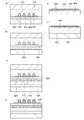
図13(A)に示すように、基板400の一表面に剥離層402を形成し、剥離層402上に素子層404を形成する。素子層404は剥離層402に接する絶縁層と、絶縁層上に形成され、画素電極として機能する第1の電極に印加する電圧を制御するスイッチング素子と、スイッチング素子を覆う絶縁層とを少なくとも有する。スイッチング素子は、実施の形態1に示すスイッチング素子124を適宜作製することができる。As shown in FIG. 13A, a
素子層404上に第1の電極406を形成し、第1の電極406上にスペーサ408を形成する。A
基板400は、ガラス基板、石英基板、金属基板やステンレス基板等を用いるとよい。例えば、1辺が1メートル以上の矩形状のガラス基板を用いることにより、生産性を格段に向上させることができる。As the
なお、本工程では、剥離層402を基板400の全面に設ける場合を示しているが、必要に応じて、基板400の全面に剥離層402を設けた後に当該剥離層402を選択的に除去し、所望の領域にのみ剥離層を設けてもよい。また、基板400に接して剥離層402を形成しているが、必要に応じて、基板400に接するように酸化シリコン層、酸化窒化シリコン層、窒化シリコン層、窒化酸化シリコン層等の絶縁層を形成し、当該絶縁層に接するように剥離層402を形成してもよい。Note that although the case where the
剥離層402は、スパッタリング法やプラズマCVD法、塗布法、印刷法等により、厚さ30nm〜200nmのタングステン(W)、チタン(Ti)、タンタル(Ta)、ニオブ(Nb)、ニッケル(Ni)、コバルト(Co)、ジルコニウム(Zr)、亜鉛(Zn)、及びシリコン(Si)の中から選択された元素、または元素を主成分とする合金材料、または元素を主成分とする化合物材料からなる層を、単層または複数の層を積層させて形成する。シリコン層の結晶構造は、非晶質、微結晶、多結晶のいずれの場合でもよい。The
剥離層402が積層構造の場合、好ましくは、1層目として金属層を形成し、2層目として金属酸化物層を形成する。代表的には、1層目の金属層として、タングステン、またはタングステンとモリブデンの混合物を含む層を形成し、2層目として、タングステン、またはタングステンとモリブデンとの混合物の酸化物、タングステン、またはタングステンとモリブデンとの混合物の窒化物、タングステン、またはタングステンとモリブデンとの混合物の酸化窒化物、もしくはタングステン、またはタングステンとモリブデンとの混合物の窒化酸化物を含む層を形成する。なお、2層目として金属酸化物層を形成する場合、1層目の金属層の表面を、熱酸化処理、酸素プラズマ処理、オゾン水等の酸化力の強い溶液での処理等を行って金属酸化物層を形成してもよい。In the case where the
第1の電極406は、実施の形態1に示す第1の電極164と同様に形成することができる。The
スペーサ408は、実施の形態1に示すスペーサ166と同様に形成することができる。The
次に、素子層404を基板400から容易に剥離するために、素子層404にレーザービームを照射して、剥離層402が露出する凹部を形成することが好ましい。ここでは、素子層404の端部にレーザービームを照射することにより凹部を形成する(図示しない。)。Next, in order to easily peel the
次に、素子層404、第1の電極406、及びスペーサ408上に、剥離可能な有機樹脂層412を形成した後、有機樹脂層412上に粘着層を有するフィルム414を形成する。剥離可能な有機樹脂層412は、紫外線により剥離する紫外線剥離型有機樹脂、熱により剥離する熱剥離型有機樹脂、水溶性有機樹脂等がある。粘着層を有するフィルム414としては、紫外線硬化型粘着フィルム(UVフィルム、UVテープ、UVシートともいう。)、圧力が加わることにより粘着力が変化する感圧フィルム(感圧フィルム、感圧テープ、感圧シートともいう。)、熱硬化型粘着フィルム(熱硬化型粘着テープ、熱硬化型粘着シートともいう。)等がある。Next, after a peelable
粘着層を有するフィルム414を貼り合わせることにより、剥離が容易に行えると共に剥離の前後において素子層404に加わる応力を低減し、素子層404に含まれるスイッチング素子の破損を抑制することが可能となる。By laminating the
次に、図13(B)に示すように、剥離層402及び素子層404の界面において、素子層404を基板400から剥離する。剥離方法としては、例えば、機械的な力を加えること(人間の手、把治具等で引き剥がす処理や、ローラーを回転させながら分離する処理等)を用いて行えばよい。Next, as illustrated in FIG. 13B, the
なお、粘着層を有するフィルム414側を吸着ステージで吸着しながら、機械的な力を剥離層402及び素子層404の界面に加えることで、素子層404へのダメージを低減しつつ、剥離することが可能である。また、当該剥離工程の前に、剥離層402及び素子層404界面に液体(代表的には水)を供給することで、毛細管現象により剥離工程を容易に行うことができる。The
または、上記剥離工程の代わりに、NF3、BrF3、ClF3等のフッ化ガスにより剥離層をエッチングし除去して、基板400から素子層404を剥離する方法を用いることができる。または、上記剥離工程の代わりに、基板400として透光性を有する基板を用い、剥離層402として水素を含む非晶質シリコン層を用い、基板400から剥離層402にレーザービームを照射して、非晶質シリコン層に含まれる水素を気化させて、基板400と剥離層402との間で剥離する方法を用いることができる。Alternatively, instead of the above-described separation step, a method in which the
または、上記剥離工程の代わりに、基板400を機械的に研磨し除去する方法や、基板400をHF等の溶液を用いて溶解し除去する方法を用いることができる。この場合、剥離層402を形成しなくともよい。Alternatively, instead of the peeling step, a method of mechanically polishing and removing the
次に、図13(C)に示すように、剥離した素子層404の剥離面(剥離により露出した絶縁層表面)に、接着材420を用いて第1の可撓性を有する基板422を設ける。接着材420としては、紫外線により硬化する紫外線硬化型有機樹脂、熱により硬化する熱硬化型有機樹脂等がある。第1の可撓性を有する基板422としては、実施の形態1に示す第1の基板100及び第2の基板102に示すプラスチック基板を適宜用いることができる。または、可撓性を有するガラス基板を用いることができる。なお、第1の可撓性を有する基板422に剥離可能な有機樹脂層424を介してガラス基板426を設けることが好ましい。剥離可能な有機樹脂層424は、剥離可能な有機樹脂層412に列挙する有機樹脂材料であって、剥離可能な有機樹脂層412に用いていない有機樹脂材料を用いる。これは、後の剥離可能な有機樹脂層412を除去する工程において、剥離可能な有機樹脂層424も同時に除去されるのを回避するためである。Next, as illustrated in FIG. 13C, a first
次に、図13(D)に示すように、素子層404、第1の電極406、及びスペーサ408から剥離可能な有機樹脂層412及び粘着層を有するフィルム414を除去した後、素子層404、第1の電極406、及びスペーサ408上に、配向膜430を形成する。Next, as shown in FIG. 13D, the
また、図13(E)に示すように、第2の可撓性を有する基板440上に着色層及び遮光層を有する素子層442を形成し、素子層442上に第2の電極444を形成し、素子層442及び第2の電極444上に配向膜446を形成する。着色層及び遮光層を有する素子層442は、実施の形態1に示す遮光層170及び着色層172と同様に形成することができる。第2の電極444は、実施の形態1に示す第2の電極176と同様に形成することができる。配向膜446は実施の形態1に示す配向膜178と同様に形成することができる。In addition, as illustrated in FIG. 13E, an
次に、図13(F)に示すように、第2の可撓性を有する基板440上に、剥離可能な有機樹脂層450を介してガラス基板452を設けることが好ましい。剥離可能な有機樹脂層450は、剥離可能な有機樹脂層412に列挙する有機樹脂材料を適宜用いる。Next, as illustrated in FIG. 13F, a
次に、図14(A)に示すように、配向膜430上にシール材460を形成する。シール材460は、実施の形態1に示すシール材104と同様に形成することができる。Next, as illustrated in FIG. 14A, a
次に、図14(B)に示すように、シール材460の内側に液晶470を吐出する。この後、第1の可撓性を有する基板422及び第2の可撓性を有する基板440の位置合わせをし、減圧雰囲気でUV光を照射してシール材460を硬化して、第1の可撓性を有する基板422及び第2の可撓性を有する基板440を固着する。また、当該固着工程により、第1の可撓性を有する基板422及び第2の可撓性を有する基板440、及びシール材460に液晶470を充填することができる(図14(f)参照。)。Next, as illustrated in FIG. 14B,
次に、剥離可能な有機樹脂層424を除去して、第1の可撓性を有する基板422から第1のガラス基板426を除き、剥離可能な有機樹脂層450を除去して、第2の可撓性を有する基板440から第2のガラス基板452を除く。以上の工程により、可撓性を有する液晶表示装置を作製することができる。Next, the peelable
なお、本実施の形態では、液晶滴下法により、第1の可撓性を有する基板422、第2の可撓性を有する基板440、及びシール材460の間に液晶を充填したが、適宜液晶注入法を用いてもよい。Note that in this embodiment mode, liquid crystal is filled between the first
本実施の形態に示す液晶表示装置は、表示領域の各画素には、少なくとも一つのスペーサが設けられており、当該スペーサは表示領域で規則的に配置されているため、外部からの押圧や曲げによって、第1の基板または/及び第2の基板に力が加わっても、各画素におけるセルギャップが保持されるため、液晶表示装置の表示の乱れを低減することができる。In the liquid crystal display device described in this embodiment, each pixel in the display region is provided with at least one spacer, and the spacer is regularly arranged in the display region. Thus, even when a force is applied to the first substrate and / or the second substrate, the cell gap in each pixel is maintained, so that display disturbance of the liquid crystal display device can be reduced.
また、スペーサの平面形状が対称性を有するため、液晶が表示領域で流動することが可能であるため、表示領域において均一性高く液晶を分布させることができる。In addition, since the planar shape of the spacer has symmetry, the liquid crystal can flow in the display region, so that the liquid crystal can be distributed with high uniformity in the display region.
以上の工程により、外部からの押圧や曲げによる表示の乱れが低減された可撓性を有する液晶表示装置を歩留まり高く作製することができる。Through the above steps, a flexible liquid crystal display device with reduced display disturbance due to external pressing or bending can be manufactured with high yield.
(実施の形態5)
本実施の形態では、外部からの押圧や曲げによる表示の乱れの少ない可撓性を有する液晶表示装置を有する電子書籍の形態について、図15を用いて説明する。(Embodiment 5)
In this embodiment, a mode of an e-book reader having a flexible liquid crystal display device with less display disturbance due to external pressing or bending will be described with reference to FIGS.
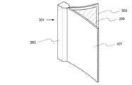
図15は、可撓性を有する液晶表示装置を2枚有する電子書籍301の斜視図である。電子書籍301は、綴じ部303に挟持された可撓性を有する液晶表示装置305、307を有する。また、液晶表示装置305は表示部309を有する。なお、図示しないが、液晶表示装置307の裏面、即ち表示部309と向かい合う面において、表示部を有する。FIG. 15 is a perspective view of an
可撓性を有する液晶表示装置305、307は、実施の形態4に示す可撓性を有する液晶表示装置を用いることができる。または、第1の基板及び第2の基板に、プリプレグを用いることで、可撓性を有する液晶表示装置の機械強度を高めることができる。As the flexible liquid
綴じ部303は中空を有する柱状または円柱状の筐体で形成されている。綴じ部303の中空には、液晶表示装置にFPC等のコネクターで接続された配線基板が内蔵される。また、配線基板上には、液晶表示装置305、307の表示を制御する半導体装置が実装される。また、配線基板に蓄電装置が電気的に接続される。また、綴じ部303に操作キーが設けられる。The binding
本実施の形態により、可撓性を有する液晶表示装置が湾曲しても、各画素におけるセルギャップが保持されるため、液晶表示装置の表示の乱れを低減することができる。このため、電子書籍の画質を向上させることができる。According to this embodiment mode, even when a flexible liquid crystal display device is curved, a cell gap in each pixel is maintained, so that display disorder of the liquid crystal display device can be reduced. For this reason, the image quality of an electronic book can be improved.
Claims (16)
Translated fromJapanese前記第1の基板に対向する第2の基板と、
前記第1の基板及び前記第2の基板の間において、規則的に配置され、且つ平面形状が対称性を有するスペーサと、
前記第1の基板及び前記第2の基板の間において形成される画素と、
を有し、
前記スペーサは、1つの前記画素において、1つ以上設けられることを特徴とする液晶表示装置。A first substrate;
A second substrate facing the first substrate;
A spacer regularly arranged between the first substrate and the second substrate and having a symmetrical planar shape;
A pixel formed between the first substrate and the second substrate;
Have
One or more of the spacers are provided in one of the pixels.
前記第1の基板に対向する第2の基板と、
前記第1の基板及び前記第2の基板の間において、規則的に配置され、且つ平面形状が対称性を有するスペーサと、
前記第1の基板及び前記第2の基板の間において形成される画素と、
を有し、
前記画素は、走査線、信号線、スイッチング素子、及び画素電極を有し、
前記スペーサの一は、少なくとも前記走査線と重畳して設けられ、
前記スペーサの二は、少なくとも前記信号線と重畳して設けられることを特徴とする液晶表示装置。A first substrate;
A second substrate facing the first substrate;
A spacer regularly arranged between the first substrate and the second substrate and having a symmetrical planar shape;
A pixel formed between the first substrate and the second substrate;
Have
The pixel includes a scanning line, a signal line, a switching element, and a pixel electrode,
One of the spacers is provided so as to overlap with at least the scanning line,
2. The liquid crystal display device according to claim 1, wherein at least two of the spacers are provided so as to overlap with the signal line.
前記第1の基板に対向する第2の基板と、
前記第1の基板及び前記第2の基板の間において、規則的に配置され、且つ平面形状が対称性を有するスペーサと、
前記第1の基板及び前記第2の基板の間において形成される画素と、
を有し、
前記画素は、走査線、信号線、スイッチング素子、及び画素電極を有し、
前記スペーサは、少なくとも前記走査線及び前記信号線の交差部に重畳して設けられることを特徴とする液晶表示装置。A first substrate;
A second substrate facing the first substrate;
A spacer regularly arranged between the first substrate and the second substrate and having a symmetrical planar shape;
A pixel formed between the first substrate and the second substrate;
Have
The pixel includes a scanning line, a signal line, a switching element, and a pixel electrode,
The liquid crystal display device, wherein the spacer is provided so as to overlap at least an intersection of the scanning line and the signal line.
Priority Applications (1)
| Application Number | Priority Date | Filing Date | Title |
|---|---|---|---|
| JP2011027107AJP2011186453A (en) | 2010-02-12 | 2011-02-10 | Liquid crystal display device |
Applications Claiming Priority (3)
| Application Number | Priority Date | Filing Date | Title |
|---|---|---|---|
| JP2010029292 | 2010-02-12 | ||
| JP2010029292 | 2010-02-12 | ||
| JP2011027107AJP2011186453A (en) | 2010-02-12 | 2011-02-10 | Liquid crystal display device |
Related Child Applications (1)
| Application Number | Title | Priority Date | Filing Date |
|---|---|---|---|
| JP2015094501ADivisionJP6117849B2 (en) | 2010-02-12 | 2015-05-05 | Liquid crystal display |
Publications (2)
| Publication Number | Publication Date |
|---|---|
| JP2011186453Atrue JP2011186453A (en) | 2011-09-22 |
| JP2011186453A5 JP2011186453A5 (en) | 2014-02-27 |
Family
ID=44792714
Family Applications (2)
| Application Number | Title | Priority Date | Filing Date |
|---|---|---|---|
| JP2011027107AWithdrawnJP2011186453A (en) | 2010-02-12 | 2011-02-10 | Liquid crystal display device |
| JP2015094501AExpired - Fee RelatedJP6117849B2 (en) | 2010-02-12 | 2015-05-05 | Liquid crystal display |
Family Applications After (1)
| Application Number | Title | Priority Date | Filing Date |
|---|---|---|---|
| JP2015094501AExpired - Fee RelatedJP6117849B2 (en) | 2010-02-12 | 2015-05-05 | Liquid crystal display |
Country Status (1)
| Country | Link |
|---|---|
| JP (2) | JP2011186453A (en) |
Cited By (5)
| Publication number | Priority date | Publication date | Assignee | Title |
|---|---|---|---|---|
| JP2013250458A (en)* | 2012-06-01 | 2013-12-12 | Semiconductor Energy Lab Co Ltd | Liquid crystal display device |
| JP2018132770A (en)* | 2012-10-12 | 2018-08-23 | 株式会社半導体エネルギー研究所 | Liquid crystal display device |
| JP2020181003A (en)* | 2019-04-23 | 2020-11-05 | シャープ株式会社 | Liquid crystal display device |
| US11809047B2 (en) | 2015-11-13 | 2023-11-07 | Dai Nippon Printing Co., Ltd. | Light transmission control film and laminated glass |
| JP7629496B2 (en) | 2015-08-28 | 2025-02-13 | 株式会社半導体エネルギー研究所 | Liquid crystal display device |
Families Citing this family (4)
| Publication number | Priority date | Publication date | Assignee | Title |
|---|---|---|---|---|
| KR101959488B1 (en)* | 2015-09-08 | 2019-03-18 | 주식회사 엘지화학 | Method of manufacturing an optical device |
| CN106597759B (en)* | 2017-02-24 | 2019-06-28 | 京东方科技集团股份有限公司 | Spacer material, display base plate and preparation method thereof, display panel |
| CN109932843B (en)* | 2017-12-15 | 2023-09-29 | 京东方科技集团股份有限公司 | Display panel and display device |
| CN115202106A (en)* | 2022-07-18 | 2022-10-18 | 华映科技(集团)股份有限公司 | Color film substrate and liquid crystal display panel |
Citations (8)
| Publication number | Priority date | Publication date | Assignee | Title |
|---|---|---|---|---|
| JPH04127128A (en)* | 1990-09-18 | 1992-04-28 | Sharp Corp | Active matrix display device |
| JPH04301621A (en)* | 1991-03-29 | 1992-10-26 | Casio Comput Co Ltd | Liquid crystal display element |
| JPH05158053A (en)* | 1991-12-05 | 1993-06-25 | Sharp Corp | Liquid crystal display manufacturing method |
| JPH1195194A (en)* | 1997-09-24 | 1999-04-09 | Toshiba Electronic Engineering Corp | Liquid crystal display device and method of manufacturing the same |
| JP2004069957A (en)* | 2002-08-06 | 2004-03-04 | Fujitsu Ltd | Liquid crystal display device |
| JP2004295109A (en)* | 2003-03-07 | 2004-10-21 | Semiconductor Energy Lab Co Ltd | Liquid crystal display device and manufacturing method therefor |
| JP2007232839A (en)* | 2006-02-28 | 2007-09-13 | Epson Imaging Devices Corp | Liquid crystal device |
| JP2009237010A (en)* | 2008-03-26 | 2009-10-15 | Epson Imaging Devices Corp | Liquid crystal panel |
Family Cites Families (6)
| Publication number | Priority date | Publication date | Assignee | Title |
|---|---|---|---|---|
| JP2006072388A (en)* | 1995-08-18 | 2006-03-16 | Toshiba Electronic Engineering Corp | Liquid crystal display element |
| JP3255107B2 (en)* | 1998-02-27 | 2002-02-12 | 東レ株式会社 | Color filter and liquid crystal display device using the same |
| JP2001242467A (en)* | 2000-02-29 | 2001-09-07 | Sanyo Electric Co Ltd | Liquid crystal display device and method of manufacturing |
| JP2002350863A (en)* | 2001-05-24 | 2002-12-04 | Seiko Epson Corp | Electro-optical device, method of manufacturing the same, and electronic apparatus |
| JP2003140159A (en)* | 2001-11-02 | 2003-05-14 | Sony Corp | Liquid crystal display element and its manufacturing method |
| JP5046005B2 (en)* | 2007-03-29 | 2012-10-10 | 大日本印刷株式会社 | Method for manufacturing element for liquid crystal display device |
- 2011
- 2011-02-10JPJP2011027107Apatent/JP2011186453A/ennot_activeWithdrawn
- 2015
- 2015-05-05JPJP2015094501Apatent/JP6117849B2/ennot_activeExpired - Fee Related
Patent Citations (8)
| Publication number | Priority date | Publication date | Assignee | Title |
|---|---|---|---|---|
| JPH04127128A (en)* | 1990-09-18 | 1992-04-28 | Sharp Corp | Active matrix display device |
| JPH04301621A (en)* | 1991-03-29 | 1992-10-26 | Casio Comput Co Ltd | Liquid crystal display element |
| JPH05158053A (en)* | 1991-12-05 | 1993-06-25 | Sharp Corp | Liquid crystal display manufacturing method |
| JPH1195194A (en)* | 1997-09-24 | 1999-04-09 | Toshiba Electronic Engineering Corp | Liquid crystal display device and method of manufacturing the same |
| JP2004069957A (en)* | 2002-08-06 | 2004-03-04 | Fujitsu Ltd | Liquid crystal display device |
| JP2004295109A (en)* | 2003-03-07 | 2004-10-21 | Semiconductor Energy Lab Co Ltd | Liquid crystal display device and manufacturing method therefor |
| JP2007232839A (en)* | 2006-02-28 | 2007-09-13 | Epson Imaging Devices Corp | Liquid crystal device |
| JP2009237010A (en)* | 2008-03-26 | 2009-10-15 | Epson Imaging Devices Corp | Liquid crystal panel |
Cited By (8)
| Publication number | Priority date | Publication date | Assignee | Title |
|---|---|---|---|---|
| JP2013250458A (en)* | 2012-06-01 | 2013-12-12 | Semiconductor Energy Lab Co Ltd | Liquid crystal display device |
| JP2018132770A (en)* | 2012-10-12 | 2018-08-23 | 株式会社半導体エネルギー研究所 | Liquid crystal display device |
| US10401662B2 (en) | 2012-10-12 | 2019-09-03 | Semiconductor Energy Laboratory Co., Ltd. | Liquid crystal display device and touch panel |
| JP2021103313A (en)* | 2012-10-12 | 2021-07-15 | 株式会社半導体エネルギー研究所 | Display device |
| JP7629496B2 (en) | 2015-08-28 | 2025-02-13 | 株式会社半導体エネルギー研究所 | Liquid crystal display device |
| US11809047B2 (en) | 2015-11-13 | 2023-11-07 | Dai Nippon Printing Co., Ltd. | Light transmission control film and laminated glass |
| JP2020181003A (en)* | 2019-04-23 | 2020-11-05 | シャープ株式会社 | Liquid crystal display device |
| JP7204573B2 (en) | 2019-04-23 | 2023-01-16 | シャープ株式会社 | liquid crystal display |
Also Published As
| Publication number | Publication date |
|---|---|
| JP6117849B2 (en) | 2017-04-19 |
| JP2015135530A (en) | 2015-07-27 |
Similar Documents
| Publication | Publication Date | Title |
|---|---|---|
| JP6117849B2 (en) | Liquid crystal display | |
| KR102547266B1 (en) | Liquid crystal display device | |
| US9570472B2 (en) | Array substrate and manufacturing method thereof, and liquid crystal display | |
| US9323116B2 (en) | Liquid crystal display device and fabrication method thereof | |
| US9678400B2 (en) | Array substrate for liquid crystal display and manufacturing method thereof | |
| US10050061B2 (en) | Array substrate and manufacturing method thereof, display device | |
| US9360726B2 (en) | Liquid crystal display | |
| KR20080071001A (en) | Liquid crystal display panel and manufacturing method thereof | |
| US20060187368A1 (en) | Array substrate, method of manufacturing the same, display panel having the same, and liquid crystal display apparatus having the same | |
| JP2015525000A (en) | Thin film transistor, array substrate, manufacturing method thereof, display | |
| US20160274428A1 (en) | Display device and method of manufacturing the same | |
| WO2014034512A1 (en) | Thin film transistor substrate and display device | |
| KR20060115464A (en) | LCD and its manufacturing method | |
| US20240142829A1 (en) | Array substrate and manufacturing method therefor, display assembly, and display device | |
| KR101362960B1 (en) | Liquid crystal display device and fabricating method thereof | |
| EP3686664A1 (en) | Display panel and manufacturing method thereof and display device | |
| KR101631620B1 (en) | Fringe field switching liquid crystal display device and method of fabricating the same | |
| KR20170097273A (en) | Display device and manufacturing method thereof | |
| KR20090043838A (en) | Liquid crystal display panel and its manufacturing method | |
| US10996520B2 (en) | Display device comprising an insulating layer disposed betweeen a first pixel electrode in a first pixel area and a second pixel electrode in a second pixel area | |
| US9864248B2 (en) | Semiconductor device and display device | |
| CN111856825A (en) | Array substrate and preparation method thereof, display panel and display device | |
| KR101627518B1 (en) | In Plane Switching mode Liquid Crystal Display Device and Method for Manufacturing Thereof | |
| WO2013008402A1 (en) | Thin-film transistor substrate and display device comprising same | |
| KR102145279B1 (en) | Thin Film Transistor Array Substrate and Method of manufacturing the same |
Legal Events
| Date | Code | Title | Description |
|---|---|---|---|
| A521 | Written amendment | Free format text:JAPANESE INTERMEDIATE CODE: A523 Effective date:20140108 | |
| A621 | Written request for application examination | Free format text:JAPANESE INTERMEDIATE CODE: A621 Effective date:20140108 | |
| A977 | Report on retrieval | Free format text:JAPANESE INTERMEDIATE CODE: A971007 Effective date:20140925 | |
| A131 | Notification of reasons for refusal | Free format text:JAPANESE INTERMEDIATE CODE: A131 Effective date:20140930 | |
| A131 | Notification of reasons for refusal | Free format text:JAPANESE INTERMEDIATE CODE: A131 Effective date:20150303 | |
| A521 | Written amendment | Free format text:JAPANESE INTERMEDIATE CODE: A523 Effective date:20150310 | |
| A02 | Decision of refusal | Free format text:JAPANESE INTERMEDIATE CODE: A02 Effective date:20150407 | |
| A761 | Written withdrawal of application | Free format text:JAPANESE INTERMEDIATE CODE: A761 Effective date:20150506 |