JP2011171422A - Field-effect transistor - Google Patents
Field-effect transistorDownload PDFInfo
- Publication number
- JP2011171422A JP2011171422AJP2010032281AJP2010032281AJP2011171422AJP 2011171422 AJP2011171422 AJP 2011171422AJP 2010032281 AJP2010032281 AJP 2010032281AJP 2010032281 AJP2010032281 AJP 2010032281AJP 2011171422 AJP2011171422 AJP 2011171422A
- Authority
- JP
- Japan
- Prior art keywords
- layer semiconductor
- barrier layer
- semiconductor
- field effect
- effect transistor
- Prior art date
- Legal status (The legal status is an assumption and is not a legal conclusion. Google has not performed a legal analysis and makes no representation as to the accuracy of the status listed.)
- Granted
Links
Images


Landscapes
- Junction Field-Effect Transistors (AREA)
- Thin Film Transistor (AREA)
- Insulated Gate Type Field-Effect Transistor (AREA)
Abstract
Translated fromJapaneseDescription
Translated fromJapanese本発明は、電界効果型トランジスタに係り、特に、分極電荷埋め込みチャネル構造の電界効果型トランジスタに関する。 The present invention relates to a field effect transistor, and more particularly to a field effect transistor having a polarization charge buried channel structure.
窒化物半導体を用いた電界効果トランジスタ(Field Effect Transistor(FET)、GaN系FET、ヘテロ構造電界効果トランジスタ(Heterostructure Field Effect Transistor: HFET)を含む)は、次世代の高温、高出力、高耐圧の高周波トランジスタとして非常に有望であり、実用化に向けて現在盛んに研究が行われている。 Nitride semiconductor field effect transistors (including field effect transistors (FETs), GaN-based FETs, and heterostructure field effect transistors (HFETs)) are the next generation of high temperature, high power, high withstand voltage. It is very promising as a high-frequency transistor, and is actively researched for practical use.
上記したFETのうちGaN系のHFETは、通常、極性面上(すなわちc軸方向)に形成されるため、ヘテロ界面に大きな分極電荷が存在する。このため、キャリア供給のためのドーピングを施さなくても、伝導に寄与するキャリア(チャネル電子(2次元電子))がチャネルに誘起される。 Of the above-described FETs, GaN-based HFETs are usually formed on the polar plane (that is, in the c-axis direction), and therefore there is a large polarization charge at the heterointerface. For this reason, carriers (channel electrons (two-dimensional electrons)) that contribute to conduction are induced in the channel without doping for carrier supply.
このため、GaN系のHFETは、大電流が得られやすいという有利な面があるため、一般的に、いわゆるデプレション型のデバイス動作に向いている。また、これと相反するエンハンスメント型のデバイス動作も可能ではあることが報告されているものの、エンハンスメント型のデバイス動作には不向きであり、高い正のしきい値電圧を得ることが困難であることが、非特許文献1に記載されている。 For this reason, a GaN-based HFET has an advantageous aspect that a large current is easily obtained, and thus is generally suitable for a so-called depletion type device operation. Although it has been reported that enhancement-type device operation contrary to this is possible, it is not suitable for enhancement-type device operation, and it may be difficult to obtain a high positive threshold voltage. Non-Patent Document 1.
なお、デプレション型のデバイスとは、しきい値電圧が負の値であって、ノーマリーオン型とも呼ばれるデバイスである。デプレション型のデバイス動作とは、ゲートに電圧を印加しない状態、すなわちゲート電圧ゼロの場合であってもドレイン電圧の印加によってドレイン電流が流れ、ゲートに負の電圧を印加することによってドレイン電流がゼロになる(すなわちピンチオフする)デバイス動作をいう。 Note that a depletion type device is a device whose threshold voltage is a negative value and is also referred to as a normally-on type. The depletion type device operation is a state in which no voltage is applied to the gate, that is, even when the gate voltage is zero, the drain current flows by applying the drain voltage, and the drain current is generated by applying a negative voltage to the gate. Device operation that goes to zero (ie, pinches off).
一方、エンハンスメント型のデバイスとは、しきい値電圧が正の値であって、ノーマリーオフ型とも呼ばれるデバイスである。エンハンスメント型のデバイス動作とは、ゲートに電圧を印加しない状態、すなわちゲート電圧ゼロの場合にはドレイン電圧の印加によってもドレイン電流が流れず、ゲートに正の電圧を印加することによってドレイン電流が流れるデバイス動作をいう。 On the other hand, an enhancement type device is a device whose threshold voltage is a positive value and is also called a normally-off type device. The enhancement type device operation is a state where no voltage is applied to the gate, that is, when the gate voltage is zero, the drain current does not flow even when the drain voltage is applied, and the drain current flows when the positive voltage is applied to the gate. Refers to device operation.
以下、このようなGaN系のエンハンスメント型の電界効果トランジスタ(以下、簡単のため、GaN系エンハンスメント型FETと記す)のデバイス動作について、より詳細に説明する。 The device operation of such a GaN enhancement type field effect transistor (hereinafter referred to as a GaN enhancement type FET for simplicity) will be described in more detail below.
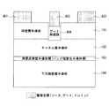
図6は、従来のGaN系エンハンスメント型FETを説明するための図である。図示したGaN系エンハンスメント型FETでは、極性面である+c面((0001)面)上に、障壁層半導体605、チャネル層半導体606による障壁層半導体/チャネル層半導体へテロ構造が形成されている。 FIG. 6 is a diagram for explaining a conventional GaN-based enhancement type FET. In the illustrated GaN-based enhancement type FET, a barrier layer semiconductor / channel layer semiconductor heterostructure including a
障壁層半導体/チャネル層半導体へテロ構造上には、ソース電極601、ゲート電極602、ドレイン電極603が形成されている。GaN系エンハンスメント型FETにあっては、ゲート電極602の下方に存在する障壁層半導体605の層の厚さ(以降、「層厚」と記す)が一般に小さいことが特徴となっている。 A
図6に示した構造では、高いゲート耐圧を得るために、ゲート電極602と障壁層半導体605の間に絶縁膜が挿入された、いわゆる絶縁ゲート(あるいはMIS(MIS:Metal-Insulator-Semiconductor))構造が用いられている。また、図6に示した構造では、低いソース抵抗を得るために、ソース電極601、ゲート電極602間、及びゲート電極602、ドレイン電極603間の障壁層半導体605の層厚が、ゲート電極602の下方に存在する障壁層半導体605の層厚に比べて大きい、いわゆるリセスゲート構造が用いられている。 In the structure shown in FIG. 6, a so-called insulated gate (or MIS (Metal-Insulator-Semiconductor)) in which an insulating film is inserted between the
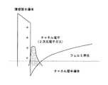
図7は、図6に示したGaN系エンハンスメント型FETの、ゲート電極602の下方に存在する障壁層半導体605(以下、チャネルと記す)の層構造のポテンシャル(以下、チャネル・ポテンシャルと記す)の形状を模式的に示したものである。 7 shows the potential of the layer structure (hereinafter referred to as channel potential) of the barrier layer semiconductor 605 (hereinafter referred to as channel) existing below the
図6に示した障壁層半導体/チャネル層半導体へテロ界面には正の分極電荷が存在するため、半導体基板にキャリア供給のためのドーピングが施されていなくても、2次元電子がチャネルのヘテロ界面近傍に誘起される。図7には、誘起された2次元電子がチャネル電子となっている様子が示されている。 Since there is a positive polarization charge at the barrier layer semiconductor / channel layer semiconductor hetero interface shown in FIG. 6, even if the semiconductor substrate is not doped for carrier supply, the two-dimensional electrons are heterogeneous in the channel. Induced near the interface. FIG. 7 shows that the induced two-dimensional electrons are channel electrons.
GaN系エンハンスメント型FETのチャネル構造は、その特徴として、障壁層半導体605の層厚が薄く設計されている。このため、障壁層半導体の層厚がより大きいデプレション型FETに比べて2次元電子濃度が低くなる。その結果、GaN系エンハンスメント型FETでは、しきい値電圧が正の方向に移動することにより、エンハンスメント型のデバイス動作が擬似的に実現される。 As a feature of the channel structure of the GaN-based enhancement type FET, the
しかしながら、電力応用においては、デプレション型のデバイス動作と同時に、エンハンスメント型のデバイス動作の実現が必須である。そこで、通常の極性面上(すなわちc軸方向)に形成するエンハンスメント型のデバイスにおいて高い正のしきい値が実現可能なFETを開発することが強く望まれていた。 However, in power applications, it is essential to realize enhancement type device operation simultaneously with depletion type device operation. Therefore, it has been strongly desired to develop an FET capable of realizing a high positive threshold in an enhancement type device formed on a normal polar plane (that is, in the c-axis direction).
本発明は、上記した点に鑑みてなされたものであって、チャネル構造を変更することなく、チャネルのしきい値電圧がより高いエンハンスメント型の電界効果型トランジスタを提供することを目的とする。 The present invention has been made in view of the above points, and an object of the present invention is to provide an enhancement type field effect transistor having a higher channel threshold voltage without changing the channel structure.
以上述べた課題を解決するため、本発明の請求項1に記載の電界効果トランジスタは、複数層の窒化物半導体を有する電界効果トランジスタにおいて、前記複数層の窒化物半導体のうち、電界効果トランジスタにおける電気伝導に寄与するキャリアが走行するチャネル層半導体(例えば図4に示したチャネル層半導体102)と、前記チャネル層半導体よりも下層にあって、当該チャネル層半導体よりもバンドギャップの大きい窒化物半導体からなる下方障壁層半導体(例えば図4に示した下方障壁層半導体104)と、前記チャネル層半導体と前記下方障壁層半導体との間にあって、バンドギャップが前記下方障壁層半導体のバンドギャップより大きい薄高障壁層半導体(例えば図4に示した薄高障壁層半導体103)と、を含む層構造を有することを特徴とする。 In order to solve the above-described problems, a field effect transistor according to claim 1 of the present invention is a field effect transistor having a plurality of nitride semiconductors, and in the field effect transistor of the plurality of nitride semiconductors. A channel layer semiconductor (for example, the
このような発明によれば、見かけ上、従来構造のチャネル層半導体中に負の分極電荷を埋め込んだものと同等の状況が実現でき、その結果、チャネル層半導体のポテンシャルが高くなり、高い正のしきい値が実現される。 According to such an invention, apparently, a situation equivalent to that in which a negative polarization charge is embedded in a channel layer semiconductor having a conventional structure can be realized, and as a result, the potential of the channel layer semiconductor is increased, and a high positive A threshold is realized.
また、請求項2に記載の電界効果型トランジスタは、請求項1に記載の発明において、前記薄高障壁層半導体のバンドギャップ及び厚さが、前記チャネル層半導体のバンド端と前記下方障壁層半導体のバンド端の位置が略一致することを特徴とする。 According to a second aspect of the present invention, in the field effect transistor according to the first aspect of the present invention, the band gap and thickness of the thin high barrier layer semiconductor are such that the band edge of the channel layer semiconductor and the lower barrier layer semiconductor are The positions of the band ends are substantially the same.
このような発明によれば、チャネル層半導体のポテンシャルを高くし、しかも下方障壁層半導体と薄高障壁層半導体とのへテロ界面近傍に副次的チャネルが発生することを防ぐことができる。 According to such an invention, it is possible to increase the potential of the channel layer semiconductor and to prevent the generation of a secondary channel in the vicinity of the heterointerface between the lower barrier layer semiconductor and the thin high barrier layer semiconductor.
また、請求項3に記載の電界効果型トランジスタは、請求項2において、前記チャネル層半導体と前記薄層高障壁半導体との界面に発生する分極電荷と、前記薄層高障壁半導体と前記下方障壁層半導体との界面に発生する分極電荷とによって、前記薄高障壁層半導体内部に形成される電界と、前記薄高障壁層半導体の厚さとの積によって与えられる前記薄高障壁層半導体の両端でのバンド端位置の差が、前記チャネル層半導体と前記下方障壁層半導体とのバンド端位置の差に略等しいことを特徴とする。 The field effect transistor according to claim 3 is the field effect transistor according to claim 2, wherein the polarization charge generated at the interface between the channel layer semiconductor and the thin high barrier semiconductor, the thin high barrier semiconductor, and the lower barrier are provided. At both ends of the thin high barrier layer semiconductor given by the product of the electric field formed inside the thin high barrier layer semiconductor and the thickness of the thin high barrier layer semiconductor due to polarization charges generated at the interface with the layer semiconductor. The difference between the band edge positions is substantially equal to the difference between the band edge positions of the channel layer semiconductor and the lower barrier layer semiconductor.
このような発明によれば、薄高障壁層半導体内部に形成される電界と薄高障壁層半導体の厚さとの積により、チャネル層半導体のポテンシャルを高くし、しかも下方障壁層半導体と薄高障壁層半導体とのへテロ界面近傍に副次的チャネルが発生することを防ぐことができる。 According to such an invention, the potential of the channel layer semiconductor is increased by the product of the electric field formed inside the thin high barrier layer semiconductor and the thickness of the thin high barrier layer semiconductor, and the lower barrier layer semiconductor and the thin high barrier are further increased. A secondary channel can be prevented from being generated in the vicinity of the hetero interface with the layer semiconductor.
請求項4に記載の電界効果型トランジスタは、請求項1から3のいずれか1項において、GaN系電界効果型トランジスタ、またはヘテロ構造電界効果トランジスタ(Heterostructure Field Effect Transistor:HFET)であることを特徴とする。 The field effect transistor according to claim 4 is the GaN-based field effect transistor or heterostructure field effect transistor (HFET) according to any one of claims 1 to 3. And
このような発明によれば、GaN系電界効果型トランジスタ、ヘテロ構造電界効果トランジスタに本発明の電界効果型トランジスタを適用することができる。 According to such an invention, the field effect transistor of the present invention can be applied to a GaN-based field effect transistor and a heterostructure field effect transistor.
請求項5に記載の電界効果型トランジスタは、請求項1から4のいずれか1項において、前記薄高障壁層半導体の厚さが、0.5nm以上、5nm以下であることを特徴とする。 A field effect transistor according to a fifth aspect is characterized in that, in any one of the first to fourth aspects, the thickness of the thin high barrier layer semiconductor is 0.5 nm or more and 5 nm or less.
このような発明によれば、チャネル層半導体のポテンシャルを高くし、しかも下方障壁層半導体と薄高障壁層半導体とのへテロ界面近傍に副次的チャネルが発生することを防ぐ薄高障壁層半導体の厚さを最適化することができる。 According to such an invention, the thin high barrier layer semiconductor that increases the potential of the channel layer semiconductor and prevents the generation of a secondary channel in the vicinity of the heterointerface between the lower barrier layer semiconductor and the thin high barrier layer semiconductor. The thickness of the can be optimized.
本発明は、チャネル構造を変更することなく、チャネルのしきい値電圧がより高いエンハンスメント型の電界効果型トランジスタを提供することができる。 The present invention can provide an enhancement type field effect transistor having a higher channel threshold voltage without changing the channel structure.
以下、本発明の電界効果型トランジスタの実施形態1、実施形態2を説明する。なお、実施形態1、実施形態2でいう電界効果型トランジスタ(Field Effect Transistor(FET)は、GaN系FET、ヘテロ構造電界効果トランジスタ(Heterostructure Field Effect Transistor: HFET)を含むものとする。 Embodiments 1 and 2 of the field effect transistor of the present invention will be described below. The field effect transistor (FET) referred to in the first and second embodiments includes a GaN-based FET and a heterostructure field effect transistor (HFET).
(理論)
本明細書では、実施形態1、実施形態2の具体的な構成に先立って、実施形態1、実施形態2の電界効果型トランジスタが作用、効果を奏する理論について説明する。(theory)
In this specification, prior to the specific configurations of the first and second embodiments, the theory that the field-effect transistors of the first and second embodiments function and exert an effect will be described.
図1は、本発明の実施形態1、実施形態2の電界効果型トランジスタのチャネル構造を説明するための模式図である。実施形態1、実施形態2の電界効果型トランジスタのチャネル構造は、分極電荷埋め込みチャネル構造である。図示したチャネルは、ゲート電極下に存在する障壁層半導体101、障壁層半導体101と共に障壁層半導体/チャネル層半導体へテロ構造を形成するチャネル層半導体102を有している。 FIG. 1 is a schematic diagram for explaining a channel structure of a field effect transistor according to Embodiments 1 and 2 of the present invention. The channel structure of the field effect transistor of Embodiments 1 and 2 is a polarization charge buried channel structure. The illustrated channel includes a
さらに、実施形態1、実施形態2の電界効果型トランジスタは、チャネル層半導体102よりも下層に、チャネル層半導体102よりもバンドギャップの大きい窒化物半導体からなる下方障壁層半導体104を有している。チャネル層半導体102と下方障壁層半導体104との間には、バンドギャップが下方障壁層半導体104のバンドギャップより大きい、薄高障壁層半導体(図中にバンド端整合半導体層とも記す)103が挿入されている。薄高障壁層半導体103は、0.5nm以上、5nm以下の厚さを有するものとする。 Furthermore, the field effect transistors of Embodiments 1 and 2 have a lower
このような実施形態1、実施形態2の電界効果型トランジスタは、チャネル層半導体/薄高障壁層半導体/下方障壁層半導体の層構造を有するものであればよく、チャネル層半導体102上の障壁層半導体101の有無に限定されるものではない。なお、障壁層半導体101がある場合、実施形態1、実施形態2の電界効果型トランジスタはHFETとなる。障壁層半導体101がない場合、実施形態1、実施形態2の電界効果型トランジスタはFETとなる。 The field effect transistors according to the first and second embodiments are only required to have a layer structure of channel layer semiconductor / thin high barrier layer semiconductor / lower barrier layer semiconductor, and the barrier layer on the
図2は、図1に示した電界効果型トランジスタのチャネル・ポテンシャルの形状を模式的に示した図である。図1に示したチャネル層半導体/薄高障壁層半導体の界面に発生する分極電荷と、薄高障壁層半導体/下方障壁層半導体の界面に発生する分極電荷は、薄高障壁層半導体103の内部に形成される電界と、薄高障壁層半導体103の厚さ(以降、層厚と記す)との積によって与えられる。 FIG. 2 is a diagram schematically showing the shape of the channel potential of the field effect transistor shown in FIG. The polarization charge generated at the interface between the channel layer semiconductor / thin high barrier layer semiconductor and the polarization charge generated at the interface between the thin high barrier layer semiconductor / lower barrier layer semiconductor shown in FIG. , And the thickness of the thin high barrier layer semiconductor 103 (hereinafter referred to as layer thickness).
薄高障壁層半導体103の両端において、バンド端(伝導帯端)位置(バンド端のエネルギー的なレベル)の差は、チャネル層半導体102と下方障壁層半導体104とのバンド端位置の差に等しくなるように設計されている。この結果、薄高障壁層半導体103の両端において、チャネル層半導体102のバンド端と下方障壁層半導体104のバンド端の位置が一致する。図2には、この状態が模式的に示されている。 At both ends of the thin high
薄高障壁層半導体103の両端に生じる正味の分極電荷は負となり、この負電荷によって、チャネル層半導体102のポテンシャルの位置がより高くなる。この結果、2次元電子がより強固に空乏化し、FET動作において高い正のしきい値が実現可能となる。具体的な設計条件は後述するものとする。 The net polarization charge generated at both ends of the thin high
次に、図2に示した、薄高障壁層半導体103の両端でチャネル層半導体のバンド端と下方障壁層半導体のバンド端の位置が一致することの意味について説明する。 Next, the meaning of the positions of the band edge of the channel layer semiconductor and the band edge of the lower barrier layer semiconductor at both ends of the thin high
図3は、薄高障壁層半導体103を設けることなく、チャネル層半導体102の直下に下方障壁層半導体104を設けた場合のチャネル・ポテンシャルの形状を模式的に示した図である。チャネル層半導体102の直上に障壁半導体101が存在するHFETの場合、いわゆるダブル・ヘテロ構造チャネルのチャネル・ポテンシャルの形状に等しい形状のチャネル・ポテンシャルが発生する。 FIG. 3 is a diagram schematically showing the shape of the channel potential when the lower
図3において、チャネル層半導体/下方障壁層半導体界面に生じる負の分極電荷は、図2に示した薄高障壁層半導体の正味の負電荷と等量である。そのため、図3においても、チャネル層半導体102のポテンシャルを図2に示した場合と同様に高くすることになる。しかし、図3に示した例では、ヘテロ界面におけるバンド端不連続によって、チャネル層半導体102のポテンシャルは図2におけるチャネル層半導体102のポテンシャルに比べて低くなっている。したがって、図3に示した例は、FET動作におけるしきい値電圧が、図2に示した場合に比べて低くなる。 In FIG. 3, the negative polarization charge generated at the channel layer semiconductor / lower barrier layer semiconductor interface is equivalent to the net negative charge of the thin high barrier layer semiconductor shown in FIG. Therefore, also in FIG. 3, the potential of the
また、図3に示した場合と反対に、図2に示した薄高障壁層半導体103が、チャネル層半導体102のポテンシャルをさらに高くするために、薄高障壁層半導体103の両端において、チャネル層半導体102のバンド端の位置が、下方障壁層半導体104のバンド端の位置よりも高くなるように設計することが考えられる。しかし、このような場合には、下方障壁層半導体104側の薄高障壁層半導体/下方障壁層半導体へテロ界面近傍に2次元電子が生じ、これが副次的チャネルとして作用するという不具合が生じる。 In contrast to the case shown in FIG. 3, the thin high
以上のことから、図2に示したように、薄高障壁層半導体103の両端において、チャネル層半導体102のバンド端の位置と下方障壁層半導体104のバンド端の位置が一致するように設計することにより、上記した副次的チャネルが生じる不具合を回避しながらチャネル層半導体102のポテンシャルを最大限に高めることが可能となる。すなわち、実施形態1、実施形態2の電界効果型トランジスタでは、チャネル層半導体中に負の分極電荷を埋め込んだ構造と見かけ上同等の状況を実現することが可能となる。その結果、チャネル層半導体のポテンシャルが高くなり、デバイス動作において高いしきい値電圧を実現することができる。 From the above, as shown in FIG. 2, it is designed so that the band edge position of the
(実施形態1)
次に、以上の理論に基づいて構成された、実施形態1の電界効果型トランジスタを説明する。(Embodiment 1)
Next, the field effect transistor according to Embodiment 1 configured based on the above theory will be described.
図4は、本発明の実施形態1の電界効果型トランジスタを説明するための図である。図4中、図1に示した構成と同様の構成については同様の符号を付し、その説明を一部略すものとする。 FIG. 4 is a diagram for explaining the field effect transistor according to the first embodiment of the present invention. In FIG. 4, the same components as those shown in FIG. 1 are denoted by the same reference numerals, and the description thereof is partially omitted.
実施形態1の電界効果型トランジスタは、下方障壁層半導体104、薄高障壁層半導体103、チャネル層半導体102、障壁層半導体101を順に積層して構成されている。障壁層半導体101上にはソース電極401、ゲート電極402、ドレイン電極403が形成されている。ソース電極401、ゲート電極402、ドレイン電極403はいずれも金属電極である。また、実施形態1の電界効果トランジスタは、リセスゲート構造を有していて、ゲート電極402下の障壁層半導体101に凹部101aが形成されている。凹部101a内にはゲート絶縁膜404が形成されている。 The field effect transistor according to the first embodiment is configured by sequentially laminating a lower
下方障壁層半導体104は、チャネル層半導体102よりもバンドギャップの大きい窒化物半導体からなる。薄高障壁層半導体103は、下方障壁層半導体104よりも大きいバンドギャップを有し、その層厚は0.5nm以上、5nm以下とする。 The lower
薄高障壁層半導体103のバンドギャップ及び層厚は、チャネル層半導体102のバンド端の位置と下方障壁層半導体104のバンド端の位置が一致するように設計されている。すなわち、チャネル層半導体/薄高障壁層半導体の界面に発生する分極電荷及び薄高障壁層半導体/下方障壁層半導体の界面に発生する分極電荷によって薄高障壁層半導体103内部に形成される電界と、薄高障壁層半導体103の層厚との積によって与えられる薄高障壁層半導体の両端でのバンド端位置の差が、チャネル層半導体102と下方障壁層半導体104とのバンド端位置の差に等しくなるように設計されている。 The band gap and the layer thickness of the thin and high
このことから、実施形態1では、薄高障壁層半導体103を図中にバンド端整合半導体層とも記す。 Therefore, in the first embodiment, the thin high
実施形態1の障壁層半導体101にはAlX1Ga1−X1N(0<X1≦1)、チャネル層半導体102にはGaN、下方障壁層半導体104にはAlX2Ga1−X2N(0<X2≦1)、薄高障壁層半導体103には層厚0.5nm以上、5nm以下のAlX3Ga1−X3N(0<X2<X3<1)が用いられている。The
障壁層半導体101の層厚は任意である。下方障壁層半導体104の層厚は任意であるが、バッファ層であるため、一般的に100nm以上であり、多くの場合、1〜3μm程度の厚膜である。薄高障壁層半導体103の層厚は、挿入層として有意であるために0.5nm以上の層厚が必要である。一方、薄高障壁層半導体103の層厚が5nmを超えると、下方障壁層半導体104における薄高障壁層半導体103との界面近傍に2次元電子が生じ得る。このため、薄高障壁層半導体103の層厚の上限は5nmとする。 The layer thickness of the
図4に示した電界効果型トランジスタにおいて、チャネル層半導体102及び下方障壁層半導体104のバンド端の位置の差(バンド端不連続)ΔECは、次式で与えられる。In the field effect transistor shown in FIG. 4, the difference in band edge position (band edge discontinuity) ΔEC between the
ΔEC=0.75×(6.2−3.4)×X2=2.1×X2 [eV] …式(1)
なお、上記した式において、GaNのバンドギャップは3.4[eV]、AlNのバンドギャップは6.2[eV]。バンド端不連続はバンドギャップ差の0.75倍とする。ΔEC = 0.75 × (6.2-3.4) × X2 = 2.1 × X2 [eV] Formula (1)
In the above formula, the band gap of GaN is 3.4 [eV], and the band gap of AlN is 6.2 [eV]. The band edge discontinuity is 0.75 times the band gap difference.
また、薄高障壁層半導体103の両端に生じる分極電荷によって薄高障壁層半導体103内部に電界が形成される。形成された電界により、薄高障壁層半導体103の両端に生じるポテンシャルの差ΔEbは式(2)で与えられる。式(2)は、系の分極効果の詳細が考慮された最終結果である。式中のdは、薄高障壁層半導体103の層厚を示す。In addition, an electric field is formed inside the thin high
ΔEb=1.02×(X3−X2)×d [eV] …式(2)
したがって、薄高障壁層半導体103のAlX3Ga1−X3N(0<X2<X3<1)のAl組成X3(0<X2<X3<1)と層厚dnm(0.5nm≦d≦5nm)との間に要求される条件は、次の式(3)で与えられる。なお、式(3)は、ΔEC=ΔEbの条件の下導き出されたものである。ΔEb = 1.02 × (X3−X2) × d [eV] (2)
Therefore, the Al composition X3 (0 <X2 <X3 <1) of AlX3 Ga1-X3 N (0 <X2 <X3 <1) and the layer thickness dnm (0.5 nm ≦ d ≦ 5 nm) of the thin high barrier layer semiconductor 103. ) Is given by the following equation (3). Equation (3) is derived under the condition of ΔEC = ΔEb .
2.1×X2[eV]=1.02×(X3−X2)×d[eV] …式(3)
式(3)により、実施形態1における薄高障壁層半導体103の設計条件は、以下の式(4)、(5)のように表される。2.1 * X2 [eV] = 1.02 * (X3-X2) * d [eV] Formula (3)
From the equation (3), the design condition of the thin high
0<X2<X3<1 …式(4)
0.5nm≦d≦5nm) …式(5)
ただし、式(3)の両辺の値の差異が、0.05[eV]以下である場合、実施形態1では物理的に等式が成り立つとみなすことができる。このため、このような場合にも実施形態1の設計条件を満たすものとする。0 <X2 <X3 <1 Formula (4)
0.5 nm ≦ d ≦ 5 nm) Formula (5)
However, when the difference between the values on both sides of Equation (3) is 0.05 [eV] or less, it can be considered that the equation is physically established in the first embodiment. For this reason, even in such a case, the design condition of the first embodiment is satisfied.
また、薄高障壁層半導体103は、その挿入位置に係らず電界効果型トランジスタに負電荷を与えることが可能である。このため、薄高障壁層半導体103の挿入位置は任意とする。 In addition, the thin high
実施形態1では、以上説明した設計条件に基づいて、図4に示した電界効果型トランジスタを以下のように構成した。すなわち、実施形態1の電界効果型トランジスタには、障壁層半導体101としてAl0.3Ga0.7Nが使用されている。Al0.3Ga0.7Nの層厚は、ゲート電極402下で2nm、ゲート電極402下以外では20nmである。チャネル層半導体102には層厚40nmのGaN、下方障壁層半導体104には層厚1.5μmのAl0.2Ga0.8Nが用いられている。薄高障壁層半導体103は、層厚2nmのAl0.3Ga0.7Nである。In the first embodiment, the field effect transistor shown in FIG. 4 is configured as follows based on the design conditions described above. That is, Al0.3 Ga0.7 N is used as the
このような障壁層半導体101、チャネル層半導体102、薄高障壁層半導体103、下方障壁層半導体104は、c面サファイア基板、SiC基板あるいはSi基板上に、有機金属気相成長法(MOVPE: Metal Organic Vapor Phase Epitaxy)等の結晶成長法によって成長される。このようなプロセスにより、20nmAl0.3Ga0.7N/40nmGaN/2nmAl0.3Ga0.7N/1.5μmAl0.2Ga0.8N構造が形成される。Such
20nmAl0.3Ga0.7N/40nmGaN/2nmAl0.3Ga0.7N/1.5μmAl0.2Ga0.8N構造を、ドライエッチング法等の周知のプロセス技術によってエッチングすることにより、図4に示したリセスゲート構造が形成される。形成されたリセスゲート構造の凹部101aには、ゲート絶縁膜404として30nmのAl2O3膜が形成される。実施形態1では、以上の工程により、+8Vの高いしきい値電圧を有するエンハンスメント型の電界効果型トランジスタが実現された。By etching a 20 nm Al0.3 Ga0.7 N / 40 nm GaN / 2 nm Al0.3 Ga0.7 N / 1.5 μm Al0.2 Ga0.8 N structure by a known process technique such as a dry etching method. Thus, the recessed gate structure shown in FIG. 4 is formed. A 30 nm Al2 O3 film is formed as the
また、実施形態1は、このような構成に限定されるものではない。すなわち、実施形態1は、薄高障壁層半導体103のバンドギャップ及び層厚が、チャネル層半導体102のバンド端の位置と下方障壁層半導体104のバンド端の位置が一致するように設計されていればよい。 Further, the first embodiment is not limited to such a configuration. That is, the first embodiment is designed such that the band gap and the layer thickness of the thin and high
したがって、実施形態1は、図4に示したように、障壁層半導体101としてAlX1Ga1−X1N(0<X1≦1)、チャネル層半導体102としてGaN、下方障壁層半導体104としてAlX2Ga1−X2N(0<X2≦1)、薄高障壁層半導体として層厚0.5nm以上、5nm以下のAlX3Ga1−X3N(0<X2<X3<1)を用いるものに限定されるものではなく、他の窒化物半導体を用いるものであってもよい。他の窒化物としては、例えば、AlGaN、nGaN、nN、InAlN、nAlGaN、lNを含むいかなる窒化物半導体であってもよい。Therefore, in the first embodiment, as shown in FIG. 4, AlX1 Ga1-X1 N (0 <X1 ≦ 1) as the
また、実施形態1は、ゲート電極402下以外の構造について図4に示した構造と異なるものであってもよい。例えば、ゲート電極402下以外の領域は、例えば、再成長GaNによって形成されているような場合であっても、ゲート電極402の下方の窒化物半導体チャネル構造が以上説明した特徴を有する限り本発明に含まれる。また、窒化物層半導体の一部あるいは全部に、窒化物層半導体のポテンシャルを高めるために、Mg等のドーパントがドーピングされている場合であっても、ゲート電極402下方の窒化物半導体チャネル構造が以上説明した特徴を有する限り本発明の効果を有する。したがって、このような構成も本発明に含まれることは言うまでもない。 Further, the first embodiment may be different from the structure shown in FIG. For example, even if the region other than under the
(実施形態2)
次に、本発明の実施形態2について説明する。(Embodiment 2)
Next, Embodiment 2 of the present invention will be described.
図5は、本発明の実施形態2の電界効果型トランジスタを説明するための図である。なお、図5において、図1に示した構成と同様の構成については同様の符号を付して示し、説明の一部を略す。 FIG. 5 is a diagram for explaining a field effect transistor according to the second embodiment of the present invention. In FIG. 5, the same components as those shown in FIG. 1 are denoted by the same reference numerals, and a part of the description is omitted.
実施形態2の電界効果型トランジスタは、ゲート電極402下の障壁層半導体101が全て除去されている点で実施形態1の電界効果型トランジスタと相違する。実施形態2の電界効果型トランジスタは、ゲート電極402下の障壁層半導体101が完全に除去されているため、一般的にはチャネル電子の移動度が低下するという不利な点を有する。しかし、チャネル層半導体102のポテンシャルがより高くなる結果、より高いしきい値が得られる効果を奏する。 The field effect transistor of the second embodiment is different from the field effect transistor of the first embodiment in that all of the
本発明の発明者らは、AlGaN障壁層が完全に除去された実施形態2の電界効果型トランジスタを製造した。この結果、実施形態1の電界効果型トランジスタよりも利得が20%低下するものの、+10Vという、実施形態1の電界効果型トランジスタより高いしきい値電圧を有する電界効果型トランジスタを得ることができた。 The inventors of the present invention manufactured the field effect transistor of Embodiment 2 in which the AlGaN barrier layer was completely removed. As a result, although the gain is 20% lower than that of the field effect transistor of the first embodiment, a field effect transistor having a threshold voltage of +10 V higher than that of the field effect transistor of the first embodiment can be obtained. It was.
本発明は、高温、高出力、高耐圧の高周波化合物半導体電界効果トランジスタに適用することができる。 The present invention can be applied to a high-frequency compound semiconductor field effect transistor with high temperature, high output, and high breakdown voltage.
101、605 障壁層半導体
101a 凹部
102、606 チャネル層半導体
103 薄高障壁層半導体
104 下方障壁層半導体
401、601 ソース電極
402、602 ゲート電極
403、603 ドレイン電極
404 ゲート絶縁膜101, 605 Barrier layer
Claims (5)
Translated fromJapanese前記複数層の窒化物半導体のうち、電界効果トランジスタにおける電気伝導に寄与するキャリアが走行するチャネル層半導体と、
前記チャネル層半導体よりも下層にあって、当該チャネル層半導体よりもバンドギャップの大きい窒化物半導体からなる下方障壁層半導体と、
前記チャネル層半導体と前記下方障壁層半導体との間にあって、バンドギャップが前記下方障壁層半導体のバンドギャップより大きい薄高障壁層半導体と、
を含む層構造を有することを特徴とする電界効果型トランジスタ。In a field effect transistor having a multi-layer nitride semiconductor,
Of the multiple layers of nitride semiconductor, a channel layer semiconductor in which carriers that contribute to electrical conduction in a field effect transistor travel,
A lower barrier layer semiconductor made of a nitride semiconductor that is lower than the channel layer semiconductor and has a larger band gap than the channel layer semiconductor;
A thin high barrier layer semiconductor between the channel layer semiconductor and the lower barrier layer semiconductor, the band gap being larger than the band gap of the lower barrier layer semiconductor;
A field-effect transistor having a layer structure including:
Priority Applications (1)
| Application Number | Priority Date | Filing Date | Title |
|---|---|---|---|
| JP2010032281AJP5495838B2 (en) | 2010-02-17 | 2010-02-17 | Field effect transistor |
Applications Claiming Priority (1)
| Application Number | Priority Date | Filing Date | Title |
|---|---|---|---|
| JP2010032281AJP5495838B2 (en) | 2010-02-17 | 2010-02-17 | Field effect transistor |
Publications (2)
| Publication Number | Publication Date |
|---|---|
| JP2011171422Atrue JP2011171422A (en) | 2011-09-01 |
| JP5495838B2 JP5495838B2 (en) | 2014-05-21 |
Family
ID=44685244
Family Applications (1)
| Application Number | Title | Priority Date | Filing Date |
|---|---|---|---|
| JP2010032281AExpired - Fee RelatedJP5495838B2 (en) | 2010-02-17 | 2010-02-17 | Field effect transistor |
Country Status (1)
| Country | Link |
|---|---|
| JP (1) | JP5495838B2 (en) |
Cited By (5)
| Publication number | Priority date | Publication date | Assignee | Title |
|---|---|---|---|---|
| JP2012119634A (en)* | 2010-12-03 | 2012-06-21 | Fujitsu Ltd | Compound semiconductor device and manufacturing method of the same |
| JP2013197247A (en)* | 2012-03-19 | 2013-09-30 | Nippon Telegr & Teleph Corp <Ntt> | Field-effect transistor |
| JP2016100450A (en)* | 2014-11-21 | 2016-05-30 | 三菱電機株式会社 | Heterojunction field effect transistor and method of manufacturing the same |
| JP2017509150A (en)* | 2014-03-25 | 2017-03-30 | インテル・コーポレーション | III-N transistor with an epitaxial layer providing a steep subthreshold swing |
| US11315961B2 (en) | 2017-03-17 | 2022-04-26 | Ricoh Company, Ltd. | Field-effect transistor, method for producing same, display element, display device, and system |
Citations (6)
| Publication number | Priority date | Publication date | Assignee | Title |
|---|---|---|---|---|
| JPH10294452A (en)* | 1997-04-22 | 1998-11-04 | Sony Corp | Heterojunction field effect transistor |
| JP2005086102A (en)* | 2003-09-10 | 2005-03-31 | Univ Nagoya | Field effect transistor and method for manufacturing field effect transistor |
| JP2005277358A (en)* | 2004-03-26 | 2005-10-06 | Ngk Insulators Ltd | Semiconductor multilayer structure, transistor element, and method of manufacturing the same |
| JP2008103617A (en)* | 2006-10-20 | 2008-05-01 | Toshiba Corp | Nitride semiconductor devices |
| JP2008288474A (en)* | 2007-05-21 | 2008-11-27 | Sharp Corp | Heterojunction field effect transistor |
| WO2009001888A1 (en)* | 2007-06-27 | 2008-12-31 | Nec Corporation | Field-effect transistor and multilayer epitaxial film for use in fabrication of the filed-effect transistor |
- 2010
- 2010-02-17JPJP2010032281Apatent/JP5495838B2/ennot_activeExpired - Fee Related
Patent Citations (6)
| Publication number | Priority date | Publication date | Assignee | Title |
|---|---|---|---|---|
| JPH10294452A (en)* | 1997-04-22 | 1998-11-04 | Sony Corp | Heterojunction field effect transistor |
| JP2005086102A (en)* | 2003-09-10 | 2005-03-31 | Univ Nagoya | Field effect transistor and method for manufacturing field effect transistor |
| JP2005277358A (en)* | 2004-03-26 | 2005-10-06 | Ngk Insulators Ltd | Semiconductor multilayer structure, transistor element, and method of manufacturing the same |
| JP2008103617A (en)* | 2006-10-20 | 2008-05-01 | Toshiba Corp | Nitride semiconductor devices |
| JP2008288474A (en)* | 2007-05-21 | 2008-11-27 | Sharp Corp | Heterojunction field effect transistor |
| WO2009001888A1 (en)* | 2007-06-27 | 2008-12-31 | Nec Corporation | Field-effect transistor and multilayer epitaxial film for use in fabrication of the filed-effect transistor |
Cited By (6)
| Publication number | Priority date | Publication date | Assignee | Title |
|---|---|---|---|---|
| JP2012119634A (en)* | 2010-12-03 | 2012-06-21 | Fujitsu Ltd | Compound semiconductor device and manufacturing method of the same |
| US8969159B2 (en) | 2010-12-03 | 2015-03-03 | Fujitsu Limited | Compound semiconductor device and manufacturing method thereof |
| JP2013197247A (en)* | 2012-03-19 | 2013-09-30 | Nippon Telegr & Teleph Corp <Ntt> | Field-effect transistor |
| JP2017509150A (en)* | 2014-03-25 | 2017-03-30 | インテル・コーポレーション | III-N transistor with an epitaxial layer providing a steep subthreshold swing |
| JP2016100450A (en)* | 2014-11-21 | 2016-05-30 | 三菱電機株式会社 | Heterojunction field effect transistor and method of manufacturing the same |
| US11315961B2 (en) | 2017-03-17 | 2022-04-26 | Ricoh Company, Ltd. | Field-effect transistor, method for producing same, display element, display device, and system |
Also Published As
| Publication number | Publication date |
|---|---|
| JP5495838B2 (en) | 2014-05-21 |
Similar Documents
| Publication | Publication Date | Title |
|---|---|---|
| US8895993B2 (en) | Low gate-leakage structure and method for gallium nitride enhancement mode transistor | |
| US9583607B2 (en) | Semiconductor device with multiple-functional barrier layer | |
| JP6049674B2 (en) | Dual gate type III-V compound transistor | |
| US10367087B2 (en) | Transistor structure including a scandium gallium nitride back-barrier layer | |
| JP6439789B2 (en) | Field effect transistor | |
| US7863649B2 (en) | Nitride semiconductor device and method for fabricating the same | |
| US8390029B2 (en) | Semiconductor device for reducing and/or preventing current collapse | |
| JP5505698B2 (en) | Semiconductor device | |
| US7985984B2 (en) | III-nitride semiconductor field effect transistor | |
| US10784361B2 (en) | Semiconductor device and method for manufacturing the same | |
| CN102239550A (en) | Field effect transistor | |
| WO2010084727A1 (en) | Field effect transistor and method for manufacturing same | |
| WO2010109566A1 (en) | Semiconductor device and method for manufacturing same | |
| US20130082360A1 (en) | Compound semiconductor device and method for fabricating the same | |
| JP6343807B2 (en) | Field effect transistor and manufacturing method thereof | |
| US20160359032A1 (en) | Compound semiconductor device and manufacturing method thereof | |
| JP2011108712A (en) | Nitride semiconductor device | |
| JP5495838B2 (en) | Field effect transistor | |
| JP2009147264A (en) | Nitride semiconductor heterostructure field effect transistor | |
| JP5721782B2 (en) | Semiconductor device | |
| JP2015056413A (en) | Nitride semiconductor device | |
| JP5329151B2 (en) | Semiconductor device | |
| JP2014203940A (en) | Field-effect transistor | |
| US20210225728A1 (en) | Semiconductor device, semiconductor device fabrication method, and electronic device | |
| JP5773035B2 (en) | Compound semiconductor device |
Legal Events
| Date | Code | Title | Description |
|---|---|---|---|
| A621 | Written request for application examination | Free format text:JAPANESE INTERMEDIATE CODE: A621 Effective date:20120118 | |
| RD02 | Notification of acceptance of power of attorney | Free format text:JAPANESE INTERMEDIATE CODE: A7422 Effective date:20120530 | |
| RD04 | Notification of resignation of power of attorney | Free format text:JAPANESE INTERMEDIATE CODE: A7424 Effective date:20120530 | |
| A131 | Notification of reasons for refusal | Free format text:JAPANESE INTERMEDIATE CODE: A131 Effective date:20130910 | |
| A977 | Report on retrieval | Free format text:JAPANESE INTERMEDIATE CODE: A971007 Effective date:20130912 | |
| A521 | Written amendment | Free format text:JAPANESE INTERMEDIATE CODE: A523 Effective date:20131105 | |
| TRDD | Decision of grant or rejection written | ||
| A01 | Written decision to grant a patent or to grant a registration (utility model) | Free format text:JAPANESE INTERMEDIATE CODE: A01 Effective date:20140304 | |
| A61 | First payment of annual fees (during grant procedure) | Free format text:JAPANESE INTERMEDIATE CODE: A61 Effective date:20140304 | |
| R150 | Certificate of patent or registration of utility model | Ref document number:5495838 Country of ref document:JP Free format text:JAPANESE INTERMEDIATE CODE: R150 | |
| LAPS | Cancellation because of no payment of annual fees |