JP2011151268A - Light emitting device - Google Patents
Light emitting deviceDownload PDFInfo
- Publication number
- JP2011151268A JP2011151268AJP2010012486AJP2010012486AJP2011151268AJP 2011151268 AJP2011151268 AJP 2011151268AJP 2010012486 AJP2010012486 AJP 2010012486AJP 2010012486 AJP2010012486 AJP 2010012486AJP 2011151268 AJP2011151268 AJP 2011151268A
- Authority
- JP
- Japan
- Prior art keywords
- light emitting
- emitting device
- light
- electrode
- emitting element
- Prior art date
- Legal status (The legal status is an assumption and is not a legal conclusion. Google has not performed a legal analysis and makes no representation as to the accuracy of the status listed.)
- Pending
Links
Images


Classifications
- H—ELECTRICITY
- H01—ELECTRIC ELEMENTS
- H01L—SEMICONDUCTOR DEVICES NOT COVERED BY CLASS H10
- H01L25/00—Assemblies consisting of a plurality of semiconductor or other solid state devices
- H01L25/03—Assemblies consisting of a plurality of semiconductor or other solid state devices all the devices being of a type provided for in a single subclass of subclasses H10B, H10D, H10F, H10H, H10K or H10N, e.g. assemblies of rectifier diodes
- H01L25/04—Assemblies consisting of a plurality of semiconductor or other solid state devices all the devices being of a type provided for in a single subclass of subclasses H10B, H10D, H10F, H10H, H10K or H10N, e.g. assemblies of rectifier diodes the devices not having separate containers
- H01L25/075—Assemblies consisting of a plurality of semiconductor or other solid state devices all the devices being of a type provided for in a single subclass of subclasses H10B, H10D, H10F, H10H, H10K or H10N, e.g. assemblies of rectifier diodes the devices not having separate containers the devices being of a type provided for in group H10H20/00
- H01L25/0753—Assemblies consisting of a plurality of semiconductor or other solid state devices all the devices being of a type provided for in a single subclass of subclasses H10B, H10D, H10F, H10H, H10K or H10N, e.g. assemblies of rectifier diodes the devices not having separate containers the devices being of a type provided for in group H10H20/00 the devices being arranged next to each other
- F—MECHANICAL ENGINEERING; LIGHTING; HEATING; WEAPONS; BLASTING
- F21—LIGHTING
- F21K—NON-ELECTRIC LIGHT SOURCES USING LUMINESCENCE; LIGHT SOURCES USING ELECTROCHEMILUMINESCENCE; LIGHT SOURCES USING CHARGES OF COMBUSTIBLE MATERIAL; LIGHT SOURCES USING SEMICONDUCTOR DEVICES AS LIGHT-GENERATING ELEMENTS; LIGHT SOURCES NOT OTHERWISE PROVIDED FOR
- F21K9/00—Light sources using semiconductor devices as light-generating elements, e.g. using light-emitting diodes [LED] or lasers
- F21K9/20—Light sources comprising attachment means
- F21K9/23—Retrofit light sources for lighting devices with a single fitting for each light source, e.g. for substitution of incandescent lamps with bayonet or threaded fittings
- F21K9/232—Retrofit light sources for lighting devices with a single fitting for each light source, e.g. for substitution of incandescent lamps with bayonet or threaded fittings specially adapted for generating an essentially omnidirectional light distribution, e.g. with a glass bulb
- F—MECHANICAL ENGINEERING; LIGHTING; HEATING; WEAPONS; BLASTING
- F21—LIGHTING
- F21K—NON-ELECTRIC LIGHT SOURCES USING LUMINESCENCE; LIGHT SOURCES USING ELECTROCHEMILUMINESCENCE; LIGHT SOURCES USING CHARGES OF COMBUSTIBLE MATERIAL; LIGHT SOURCES USING SEMICONDUCTOR DEVICES AS LIGHT-GENERATING ELEMENTS; LIGHT SOURCES NOT OTHERWISE PROVIDED FOR
- F21K9/00—Light sources using semiconductor devices as light-generating elements, e.g. using light-emitting diodes [LED] or lasers
- F21K9/20—Light sources comprising attachment means
- F21K9/23—Retrofit light sources for lighting devices with a single fitting for each light source, e.g. for substitution of incandescent lamps with bayonet or threaded fittings
- F21K9/238—Arrangement or mounting of circuit elements integrated in the light source
- F—MECHANICAL ENGINEERING; LIGHTING; HEATING; WEAPONS; BLASTING
- F21—LIGHTING
- F21V—FUNCTIONAL FEATURES OR DETAILS OF LIGHTING DEVICES OR SYSTEMS THEREOF; STRUCTURAL COMBINATIONS OF LIGHTING DEVICES WITH OTHER ARTICLES, NOT OTHERWISE PROVIDED FOR
- F21V29/00—Protecting lighting devices from thermal damage; Cooling or heating arrangements specially adapted for lighting devices or systems
- F21V29/50—Cooling arrangements
- F21V29/70—Cooling arrangements characterised by passive heat-dissipating elements, e.g. heat-sinks
- F21V29/74—Cooling arrangements characterised by passive heat-dissipating elements, e.g. heat-sinks with fins or blades
- F—MECHANICAL ENGINEERING; LIGHTING; HEATING; WEAPONS; BLASTING
- F21—LIGHTING
- F21V—FUNCTIONAL FEATURES OR DETAILS OF LIGHTING DEVICES OR SYSTEMS THEREOF; STRUCTURAL COMBINATIONS OF LIGHTING DEVICES WITH OTHER ARTICLES, NOT OTHERWISE PROVIDED FOR
- F21V3/00—Globes; Bowls; Cover glasses
- F—MECHANICAL ENGINEERING; LIGHTING; HEATING; WEAPONS; BLASTING
- F21—LIGHTING
- F21V—FUNCTIONAL FEATURES OR DETAILS OF LIGHTING DEVICES OR SYSTEMS THEREOF; STRUCTURAL COMBINATIONS OF LIGHTING DEVICES WITH OTHER ARTICLES, NOT OTHERWISE PROVIDED FOR
- F21V5/00—Refractors for light sources
- F21V5/04—Refractors for light sources of lens shape
- F21V5/048—Refractors for light sources of lens shape the lens being a simple lens adapted to cooperate with a point-like source for emitting mainly in one direction and having an axis coincident with the main light transmission direction, e.g. convergent or divergent lenses, plano-concave or plano-convex lenses
- F—MECHANICAL ENGINEERING; LIGHTING; HEATING; WEAPONS; BLASTING
- F21—LIGHTING
- F21V—FUNCTIONAL FEATURES OR DETAILS OF LIGHTING DEVICES OR SYSTEMS THEREOF; STRUCTURAL COMBINATIONS OF LIGHTING DEVICES WITH OTHER ARTICLES, NOT OTHERWISE PROVIDED FOR
- F21V5/00—Refractors for light sources
- F21V5/10—Refractors for light sources comprising photoluminescent material
- H—ELECTRICITY
- H01—ELECTRIC ELEMENTS
- H01L—SEMICONDUCTOR DEVICES NOT COVERED BY CLASS H10
- H01L25/00—Assemblies consisting of a plurality of semiconductor or other solid state devices
- H01L25/16—Assemblies consisting of a plurality of semiconductor or other solid state devices the devices being of types provided for in two or more different subclasses of H10B, H10D, H10F, H10H, H10K or H10N, e.g. forming hybrid circuits
- H01L25/167—Assemblies consisting of a plurality of semiconductor or other solid state devices the devices being of types provided for in two or more different subclasses of H10B, H10D, H10F, H10H, H10K or H10N, e.g. forming hybrid circuits comprising optoelectronic devices, e.g. LED, photodiodes
- H—ELECTRICITY
- H10—SEMICONDUCTOR DEVICES; ELECTRIC SOLID-STATE DEVICES NOT OTHERWISE PROVIDED FOR
- H10H—INORGANIC LIGHT-EMITTING SEMICONDUCTOR DEVICES HAVING POTENTIAL BARRIERS
- H10H20/00—Individual inorganic light-emitting semiconductor devices having potential barriers, e.g. light-emitting diodes [LED]
- H10H20/80—Constructional details
- H10H20/83—Electrodes
- H10H20/831—Electrodes characterised by their shape
- H—ELECTRICITY
- H10—SEMICONDUCTOR DEVICES; ELECTRIC SOLID-STATE DEVICES NOT OTHERWISE PROVIDED FOR
- H10H—INORGANIC LIGHT-EMITTING SEMICONDUCTOR DEVICES HAVING POTENTIAL BARRIERS
- H10H20/00—Individual inorganic light-emitting semiconductor devices having potential barriers, e.g. light-emitting diodes [LED]
- H10H20/80—Constructional details
- H10H20/85—Packages
- H10H20/8506—Containers
- H—ELECTRICITY
- H10—SEMICONDUCTOR DEVICES; ELECTRIC SOLID-STATE DEVICES NOT OTHERWISE PROVIDED FOR
- H10H—INORGANIC LIGHT-EMITTING SEMICONDUCTOR DEVICES HAVING POTENTIAL BARRIERS
- H10H20/00—Individual inorganic light-emitting semiconductor devices having potential barriers, e.g. light-emitting diodes [LED]
- H10H20/80—Constructional details
- H10H20/85—Packages
- H10H20/851—Wavelength conversion means
- H10H20/8515—Wavelength conversion means not being in contact with the bodies
- H—ELECTRICITY
- H10—SEMICONDUCTOR DEVICES; ELECTRIC SOLID-STATE DEVICES NOT OTHERWISE PROVIDED FOR
- H10H—INORGANIC LIGHT-EMITTING SEMICONDUCTOR DEVICES HAVING POTENTIAL BARRIERS
- H10H20/00—Individual inorganic light-emitting semiconductor devices having potential barriers, e.g. light-emitting diodes [LED]
- H10H20/80—Constructional details
- H10H20/85—Packages
- H10H20/852—Encapsulations
- H10H20/853—Encapsulations characterised by their shape
- H—ELECTRICITY
- H10—SEMICONDUCTOR DEVICES; ELECTRIC SOLID-STATE DEVICES NOT OTHERWISE PROVIDED FOR
- H10H—INORGANIC LIGHT-EMITTING SEMICONDUCTOR DEVICES HAVING POTENTIAL BARRIERS
- H10H20/00—Individual inorganic light-emitting semiconductor devices having potential barriers, e.g. light-emitting diodes [LED]
- H10H20/80—Constructional details
- H10H20/85—Packages
- H10H20/852—Encapsulations
- H10H20/854—Encapsulations characterised by their material, e.g. epoxy or silicone resins
- H—ELECTRICITY
- H10—SEMICONDUCTOR DEVICES; ELECTRIC SOLID-STATE DEVICES NOT OTHERWISE PROVIDED FOR
- H10H—INORGANIC LIGHT-EMITTING SEMICONDUCTOR DEVICES HAVING POTENTIAL BARRIERS
- H10H20/00—Individual inorganic light-emitting semiconductor devices having potential barriers, e.g. light-emitting diodes [LED]
- H10H20/80—Constructional details
- H10H20/85—Packages
- H10H20/855—Optical field-shaping means, e.g. lenses
- H10H20/856—Reflecting means
- H—ELECTRICITY
- H10—SEMICONDUCTOR DEVICES; ELECTRIC SOLID-STATE DEVICES NOT OTHERWISE PROVIDED FOR
- H10H—INORGANIC LIGHT-EMITTING SEMICONDUCTOR DEVICES HAVING POTENTIAL BARRIERS
- H10H20/00—Individual inorganic light-emitting semiconductor devices having potential barriers, e.g. light-emitting diodes [LED]
- H10H20/80—Constructional details
- H10H20/85—Packages
- H10H20/857—Interconnections, e.g. lead-frames, bond wires or solder balls
- H—ELECTRICITY
- H10—SEMICONDUCTOR DEVICES; ELECTRIC SOLID-STATE DEVICES NOT OTHERWISE PROVIDED FOR
- H10H—INORGANIC LIGHT-EMITTING SEMICONDUCTOR DEVICES HAVING POTENTIAL BARRIERS
- H10H29/00—Integrated devices, or assemblies of multiple devices, comprising at least one light-emitting semiconductor element covered by group H10H20/00
- H10H29/10—Integrated devices comprising at least one light-emitting semiconductor component covered by group H10H20/00
- H10H29/14—Integrated devices comprising at least one light-emitting semiconductor component covered by group H10H20/00 comprising multiple light-emitting semiconductor components
- H10H29/142—Two-dimensional arrangements, e.g. asymmetric LED layout
- F—MECHANICAL ENGINEERING; LIGHTING; HEATING; WEAPONS; BLASTING
- F21—LIGHTING
- F21Y—INDEXING SCHEME ASSOCIATED WITH SUBCLASSES F21K, F21L, F21S and F21V, RELATING TO THE FORM OR THE KIND OF THE LIGHT SOURCES OR OF THE COLOUR OF THE LIGHT EMITTED
- F21Y2115/00—Light-generating elements of semiconductor light sources
- F21Y2115/10—Light-emitting diodes [LED]
- H—ELECTRICITY
- H01—ELECTRIC ELEMENTS
- H01L—SEMICONDUCTOR DEVICES NOT COVERED BY CLASS H10
- H01L2224/00—Indexing scheme for arrangements for connecting or disconnecting semiconductor or solid-state bodies and methods related thereto as covered by H01L24/00
- H01L2224/01—Means for bonding being attached to, or being formed on, the surface to be connected, e.g. chip-to-package, die-attach, "first-level" interconnects; Manufacturing methods related thereto
- H01L2224/42—Wire connectors; Manufacturing methods related thereto
- H01L2224/47—Structure, shape, material or disposition of the wire connectors after the connecting process
- H01L2224/48—Structure, shape, material or disposition of the wire connectors after the connecting process of an individual wire connector
- H01L2224/481—Disposition
- H01L2224/48135—Connecting between different semiconductor or solid-state bodies, i.e. chip-to-chip
- H01L2224/48137—Connecting between different semiconductor or solid-state bodies, i.e. chip-to-chip the bodies being arranged next to each other, e.g. on a common substrate
- H—ELECTRICITY
- H01—ELECTRIC ELEMENTS
- H01L—SEMICONDUCTOR DEVICES NOT COVERED BY CLASS H10
- H01L2924/00—Indexing scheme for arrangements or methods for connecting or disconnecting semiconductor or solid-state bodies as covered by H01L24/00
- H01L2924/30—Technical effects
- H01L2924/301—Electrical effects
- H01L2924/3011—Impedance
- H—ELECTRICITY
- H10—SEMICONDUCTOR DEVICES; ELECTRIC SOLID-STATE DEVICES NOT OTHERWISE PROVIDED FOR
- H10H—INORGANIC LIGHT-EMITTING SEMICONDUCTOR DEVICES HAVING POTENTIAL BARRIERS
- H10H20/00—Individual inorganic light-emitting semiconductor devices having potential barriers, e.g. light-emitting diodes [LED]
- H10H20/80—Constructional details
- H10H20/85—Packages
- H10H20/851—Wavelength conversion means
Landscapes
- Engineering & Computer Science (AREA)
- Microelectronics & Electronic Packaging (AREA)
- General Engineering & Computer Science (AREA)
- Physics & Mathematics (AREA)
- Power Engineering (AREA)
- Condensed Matter Physics & Semiconductors (AREA)
- General Physics & Mathematics (AREA)
- Computer Hardware Design (AREA)
- Optics & Photonics (AREA)
- Led Device Packages (AREA)
- Non-Portable Lighting Devices Or Systems Thereof (AREA)
Abstract
Description
Translated fromJapanese本発明は、直並列接続された複数の発光素子と、複数の発光素子に電気的に接続された保護素子とを備える発光装置に関するものであり、特に、輝度ムラ改善や発光効率向上の技術に関するものである。 The present invention relates to a light-emitting device including a plurality of light-emitting elements connected in series and parallel and a protection element electrically connected to the plurality of light-emitting elements, and more particularly to a technique for improving luminance unevenness and light emission efficiency. Is.
LED(Light Emitting Diode:発光ダイオード)は、近年の効率向上に伴い、電球あるいは蛍光灯よりも省エネルギーの光源として、表示装置のバックライトや照明器具に広く用いられるようになってきている。このような用途においては、エネルギー効率が非常に重要である。 With recent improvements in efficiency, LEDs (Light Emitting Diodes) have come to be widely used in backlights and lighting fixtures of display devices as energy-saving light sources rather than light bulbs or fluorescent lamps. In such applications, energy efficiency is very important.
ここで、LED、特に窒化ガリウム系LEDは、静電気放電(Electrostatic discharge)によって故障を起こしやすい。すなわち、逆耐圧が小さいという性質がある。このため、その対策として、LEDにツェナーダイオードを逆並列に配した技術が開示されている(例えば、特許文献1参照。)。 Here, LEDs, particularly gallium nitride-based LEDs, are likely to fail due to electrostatic discharge. That is, the reverse breakdown voltage is small. For this reason, as a countermeasure, a technique in which Zener diodes are arranged in antiparallel to LEDs has been disclosed (for example, see Patent Document 1).
上記ツェナーダイオードを用いた構成では、順方向の過電圧に対してはツェナーブレイクダウンにより過電流がバイパスされ、逆方向の過電圧に対しては通常の順方向ダイオードとして過電流がバイパスされるので、LEDはいずれの方向の過電圧からも保護される。また、LEDの順方向電圧は、ツェナーダイオードのツェナーブレイクダウン電圧よりも小さいので、LEDに順方向電圧を印加してもツェナーダイオードに電流が流れることは無く、エネルギー損失は生じない。 In the configuration using the Zener diode, an overcurrent is bypassed by a Zener breakdown for a forward overvoltage, and an overcurrent is bypassed as a normal forward diode for a reverse overvoltage. Is protected from overvoltage in either direction. Further, since the forward voltage of the LED is smaller than the Zener breakdown voltage of the Zener diode, no current is flown through the Zener diode even when the forward voltage is applied to the LED, and no energy loss occurs.
一方、別の対策として、LEDに抵抗を並列に接続した技術が開示されている(例えば、特許文献2,3参照。)。 On the other hand, as another countermeasure, a technique in which a resistor is connected in parallel to an LED is disclosed (for example, see Patent Documents 2 and 3).
図13は、特許文献2に記載されたLED集合ランプ1000の回路構成図である。LED集合ランプ1000では、直列に接続された複数のLED1100のそれぞれに、抵抗器(Rb)1200が並列に接続されている。これにより、あるLED1100が断線した場合にも、各抵抗器1200がバイパス抵抗として働くことによって、他のLED1100が消灯することを防止することができる。また、LED1100の劣化を防止することができる。 FIG. 13 is a circuit configuration diagram of the LED
ところが、バイパス抵抗がその目的を果たすためには、断線していない他のLED1100を点灯させるに足りる電流をバイパス抵抗に流す必要があるため、使用する抵抗器1200の抵抗値を低くせねばならない。このため、バイパス抵抗に流れる電流は、大きなエネルギー損失を生じるという問題がある。 However, in order for the bypass resistor to fulfill its purpose, it is necessary to pass a current sufficient to turn on another
また、特許文献3には、LEDに流れる電流を調整するために、複数のLEDのそれぞれに可変抵抗が並列または直列に接続された半導体発光装置が記載されている。この半導体発光装置においても、可変抵抗の抵抗値を低くせねばならないため、大きなエネルギー損失を生じるという問題がある。
なお、LEDに接続する抵抗の形成例として、特許文献4には、複数のLEDのそれぞれに厚膜抵抗素子が直列に接続されたLEDアレーが記載されている。 As an example of forming a resistor connected to an LED, Patent Document 4 describes an LED array in which a thick film resistive element is connected in series to each of a plurality of LEDs.
ところで、本発明者は、高輝度・高出力の発光を得るために、直並列接続された複数のLEDを基板に実装した場合、LED間には電気的接続のための電極配線パターンが配置されるため、輝度ムラが発生したり、電極配線パターンが光を吸収することによって発光効率の低下が生じるという問題があることを見つけた。 By the way, when the present inventor mounts a plurality of LEDs connected in series and parallel on a substrate in order to obtain light emission with high luminance and high output, an electrode wiring pattern for electrical connection is arranged between the LEDs. For this reason, it has been found that there is a problem that luminance unevenness occurs or that the light emission efficiency is lowered by the electrode wiring pattern absorbing light.
しかしながら、上記特許文献1〜4には、上記問題や、上記問題を解決するための手段について何ら記載されていない。 However,
また、上記特許文献1〜3に記載されたツェナーダイオードまたは抵抗を用いた構成では、次のような問題がある。 Further, the configuration using the Zener diode or the resistor described in
ツェナーダイオードを用いた構成の場合、直列接続された複数のLEDが実装されるパッケージにおいて断線の影響を最小限にするためには、できるだけ多くのツェナーダイオードを接続しなければならない。それゆえ、パッケージサイズの大型化や、ツェナーダイオードの実装工程の追加などの問題がある。 In the case of a configuration using Zener diodes, as many Zener diodes as possible must be connected in order to minimize the influence of disconnection in a package in which a plurality of LEDs connected in series are mounted. Therefore, there are problems such as an increase in package size and addition of a Zener diode mounting process.
また、ツェナーダイオードをワイヤボンディングするためには、ツェナーダイオードをLEDの近傍、かつ、LEDを封止する封止樹脂の範囲内に配置する必要があるが、このような配置は、ツェナーダイオードの光吸収による輝度(光出力)の低下を招くので好ましくない。しかも、封止樹脂の範囲内にツェナーダイオードを搭載すると、LEDが中央に配置できないという問題が生じる。 In addition, in order to wire bond the Zener diode, it is necessary to arrange the Zener diode in the vicinity of the LED and within the range of the sealing resin that seals the LED. This is not preferable because luminance (light output) is reduced due to absorption. Moreover, when a Zener diode is mounted within the range of the sealing resin, there arises a problem that the LED cannot be arranged in the center.
このように、ツェナーダイオードは、LEDに対する実装などでの負担が大きい。また、ツェナーダイオードは、その製造が抵抗に比較して容易ではなく、さらには、長期間にわたる信頼性が抵抗に比較して劣るという問題もある。 As described above, the Zener diode has a large burden in mounting on the LED. Further, the Zener diode is not easy to manufacture as compared with the resistor, and further, there is a problem that reliability over a long period is inferior to the resistor.
しかし、抵抗を用いた構成の場合であっても、抵抗による光吸収が生じる。また、抵抗による光吸収を回避すべく封止樹脂外に抵抗を配置すると、パッケージサイズの大型化などの問題が生じる。さらに、比較的大きい抵抗器や厚膜抵抗素子には、配置領域の制限もある。 However, even in the case of a configuration using a resistor, light absorption by the resistor occurs. Further, if the resistor is disposed outside the sealing resin so as to avoid light absorption due to the resistor, problems such as an increase in package size occur. Furthermore, there are limitations on the arrangement area for relatively large resistors and thick film resistors.
本発明は、上記従来の問題点に鑑みなされたものであって、その目的は、直並列接続された複数のLEDが基板に実装された構成において、輝度ムラの改善、および、発光効率の向上を達成することができる発光装置を提供することにある。また、本発明のさらなる目的は、さらに、保護素子を光吸収が最小限となる箇所に設置することで、発光効率をさらに向上することができる発光装置を提供することにある。 The present invention has been made in view of the above-described conventional problems, and an object thereof is to improve luminance unevenness and light emission efficiency in a configuration in which a plurality of LEDs connected in series and parallel are mounted on a substrate. It is an object of the present invention to provide a light emitting device capable of achieving the above. A further object of the present invention is to provide a light emitting device capable of further improving the light emission efficiency by installing a protective element at a location where light absorption is minimized.
本発明の発光装置は、上記課題を解決するために、基板と、上記基板の主表面に実装された複数の発光素子と、上記複数の発光素子に並列に接続された保護素子とを備えてなる発光装置において、上記複数の発光素子が実装された実装領域を囲むように上記基板の主表面に環状に設けられた、低い光透過率の樹脂からなる樹脂枠体と、上記複数の発光素子を覆うように上記樹脂枠体の内側に隣接して設けられた、蛍光体を含有する樹脂からなる蛍光体含有樹脂層とを備え、上記基板の主表面には、該主表面内にある第1方向に沿って対向するように配置された第1発光素子接続用電極および第2発光素子接続用電極が形成され、上記複数の発光素子は、2以上の発光素子が直列に接続されてなる直列回路部が、上記第1発光素子接続用電極と上記第2発光素子接続用電極との間において2以上並列に接続された回路構成を有し、上記各直列回路部は、上記第1発光素子接続用電極と上記第2発光素子接続用電極との間において、上記主表面内にあり上記第1方向と直交する第2方向に沿って並べられ、上記各直列回路部における各発光素子は、上記第1方向に沿って並べられ、上記第1発光素子接続用電極および上記第2発光素子接続用電極は、上記樹脂枠体、上記蛍光体含有樹脂層、または、その両方の下部に配置されていることを特徴としている。 In order to solve the above problems, a light emitting device of the present invention includes a substrate, a plurality of light emitting elements mounted on the main surface of the substrate, and a protection element connected in parallel to the plurality of light emitting elements. A resin frame made of a resin having a low light transmittance, which is annularly provided on the main surface of the substrate so as to surround a mounting region on which the plurality of light emitting elements are mounted, and the plurality of light emitting elements. And a phosphor-containing resin layer made of a resin containing a phosphor, which is provided adjacent to the inside of the resin frame so as to cover the resin frame, and the main surface of the substrate has a first layer in the main surface. A first light emitting element connection electrode and a second light emitting element connection electrode are formed so as to face each other along one direction, and the plurality of light emitting elements are formed by connecting two or more light emitting elements in series. A series circuit portion includes the first light emitting element connecting electrode and Two or more circuit configurations are connected in parallel with the second light emitting element connecting electrode, and each series circuit portion includes the first light emitting element connecting electrode and the second light emitting element connecting electrode. Are arranged along a second direction that is in the main surface and orthogonal to the first direction, and the light emitting elements in the series circuit units are arranged along the first direction, and the first The electrode for connecting a light emitting element and the electrode for connecting the second light emitting element are arranged below the resin frame, the phosphor-containing resin layer, or both.
上記の構成によれば、第1発光素子接続用電極と第2発光素子接続用電極とは、発光素子の実装領域を挟むように配置される。また、直列回路部における各発光素子間は、例えばワイヤボンディングなどで直接接続することにより電気的に接続することによって、従来用いられていた電極配線パターンが不要となる。よって、各発光素子間の距離を縮めて、発光素子の実装密度を増加することが可能となる。したがって、各発光素子の発光が輝点状に見えることを軽減し、発光装置としての面内での輝度ムラを改善すること可能となるとともに、小型化することが可能となる。 According to said structure, the 1st light emitting element connection electrode and the 2nd light emitting element connection electrode are arrange | positioned so that the mounting area | region of a light emitting element may be pinched | interposed. Further, the light emitting elements in the series circuit portion are electrically connected by direct connection, for example, by wire bonding, so that the conventionally used electrode wiring pattern becomes unnecessary. Therefore, it is possible to reduce the distance between the light emitting elements and increase the mounting density of the light emitting elements. Accordingly, it is possible to reduce the light emission of each light emitting element from appearing as a bright spot, to improve luminance unevenness in a plane as a light emitting device, and to reduce the size.
また、第1発光素子接続用電極および第2発光素子接続用電極を、できる限り樹脂枠体の下部に配置することによって、これらによる光の吸収を抑制することが可能となる。さらに、電極配線パターンによる光の吸収も低減されている。よって、発光効率を向上することが可能となる。また、保護素子が発光素子に並列に接続されていることによって、発光素子の劣化を防止することが可能となり、長寿命化を図って信頼性を確保することが可能となる。したがって、発光効率が良く、かつ信頼性に優れた発光装置を提供することが可能となる。 Further, by arranging the first light emitting element connecting electrode and the second light emitting element connecting electrode as low as possible in the resin frame, it is possible to suppress light absorption by these. Furthermore, light absorption by the electrode wiring pattern is also reduced. Therefore, it is possible to improve the light emission efficiency. In addition, since the protective element is connected in parallel to the light emitting element, the light emitting element can be prevented from being deteriorated, and the lifetime can be extended to ensure reliability. Therefore, it is possible to provide a light emitting device with high light emission efficiency and excellent reliability.
本発明の発光装置は、上記複数の発光素子と上記第1発光素子接続用電極と上記第2発光素子接続用電極とからなるグループが、上記第2方向に沿って複数並べられ、上記基板の主表面には、隣り合うグループ間を直列に接続するように配置された接続用配線が形成され、上記保護素子は、上記グループ毎に設けられていることが好ましい。 In the light emitting device of the present invention, a plurality of groups each including the plurality of light emitting elements, the first light emitting element connecting electrode, and the second light emitting element connecting electrode are arranged along the second direction, It is preferable that connection wires arranged to connect adjacent groups in series are formed on the main surface, and the protection element is provided for each group.
上記の構成によれば、発光素子の個数および回路構成に応じて、発光素子をグループに分けて配置することで、発光素子の実装領域を最小限に収めることが可能となる。またこれにより、第1発光素子接続用電極および第2発光素子接続用電極や、樹脂枠体などの配置領域も小さくすることが可能となる。よって、小型化を図ることが可能となる。また、保護素子はグループ毎に設けられているので、直列回路部の断線時の光出力の低下を最小限にすることが可能となる。 According to the above configuration, the light emitting element mounting area can be minimized by arranging the light emitting elements in groups according to the number of light emitting elements and the circuit configuration. This also makes it possible to reduce the arrangement area of the first light emitting element connection electrode, the second light emitting element connection electrode, the resin frame, and the like. Therefore, it is possible to reduce the size. In addition, since the protective element is provided for each group, it is possible to minimize a decrease in light output when the series circuit section is disconnected.
本発明の発光装置は、上記樹脂枠体を形成する樹脂は、白色または乳白色に着色されていることが好ましい。これにより、樹脂枠体を形成する樹脂の光透過率を低く設定すること、または、樹脂枠体を形成する樹脂が光反射性を有することが可能となる。 In the light emitting device of the present invention, the resin forming the resin frame is preferably colored white or milky white. Thereby, the light transmittance of the resin forming the resin frame can be set low, or the resin forming the resin frame can have light reflectivity.
本発明の発光装置は、上記各直列回路部における隣り合う発光素子間は、ワイヤボンディングによって、一方の発光素子のカソード電極と他方の発光素子のアノード電極とが金属ワイヤで直接接続されていることが好ましい。これにより、各発光素子間の距離を縮めて、発光素子の実装密度を増加することが可能となる。 In the light emitting device of the present invention, between the adjacent light emitting elements in each of the series circuit portions, the cathode electrode of one light emitting element and the anode electrode of the other light emitting element are directly connected by a metal wire by wire bonding. Is preferred. Thereby, the distance between the light emitting elements can be shortened, and the mounting density of the light emitting elements can be increased.
本発明の発光装置は、上記保護素子は、上記基板の主表面に部分的に形成された薄膜印刷抵抗であり、上記保護素子は、上記第1発光素子接続用電極と上記第2発光素子接続用電極とに電気的に接続されるように、上記実装領域の周辺であって、かつ、上記樹脂枠体、上記蛍光体含有樹脂層、または、その両方の下部に配置されていることが好ましい。 In the light emitting device of the present invention, the protective element is a thin film printing resistor partially formed on the main surface of the substrate, and the protective element is connected to the first light emitting element connection electrode and the second light emitting element connection. It is preferable that the resin frame body, the phosphor-containing resin layer, or both of them are disposed around the mounting region so as to be electrically connected to the electrode for use. .
本発明の発光装置は、上記各保護素子は、上記基板の主表面に部分的に形成された薄膜印刷抵抗であり、上記各保護素子は、対応するグループにおける上記第1発光素子接続用電極と上記第2発光素子接続用電極とに電気的に接続されるように、上記実装領域の周辺であって、かつ、上記樹脂枠体、上記蛍光体含有樹脂層、または、その両方の下部に配置されていることが好ましい。 In the light emitting device of the present invention, each of the protection elements is a thin film printing resistor partially formed on the main surface of the substrate, and each of the protection elements is connected to the first light emitting element connection electrode in a corresponding group. Arranged around the mounting region and below the resin frame, the phosphor-containing resin layer, or both so as to be electrically connected to the second light emitting element connection electrode It is preferable that
上記の各構成によれば、樹脂枠体および蛍光体含有樹脂層などを保護素子上に容易に作成することが可能となる。それゆえ、保護素子の配置領域の自由度が高くなり、保護素子を、発光素子の近傍や、樹脂枠体および蛍光体含有樹脂層の下部に配置することが可能となる。また、保護素子を、できる限り樹脂枠体の下部に配置し樹脂枠体で覆い隠すことによって、保護素子による光吸収を最小限に抑制することが可能となる。 According to each configuration described above, it is possible to easily create the resin frame, the phosphor-containing resin layer, and the like on the protective element. Therefore, the degree of freedom of the arrangement area of the protection element is increased, and the protection element can be arranged in the vicinity of the light emitting element or below the resin frame and the phosphor-containing resin layer. Moreover, it is possible to suppress light absorption by the protective element to a minimum by disposing the protective element as much as possible below the resin frame and covering it with the resin frame.
本発明の発光装置は、上記基板は、セラミックからなるセラミック基板であることが好ましい。 In the light emitting device of the present invention, the substrate is preferably a ceramic substrate made of ceramic.
本発明の発光装置は、上記各発光素子のカソード電極およびアノード電極は、対向して配置されており、上記複数の発光素子は全て、同じ向きであって、かつ、上記カソード電極および上記アノード電極の対向方向が上記第1方向に沿うような向きで配置されていることが好ましい。 In the light-emitting device of the present invention, the cathode electrode and the anode electrode of each of the light-emitting elements are arranged to face each other, and the plurality of light-emitting elements are all in the same direction, and the cathode electrode and the anode electrode It is preferable that the facing direction is arranged in a direction along the first direction.
本発明の発光装置は、上記各発光素子のカソード電極およびアノード電極は、対向して配置されており、上記複数の発光素子は全て、同じ向きであって、かつ、上記カソード電極および上記アノード電極の対向方向が上記第2方向に沿うような向きで配置されていることが好ましい。 In the light-emitting device of the present invention, the cathode electrode and the anode electrode of each of the light-emitting elements are arranged to face each other, and the plurality of light-emitting elements are all in the same direction, and the cathode electrode and the anode electrode It is preferable that the facing direction is arranged in a direction along the second direction.
上記の各構成によれば、全ての発光素子は同じ向きで配置されているので、発光素子の向きを変えずに各発光素子をダイボンドすることが可能となり、ダイボンド装置/工程を簡略化することが可能となる。また、発光素子の形状に応じて上記対向方向の向きを選択することによって、各発光素子間の距離を好適に縮めて、発光素子の実装密度を最大限増加することが可能となる。 According to each of the above configurations, since all the light emitting elements are arranged in the same direction, each light emitting element can be die-bonded without changing the direction of the light emitting element, and the die bonding apparatus / process can be simplified. Is possible. In addition, by selecting the direction of the facing direction according to the shape of the light emitting element, the distance between the light emitting elements can be suitably reduced, and the mounting density of the light emitting elements can be maximized.
本発明の発光装置は、上記薄膜印刷抵抗の抵抗値は、1MΩ〜10GΩであることが好ましい。 In the light emitting device of the present invention, the resistance value of the thin film printing resistor is preferably 1 MΩ to 10 GΩ.
本発明の発光装置は、上記樹脂枠体は、平面視円環形の形状を有していることが好ましい。これにより、蛍光体含有樹脂層は平面視円形の形状を有するので、発光素子からの発光が全方向へ均一に放射され易くなり、発光装置を汎用照明器具へ応用することや、その設計が容易となる。 In the light emitting device of the present invention, it is preferable that the resin frame has an annular shape in plan view. As a result, since the phosphor-containing resin layer has a circular shape in plan view, light emitted from the light-emitting element is easily emitted uniformly in all directions, and the light-emitting device can be applied to general-purpose lighting fixtures and can be easily designed. It becomes.
以上のように、本発明の発光装置は、基板と、上記基板の主表面に実装された複数の発光素子と、上記複数の発光素子に並列に接続された保護素子とを備えてなる発光装置において、上記複数の発光素子が実装された実装領域を囲むように上記基板の主表面に環状に設けられた、低い光透過率の樹脂からなる樹脂枠体と、上記複数の発光素子を覆うように上記樹脂枠体の内側に隣接して設けられた、蛍光体を含有する樹脂からなる蛍光体含有樹脂層とを備え、上記基板の主表面には、該主表面内にある第1方向に沿って対向するように配置された第1発光素子接続用電極および第2発光素子接続用電極が形成され、上記複数の発光素子は、2以上の発光素子が直列に接続されてなる直列回路部が、上記第1発光素子接続用電極と上記第2発光素子接続用電極との間において2以上並列に接続された回路構成を有し、上記各直列回路部は、上記第1発光素子接続用電極と上記第2発光素子接続用電極との間において、上記主表面内にあり上記第1方向と直交する第2方向に沿って並べられ、上記各直列回路部における各発光素子は、上記第1方向に沿って並べられ、上記第1発光素子接続用電極および上記第2発光素子接続用電極は、上記樹脂枠体、上記蛍光体含有樹脂層、または、その両方の下部に配置されている構成である。 As described above, the light-emitting device of the present invention includes a substrate, a plurality of light-emitting elements mounted on the main surface of the substrate, and a protection element connected in parallel to the plurality of light-emitting elements. And a resin frame made of a resin having a low light transmittance, which is annularly provided on the main surface of the substrate so as to surround a mounting region where the plurality of light emitting elements are mounted, and so as to cover the plurality of light emitting elements. And a phosphor-containing resin layer made of a resin containing a phosphor, which is provided adjacent to the inside of the resin frame, and the main surface of the substrate has a first direction in the main surface. A first light-emitting element connection electrode and a second light-emitting element connection electrode arranged so as to face each other, and the plurality of light-emitting elements are formed by connecting two or more light-emitting elements in series. Are the first light emitting element connection electrode and the second light emitting element. A circuit configuration in which two or more are connected in parallel with each other, and each of the series circuit portions is between the first light emitting element connecting electrode and the second light emitting element connecting electrode. The light emitting elements in the main surface are arranged along a second direction orthogonal to the first direction, and the light emitting elements in the series circuit units are arranged along the first direction, and are connected to the first light emitting element. The electrode and the second light emitting element connection electrode are arranged below the resin frame, the phosphor-containing resin layer, or both.
上記の構成によれば、第1発光素子接続用電極と第2発光素子接続用電極とは、発光素子の実装領域を挟むように配置される。また、直列回路部における各発光素子間は、例えばワイヤボンディングなどで直接接続することにより電気的に接続することによって、従来用いられていた電極配線パターンが不要となる。よって、各発光素子間の距離を縮めて、発光素子の実装密度を増加することが可能となる。したがって、各発光素子の発光が輝点状に見えることを軽減し、発光装置としての面内での輝度ムラを改善することができるとともに、小型化することができるという効果を奏する。 According to said structure, the 1st light emitting element connection electrode and the 2nd light emitting element connection electrode are arrange | positioned so that the mounting area | region of a light emitting element may be pinched | interposed. Further, the light emitting elements in the series circuit portion are electrically connected by direct connection, for example, by wire bonding, so that the conventionally used electrode wiring pattern becomes unnecessary. Therefore, it is possible to reduce the distance between the light emitting elements and increase the mounting density of the light emitting elements. Therefore, it is possible to reduce the light emission of each light emitting element from being seen as a bright spot, to improve luminance unevenness in a plane as a light emitting device, and to reduce the size.
また、第1発光素子接続用電極および第2発光素子接続用電極を、できる限り樹脂枠体の下部に配置することによって、これらによる光の吸収を抑制することが可能となる。さらに、電極配線パターンによる光の吸収も低減されている。よって、発光効率を向上することが可能となる。また、保護素子が発光素子に並列に接続されていることによって、発光素子の劣化を防止することが可能となり、長寿命化を図って信頼性を確保することが可能となる。したがって、発光効率が良く、かつ信頼性に優れた発光装置を提供することができるという効果を奏する。 Further, by arranging the first light emitting element connecting electrode and the second light emitting element connecting electrode as low as possible in the resin frame, it is possible to suppress light absorption by these. Furthermore, light absorption by the electrode wiring pattern is also reduced. Therefore, it is possible to improve the light emission efficiency. In addition, since the protective element is connected in parallel to the light emitting element, the light emitting element can be prevented from being deteriorated, and the lifetime can be extended to ensure reliability. Therefore, there is an effect that it is possible to provide a light emitting device with high light emission efficiency and excellent reliability.
〔実施の形態1〕
本発明の一実施形態について図面に基づいて説明すれば、以下の通りである。以下では、まず全体構成について簡単に説明し、その後、特徴的構成や製造方法などについて順番に説明する。[Embodiment 1]
An embodiment of the present invention will be described below with reference to the drawings. In the following, the overall configuration will be briefly described first, and then the characteristic configuration and manufacturing method will be described in order.
(全体構成)
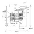
図1は、本実施の形態の発光装置100の一構成例を示す上面図であり、セラミック基板101の主表面に実装されたLEDチップ105などが樹脂モールドされる前の様子を示す。図2は、本実施の形態の発光装置100の一構成例を示す上面図であり、セラミック基板101の主表面に実装されたLEDチップ105などが樹脂モールドされ、完成パッケージとなった様子を示す。但し、樹脂モールド(後述の蛍光体含有樹脂層109)内には蛍光体が含有されており、着色されて光を吸収するので、光を透過し難く、LEDチップ105の実装面は見えない。また、後述するダム樹脂108(樹脂枠体)も光透過率が低いので、ダム樹脂108の下面は上から見えない。図2では、LEDチップ105の実装面を説明するために、これら不透明な部材を透視して記載した図面となっている。これは後述の他の実施例の図面(図5〜図10)でも同様である。図3は、図2の発光装置100のX−X’線断面図である。(overall structure)
FIG. 1 is a top view showing a configuration example of the
なお、以下では、図1,2の上下方向および左右方向を、主表面の上下方向(第1方向)および左右方向(第2方向)とする。また、図3の上側および下側を、発光装置100の上側および下側とする。さらに、セラミック基板101の主表面に垂直な方向から見たとき、すなわち図1,2に示す面視を、上面視(平面視)と呼ぶ。 In the following, the vertical direction and the horizontal direction in FIGS. 1 and 2 are defined as the vertical direction (first direction) and the horizontal direction (second direction) of the main surface. Further, the upper side and the lower side in FIG. 3 are the upper side and the lower side of the
図1〜図3に示すように、本実施の形態の発光装置100は、セラミック基板101(基板)、LEDチップ105(発光素子)、ワイヤ106(金属ワイヤ)、印刷抵抗107(保護素子)、ダム樹脂108(樹脂枠体)、および蛍光体含有樹脂層109を備えている。 As shown in FIGS. 1 to 3, the
セラミック基板101は、セラミックからなる基板である。セラミック基板101は、上面視で矩形の外形形状を有している。セラミック基板101の主表面には、LEDチップ105、ワイヤ106、印刷抵抗107、ダム樹脂108、および蛍光体含有樹脂層109が設けられている。また、セラミック基板101の主表面には、電極配線パターン102、アノード用電極ランド103、およびカソード用電極ランド104が形成されている。 The
LEDチップ105は、発光ピーク波長が450nmの青色LEDであるが、これに限るものではない。LEDチップ105としては、例えば、発光ピーク波長が390nm〜420nmの紫外(近紫外)LEDチップを用いてもよく、これにより、さらなる発光効率の向上を図ることができる。複数(本実施例では44個)のLEDチップ105が、セラミック基板101の主表面にシリコーン樹脂接着剤により固定されている。LEDチップ105は、上面視で長方形の外形形状を有している。LEDチップ105の上面には、アノード電極およびカソード電極(以下、総称する場合はチップ電極と呼ぶ)が長手方向に沿って対向するように設けられている。LEDチップ105の電気的接続は、ワイヤ106を用いたワイヤボンディングによって行われている。ワイヤ106は、例えば金からなる。 The
印刷抵抗107は、印刷されたペースト状の抵抗成分が焼成によって定着されてなる、LEDチップ105の厚みよりも薄い薄膜の抵抗素子である。印刷抵抗107は、酸化ルテニウムRuO2からなる。印刷抵抗107は、LEDチップ105に並列に接続されるように、セラミック基板101の主表面に部分的に(本実施例では3箇所:印刷抵抗107a〜107c)に形成されている。The
ダム樹脂108は、白色のシリコーン樹脂(透光性のシリコーン樹脂を母材とし、光拡散フィラーとして酸化チタンTiO2含有させたもの)からなる、光透過率が低い、または、光反射性を有する樹脂枠体である。ダム樹脂108は、LEDチップ105の実装領域を囲むように、環状に設けられている。ダム樹脂108は、上面視で4つの角部が丸みを帯びた長方形の形状を有している。なお、ダム樹脂108の材料は、上記材料に限定されるものではなく、アクリル、ウレタン、エポキシ、ポリエステル、アクリロニトリルブタジエンスチレン(ABS)、またはポリカーボネート(PC)樹脂などでもよい。また、ダム樹脂108の色も白色に限らず、例えば乳白色でもよい。樹脂を白色または乳白色に着色することで、その樹脂の光透過率を低く設定すること、または、その樹脂が光反射性を有することが可能となる。The
蛍光体含有樹脂層109は、液状のシリコーン樹脂に粒子状蛍光体を分散させたものが硬化されてなる封止樹脂層である。本実施例では、粒子状蛍光体として、赤色蛍光体SrCaAlSiN3:Eu、および、緑色蛍光体Ca3(Sc,Mg)2Si3O12:Ceを用いる。蛍光体含有樹脂層109は、LEDチップ105およびワイヤ106を覆うように、ダム樹脂108の内側に隣接して設けられている。蛍光体含有樹脂層109は、ダム樹脂108の形状に従って、上面視で4つの角部が丸みを帯びた長方形の形状を有している。セラミック基板101の主表面の上下方向が、蛍光体含有樹脂層109の短手方向となり、上記主表面の左右方向が、蛍光体含有樹脂層109の長手方向となっている。The phosphor-containing
なお、粒子状蛍光体はこれに限らず、例えば、BOSE(Ba、O、Sr、Si、Eu)などを好適に用いることができる。また、BOSEの他、SOSE(Sr、Ba、Si、O、Eu)や、YAG(Ce賦活イットリウム・アルミニウム・ガーネット)、CaAlSiN3:Eu、αサイアロン((Ca)、Si、Al、O、N、Eu)、βサイアロン(Si、Al、O、N、Eu)などを好適に用いることもできる。LEDチップ105の発光色との組合せにより、発光装置100から所定の色(色度)の発光を得るような蛍光体を用いる。Note that the particulate phosphor is not limited to this, and for example, BOSE (Ba, O, Sr, Si, Eu) or the like can be suitably used. In addition to BOSE, SOSE (Sr, Ba, Si, O, Eu), YAG (Ce activated yttrium, aluminum, garnet), CaAlSiN3 : Eu, α sialon ((Ca), Si, Al, O, N) , Eu), β sialon (Si, Al, O, N, Eu) and the like can be preferably used. A phosphor that obtains light emission of a predetermined color (chromaticity) from the
(電気回路の構成)
図4(a)に、発光装置100におけるLEDチップ105および印刷抵抗107の等価回路図を示す。(Electric circuit configuration)
FIG. 4A shows an equivalent circuit diagram of the
図4(a)に示すように、発光装置100では、44個のLEDチップ105は、11個のLEDチップ105が直列に接続されてなる直列回路部が、4個並列に接続された回路構成を有している。そして、直列回路部内のチップ配線は、A:3個直列部分、B:5個直列部分、C:3個直列部分、の3つのグループに分けられている。すなわち、3個のLEDチップ105が直列に接続されてなる直列回路部が、4個並列に接続された回路構成を有するグループAと、5個のLEDチップ105が直列に接続されてなる直列回路部が、4個並列に接続された回路構成を有するグループCと、3個のLEDチップ105が直列に接続されてなる直列回路部が、4個並列に接続された回路構成を有するグループCと、が直列に接続されているとも言える。 As shown in FIG. 4A, in the
印刷抵抗107は、分けられたグループ毎に設けられている。グループAの直列回路部に、印刷抵抗107aが並列に接続されている。グループBの直列回路部に、印刷抵抗107bが並列に接続されている。グループCの直列回路部に、印刷抵抗107cが並列に接続されている。 The
グループA〜Cの直列回路部に並列接続された3つの印刷抵抗107a〜107cは、各LEDチップ105に均等に電圧が印加されるように、それぞれの抵抗値の比が、LEDチップ105の数の比に等しくなるように設定されている。 The three
ここでは、印刷抵抗107a・107cの抵抗値をRとし、印刷抵抗107bの抵抗値をR’とすると、
R:R’=3:5
となるように、各抵抗値R,R’は調整されている。なお、各抵抗値R,R’は、各LEDチップ105発光時の無効電流が極力小さくなるようにするために、1MΩ〜10GΩの抵抗値とする。Here, assuming that the resistance value of the
R: R ′ = 3: 5
The resistance values R and R ′ are adjusted so that The resistance values R and R ′ are set to 1 MΩ to 10 GΩ in order to minimize the reactive current when the
また、LEDチップ105に対するサージ破壊の防止などの効果を奏するためには、印刷抵抗107の抵抗値は、LEDチップ105の逆バイアス方向のインピーダンスの抵抗成分よりも小さいことが好ましく、10GΩ以下であることが望ましい。さらに、発光装置として完成した後に微小領域の順方向電圧の測定を行う不良選別の検査工程で真の不良品との見分けがつく程度まで、印刷抵抗107に流れるリーク電流を抑える場合は、1MΩ以上にすることが望ましい。それゆえ、印刷抵抗107a〜107cの各抵抗値R,R’は、1MΩ〜10GΩであることが好ましい。 In order to achieve an effect such as prevention of surge destruction on the
このように、LEDチップ105をグループに分けて配置し、グループ毎に印刷抵抗107を設けることによって、11個のLEDチップ105が直列に接続されてなる直列回路部に1つの印刷抵抗107を並列に接続するよりも、直列回路部が断線した時の光出力の低下を最低限にする効果がある。 As described above, the
この効果について、比較例として図4(b)を用いて説明する。図4(b)は、11個のLEDチップ105を直列に接続し、それを4個並列に接続し、さらに並列に1個の印刷抵抗107を接続したときの等価回路図である。図4(b)に示すように、11個のLEDチップ105をグループ分けせずに直列に接続した場合、LEDチップ105が1個でもオープン不良になると、11個全部に電流が流れなくなり、11個全部が発光しなくなる。 This effect will be described with reference to FIG. 4B as a comparative example. FIG. 4B is an equivalent circuit diagram when eleven
これに対し、図4(a)に示すように、11個のLEDチップ105を3個、5個、3個直列として分けて(グループ分け)接続すると、3個直列において1個オープン不良になった場合でも、3個は電流が流れなくなるが、別のグループの8個は発光する。また、5個直列において1個オープン不良になった場合でも、5個は電流が流れなくなるが、別のグループの6個は発光する。それゆえ、図4(a)に示す構成は、図4(b)の場合のように11個全部が発光しないということがない、という顕著な効果を奏する。 On the other hand, as shown in FIG. 4 (a), when 11
また、印刷抵抗107a〜107cがLEDチップ105に並列に接続されていることによって、LEDチップ105の劣化を防止することが可能となり、長寿命化を図って信頼性を確保することが可能となる。したがって、信頼性に優れた発光装置100を提供することが可能となる。 Further, since the
(セラミック基板101の構成)
次に、セラミック基板101の主表面の構成について具体的に説明する。上述のように、セラミック基板101の主表面には、電極配線パターン102、アノード用電極ランド103、およびカソード用電極ランド104が形成されている。(Configuration of ceramic substrate 101)
Next, the configuration of the main surface of the
電極配線パターン102は、アノード用電極ランド103とカソード用電極ランド104との間において、LEDチップ105とアノード用電極ランド103とカソード用電極ランド104とを直接あるいは中継して電気的に接続するための配線パターンである。電極配線パターン102は、金(Au)からなり、回路構成に応じて配置(形成)されている。本実施例では、電極配線パターン102は、接続用配線102a・102d・102g・102j、アノード用電極102b・102e・102h(第1発光素子接続用電極)、並びに、カソード用電極102c・102f・102i(第2発光素子接続用電極)からなる。 The
アノード用電極102bおよびカソード用電極102cは、図4(a)に示したグループAのLEDチップ105の接続に対応して設けられた電極である。アノード用電極102bおよびカソード用電極102cは、各LEDチップ105と、ワイヤ106により電気的に接続される。アノード用電極102bとカソード用電極102cとは、グループAのLEDチップ105群を挟み、かつ、蛍光体含有樹脂層109の短手方向に沿って対向するように配置されている。アノード用電極102bと、カソード用電極102cと、グループAのLEDチップ105とは、1つのグループL1を構成している。 The
アノード用電極102eおよびカソード用電極102fは、図4(a)に示したグループBのLEDチップ105の接続に対応して設けられた電極である。アノード用電極102eおよびカソード用電極102fは、各LEDチップ105と、ワイヤ106により電気的に接続される。アノード用電極102eとカソード用電極102fとは、グループBのLEDチップ105群を挟み、かつ、蛍光体含有樹脂層109の短手方向に沿って対向するように配置されている。アノード用電極102eと、カソード用電極102fと、グループBのLEDチップ105とは、1つのグループL2を構成している。 The
アノード用電極102hおよびカソード用電極102iは、図4(a)に示したグループCのLEDチップ105の接続に対応して設けられた電極である。アノード用電極102hおよびカソード用電極102iは、各LEDチップ105と、ワイヤ106により電気的に接続される。アノード用電極102hとカソード用電極102iとは、グループCのLEDチップ105群を挟み、かつ、蛍光体含有樹脂層109の短手方向に沿って対応するように配置されている。アノード用電極102hと、カソード用電極102iと、グループCのLEDチップ105とは、1つのグループL3を構成している。 The
グループL1〜L3は、蛍光体含有樹脂層109の長手方向に沿って並べられている。アノード用電極102b・102e・102hは、LEDチップ105の搭載領域よりも図1中上側に並べられている。カソード用電極102c・102f・102iは、LEDチップ105の搭載領域よりも図1中下側に並べられている。 The groups L1 to L3 are arranged along the longitudinal direction of the phosphor-containing
接続用配線102a・102d・102g・102jは、アノード用電極ランド103とカソード用電極ランド104との間において、グループL1〜L3を直列に接続するための中継用配線である。接続用配線102aは、アノード用電極ランド103−アノード用電極102b間を電気的に接続する。接続用配線102dは、カソード用電極102c−アノード用電極102e間を電気的に接続する。接続用配線102gは、カソード用電極102f−アノード用電極102h間を電気的に接続する。接続用配線102jは、カソード用電極102i−カソード用電極ランド104間を電気的に接続する。接続用配線102a・102d・102g・102jは、蛍光体含有樹脂層109の短手方向に沿って、かつ、グループL1〜L3の搭載領域のそれぞれの周辺に配置されている。 The
アノード用電極ランド103およびカソード用電極ランド104は、発光装置100の外部電源と接続可能な電極である。アノード用電極ランド103およびカソード用電極ランド104は、銀(Ag)−白金(Pt)からなる。アノード用電極ランド103は、セラミック基板101の主表面の隅付近(図1中右上)に配置されている。カソード用電極ランド104は、セラミック基板101の主表面の、アノード用電極ランド103に対向する隅付近(図1中左下)に配置されている。すなわち、アノード用電極ランド103とカソード用電極ランド104とは、セラミック基板101の主表面の対角線上に、対向するように配置されている。 The
なお、接続用配線102a・102jは、アノード用電極ランド103およびカソード用電極ランド104に接続するように延設されるため、一部がダム樹脂108や蛍光体含有樹脂層109に覆われない。このため、接続用配線102a・102jにおける、ダム樹脂108や蛍光体含有樹脂層109に覆われずに露出する部分には、絶縁保護膜110を形成することが望ましい。 Note that the connection wirings 102 a and 102 j are extended so as to be connected to the
以上のように、セラミック基板101の主表面では、アノード用電極102b・102e・102hと、カソード用電極102c・102f・102iとは、対応するLEDチップ105の実装領域を挟むように配置される。また、グループL1〜L3(グループA〜C)のLEDチップ105の実装領域では、後述するように各LEDチップ105間がワイヤボンディングで直接接続することにより電気的に接続されることによって、従来用いられていた電極配線パターンが不要となる。接続用配線102a・102d・102g・102jは、グループL1〜L3(グループA〜C)のLEDチップ105群の周辺にそれぞれ配置されており、LEDチップ105群の配置内を横切らない。 As described above, on the main surface of the
よって、各LEDチップ105間の距離を縮めて、LEDチップ105の実装密度を増加することが可能となる。したがって、各LEDチップ105の発光が輝点状に見えることを軽減し、発光装置100としての面内での輝度ムラを改善すること可能となる。また、小型化することが可能となる。 Therefore, it is possible to reduce the distance between the LED chips 105 and increase the mounting density of the LED chips 105. Therefore, it is possible to reduce the light emission of each
また、アノード用電極102eおよびカソード用電極102fは、その一部が、ダム樹脂108の下部に配置されている。よって、アノード用電極102eおよびカソード用電極102fによる光の吸収を抑制することが可能となる。このように、電極配線パターン102を、できる限り樹脂枠体の下部に配置することによって、これらによる光の吸収を抑制することが可能となる。また、接続用配線を極力少なくしている。したがって、発光効率を向上することが可能となる。 Further, part of the
なお、接続用配線(特に接続用配線102d・102g)は、アノード用電極102b・102e・102h、並びに、カソード用電極102c・102f・102iに比べて幅を細くし、面積を小さくすることが好ましい。これにより、蛍光体含有樹脂層109とセラミック基板101との界面、および、蛍光体含有樹脂層109と接続用配線との界面での、発光時や非発光時の熱サイクルなどの熱的な負荷による接着特性差や熱膨張係数差による、蛍光体含有樹脂層109の剥がれを低減できる。また、この構成によって、搭載面を横断して配置される接続用配線による光ロスや、発光装置としての面内輝度ムラを低減できる。 Note that the connection wiring (particularly, the
また、アノード用電極102b・102e・102hと、カソード用電極102c・102f・102iとを、それぞれ同じ側に配置させていることによって、LEDチップ105を搭載したときのチップ電極の極性方向を同じにすることが可能となる。これにより、チップ電極の極性方向を変更せずに、すなわちLEDチップ105の向きを変えずにダイボンドすることが可能となり、LEDチップ105のダイボンド装置/工程を簡略化することが可能となる。 In addition, by arranging the
さらに、アノード用電極102b・102hは、アノード用電極102eよりも内側に位置しており、カソード用電極102c・102iは、カソード用電極102fよりも内側に位置している。このように、アノード用電極102b−カソード用電極102c間の間隔、および、アノード用電極102h−カソード用電極102iの間隔を、アノード用電極102e−カソード用電極102f間の間隔よりも狭くすることによって、アノード用電極102b・102h、並びに、カソード用電極102c・102iのワイヤボンドエリアの尤度が拡大し、ワイヤボンド作業性を向上することが可能となる。但し、電極配線パターン102による光吸収の低減を優先する場合は、この限りではない。 Furthermore, the
(LEDチップ105の配置)
次に、LEDチップ105の配置について具体的に説明する。44個のLEDチップ105は、上述した回路構成や搭載領域を考慮して、3つのグループL1〜L3に分けられている。(Arrangement of LED chip 105)
Next, the arrangement of the
グループL1では、アノード用電極102bとカソード用電極102cとの間において、直列回路部が、蛍光体含有樹脂層109の長手方向に沿って4個並列状に配置され、電気的に並列接続するように並べられている。直列回路部における各LEDチップ105は、蛍光体含有樹脂層109の短手方向に沿って3個直列状に配置され、電気的に直列接続されて並べられている。 In the group L1, four series circuit portions are arranged in parallel along the longitudinal direction of the phosphor-containing
グループL2では、アノード用電極102eとカソード用電極102fとの間において、直列回路部が、蛍光体含有樹脂層109の長手方向に沿って4個並列状に配置され、電気的に並列接続するように並べられている。直列回路部における各LEDチップ105は、蛍光体含有樹脂層109の短手方向に沿って5個直列状に配置され、電気的に直列接続されて並べられている。 In the group L2, four series circuit portions are arranged in parallel along the longitudinal direction of the phosphor-containing
グループL3では、アノード用電極102hとカソード用電極102iとの間において、直列回路部が、蛍光体含有樹脂層109の長手方向に沿って4個並列状に配置され、電気的に並列接続するように並べられている。直列回路部における各LEDチップ105は、蛍光体含有樹脂層109の短手方向に沿って3個直列状に配置され、電気的に直列接続されて並べられている。 In the group L3, four series circuit portions are arranged in parallel along the longitudinal direction of the phosphor-containing
3つのグループL1〜L3は、全体としての実装領域が小さくなるように、蛍光体含有樹脂層109の角部付近でLEDチップ105の数が少なくなるように配置されている。つまりは、グループL2は、セラミック基板101の主表面の中央付近に配置され、その両隣に蛍光体含有樹脂層109の長手方向に沿って、グループL1・L3がそれぞれ配置されている。グループL1・L3は、グループL2よりもLEDチップ105の数が少ないので、蛍光体含有樹脂層109の形状に合うように、かつ、ワイヤボンドエリアを有する電極配線パターンエリアを確保できるように、尤度を持たせて配置される。 The three groups L <b> 1 to L <b> 3 are arranged so that the number of
このように、複数のLEDチップ105を3つのグループL1〜L3に分けて配置することで、LEDチップ105の実装領域をなるべく小さな矩形内に収めることが可能となる。またこれにより、アノード用電極ランド103、およびカソード用電極ランド104を含めて、セラミック基板101上のレイアウト配置を小さくすることが可能となり、より小型の発光装置100を実現することが可能となる。 As described above, by arranging the plurality of
また、各グループL1〜L3においては、直列回路部における隣り合うLEDチップ105間は、ワイヤボンディングによって、一方のLEDチップ105のカソード電極と他方のLEDチップ105のアノード電極とがワイヤ106で直接接続されている。よって、グループL1〜L3の各内部では、各LEDチップ105間を中継する電極配線パターン102は設けられていないので、各LEDチップ105間の距離を縮めて、LEDチップ105の実装密度を増加することが可能となる。 Further, in each of the groups L1 to L3, between the
さらに、全てのLEDチップ105は、同じ向きであって、かつ、カソード電極およびアノード電極の対向方向が蛍光体含有樹脂層109の短手方向に沿うような向きで配置されている。すなわち、全てのLEDチップ105は、チップ電極の向きが揃っており、上面の長手方向が、蛍光体含有樹脂層109の短手方向に沿うように配置されている。本実施例では、アノード電極が図1中上側に位置している。これにより、チップ電極の極性方向を変更せずに、すなわちLEDチップ105の向きを変えずにダイボンドすることが可能となる。 Further, all the
(印刷抵抗107の配置)
次に、印刷抵抗107の配置について具体的に説明する。印刷抵抗107は、分けられたグループ毎(L1,L2,L3)に、印刷抵抗107a〜107cが配置されている。(Arrangement of printing resistor 107)
Next, the arrangement of the
印刷抵抗107aは、接続用配線102aとアノード用電極102eとに電気的に接続されるように形成されている。印刷抵抗107aは、アノード用電極102eと一直線状になるように配置されている。印刷抵抗107bは、カソード用電極102cとカソード用電極102fとに電気的に接続されるように形成されている。印刷抵抗107bは、接続用配線102dと一直線状になるように配置されている。印刷抵抗107cは、カソード用電極102fと接続用配線102jとに電気的に接続されるように形成されている。印刷抵抗107cは、カソード用電極102fと一直線状になるように配置されている。 The
また、印刷抵抗107a〜107cは、LEDチップ105の実装領域の周辺に配置されている。さらに、印刷抵抗107a・107cの大部分、並びに、印刷抵抗107bの一部分は、光透過率が低いダム樹脂108の下部に配置されている。 Further, the
このように、印刷抵抗107a〜107cを、できる限りダム樹脂108の下部に配置しダム樹脂108で覆い隠すことによって、印刷抵抗107a〜107cによる光吸収を最小限に抑制することが可能となる。それゆえ、発光装置100の光出力の低下を防ぐことが可能となる。 As described above, the
(ダム樹脂108の構成)
次に、ダム樹脂108の構成について具体的に説明する。(Configuration of dam resin 108)
Next, the configuration of the
図3に示すように、ダム樹脂108の断面形状は、上に凸のドーム形状(上辺<下辺)となっている。この断面形状により、LEDチップ105からの横方向、特にダム樹脂108の方向へ放射される光が、ダム樹脂108に反射される。よって、光を基板前面方向へ取り出し易くする効果がある。 As shown in FIG. 3, the cross-sectional shape of the
なお、ダム樹脂108の断面形状は、これに限らない。また、蛍光体含有樹脂層109の形成領域を最小限にするために、ダム樹脂108は、電極配線パターン102の一部、および、ワイヤ106の一部も覆うように形成されることが望ましい。 The cross-sectional shape of the
(蛍光体含有樹脂層109の構成)
次に、蛍光体含有樹脂層109の構成について具体的に説明する。(Configuration of phosphor-containing resin layer 109)
Next, the configuration of the phosphor-containing
図3に示すように、蛍光体含有樹脂層109の断面形状は、上に凸のドーム形状(上辺<下辺)となっている。つまりは、蛍光体含有樹脂層109は、外観から見ると、楕円球の一部を切り出した形状に形成されている。発光装置100では、蛍光体含有樹脂層109のドーム状をなす表面(球面)が、発光装置100の光出射面となっている。よって、上記形状の光出射面とすることにより、LEDチップ105からの光と蛍光体からの光とを効率良く取り出すことが可能となり、結果として、発光効率を向上させる効果を得ることが可能となる。 As shown in FIG. 3, the cross-sectional shape of the phosphor-containing
また、蛍光体含有樹脂層109の表面は、上述したドーム形状に限らず、蛍光体含有樹脂層の粘度の調整によって凸状の度合いが調整でき、平坦に近く、中央付近が少し凹んだ形状や、滑らかな曲面で少し凸状の形状にしてもよい。 In addition, the surface of the phosphor-containing
(製造方法)
次に、上記構成を有する発光装置100の製造方法について簡単に説明する。(Production method)
Next, a method for manufacturing the
なお、発光装置100は、複数の発光装置群からなる一体ものとして1枚の大きなセラミック基板に形成され、製造工程の最後に個々の発光装置の周囲(四方)をダイシングにて分割することで、個々の発光装置100として形成される。 In addition, the
まず、セラミック基板101の主表面に、電極配線パターン102、アノード用電極ランド103、およびカソード用電極ランド104を形成する。そして、上記セラミック基板101の主表面に、印刷抵抗107を、例えばプリント印刷により形成する。そして、上記セラミック基板101の主表面に、LEDチップ105をダイボンディングした後、ワイヤ106を用いてワイヤボンディングを行う。 First, the
続いて、上記セラミック基板101の主表面に、ダム樹脂108を形成する。具体的には、ディスペンサーにより、液状の白色シリコーン樹脂(光拡散フィラーTiO2含有)を描画することで形成する。このダム樹脂は、120℃、60分の条件で硬化させる。Subsequently, a
続いて、上記セラミック基板101の主表面に、図3に示すようなドーム状の蛍光体含有樹脂層109を形成する。具体的には、ダム樹脂108に囲まれた領域内に、ディスペンサーにより蛍光体含有樹脂層109を充填することで形成する。最後に、上記セラミック基板101を、個々の発光装置100に個片化する。これにより、発光装置100を作製し得る。この製造方法によれば、発光装置100を容易で安価に製造することが可能となる。 Subsequently, a dome-shaped phosphor-containing
なお、ダム樹脂108は、ダム樹脂108の代わりにダム樹脂108の形状に合わせて作製された成形シートを、上記セラミック基板101の主表面に張り付けて形成してもよい。成形シートは、フッ素ゴムやシリコーンゴムなどをシート状に成型したものであり、主表面に貼り付ける面側に接着シートを備えていてもよい。 The
さらに、本実施例では、ダム樹脂108を、発光装置100に必ず組み込まれるように形成しているが、成形シートをセラミック基板101の主表面に張り付けて形成する方法の場合には、発光装置100の所望の配光特性に応じて、成形シートを最終的に取り除いても構わない。 Furthermore, in this embodiment, the
また、蛍光体含有樹脂層109も、上記のような、ダム樹脂108に囲まれた領域内にディスペンサーにより蛍光体含有樹脂層109を充填して形成する方法に限らない。蛍光体含有樹脂層109は、例えば、ダム樹脂108を使用せず、金型などを使用して圧縮成型やトランスファー成型などにより、LEDチップ105や電極配線パターン102などを、蛍光体を含有した透光性樹脂にて一括封止するように形成してもよい。 Further, the phosphor-containing
上記発光装置100の製造方法では、ダム樹脂108および蛍光体含有樹脂層109を印刷抵抗107上に容易に作成することが可能となる。それゆえ、印刷抵抗107の配置領域の自由度が高くなり、印刷抵抗107を、LEDチップ105の近傍や、ダム樹脂108および蛍光体含有樹脂層109の下部に配置することが可能となる。 In the method for manufacturing the
なお、上記製造方法は、LEDチップ105を搭載した後に、ワイヤボンディングを行い、その後ダム樹脂108を形成しているが、これに限らず、先にダム樹脂108を形成し、その後LEDチップ105を搭載し、ワイヤボンディングを行ってもよい。 In the above manufacturing method, after the
ここで、上記構成を有する発光装置100の寸法の一例を挙げる。
セラミック基板101:外形サイズ12mm×15mm、厚み1mm
電極配線パターン102:幅300μm、厚み10μm
アノード用電極ランド103およびカソード用電極ランド104:直径1.4mm、直線部2mm、厚み20μm
LEDチップ105:幅240μm、長さ400μm、高さ80μm
ダム樹脂108:リング幅0.7mm、外形サイズ6.9×7.9mm、角部のR=2mm
なお、これら寸法はあくまでも一例である。Here, an example of the dimension of the light-emitting
Ceramic substrate 101: External size 12 mm × 15 mm,
Electrode wiring pattern 102:
LED chip 105: width 240 μm,
Dam resin 108: Ring width 0.7 mm, external size 6.9 × 7.9 mm, corner R = 2 mm
These dimensions are merely examples.
(変形例)
上述した発光装置100では、セラミック基板101を使用しているが、これに限らず、セラミック基板101の代わりに、例えば、金属基板表面に絶縁層を形成したメタルコア基板を使用してもよい。この場合、絶縁層は、印刷抵抗107および電極配線パターン102を形成するエリアにのみ形成し、複数のLEDチップ105を金属基板表面に直に搭載する構成とすることができる。(Modification)
In the
また、セラミック基板101の外形形状は、矩形に限定されるものではない。さらに、主表面の上下方向(第1方向)および左右方向(第2方向)は、電極配線パターン102やLEDチップ105などの相対的な位置関係によって決められるものであり、主表面の外形形状を基準として決定されるものではない。 Further, the outer shape of the
また、LEDチップ105は、上面視で長方形であったが、正方形でもよい。LEDチップ105としては、例えば、300μm四方の正方形、高さ100μmのものを用いることもできる。さらに、LEDチップ105の実装方法は、ワイヤボンドに限らず、例えばフリップチップ接合を用いてもよい(図示せず)。 Further, the
また、LEDチップ105の個数や、グループ分け、回路構成は、上述したものに限らない。例えば、上記44個のLEDチップ105は、「A:4個直列、B:4個直列、C:4個直列」などとグループ分けしても同様の効果を得ることが可能である。つまりは、複数のLEDチップ105は、2個以上のLEDチップ105が直列に接続されてなる直列回路部が、2個以上並列に接続された回路構成を有していればよい。 Further, the number, grouping, and circuit configuration of the
さらに、搭載エリアの自由度は低下するが、印刷抵抗107の代わりにツェナーダイオードを使用してもよい。この場合、直列接続部におけるLEDチップ105の直列接続数に応じて、複数のツェナーダイオードを使用することができる。 Furthermore, although the degree of freedom of the mounting area is reduced, a Zener diode may be used instead of the
次に、本発明の他の実施の形態について図面に基づいて説明する。なお、各実施の形態において説明すること以外の構成は、実施の形態1と同じである。また、説明の便宜上、各実施の形態においては、実施の形態1の図面に示した部材と同一の機能を有する部材については、同一の符号を付し、その説明を省略する。 Next, another embodiment of the present invention will be described with reference to the drawings. Configurations other than those described in each embodiment are the same as those in the first embodiment. Further, for convenience of explanation, in each embodiment, members having the same functions as those shown in the drawings of
〔実施の形態2〕
図5は、本実施の形態の発光装置200の一構成例を示す上面図である。[Embodiment 2]
FIG. 5 is a top view illustrating a configuration example of the
本実施の形態の発光装置200は、前記実施の形態1の発光装置100と比較して、電気回路の構成が異なっている。それ以外は、前記実施の形態1の発光装置100と同等の構成を有する。 The
図5に示すように、発光装置200では、7個のLEDチップ105を直線状に配列し、7個のLEDチップ105間が直列に接続された直列回路部が、14個並列に配置して並列接続された回路構成を有している。つまりは、7個直列×14個並列の直並列接続された計98個のLEDチップ105が、セラミック基板101の主表面に実装されている。 As shown in FIG. 5, in the
電極配線パターン102は、アノード用電極102k、および、カソード用電極102lからなる。アノード用電極102kおよびカソード用電極102lは、各LEDチップ105と、ワイヤ106により電気的に接続される。アノード用電極102kとカソード用電極102lとは、LEDチップ105群を挟み、かつ、蛍光体含有樹脂層109の短手方向(LEDチップ105を直線状に配列した方向)に沿って対向するように配置されている。 The
印刷抵抗107は、直列回路部に並列に接続されるように1個設けられている。つまりは、印刷抵抗107は、アノード用電極102kとカソード用電極102lとに接続されるように形成されている。印刷抵抗107は、上面視で、アノード用電極102kおよびカソード用電極102lに対し直交する方向に配置されている。 One
発光装置200では、前記実施の形態1の発光装置100と同様に、印刷抵抗107によって、LEDチップ105からなる直列回路部の断線不良を抑制する効果、および、LEDチップ105からなる直列回路部が断線したときの光出力低下を最低限にする効果を得ることが可能となる。 In the
〔実施の形態3〕
図6は、本実施の形態の発光装置300の一構成例を示す上面図である。[Embodiment 3]
FIG. 6 is a top view illustrating a configuration example of the
本実施の形態の発光装置300は、前記実施の形態1の発光装置100と比較して、LEDチップ105の実装方向(極性方向)と、それに応じたワイヤ106の配線方向とが異なっている。それ以外は、前記実施の形態1の発光装置100と同等の構成を有する。 The
図6に示すように、発光装置300では、グループL1は、4個のLEDチップ105が直列に接続されてなる直列回路部が2個並列に接続され、グループL2は、8個のLEDチップ105が直列に接続されてなる直列回路部が3個並列に接続され、グループL3は、4個のLEDチップ105が直列に接続されてなる直列回路部が2個並列に接続されている。つまりは、直並列接続された計40個のLEDチップ105が、セラミック基板101の主表面に実装されている。 As shown in FIG. 6, in the
また、各LEDチップ105は、長手方向が蛍光体含有樹脂層109の長手方向と一致するような向きで配置されている。すなわち、発光装置300のLEDチップ105は、発光装置100のLEDチップ105の配置方向から90度回転されている。このLEDチップ105の配置に応じて、ワイヤ106は斜めに配線されている。 In addition, each
発光装置300では、前記実施の形態1の発光装置100と同様の効果に加え、ダム樹脂108のサイズを小さくすることが可能となり、より点光源に近づけることが可能となる。また、発光装置300では、アノード用電極ランド103およびカソード用電極ランド104と、LEDチップ105の搭載領域との間のスペースを広く取ることができるので、LEDチップ105のボンディングが容易になるという効果がある。 In the
但し、発光装置300は、発光装置100と比較して、ワイヤ106が長くなることによるワイヤ使用量の増加が生じる。このため、全体的に見ると、発光装置300の実装方法よりも、発光装置100の実装方法の方が好ましい。 However, in the
〔実施の形態4〕
図7は、本実施の形態の発光装置400の一構成例を示す上面図である。[Embodiment 4]
FIG. 7 is a top view illustrating a configuration example of the light-emitting
本実施の形態の発光装置400は、前記実施の形態1の発光装置100と比較して、グループL2のLEDチップ105およびワイヤ106の構成が異なっている。それ以外は、前記実施の形態1の発光装置100と同等の構成を有する。 The
図7に示すように、発光装置400では、グループL2は、8個のLEDチップ105が直列に接続されてなる直列回路部が3個並列に接続されている。ゆえに、発光装置400では、直並列接続された計48個のLEDチップ105が、セラミック基板101の主表面に実装されている。グループL2の各LEDチップ105は、長手方向が蛍光体含有樹脂層109の長手方向と一致するような向きで配置されている。このLEDチップ105の配置に応じて、ワイヤ106は斜めに配線されている。 As shown in FIG. 7, in the
発光装置400では、前記実施の形態3の発光装置300のダム樹脂108と同じサイズのダム樹脂108の枠内に、より多くのLEDチップ105を実装することが可能となる。このように、所望の数のLEDチップ105が搭載されるように、グループ毎にLEDチップ105の実装方向を変えてもよい。 In the
〔実施の形態5〕
図8は、本実施の形態の発光装置500の一構成例を示す上面図である。[Embodiment 5]
FIG. 8 is a top view illustrating a configuration example of the
本実施の形態の発光装置500は、前記実施の形態1の発光装置100と比較して、発光装置100では44個のLEDチップ105が搭載されていたが、発光装置500では40個のLEDチップ105および4個のLEDチップ105’が搭載されている点が異なっている。それ以外は、前記実施の形態1の発光装置100と同等の構成を有する。 Compared with the
LEDチップ105’は、LEDチップ105よりもチップサイズが小さい(例えば、上面視で0.3×0.3mmの正方形)ものである。図8に示すように、LEDチップ105’は、全体的に見て、LEDチップ105の実装領域の4隅に配置されている。つまりは、LEDチップ105’は、蛍光体含有樹脂層109領域におけるダム樹脂108に近接した4隅に配置されている。 The
発光装置500では、蛍光体含有樹脂層109領域におけるダム樹脂108に近接した4隅のLEDチップ105’を、他に実装されたLEDチップ105よりも小さいサイズとすることで、ダム樹脂108の枠を小さくすることが可能となり、発光面積を小さくすることが可能となる。 In the
〔実施の形態6〕
図9は、本実施の形態の発光装置600の一構成例を示す上面図である。[Embodiment 6]
FIG. 9 is a top view illustrating a configuration example of the light-emitting
本実施の形態の発光装置600は、前記実施の形態1の発光装置100と比較して、ダム樹脂108および蛍光体含有樹脂層109の形状が異なっている。それ以外は、前記実施の形態1の発光装置100と同等の構成を有する。 The
図9に示すように、発光装置600では、ダム樹脂108は上面視で円環形の形状を有している。ダム樹脂108の大部分は、印刷抵抗107の上に形成されている。蛍光体含有樹脂層109は、ダム樹脂108の形状に沿って、上面視で円形の形状を有している。 As shown in FIG. 9, in the
発光装置600では、蛍光体含有樹脂層109が円形に形成されていることにより、LEDチップ105からの発光が全方向へ均一に放射され易くなる。またこれにより、発光装置600を汎用照明器具へ応用することや、その設計が容易となる。 In the
〔実施の形態7〕
図10は、本実施の形態の発光装置700の一構成例を示す上面図である。[Embodiment 7]
FIG. 10 is a top view illustrating a configuration example of the
本実施の形態の発光装置700は、前記実施の形態1の発光装置100と比較して、印刷抵抗107bの設置領域と、ダム樹脂108の設置領域とが異なっている。それ以外は、前記実施の形態1の発光装置100と同等の構成を有する。 The
図10に示すように、発光装置700では、印刷抵抗107bは、ダム樹脂108のカーブに沿った形状を有しており、ダム樹脂108の下部に配置されている。ダム樹脂108は、全ての印刷抵抗107a〜107cを覆うように太めに形成されている。 As shown in FIG. 10, in the
発光装置700では、全ての印刷抵抗107a〜107cはダム樹脂108により覆われ、他の光学特性を損なわない位置に配置されているので、印刷抵抗107a〜107cの光吸収による発光効率ロスを最小限にすることが可能となる。 In the
〔実施の形態8〕
図11は、本実施の形態の発光装置800の一構成例を示す上面図である。[Embodiment 8]
FIG. 11 is a top view illustrating a configuration example of the light-emitting
本実施の形態の発光装置800は、前記実施の形態1の発光装置100と比較して、グループL2のLEDチップ105の実装方向が異なっている。それ以外は、前記実施の形態1の発光装置100と同等の構成を有する。なお、図11では、ダム樹脂108および蛍光体含有樹脂層109を省略して記載しているが、それら部材は図2と同様に形成される。 The
図11に示すように、発光装置800では、グループL2のLEDチップ105は、カソード電極が上側に位置するような向きで配置されている。すなわち、発光装置800のグループL2のLEDチップ105は、発光装置100のグループL2のLEDチップ105の実装方向から180度回転されている。これに応じて、電極配線パターン102は、アノード用電極102eとカソード用電極102fとの配置が逆になっている。また、印刷抵抗107は、電気回路の構成は発光装置100のままで、形成領域のみが変更されている。 As shown in FIG. 11, in the
発光装置800では、グループL1とグループL2との間を接続する接続用配線102d、および、グループL2とグループL3との間を接続する接続用配線102gを、グループ間を横切るように配置させる必要がなくなるので、これら配線による光吸収ロスを軽減することが可能となる。 In the
なお、上述した実施の形態1〜8においては印刷抵抗107を必ず備えた実施例を説明してきたが、静電耐圧をそれほど必要としない用途や、各LEDチップ105自体の静電耐圧が大きい場合には、印刷抵抗107を含まない構成としてもよい。 In the above-described first to eighth embodiments, the example in which the
〔実施の形態9〕
本実施の形態では、前記実施の形態1〜8で説明した発光装置を備える電子機器について説明する。[Embodiment 9]
In this embodiment, an electronic device including the light-emitting device described in any of
例えば、裏面に電源回路を有し、放熱板と一体となった実装基板に、上記発光装置を実装してなる照明装置がある。上記発光装置のアノード用電極ランド103およびカソード用電極ランド104は、実装基板のアノード電極ランドおよびカソード電極ランドに、外部配線などにより電気的に接続される。上記発光装置の上面は、光拡散機能を備えたケース、あるいは透明なケースで覆われる。 For example, there is an illumination device in which the light-emitting device is mounted on a mounting substrate that has a power supply circuit on the back surface and is integrated with a heat sink. The
また、上記発光装置は、1つだけではなく、矩形形状のセラミック基板101の一辺が平行になるように、あるいは、矩形形状のセラミック基板101の対角線方向が一直線上になるように複数搭載し、蛍光灯型の照明装置としてもよい。なお、1つのみを搭載し、電球型の照明装置としてもよい。 Further, the light emitting device is mounted not only in one but in a plurality so that one side of the rectangular
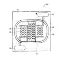
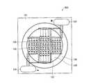
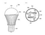
ここで、上記照明装置の具体例として、前記実施の形態1〜8で説明した発光装置を備えるLED電球の構成について説明する。図12は、LED電球900の一構成例を示す図であり、(a)は側面から見たときの外観を示し、(b)は発光装置909が搭載された搭載面を示す。 Here, as a specific example of the lighting device, a configuration of an LED bulb including the light-emitting device described in
図12に示すように、LED電球900は、口金901に固着された放熱フィン902に、搭載板904が留めネジ905によって固定されるとともに、搭載板904を覆うように散乱材入りレンズドーム903が設けられた構成を有する。口金901は、電球における、ソケットにねじ込むための金属の部分である。口金901のサイズは、E26やE17などを好適に使用できる。特に、前記実施の形態1〜8で説明した発光装置は、表面積を15mm×12mmと小さくすることが可能であるので、E17の口金が好適である。 As shown in FIG. 12, in the
搭載板904には、発光装置909が搭載される。発光装置909は、押さえピン906によって固定されている。発光装置909としては、前記実施の形態1〜8で説明した発光装置のいずれを用いてもよい。発光装置909のアノード用電極ランド103およびカソード用電極ランド104は、外部配線と電気的に接続される(アノード結線907およびカソード結線908)。 A
LED電球900は、発光装置909を備えることにより、輝度ムラが改善され、かつ、発光効率が向上されるので、非常に優れた照明装置となる。 Since the LED
さらに、複数の上記発光装置を筐体基板上にマトリクス状に配置し、面状光源を構成してもよい。この面状光源では、上記発光装置1つ1つに光の配光特性を調整する外付けレンズを設置することで、あるいは、図3に示したように蛍光体含有樹脂層109を凸状にしレンズ機能を持たせることで、光配向特性を有することが可能となる。このような面状光源をBL(バックライト)光源とした液晶表示装置を構成することができる。 Furthermore, a plurality of the light emitting devices may be arranged in a matrix on the housing substrate to constitute a planar light source. In this planar light source, each of the light emitting devices is provided with an external lens for adjusting the light distribution characteristics, or the phosphor-containing
本発明は上述した各実施形態に限定されるものではなく、請求項に示した範囲で種々の変更が可能であり、異なる実施形態にそれぞれ開示された技術的手段を適宜組み合わせて得られる実施形態についても本発明の技術的範囲に含まれる。 The present invention is not limited to the above-described embodiments, and various modifications are possible within the scope shown in the claims, and embodiments obtained by appropriately combining technical means disclosed in different embodiments. Is also included in the technical scope of the present invention.
本発明は、直並列接続された複数のLEDが基板に実装されてなる発光装置に関する分野に好適に用いることができるだけでなく、発光装置の製造方法に関する分野に好適に用いることができ、さらには、発光装置を備える電子機器などの分野にも広く用いることができる。 The present invention can be suitably used not only in a field related to a light emitting device in which a plurality of LEDs connected in series and parallel are mounted on a substrate, but also in a field related to a method of manufacturing a light emitting device, The present invention can also be widely used in the field of electronic equipment including a light emitting device.
100,200,300,400,500,600,700,800 発光装置
101 セラミック基板(基板)
102 電極配線パターン
102a・102d・102g・102j 接続用配線
102b・102e・102h アノード用電極(第1発光素子接続用電極)
102c・102f・102i カソード用電極(第2発光素子接続用電極)
103 アノード用電極ランド
104 カソード用電極ランド
105,105’ LEDチップ(発光素子)
106 ワイヤ(金属ワイヤ)
107,107a〜107c 印刷抵抗(保護素子)
108 ダム樹脂(樹脂枠体)
109 蛍光体含有樹脂層
900 LED電球
909 発光装置100, 200, 300, 400, 500, 600, 700, 800 Light-emitting
102
102c, 102f, 102i Cathode electrode (second light emitting element connection electrode)
103 Electrode land for
106 wire (metal wire)
107, 107a to 107c Printing resistance (protective element)
108 Dam resin (resin frame)
109 Phosphor-Containing
Claims (11)
Translated fromJapanese上記複数の発光素子が実装された実装領域を囲むように上記基板の主表面に環状に設けられた、低い光透過率の樹脂からなる樹脂枠体と、
上記複数の発光素子を覆うように上記樹脂枠体の内側に隣接して設けられた、蛍光体を含有する樹脂からなる蛍光体含有樹脂層とを備え、
上記基板の主表面には、該主表面内にある第1方向に沿って対向するように配置された第1発光素子接続用電極および第2発光素子接続用電極が形成され、
上記複数の発光素子は、2以上の発光素子が直列に接続されてなる直列回路部が、上記第1発光素子接続用電極と上記第2発光素子接続用電極との間において2以上並列に接続された回路構成を有し、
上記各直列回路部は、上記第1発光素子接続用電極と上記第2発光素子接続用電極との間において、上記主表面内にあり上記第1方向と直交する第2方向に沿って並べられ、
上記各直列回路部における各発光素子は、上記第1方向に沿って並べられ、
上記第1発光素子接続用電極および上記第2発光素子接続用電極は、上記樹脂枠体、上記蛍光体含有樹脂層、または、その両方の下部に配置されていることを特徴とする発光装置。In a light emitting device comprising a substrate, a plurality of light emitting elements mounted on the main surface of the substrate, and a protection element connected in parallel to the plurality of light emitting elements,
A resin frame made of a resin having a low light transmittance, provided annularly on the main surface of the substrate so as to surround a mounting region in which the plurality of light emitting elements are mounted;
A phosphor-containing resin layer made of a resin containing a phosphor, provided adjacent to the inside of the resin frame so as to cover the plurality of light emitting elements,
A first light emitting element connection electrode and a second light emitting element connection electrode are formed on the main surface of the substrate so as to face each other along the first direction in the main surface,
In the plurality of light emitting elements, two or more series light emitting elements connected in series are connected in parallel between the first light emitting element connecting electrode and the second light emitting element connecting electrode. Circuit configuration,
Each of the series circuit portions is arranged along a second direction that is in the main surface and orthogonal to the first direction, between the first light emitting element connecting electrode and the second light emitting element connecting electrode. ,
Each light emitting element in each series circuit section is arranged along the first direction,
The first light-emitting element connection electrode and the second light-emitting element connection electrode are disposed below the resin frame, the phosphor-containing resin layer, or both.
上記基板の主表面には、隣り合うグループ間を直列に接続するように配置された接続用配線が形成され、
上記保護素子は、上記グループ毎に設けられていることを特徴とする請求項1に記載の発光装置。A plurality of groups of the plurality of light emitting elements, the first light emitting element connection electrode, and the second light emitting element connection electrode are arranged along the second direction,
On the main surface of the substrate, a connection wiring is formed so as to connect adjacent groups in series,
The light emitting device according to claim 1, wherein the protection element is provided for each of the groups.
上記保護素子は、上記第1発光素子接続用電極と上記第2発光素子接続用電極とに電気的に接続されるように、上記実装領域の周辺であって、かつ、上記樹脂枠体、上記蛍光体含有樹脂層、または、その両方の下部に配置されていることを特徴とする請求項1に記載の発光装置。The protective element is a thin film printing resistor partially formed on the main surface of the substrate,
The protective element is around the mounting region and electrically connected to the first light emitting element connecting electrode and the second light emitting element connecting electrode, and the resin frame, The light-emitting device according to claim 1, wherein the light-emitting device is disposed under the phosphor-containing resin layer or both of them.
上記各保護素子は、対応するグループにおける上記第1発光素子接続用電極と上記第2発光素子接続用電極とに電気的に接続されるように、上記実装領域の周辺であって、かつ、上記樹脂枠体、上記蛍光体含有樹脂層、または、その両方の下部に配置されていることを特徴とする請求項2に記載の発光装置。Each of the protective elements is a thin film printing resistor partially formed on the main surface of the substrate,
Each of the protection elements is around the mounting region so as to be electrically connected to the first light emitting element connection electrode and the second light emitting element connection electrode in the corresponding group, and The light emitting device according to claim 2, wherein the light emitting device is disposed below the resin frame, the phosphor-containing resin layer, or both.
上記複数の発光素子は全て、同じ向きであって、かつ、上記カソード電極および上記アノード電極の対向方向が上記第1方向に沿うような向きで配置されていることを特徴とする請求項4に記載の発光装置。The cathode electrode and the anode electrode of each light emitting element are arranged to face each other,
5. The plurality of light emitting elements are all arranged in the same direction and in such a direction that opposing directions of the cathode electrode and the anode electrode are along the first direction. The light-emitting device of description.
上記複数の発光素子は全て、同じ向きであって、かつ、上記カソード電極および上記アノード電極の対向方向が上記第2方向に沿うような向きで配置されていることを特徴とする請求項4に記載の発光装置。The cathode electrode and the anode electrode of each light emitting element are arranged to face each other,
5. The plurality of light emitting elements are all arranged in the same direction and in such a direction that opposing directions of the cathode electrode and the anode electrode are along the second direction. The light-emitting device of description.
Priority Applications (11)
| Application Number | Priority Date | Filing Date | Title |
|---|---|---|---|
| JP2010012486AJP2011151268A (en) | 2010-01-22 | 2010-01-22 | Light emitting device |
| CN201410680688.2ACN104465633B (en) | 2010-01-22 | 2011-01-20 | Light-emitting device |
| CN201110025234.8ACN102157506B (en) | 2010-01-22 | 2011-01-20 | Light emitting device |
| CN201410234294.4ACN104091798B (en) | 2010-01-22 | 2011-01-20 | LED electric bulb |
| US13/011,124US8421094B2 (en) | 2010-01-22 | 2011-01-21 | Light emitting device |
| US13/799,373US8723195B2 (en) | 2010-01-22 | 2013-03-13 | Light emitting device with plurality of LED chips and/or electrode wiring pattern |
| US14/217,701US9093357B2 (en) | 2010-01-22 | 2014-03-18 | Light emitting device |
| US14/627,239US9312304B2 (en) | 2010-01-22 | 2015-02-20 | LED illuminating device comprising light emitting device including LED chips on single substrate |
| US14/674,624US9425236B2 (en) | 2010-01-22 | 2015-03-31 | Light emitting device |
| US15/187,945US9679942B2 (en) | 2010-01-22 | 2016-06-21 | Light emitting device |
| US15/587,759US9966367B2 (en) | 2010-01-22 | 2017-05-05 | Light emitting device |
Applications Claiming Priority (1)
| Application Number | Priority Date | Filing Date | Title |
|---|---|---|---|
| JP2010012486AJP2011151268A (en) | 2010-01-22 | 2010-01-22 | Light emitting device |
Related Child Applications (1)
| Application Number | Title | Priority Date | Filing Date |
|---|---|---|---|
| JP2013165596ADivisionJP5844317B2 (en) | 2013-08-08 | 2013-08-08 | LED bulb |
Publications (1)
| Publication Number | Publication Date |
|---|---|
| JP2011151268Atrue JP2011151268A (en) | 2011-08-04 |
Family
ID=44308296
Family Applications (1)
| Application Number | Title | Priority Date | Filing Date |
|---|---|---|---|
| JP2010012486APendingJP2011151268A (en) | 2010-01-22 | 2010-01-22 | Light emitting device |
Country Status (3)
| Country | Link |
|---|---|
| US (7) | US8421094B2 (en) |
| JP (1) | JP2011151268A (en) |
| CN (3) | CN104465633B (en) |
Cited By (23)
| Publication number | Priority date | Publication date | Assignee | Title |
|---|---|---|---|---|
| JP2013065692A (en)* | 2011-09-16 | 2013-04-11 | Fuji Xerox Co Ltd | Surface emitting semiconductor laser, surface emitting semiconductor laser device, optical transmission device and information processing unit |
| JP2013084586A (en)* | 2011-09-30 | 2013-05-09 | Ichikoh Ind Ltd | Semiconductor type light source for vehicular lamp fitting, unit for the same, and vehicular lamp fitting |
| JP2013098219A (en)* | 2011-10-28 | 2013-05-20 | Nichia Chem Ind Ltd | Light-emitting device and manufacturing method of the same |
| JP2013118284A (en)* | 2011-12-02 | 2013-06-13 | Hitachi Appliances Inc | Light emitting diode module |
| WO2013094700A1 (en)* | 2011-12-20 | 2013-06-27 | シチズンホールディングス株式会社 | Led module |
| KR101287544B1 (en)* | 2012-01-27 | 2013-07-19 | 금호전기주식회사 | Cob type led package |
| WO2014122971A1 (en)* | 2013-02-06 | 2014-08-14 | シャープ株式会社 | Light-emitting device and method for manufacturing light-emitting device |
| WO2014168325A1 (en)* | 2013-04-09 | 2014-10-16 | 주식회사 굿엘이디 | High-efficiency cob led package |
| JP2014220154A (en)* | 2013-05-09 | 2014-11-20 | 東芝ライテック株式会社 | Lighting device |
| JP2015103733A (en)* | 2013-11-27 | 2015-06-04 | 豊田合成株式会社 | Light emitting device |
| KR101563281B1 (en) | 2015-03-26 | 2015-10-26 | 주식회사 엘앤에스엘이디 | Ac cob type led |
| JP2016524322A (en)* | 2013-05-08 | 2016-08-12 | エルジー イノテック カンパニー リミテッド | Light emitting element |
| US9577153B2 (en) | 2012-02-20 | 2017-02-21 | Sharp Kabushiki Kaisha | Light emission device and illumination device |
| JP2018503984A (en)* | 2015-05-27 | 2018-02-08 | 深▲セン▼市華星光電技術有限公司 | Light emitting device assembly structure |
| JPWO2016194876A1 (en)* | 2015-05-29 | 2018-03-15 | シチズン電子株式会社 | Light emitting device and manufacturing method thereof |
| JP2018157163A (en)* | 2017-03-21 | 2018-10-04 | 島根県 | Semiconductor light-emitting module and manufacturing method thereof |
| JP2018537850A (en)* | 2015-11-20 | 2018-12-20 | 福建中科芯源光電科技有限公司 | Die bonding substrate, high density integrated COB white light source, and manufacturing method thereof |
| JP2019220399A (en)* | 2018-06-21 | 2019-12-26 | シャープ株式会社 | Luminaire and projector |
| KR20200088954A (en)* | 2019-01-15 | 2020-07-24 | 삼성디스플레이 주식회사 | Display device |
| JP2020184585A (en)* | 2019-05-08 | 2020-11-12 | シーシーエス株式会社 | Led light-emitting device |
| JP2021036597A (en)* | 2020-10-28 | 2021-03-04 | 日亜化学工業株式会社 | Light-emitting device |
| CN113474904A (en)* | 2019-02-27 | 2021-10-01 | 欧司朗光电半导体有限公司 | Device and method for replacing at least one chip |
| WO2023074285A1 (en)* | 2021-10-27 | 2023-05-04 | ソニーセミコンダクタソリューションズ株式会社 | Light emitting element array |
Families Citing this family (72)
| Publication number | Priority date | Publication date | Assignee | Title |
|---|---|---|---|---|
| JP5623062B2 (en) | 2009-11-13 | 2014-11-12 | シャープ株式会社 | Light emitting device and manufacturing method thereof |
| JP2011151268A (en) | 2010-01-22 | 2011-08-04 | Sharp Corp | Light emitting device |
| JP5612991B2 (en)* | 2010-09-30 | 2014-10-22 | シャープ株式会社 | LIGHT EMITTING DEVICE AND LIGHTING DEVICE HAVING THE SAME |
| JP5236843B1 (en)* | 2011-10-11 | 2013-07-17 | パナソニック株式会社 | LIGHT EMITTING DEVICE AND LIGHTING DEVICE USING THE SAME |
| US8662708B2 (en)* | 2011-10-18 | 2014-03-04 | Uniled Lighting Taiwan Inc. | Double heat sink LED tube |
| EP2634480B1 (en) | 2011-11-21 | 2016-09-28 | Panasonic Intellectual Property Management Co., Ltd. | Light emitting apparatus and illuminating apparatus |
| WO2013088619A1 (en)* | 2011-12-16 | 2013-06-20 | パナソニック株式会社 | Light-emitting module, and illumination light source and illumination device using same |
| US8759847B2 (en)* | 2011-12-22 | 2014-06-24 | Bridgelux, Inc. | White LED assembly with LED string and intermediate node substrate terminals |
| US8876334B2 (en)* | 2012-01-16 | 2014-11-04 | Paragon Semiconductor Lighting Technology Co., Ltd. | Light-mixing multichip package structure |
| AT14124U1 (en)* | 2012-02-13 | 2015-04-15 | Tridonic Jennersdorf Gmbh | LED module with Flächenverguß |
| JP5992695B2 (en)* | 2012-02-29 | 2016-09-14 | スタンレー電気株式会社 | Semiconductor light emitting element array and vehicle lamp |
| RU2014144356A (en)* | 2012-04-05 | 2016-05-27 | Конинклейке Филипс Н.В. | LIGHT-RADIATING STRUCTURE BASED ON LIGHT-RADIATING DEVICES |
| US9171826B2 (en) | 2012-09-04 | 2015-10-27 | Micron Technology, Inc. | High voltage solid-state transducers and solid-state transducer arrays having electrical cross-connections and associated systems and methods |
| CN102829445A (en)* | 2012-09-04 | 2012-12-19 | 苏州金科信汇光电科技有限公司 | Integrated LED (light-emitting diode) with balancing mechanism and manufacturing process thereof |
| CN102931300B (en)* | 2012-11-20 | 2017-02-08 | 无锡华润华晶微电子有限公司 | Method for manufacturing back metallic reflector array in manufacturing process of GaN-based LED |
| JP5979494B2 (en)* | 2012-12-20 | 2016-08-24 | パナソニックIpマネジメント株式会社 | Lighting device and light emitting module |
| JP6023660B2 (en)* | 2013-05-30 | 2016-11-09 | スタンレー電気株式会社 | Semiconductor light emitting device and semiconductor light emitting device |
| CN105453284B (en)* | 2013-07-09 | 2018-03-20 | Psi株式会社 | Microminiature light emitting diode electrode assemblie and its manufacture method |
| KR101429095B1 (en)* | 2013-07-09 | 2014-08-12 | 피에스아이 주식회사 | LED lamps with nano-scale LED electrode assembly |
| JP6301097B2 (en)* | 2013-10-01 | 2018-03-28 | シチズン電子株式会社 | Semiconductor light emitting device |
| JP2015138704A (en)* | 2014-01-23 | 2015-07-30 | スリーエム イノベイティブ プロパティズ カンパニー | light-emitting element module |
| JP6203147B2 (en)* | 2014-01-29 | 2017-09-27 | シャープ株式会社 | Light emitting device |
| DE102015009454B4 (en)* | 2014-07-29 | 2025-05-08 | Tdk-Micronas Gmbh | Electrical component |
| JP6372257B2 (en)* | 2014-08-29 | 2018-08-15 | 東芝ライテック株式会社 | LIGHT EMITTING MODULE FOR VEHICLE, LIGHTING DEVICE FOR VEHICLE, AND VEHICLE LIGHT |
| JP6519135B2 (en)* | 2014-09-26 | 2019-05-29 | 日亜化学工業株式会社 | Light emitting device and substrate for light emitting device |
| US9853197B2 (en) | 2014-09-29 | 2017-12-26 | Bridgelux, Inc. | Light emitting diode package having series connected LEDs |
| US20160095409A1 (en)* | 2014-10-01 | 2016-04-07 | Prior Company Limited | Light curing structure of artistic nail polish curing apparatus |
| USD766196S1 (en) | 2014-10-06 | 2016-09-13 | Citizen Electronics Co., Ltd. | Light-emitting diode |
| USD762182S1 (en) | 2014-10-06 | 2016-07-26 | Citizen Electronics Co., Ltd. | Light-emitting diode |
| KR102381317B1 (en)* | 2014-10-30 | 2022-04-01 | 삼성디스플레이 주식회사 | Backlight unit |
| WO2016084437A1 (en)* | 2014-11-28 | 2016-06-02 | シャープ株式会社 | Light emitting device and lighting device |
| JP6395859B2 (en)* | 2014-12-05 | 2018-09-26 | シャープ株式会社 | Light emitting device and lighting apparatus |
| CN104505454B (en)* | 2014-12-06 | 2017-06-20 | 深圳市格天光电有限公司 | Specular removal street lamp flip COB light source and its production technology |
| JP6476857B2 (en)* | 2014-12-29 | 2019-03-06 | 日亜化学工業株式会社 | Light emitting device |
| JPWO2016147484A1 (en)* | 2015-03-13 | 2018-01-18 | シャープ株式会社 | Light emitting device |
| EP3279939B1 (en)* | 2015-04-02 | 2019-12-18 | Sharp Kabushiki Kaisha | Light-emitting device |
| USD786808S1 (en) | 2015-05-20 | 2017-05-16 | Citizen Electronics Co., Ltd. | Light-emitting diode |
| CN107690714B (en)* | 2015-08-24 | 2020-03-27 | 京瓷株式会社 | Substrate for mounting light-emitting element, light-emitting device, and light-emitting module |
| US20170059116A1 (en)* | 2015-08-31 | 2017-03-02 | Osram Sylvania Inc. | Led array within asymmetric cavity having reflective and non-reflective regions |
| US20170059115A1 (en)* | 2015-08-31 | 2017-03-02 | Osram Sylvania Inc. | Led array on partially reflective substrate within dam having reflective and non-reflective regions |
| JP2017050445A (en)* | 2015-09-03 | 2017-03-09 | パナソニックIpマネジメント株式会社 | Light-emitting device and luminaire |
| USD789308S1 (en)* | 2015-10-23 | 2017-06-13 | Citizen Electronics Co., Ltd. | Light-emitting diode |
| USD791089S1 (en)* | 2015-10-23 | 2017-07-04 | Citizen Electronics Co., Ltd. | Light-emitting diode |
| CN105470246B (en)* | 2015-12-21 | 2016-09-28 | 福建中科芯源光电科技有限公司 | The dual pathways heat conduction encapsulating structure of solid state fluorescence body integrated optical source and method for packing |
| KR20170104031A (en) | 2016-03-03 | 2017-09-14 | 삼성전자주식회사 | Package substrate and semiconductor light emitting device package |
| US20170268752A1 (en)* | 2016-03-17 | 2017-09-21 | Amerillum LLC | Illumination Systems with LED-Based Extension Light Source |
| DE102016105777A1 (en)* | 2016-03-30 | 2017-10-05 | Osram Opto Semiconductors Gmbh | module |
| CN105805616A (en)* | 2016-05-17 | 2016-07-27 | 复旦大学 | LED area light source modules capable of being spliced in array |
| EP3467887B1 (en)* | 2016-05-24 | 2022-01-26 | Citizen Electronics Co., Ltd. | Led lighting device and method for manufacturing led lighting device |
| US10596388B2 (en) | 2016-09-21 | 2020-03-24 | Epistar Corporation | Therapeutic light-emitting module |
| JP6776855B2 (en)* | 2016-12-06 | 2020-10-28 | 日亜化学工業株式会社 | Light emitting device |
| JP2018121038A (en)* | 2017-01-27 | 2018-08-02 | パナソニックIpマネジメント株式会社 | Mounting board, light emitting device, and lighting device |
| JP6411572B1 (en)* | 2017-03-29 | 2018-10-24 | Hoya Candeo Optronics株式会社 | Light emitting device and light irradiation device including the light emitting device |
| CN107246553A (en)* | 2017-07-30 | 2017-10-13 | 黄琴 | One kind can directly exchange driving LED pieces |
| JP6916525B2 (en)* | 2018-02-06 | 2021-08-11 | 株式会社ブイ・テクノロジー | LED display manufacturing method |
| KR102766461B1 (en)* | 2018-08-20 | 2025-02-13 | 삼성전자주식회사 | Display appartus and manufacuring mehtod thereof |
| CN111211106B (en)* | 2018-11-21 | 2025-09-05 | 长鑫存储技术有限公司 | Wiring layer structure and preparation method thereof, and pad structure |
| US20210074880A1 (en)* | 2018-12-18 | 2021-03-11 | Bolb Inc. | Light-output-power self-awareness light-emitting device |
| JP7113390B2 (en)* | 2018-12-21 | 2022-08-05 | 豊田合成株式会社 | Method for manufacturing light emitting device |
| CN109994459B (en)* | 2019-04-08 | 2023-12-29 | 东莞市铱源光电科技有限公司 | Method and structure for full-color light distribution of high-integration LED chip module |
| CN110098170B (en)* | 2019-04-12 | 2020-01-14 | 潮州三环(集团)股份有限公司 | Ceramic packaging substrate combined plate for improving electrolytic plating uniformity |
| JP7149899B2 (en)* | 2019-06-07 | 2022-10-07 | 三菱電機株式会社 | semiconductor equipment |
| WO2020244784A1 (en) | 2019-06-07 | 2020-12-10 | Jenoptik Optical Systems Gmbh | Led illumination apparatus |
| US11271032B2 (en)* | 2019-06-20 | 2022-03-08 | Samsung Display Co., Ltd. | Display device |
| CN110783235A (en)* | 2019-11-04 | 2020-02-11 | 黄倩倩 | A LED wafer detection and picking equipment based on photosensitive elements |
| CN111092140B (en)* | 2019-11-27 | 2021-12-14 | 安徽锐拓电子有限公司 | LED light source and display device |
| CN115280520B (en)* | 2020-03-10 | 2023-06-30 | 西铁城电子株式会社 | light emitting device |
| CN111998252A (en)* | 2020-09-02 | 2020-11-27 | 杭州昀芯光电科技有限公司 | A kind of LED patch cord lamp with parallel and series structure |
| WO2022120605A1 (en)* | 2020-12-08 | 2022-06-16 | 京东方科技集团股份有限公司 | Array substrate, light emitting substrate, and display device |
| KR20220145969A (en)* | 2021-04-22 | 2022-11-01 | 삼성디스플레이 주식회사 | Display device and tiled display device |
| JP2024527350A (en) | 2021-07-09 | 2024-07-24 | ルミレッズ リミテッド ライアビリティ カンパニー | LED module and vehicle headlight comprising such an LED module |
| CN118968934A (en)* | 2024-09-26 | 2024-11-15 | 佛山市国星光电股份有限公司 | Backlight board, backlight module and display panel |
Citations (7)
| Publication number | Priority date | Publication date | Assignee | Title |
|---|---|---|---|---|
| JPS5684368U (en)* | 1979-11-29 | 1981-07-07 | ||
| JPH07273371A (en)* | 1994-03-31 | 1995-10-20 | Okaya Electric Ind Co Ltd | Light-emitting diode driving circuit |
| JP2007250899A (en)* | 2006-03-16 | 2007-09-27 | Matsushita Electric Ind Co Ltd | LIGHT EMITTING MODULE AND DISPLAY DEVICE AND LIGHTING DEVICE USING THE SAME |
| WO2008069204A1 (en)* | 2006-12-04 | 2008-06-12 | Alps Electric Co., Ltd. | Light emitting device and projector |
| JP2009135485A (en)* | 2007-11-07 | 2009-06-18 | Mitsubishi Chemicals Corp | Semiconductor light emitting device and manufacturing method thereof |
| JP2009164157A (en)* | 2007-12-28 | 2009-07-23 | Nichia Corp | Light-emitting device |
| JP2009231148A (en)* | 2008-03-24 | 2009-10-08 | Toshiba Lighting & Technology Corp | Illuminating device |
Family Cites Families (108)
| Publication number | Priority date | Publication date | Assignee | Title |
|---|---|---|---|---|
| JPS5378048A (en) | 1976-12-22 | 1978-07-11 | Hitachi Ltd | Glass coated thick film resistor |
| JPS5918454A (en) | 1982-07-22 | 1984-01-30 | Yuji Takayama | Carrier gas controlling apparatus for on-column capillary chromatograph |
| JPS60179057U (en) | 1984-05-04 | 1985-11-28 | 株式会社 シチズン電子 | light emitting diode |
| JPS62172164A (en) | 1986-01-27 | 1987-07-29 | 松下冷機株式会社 | Operation controller for refrigerator |
| JPS62172164U (en) | 1986-04-23 | 1987-10-31 | ||
| JPS63180957A (en) | 1987-01-22 | 1988-07-26 | Canon Inc | electrophotographic photoreceptor |
| JPS63180957U (en) | 1987-05-14 | 1988-11-22 | ||
| JPH03156708A (en) | 1989-11-15 | 1991-07-04 | Pioneer Electron Corp | Magnetic head |
| JP2772166B2 (en) | 1991-07-25 | 1998-07-02 | ローム株式会社 | LED light source device |
| JPH0545812A (en) | 1991-08-16 | 1993-02-26 | Konica Corp | Silver halide color photographic sensitive material |
| JP2729899B2 (en) | 1993-03-08 | 1998-03-18 | スタンレー電気株式会社 | LED lights for vehicles |
| JPH07122786A (en) | 1993-10-27 | 1995-05-12 | Victor Co Of Japan Ltd | Led array device |
| JP3156826B2 (en) | 1995-03-07 | 2001-04-16 | 矢崎総業株式会社 | Automatic production equipment for wires with terminals |
| JP3156708B1 (en) | 1995-06-14 | 2001-04-16 | 松下電器産業株式会社 | Data transmission device |
| JPH1098244A (en) | 1996-09-19 | 1998-04-14 | Taiyo Yuden Co Ltd | Thick-film circuit board and its manufacture |
| US6008582A (en) | 1997-01-27 | 1999-12-28 | Dai Nippon Printing Co., Ltd. | Plasma display device with auxiliary partition walls, corrugated, tiered and pigmented walls |
| JPH11191634A (en) | 1997-12-25 | 1999-07-13 | Sanken Electric Co Ltd | Semiconductor light-emitting device |
| JPH11298041A (en) | 1998-04-15 | 1999-10-29 | Toyoda Gosei Co Ltd | Group iii nitride semiconductor light-emitting element and light source device |
| JP4156072B2 (en) | 1998-04-23 | 2008-09-24 | アビックス株式会社 | LED collective lamp for AC power supply |
| JP2001237462A (en) | 2000-02-22 | 2001-08-31 | Sanyo Electric Co Ltd | Light-emitting device |
| JP2001351404A (en) | 2000-04-06 | 2001-12-21 | Kansai Tlo Kk | Surface light emitting device using light emitting diode |
| JP2002094121A (en) | 2000-09-19 | 2002-03-29 | Toshiba Electronic Engineering Corp | Semiconductor light emitting device |
| US6583550B2 (en)* | 2000-10-24 | 2003-06-24 | Toyoda Gosei Co., Ltd. | Fluorescent tube with light emitting diodes |
| JP3863028B2 (en) | 2001-02-06 | 2006-12-27 | 常盤電業株式会社 | Luminescent body and signal lamp |
| US6498372B2 (en)* | 2001-02-16 | 2002-12-24 | International Business Machines Corporation | Conductive coupling of electrical structures to a semiconductor device located under a buried oxide layer |
| JP2002299801A (en) | 2001-03-30 | 2002-10-11 | Kyocera Corp | Circuit board |
| JP2002304903A (en) | 2001-04-04 | 2002-10-18 | Matsushita Electric Works Ltd | lighting equipment |
| JP4899249B2 (en) | 2001-04-05 | 2012-03-21 | 旭硝子株式会社 | Lead-free glass, glass ceramic composition and glass paste |
| JP3960053B2 (en) | 2002-01-18 | 2007-08-15 | 松下電器産業株式会社 | Semiconductor light emitting device and light emitting device for illumination using the same |
| JP2003273406A (en) | 2002-03-20 | 2003-09-26 | Idec Izumi Corp | Light emitting element mounting substrate |
| JP4310086B2 (en) | 2002-08-01 | 2009-08-05 | 株式会社日立製作所 | Engine electronics |
| JP2004087812A (en) | 2002-08-27 | 2004-03-18 | Sanyo Electric Co Ltd | Light emitting device |
| US7244965B2 (en) | 2002-09-04 | 2007-07-17 | Cree Inc, | Power surface mount light emitting die package |
| JP4030463B2 (en) | 2003-05-20 | 2008-01-09 | 三洋電機株式会社 | LED light source and manufacturing method thereof |
| EP1658642B1 (en)* | 2003-08-28 | 2014-02-26 | Panasonic Corporation | Semiconductor light emitting device, light emitting module, lighting apparatus, display element and manufacturing method of semiconductor light emitting device |
| US6942360B2 (en) | 2003-10-01 | 2005-09-13 | Enertron, Inc. | Methods and apparatus for an LED light engine |
| JP4254669B2 (en) | 2004-09-07 | 2009-04-15 | 豊田合成株式会社 | Light emitting device |
| JP2006080383A (en) | 2004-09-10 | 2006-03-23 | Matsushita Electric Ind Co Ltd | Light emitting device and temperature detection method thereof |
| JP4083720B2 (en)* | 2004-09-17 | 2008-04-30 | シャープ株式会社 | Optical pickup device |
| KR200373718Y1 (en) | 2004-09-20 | 2005-01-21 | 주식회사 티씨오 | High Brightness LED With Protective Function of Electrostatic Damage |
| US9070850B2 (en) | 2007-10-31 | 2015-06-30 | Cree, Inc. | Light emitting diode package and method for fabricating same |
| US9793247B2 (en) | 2005-01-10 | 2017-10-17 | Cree, Inc. | Solid state lighting component |
| US7821023B2 (en) | 2005-01-10 | 2010-10-26 | Cree, Inc. | Solid state lighting component |
| JP2006222412A (en)* | 2005-01-17 | 2006-08-24 | Citizen Electronics Co Ltd | Light emitting apparatus |
| JP4857633B2 (en) | 2005-07-20 | 2012-01-18 | スタンレー電気株式会社 | LED light source |
| JP2007116095A (en) | 2005-07-25 | 2007-05-10 | Matsushita Electric Works Ltd | Light-emitting apparatus |
| CN1909238B (en) | 2005-08-03 | 2010-11-03 | 三星电机株式会社 | Light emitting device having protection element and method of manufacturing the light emitting device |
| EP1750309A3 (en)* | 2005-08-03 | 2009-07-29 | Samsung Electro-mechanics Co., Ltd | Light emitting device having protection element |
| US20070090488A1 (en)* | 2005-10-24 | 2007-04-26 | Tyntek Corporation | High-efficiency matrix-type LED device |
| JP2007123789A (en) | 2005-10-31 | 2007-05-17 | Mitsumi Electric Co Ltd | Electronic component mounting structure of electronic module |
| TWM289865U (en) | 2005-11-08 | 2006-04-21 | Lighthouse Technology Co Ltd | Sectional light emitting diode backlight unit |
| WO2007061033A1 (en) | 2005-11-28 | 2007-05-31 | Sharp Kabushiki Kaisha | Illuminating device and method for manufacturing same |
| CN101852349B (en) | 2005-12-22 | 2012-08-29 | 松下电器产业株式会社 | Lighting apparatus with led |
| JP4049186B2 (en) | 2006-01-26 | 2008-02-20 | ソニー株式会社 | Light source device |
| TWI284433B (en) | 2006-02-23 | 2007-07-21 | Novalite Optronics Corp | Light emitting diode package and fabricating method thereof |
| US20100084683A1 (en) | 2006-02-23 | 2010-04-08 | Novalite Optronics Corp. | Light emitting diode package and fabricating method thereof |
| CN100449202C (en) | 2006-02-28 | 2009-01-07 | 周维平 | Festoon lighting |
| JP2007294547A (en)* | 2006-04-21 | 2007-11-08 | Sharp Corp | Semiconductor light emitting device |
| JP4975370B2 (en) | 2006-05-16 | 2012-07-11 | 株式会社フジクラ | Light emitting device |
| CN100392855C (en)* | 2006-05-19 | 2008-06-04 | 广州南科集成电子有限公司 | U-groove LED integrated chip and manufacturing method |
| JP2007324205A (en) | 2006-05-30 | 2007-12-13 | Toyoda Gosei Co Ltd | Light emitting device |
| JP2007332009A (en) | 2006-06-19 | 2007-12-27 | Noritake Co Ltd | Lead-free insulating glass composition and lead-free insulating glass paste |
| JP2008004844A (en) | 2006-06-23 | 2008-01-10 | Sharp Corp | Light emitting device and manufacturing method thereof |
| KR100809263B1 (en) | 2006-07-10 | 2008-02-29 | 삼성전기주식회사 | Direct type backlight device |
| JP5555971B2 (en) | 2006-07-18 | 2014-07-23 | 日亜化学工業株式会社 | Linear light-emitting device and planar light-emitting device using the same |
| JP2008041290A (en) | 2006-08-02 | 2008-02-21 | Akita Denshi Systems:Kk | LIGHTING DEVICE AND MANUFACTURING METHOD THEREOF |
| JP2008060129A (en) | 2006-08-29 | 2008-03-13 | Nec Lighting Ltd | Full-color light-emitting diode |
| JP4882634B2 (en) | 2006-09-26 | 2012-02-22 | 日亜化学工業株式会社 | Light emitting device |
| JP2008085109A (en) | 2006-09-28 | 2008-04-10 | Matsushita Electric Ind Co Ltd | Light emitting diode mounting board |
| EP1928026A1 (en) | 2006-11-30 | 2008-06-04 | Toshiba Lighting & Technology Corporation | Illumination device with semiconductor light-emitting elements |
| JP2008235719A (en) | 2007-03-22 | 2008-10-02 | Toshiba Lighting & Technology Corp | Lighting device |
| EP2111640B1 (en) | 2007-01-22 | 2019-05-08 | Cree, Inc. | Fault tolerant light emitter and method of fabricating the same |
| JP4753904B2 (en) | 2007-03-15 | 2011-08-24 | シャープ株式会社 | Light emitting device |
| JP5181505B2 (en) | 2007-03-22 | 2013-04-10 | 東芝ライテック株式会社 | Light emitting device |
| JP5089212B2 (en) | 2007-03-23 | 2012-12-05 | シャープ株式会社 | LIGHT EMITTING DEVICE, LED LAMP USING THE SAME, AND METHOD FOR MANUFACTURING LIGHT EMITTING DEVICE |
| JP5138679B2 (en)* | 2007-05-08 | 2013-02-06 | シャープ株式会社 | Active matrix substrate, liquid crystal panel, liquid crystal display unit, liquid crystal display device, television receiver |
| JP2009040884A (en) | 2007-08-09 | 2009-02-26 | Hitachi Ltd | RESIN COMPOSITION FOR LIGHT REFLECTION PART FORMATION, WIRING BOARD HAVING FILM OF THE COMPOSITION, ITS MANUFACTURING METHOD, OPTICAL SEMICONDUCTOR PACKAGE, AND LIGHTING DEVICE |
| JP2009059883A (en) | 2007-08-31 | 2009-03-19 | Toyoda Gosei Co Ltd | Light emitting device |
| CN101388161A (en)* | 2007-09-14 | 2009-03-18 | 科锐香港有限公司 | LED surface mounting device and LED display incorporating the same |
| JP5538671B2 (en) | 2007-09-19 | 2014-07-02 | シャープ株式会社 | Light emitting device and LED lamp |
| JP5329787B2 (en) | 2007-09-28 | 2013-10-30 | パナソニック株式会社 | Mounting board and LED module |
| US10256385B2 (en) | 2007-10-31 | 2019-04-09 | Cree, Inc. | Light emitting die (LED) packages and related methods |
| US8866169B2 (en) | 2007-10-31 | 2014-10-21 | Cree, Inc. | LED package with increased feature sizes |
| US9172012B2 (en) | 2007-10-31 | 2015-10-27 | Cree, Inc. | Multi-chip light emitter packages and related methods |
| US9082921B2 (en) | 2007-10-31 | 2015-07-14 | Cree, Inc. | Multi-die LED package |
| US9666762B2 (en) | 2007-10-31 | 2017-05-30 | Cree, Inc. | Multi-chip light emitter packages and related methods |
| TWI378573B (en) | 2007-10-31 | 2012-12-01 | Young Lighting Technology Corp | Light emitting diode package |
| JP5344809B2 (en)* | 2007-11-21 | 2013-11-20 | アルパイン株式会社 | Backlight device |
| JP2009158872A (en) | 2007-12-27 | 2009-07-16 | Toshiba Lighting & Technology Corp | Lighting device |
| US8049237B2 (en)* | 2007-12-28 | 2011-11-01 | Nichia Corporation | Light emitting device |
| JP2009206383A (en) | 2008-02-29 | 2009-09-10 | Sharp Corp | Led module and led lighting device with the same |
| JP5056520B2 (en) | 2008-03-21 | 2012-10-24 | 東芝ライテック株式会社 | Lighting device |
| JP5355030B2 (en) | 2008-04-24 | 2013-11-27 | シチズンホールディングス株式会社 | LED light source and chromaticity adjustment method of LED light source |
| JP5320560B2 (en) | 2008-05-20 | 2013-10-23 | 東芝ライテック株式会社 | Light source unit and lighting device |
| US8461613B2 (en) | 2008-05-27 | 2013-06-11 | Interlight Optotech Corporation | Light emitting device |
| JP5391767B2 (en) | 2008-05-30 | 2014-01-15 | 東芝ライテック株式会社 | Light emitting device and lighting apparatus |
| JP5345363B2 (en) | 2008-06-24 | 2013-11-20 | シャープ株式会社 | Light emitting device |
| CN101615612A (en)* | 2008-06-27 | 2009-12-30 | 刘红超 | The encapsulating structure of multi-chip LED |
| JP5283539B2 (en)* | 2009-03-03 | 2013-09-04 | シャープ株式会社 | LIGHT EMITTING DEVICE, LIGHT EMITTING DEVICE UNIT, AND LIGHT EMITTING DEVICE MANUFACTURING METHOD |
| CN101532612A (en)* | 2009-03-10 | 2009-09-16 | 广州南科集成电子有限公司 | Method for manufacturing integrated LED chip light source |
| JP5499325B2 (en) | 2009-06-01 | 2014-05-21 | 東芝ライテック株式会社 | Light emitting module and lighting device |
| JP2011009298A (en) | 2009-06-23 | 2011-01-13 | Citizen Electronics Co Ltd | Light-emitting diode light source device |
| JP5726409B2 (en)* | 2009-07-01 | 2015-06-03 | シャープ株式会社 | Light emitting device and method for manufacturing light emitting device |
| TWI354365B (en) | 2009-08-26 | 2011-12-11 | Quasioptical led package structure for increasing | |
| JP5118110B2 (en) | 2009-09-14 | 2013-01-16 | シャープ株式会社 | Light emitting device |
| JP3156708U (en) | 2009-10-28 | 2010-01-14 | 柏友照明科技股▲フン▼有限公司 | Light-emitting diode lamp structure with a one-piece appearance |
| JP2011151268A (en) | 2010-01-22 | 2011-08-04 | Sharp Corp | Light emitting device |
| JP5612991B2 (en)* | 2010-09-30 | 2014-10-22 | シャープ株式会社 | LIGHT EMITTING DEVICE AND LIGHTING DEVICE HAVING THE SAME |
- 2010
- 2010-01-22JPJP2010012486Apatent/JP2011151268A/enactivePending
- 2011
- 2011-01-20CNCN201410680688.2Apatent/CN104465633B/ennot_activeExpired - Fee Related
- 2011-01-20CNCN201410234294.4Apatent/CN104091798B/ennot_activeExpired - Fee Related
- 2011-01-20CNCN201110025234.8Apatent/CN102157506B/ennot_activeExpired - Fee Related
- 2011-01-21USUS13/011,124patent/US8421094B2/ennot_activeExpired - Fee Related
- 2013
- 2013-03-13USUS13/799,373patent/US8723195B2/enactiveActive
- 2014
- 2014-03-18USUS14/217,701patent/US9093357B2/ennot_activeExpired - Fee Related
- 2015
- 2015-02-20USUS14/627,239patent/US9312304B2/ennot_activeExpired - Fee Related
- 2015-03-31USUS14/674,624patent/US9425236B2/ennot_activeExpired - Fee Related
- 2016
- 2016-06-21USUS15/187,945patent/US9679942B2/ennot_activeExpired - Fee Related
- 2017
- 2017-05-05USUS15/587,759patent/US9966367B2/enactiveActive
Patent Citations (7)
| Publication number | Priority date | Publication date | Assignee | Title |
|---|---|---|---|---|
| JPS5684368U (en)* | 1979-11-29 | 1981-07-07 | ||
| JPH07273371A (en)* | 1994-03-31 | 1995-10-20 | Okaya Electric Ind Co Ltd | Light-emitting diode driving circuit |
| JP2007250899A (en)* | 2006-03-16 | 2007-09-27 | Matsushita Electric Ind Co Ltd | LIGHT EMITTING MODULE AND DISPLAY DEVICE AND LIGHTING DEVICE USING THE SAME |
| WO2008069204A1 (en)* | 2006-12-04 | 2008-06-12 | Alps Electric Co., Ltd. | Light emitting device and projector |
| JP2009135485A (en)* | 2007-11-07 | 2009-06-18 | Mitsubishi Chemicals Corp | Semiconductor light emitting device and manufacturing method thereof |
| JP2009164157A (en)* | 2007-12-28 | 2009-07-23 | Nichia Corp | Light-emitting device |
| JP2009231148A (en)* | 2008-03-24 | 2009-10-08 | Toshiba Lighting & Technology Corp | Illuminating device |
Cited By (32)
| Publication number | Priority date | Publication date | Assignee | Title |
|---|---|---|---|---|
| JP2013065692A (en)* | 2011-09-16 | 2013-04-11 | Fuji Xerox Co Ltd | Surface emitting semiconductor laser, surface emitting semiconductor laser device, optical transmission device and information processing unit |
| JP2013084586A (en)* | 2011-09-30 | 2013-05-09 | Ichikoh Ind Ltd | Semiconductor type light source for vehicular lamp fitting, unit for the same, and vehicular lamp fitting |
| JP2013098219A (en)* | 2011-10-28 | 2013-05-20 | Nichia Chem Ind Ltd | Light-emitting device and manufacturing method of the same |
| JP2013118284A (en)* | 2011-12-02 | 2013-06-13 | Hitachi Appliances Inc | Light emitting diode module |
| JP5312711B1 (en)* | 2011-12-20 | 2013-10-09 | シチズンホールディングス株式会社 | LED module |
| US9508910B2 (en) | 2011-12-20 | 2016-11-29 | Citizen Holdings Co., Ltd. | LED module |
| WO2013094700A1 (en)* | 2011-12-20 | 2013-06-27 | シチズンホールディングス株式会社 | Led module |
| US9887185B2 (en) | 2011-12-20 | 2018-02-06 | Citizen Watch Co., Ltd. | Packaging of LED chips and driver circuit on the same substrate |
| KR101287544B1 (en)* | 2012-01-27 | 2013-07-19 | 금호전기주식회사 | Cob type led package |
| US9577153B2 (en) | 2012-02-20 | 2017-02-21 | Sharp Kabushiki Kaisha | Light emission device and illumination device |
| WO2014122971A1 (en)* | 2013-02-06 | 2014-08-14 | シャープ株式会社 | Light-emitting device and method for manufacturing light-emitting device |
| US9726357B2 (en) | 2013-02-06 | 2017-08-08 | Sharp Kabushiki Kaisha | Light-emitting device |
| JPWO2014122971A1 (en)* | 2013-02-06 | 2017-01-26 | シャープ株式会社 | Method for manufacturing light emitting device |
| WO2014168325A1 (en)* | 2013-04-09 | 2014-10-16 | 주식회사 굿엘이디 | High-efficiency cob led package |
| JP2016524322A (en)* | 2013-05-08 | 2016-08-12 | エルジー イノテック カンパニー リミテッド | Light emitting element |
| JP2014220154A (en)* | 2013-05-09 | 2014-11-20 | 東芝ライテック株式会社 | Lighting device |
| JP2015103733A (en)* | 2013-11-27 | 2015-06-04 | 豊田合成株式会社 | Light emitting device |
| KR101563281B1 (en) | 2015-03-26 | 2015-10-26 | 주식회사 엘앤에스엘이디 | Ac cob type led |
| JP2018503984A (en)* | 2015-05-27 | 2018-02-08 | 深▲セン▼市華星光電技術有限公司 | Light emitting device assembly structure |
| JPWO2016194876A1 (en)* | 2015-05-29 | 2018-03-15 | シチズン電子株式会社 | Light emitting device and manufacturing method thereof |
| JP2018537850A (en)* | 2015-11-20 | 2018-12-20 | 福建中科芯源光電科技有限公司 | Die bonding substrate, high density integrated COB white light source, and manufacturing method thereof |
| JP2018157163A (en)* | 2017-03-21 | 2018-10-04 | 島根県 | Semiconductor light-emitting module and manufacturing method thereof |
| JP2019220399A (en)* | 2018-06-21 | 2019-12-26 | シャープ株式会社 | Luminaire and projector |
| JP7126876B2 (en) | 2018-06-21 | 2022-08-29 | シャープ株式会社 | luminaires and floodlights |
| KR20200088954A (en)* | 2019-01-15 | 2020-07-24 | 삼성디스플레이 주식회사 | Display device |
| US12074171B2 (en) | 2019-01-15 | 2024-08-27 | Samsung Display Co., Ltd. | Display device having an intermediate electrode between sub-areas and connected to electrodes of the subareas |
| KR102717669B1 (en) | 2019-01-15 | 2024-10-17 | 삼성디스플레이 주식회사 | Display device |
| CN113474904A (en)* | 2019-02-27 | 2021-10-01 | 欧司朗光电半导体有限公司 | Device and method for replacing at least one chip |
| JP2020184585A (en)* | 2019-05-08 | 2020-11-12 | シーシーエス株式会社 | Led light-emitting device |
| JP2021036597A (en)* | 2020-10-28 | 2021-03-04 | 日亜化学工業株式会社 | Light-emitting device |
| JP7104348B2 (en) | 2020-10-28 | 2022-07-21 | 日亜化学工業株式会社 | Luminescent device |
| WO2023074285A1 (en)* | 2021-10-27 | 2023-05-04 | ソニーセミコンダクタソリューションズ株式会社 | Light emitting element array |
Also Published As
| Publication number | Publication date |
|---|---|
| CN104091798B (en) | 2017-04-12 |
| US8421094B2 (en) | 2013-04-16 |
| US20150207048A1 (en) | 2015-07-23 |
| US9312304B2 (en) | 2016-04-12 |
| CN104091798A (en) | 2014-10-08 |
| US9679942B2 (en) | 2017-06-13 |
| US9966367B2 (en) | 2018-05-08 |
| US20160300882A1 (en) | 2016-10-13 |
| US20150171141A1 (en) | 2015-06-18 |
| US20110180817A1 (en) | 2011-07-28 |
| CN104465633A (en) | 2015-03-25 |
| US20140197433A1 (en) | 2014-07-17 |
| US8723195B2 (en) | 2014-05-13 |
| CN102157506B (en) | 2014-12-24 |
| US20130193462A1 (en) | 2013-08-01 |
| CN102157506A (en) | 2011-08-17 |
| US20170243859A1 (en) | 2017-08-24 |
| US9093357B2 (en) | 2015-07-28 |
| CN104465633B (en) | 2017-08-22 |
| US9425236B2 (en) | 2016-08-23 |
Similar Documents
| Publication | Publication Date | Title |
|---|---|---|
| CN102157506B (en) | Light emitting device | |
| TWI565099B (en) | Illuminating device | |
| CN102110682B (en) | Light-emitting device and method for producing the same | |
| CN103548159B (en) | Light emitting device and lighting device | |
| US10056358B2 (en) | Light-emitting module | |
| CN103430339B (en) | Substrate, light-emitting device, and illumination device | |
| JP2012004519A (en) | Light emitting device and illumination device | |
| CN103222077A (en) | Light-emitting device | |
| JP6356202B2 (en) | Light emitting device | |
| CN104364920B (en) | Light supply apparatus and lighting device | |
| JP2015053524A (en) | Light emitting device | |
| JP6046228B2 (en) | Light emitting device | |
| JP5844317B2 (en) | LED bulb | |
| JP2014140076A (en) | Light-emitting device | |
| JP6092136B2 (en) | Light emitting device | |
| JP5827387B2 (en) | Light emitting device | |
| JP5216948B1 (en) | Substrate, light emitting device, and lighting device | |
| JP5865929B2 (en) | Light emitting device | |
| JP2015072965A (en) | Led module and luminaire |
Legal Events
| Date | Code | Title | Description |
|---|---|---|---|
| A621 | Written request for application examination | Free format text:JAPANESE INTERMEDIATE CODE: A621 Effective date:20120223 | |
| A977 | Report on retrieval | Free format text:JAPANESE INTERMEDIATE CODE: A971007 Effective date:20130321 | |
| A131 | Notification of reasons for refusal | Free format text:JAPANESE INTERMEDIATE CODE: A131 Effective date:20130618 | |
| A521 | Request for written amendment filed | Free format text:JAPANESE INTERMEDIATE CODE: A523 Effective date:20130808 | |
| A02 | Decision of refusal | Free format text:JAPANESE INTERMEDIATE CODE: A02 Effective date:20130917 | |
| A521 | Request for written amendment filed | Free format text:JAPANESE INTERMEDIATE CODE: A523 Effective date:20131211 | |
| C60 | Trial request (containing other claim documents, opposition documents) | Free format text:JAPANESE INTERMEDIATE CODE: C60 Effective date:20131211 | |
| A911 | Transfer to examiner for re-examination before appeal (zenchi) | Free format text:JAPANESE INTERMEDIATE CODE: A911 Effective date:20131218 | |
| C21 | Notice of transfer of a case for reconsideration by examiners before appeal proceedings | Free format text:JAPANESE INTERMEDIATE CODE: C21 Effective date:20131224 | |
| A912 | Re-examination (zenchi) completed and case transferred to appeal board | Free format text:JAPANESE INTERMEDIATE CODE: A912 Effective date:20131227 | |
| C211 | Notice of termination of reconsideration by examiners before appeal proceedings | Free format text:JAPANESE INTERMEDIATE CODE: C211 Effective date:20140107 | |
| C141 | Inquiry by the administrative judge | Free format text:JAPANESE INTERMEDIATE CODE: C141 Effective date:20140121 | |
| C22 | Notice of designation (change) of administrative judge | Free format text:JAPANESE INTERMEDIATE CODE: C22 Effective date:20140121 | |
| C54 | Written response to inquiry | Free format text:JAPANESE INTERMEDIATE CODE: C54 Effective date:20140312 | |
| C22 | Notice of designation (change) of administrative judge | Free format text:JAPANESE INTERMEDIATE CODE: C22 Effective date:20140415 | |
| C22 | Notice of designation (change) of administrative judge | Free format text:JAPANESE INTERMEDIATE CODE: C22 Effective date:20141021 | |
| C13 | Notice of reasons for refusal | Free format text:JAPANESE INTERMEDIATE CODE: C13 Effective date:20141028 | |
| C302 | Record of communication | Free format text:JAPANESE INTERMEDIATE CODE: C302 Effective date:20150129 | |
| C23 | Notice of termination of proceedings | Free format text:JAPANESE INTERMEDIATE CODE: C23 Effective date:20150203 | |
| C03 | Trial/appeal decision taken | Free format text:JAPANESE INTERMEDIATE CODE: C03 Effective date:20150303 | |
| C30A | Notification sent | Free format text:JAPANESE INTERMEDIATE CODE: C3012 Effective date:20150303 |