JP2011146721A - Plasma generating device - Google Patents
Plasma generating deviceDownload PDFInfo
- Publication number
- JP2011146721A JP2011146721AJP2011024421AJP2011024421AJP2011146721AJP 2011146721 AJP2011146721 AJP 2011146721AJP 2011024421 AJP2011024421 AJP 2011024421AJP 2011024421 AJP2011024421 AJP 2011024421AJP 2011146721 AJP2011146721 AJP 2011146721A
- Authority
- JP
- Japan
- Prior art keywords
- antenna
- current
- plasma
- coil
- chamber
- Prior art date
- Legal status (The legal status is an assumption and is not a legal conclusion. Google has not performed a legal analysis and makes no representation as to the accuracy of the status listed.)
- Granted
Links
- 239000003990capacitorSubstances0.000claimsabstractdescription65
- 230000008878couplingEffects0.000claimsabstractdescription32
- 238000010168coupling processMethods0.000claimsabstractdescription32
- 238000005859coupling reactionMethods0.000claimsabstractdescription32
- 238000009616inductively coupled plasmaMethods0.000claimsabstractdescription15
- 238000000034methodMethods0.000claimsdescription25
- 150000001875compoundsChemical class0.000claimsdescription22
- 238000009826distributionMethods0.000claimsdescription9
- 230000001105regulatory effectEffects0.000claimsdescription9
- 239000004065semiconductorSubstances0.000claimsdescription7
- 230000003750conditioning effectEffects0.000claimsdescription5
- 239000000758substrateSubstances0.000claimsdescription5
- 230000005672electromagnetic fieldEffects0.000claims6
- 238000006243chemical reactionMethods0.000claims4
- 230000001939inductive effectEffects0.000abstractdescription11
- 238000012545processingMethods0.000abstractdescription3
- 230000005684electric fieldEffects0.000description15
- 241001093269Helicodiscus parallelusSpecies0.000description8
- 235000012489doughnutsNutrition0.000description7
- 238000004804windingMethods0.000description7
- 230000000694effectsEffects0.000description6
- 238000009792diffusion processMethods0.000description5
- 230000007423decreaseEffects0.000description4
- 230000009977dual effectEffects0.000description3
- XGRYDJSRYGHYOO-UHFFFAOYSA-NThesineNatural productsC1=CC(O)=CC=C1C1C(C(=O)OCC2C3CCCN3CC2)C(C=2C=CC(O)=CC=2)C1C(=O)OCC1C2CCCN2CC1XGRYDJSRYGHYOO-UHFFFAOYSA-N0.000description2
- 230000001276controlling effectEffects0.000description2
- 230000005540biological transmissionEffects0.000description1
- 239000002131composite materialSubstances0.000description1
- 238000000151depositionMethods0.000description1
- 230000008021depositionEffects0.000description1
- 239000003989dielectric materialSubstances0.000description1
- 239000003574free electronSubstances0.000description1
- 238000010849ion bombardmentMethods0.000description1
- 238000004519manufacturing processMethods0.000description1
- 239000000463materialSubstances0.000description1
- 238000005259measurementMethods0.000description1
- 238000001020plasma etchingMethods0.000description1
- 230000000750progressive effectEffects0.000description1
- 238000011160researchMethods0.000description1
- 239000007787solidSubstances0.000description1
- 238000012546transferMethods0.000description1
Images


Classifications
- H—ELECTRICITY
- H01—ELECTRIC ELEMENTS
- H01J—ELECTRIC DISCHARGE TUBES OR DISCHARGE LAMPS
- H01J37/00—Discharge tubes with provision for introducing objects or material to be exposed to the discharge, e.g. for the purpose of examination or processing thereof
- H01J37/32—Gas-filled discharge tubes
- H—ELECTRICITY
- H01—ELECTRIC ELEMENTS
- H01J—ELECTRIC DISCHARGE TUBES OR DISCHARGE LAMPS
- H01J37/00—Discharge tubes with provision for introducing objects or material to be exposed to the discharge, e.g. for the purpose of examination or processing thereof
- H01J37/32—Gas-filled discharge tubes
- H01J37/32009—Arrangements for generation of plasma specially adapted for examination or treatment of objects, e.g. plasma sources
- H01J37/32082—Radio frequency generated discharge
- H01J37/321—Radio frequency generated discharge the radio frequency energy being inductively coupled to the plasma
Landscapes
- Physics & Mathematics (AREA)
- Engineering & Computer Science (AREA)
- Plasma & Fusion (AREA)
- Chemical & Material Sciences (AREA)
- Analytical Chemistry (AREA)
- Plasma Technology (AREA)
- Drying Of Semiconductors (AREA)
- Chemical Vapour Deposition (AREA)
Abstract
Description
Translated fromJapanese本発明は、半導体基板などの材料を処理するためのプラズマ反応器に関する。より詳細には、本発明は、プラズマ反応器内の誘導結合均一性を改善するためのシステムに関する。 The present invention relates to a plasma reactor for processing materials such as semiconductor substrates. More particularly, the present invention relates to a system for improving inductive coupling uniformity within a plasma reactor.
プラズマの発生は様々な半導体製造プロセス、例えばプラズマ・エッチング及び堆積において有用である。プラズマは一般に、個々の電子ガス分子衝突による運動エネルギーの伝達によって個々のガス分子をイオン化させる自由電子の電界イオン化および生成によって低圧ガスから生成される。電子は通常、電界、一般には高周波電界の中で加速される。 Plasma generation is useful in various semiconductor manufacturing processes, such as plasma etching and deposition. A plasma is generally generated from a low pressure gas by field ionization and generation of free electrons that ionize individual gas molecules by the transfer of kinetic energy by individual electron gas molecule collisions. Electrons are usually accelerated in an electric field, typically a high frequency electric field.
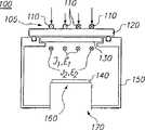
RF電界中の電子を加速するための多数の技法が提案されている。例えば、米国特許第4948458号には、処理すべき半導体ウエハの平面的なに平行に位置する平面的なアンテナ・コイルを使用して、チャンバ内の高周波電界中で電子を励起するプラズマ発生デバイスが開示されている。図1に、アンテナ・システム105、誘電体ウィンドウ120、ガス分配プレート130、処理すべきウエハ140、真空チャンバ150、静電チャック160、および下側電極170を含んでいるプラズマ発生デバイス100を概略的に示す。 A number of techniques have been proposed for accelerating electrons in an RF field. For example, U.S. Pat. No. 4,948,458 discloses a plasma generating device that excites electrons in a high frequency electric field in a chamber using a planar antenna coil positioned in parallel to a planar surface of a semiconductor wafer to be processed. It is disclosed. FIG. 1 schematically illustrates a
動作に際しては、高周波発生源(図示せず)を使用して、一般に高周波整合回路(図示せず)を介して、アンテナ・システム105に高周波電流を供給する。高周波電流は、一般にアンテナ・システム105を介して共振し、真空チャンバ150内で方位角電界を誘導する。同時に、ガス分配プレート130を介してプロセス・ガスを真空チャンバ150中に導入すると、誘導された電界によりプロセス・ガスがイオン化してチャンバ150内にプラズマが生成される。次いでプラズマは、(静電チャック160によって所定の位置に保持された)ウエハ140に当たり、ウエハ140を必要に応じて処理する(例えば、エッチングする)。一般に、アンテナ・コイルに加えられる周波数とは異なる周波数である別の高周波数を下側電極170に加えて、イオン衝撃用の負のDCバイアス電圧を得る。 In operation, a high frequency generator (not shown) is used to supply a high frequency current to the
図2Aおよび図2Bに、米国特許第4948458号に示されているアンテナ・システムを構成する2つの渦巻き状の平面的なコイル110a、110bを示す。図2Aに示すように、第1の平面的なコイル110aは、平面的なスパイラルに形成された一つの導電エレメントとして構成され、高周波回路への接続のために高周波タップ205、215に接続されている。図2Bでは、別の平面的なコイル110bは、相互接続225を介して直列に接続された複数の接続リング220として構成され、各端部が高周波タップ205、215に接続されている。 2A and 2B show two spiral
当技術分野においてよく知られているように、そのような渦巻き状のコイルによって得られる円状電流パターンはドーナツ形プラズマを作り出し、これによりウエハ140におけるエッチング速度に半径方向の不均一性が生じることがある。言い換えれば、平面的なコイル・アンテナ110によって誘導的に発生する電界は、一般に、(半径方向成分Er=0および方位角成分Eθ≠0を有する)方位角電界であるが、中心部では0である(Er=0およびEθ≠0)。したがって、コイル・アンテナ110は、中心部においてより低い密度を有するドーナツ形プラズマを生成するので、ドーナツの中心部において適切な均一性を得るためには、プラズマ拡散(すなわち、中心部への電子およびイオンの拡散)を利用しなければならない。ただし、用途によっては、プラズマ拡散によって得られる均一性は不十分である。 As is well known in the art, the circular current pattern obtained by such a spiral coil creates a donut-shaped plasma, which results in radial non-uniformities in the etch rate on the
さらに、そのような渦巻き状のコイル・アンテナは方位角不均一プラズマをつくる傾向がある。これは、平面的なアンテナ・コイルを構成するために使用される結合線路の比較的長い長さが、コイルが一般に動作する高周波数においてかなりの電気的長さを有することに起因する。電圧波および電流波は入力端部から端子端部まで順方向に進行し、端子端部において再び反射されることになる。順方向波および反射波の重ね合わせの結果、コイルに定在波が生じる(すなわち、電圧および電流がコイルの長さに沿って周期的に変化する)。コイルを端子端部において接地した場合、端子端部における電流は最大値になり、端子端部における電圧は0になる。入力に向かってコイルに沿って進むと、電圧は増大し、電流は減少し、ついには電気的長さが90度のところで、電圧は最大値になり、電流は最小値になる。そのようなある程度の変化があると、極めて不均一なプラズマが生じる。したがって、平面的なコイルは一般にキャパシタンスで終端され、それによりコイル中の電流はコイルの両端部において同じになり、コイルの中央部の近くで最大値まで増大する。そうするとプラズマ均一性を改善することができるが、電流がコイルの長さに沿って方位角方向に変化するので、方位角不均一性はまだ存在する。例えば、図2Aの点Pは電流最大値である。点Pのいずれかの側で、電流は低下する。したがって、プラズマに結合する電力はPの下でより大きくなり、対応するプラズマはより密になる。反対に、点P’におけるプラズマ密度は比較的低くなる。 Furthermore, such spiral coil antennas tend to produce azimuthal non-uniform plasma. This is due to the relatively long length of the coupled line used to construct a planar antenna coil has a significant electrical length at the high frequencies at which the coil generally operates. The voltage wave and current wave travel in the forward direction from the input end to the terminal end and are reflected again at the terminal end. As a result of the superposition of the forward and reflected waves, a standing wave is generated in the coil (ie, voltage and current change periodically along the length of the coil). When the coil is grounded at the terminal end, the current at the terminal end is maximum and the voltage at the terminal end is zero. Proceeding along the coil toward the input, the voltage increases, the current decreases, and finally at the electrical length of 90 degrees, the voltage reaches a maximum value and the current reaches a minimum value. Such a certain amount of change results in a very non-uniform plasma. Thus, a planar coil is generally terminated with a capacitance so that the current in the coil is the same at both ends of the coil and increases to a maximum near the center of the coil. This can improve plasma uniformity, but azimuthal non-uniformity still exists because the current changes in the azimuthal direction along the length of the coil. For example, the point P in FIG. 2A is the maximum current value. On either side of point P, the current drops. Thus, the power coupled to the plasma is greater under P and the corresponding plasma is denser. Conversely, the plasma density at point P 'is relatively low.
終端コンデンサ値は変化させることができるが、そうするとコイルに沿った電圧の位置が変化するだけであることに留意されたい。さらに、コイル長さに沿って同じ極性の電圧を得るためにコイルをインダクタンスで終端させることができるが、コイルの中心位置のどこかに電流ゼロが存在することになり(電流はゼロのいずれかの側で反対方向に流れる)、生じたプラズマ密度は容認できないほど低くかつ不均一になることがある。Patrick他の米国特許第5401350号は上述の欠点を克服しようと試みるものである。そこには、プラズマ均一性を改善するための複数平面的なコイル構成が記載されている。個々のコイルへのRF電力は独立して制御され、電力および位相の独立した調整に対処する別個の電力源および別個の整合回路網が必要となる。 Note that the termination capacitor value can be varied, but that will only change the position of the voltage along the coil. In addition, the coil can be terminated with an inductance to obtain a voltage of the same polarity along the length of the coil, but there will be a zero current somewhere in the center of the coil (the current is either zero) The resulting plasma density may be unacceptably low and non-uniform. Patrick et al. US Pat. No. 5,401,350 attempts to overcome the above-mentioned drawbacks. There, a multi-planar coil configuration for improving plasma uniformity is described. The RF power to the individual coils is controlled independently, requiring a separate power source and a separate matching network to handle independent power and phase adjustments.
プラズマ結合システム内で誘導結合均一性を制御するための改善された方法および装置が必要であることは明らかである。 Clearly, there is a need for an improved method and apparatus for controlling inductive coupling uniformity within a plasma coupling system.
本発明は、アンテナ・システム内の誘導結合均一性を改善するためのシステムを提供することによって、従来技術の上記で特定した欠点を克服するものである。アンテナ・コイルの配置および電流分布を制御することによって、プラズマ均一性を改善することができる。 The present invention overcomes the above-identified shortcomings of the prior art by providing a system for improving inductive coupling uniformity within an antenna system. By controlling antenna coil placement and current distribution, plasma uniformity can be improved.
例示的な実施形態によれば、2つまたはそれ以上の渦巻き状のコイルがプラズマ・チャンバの誘電体ウィンドウ上に配置される。各コイルは平面的なコイルか、または平面的なコイルと垂直方向に積み重なったらせん状のコイルの両方の組合せのいずれかである。各コイルの入力端部は入力側可変コンデンサに取り付けられ、出力端部は出力側可変コンデンサを介して接地に終端される。出力側コンデンサは、電流が極値(すなわち、最大値または最小値)であるかどうか、または電圧が極値であるかどうかを決定し、入力側コンデンサは、各コイルの全インピーダンスを変化させることができ、これらの複数のコイルの電流の大きさの比を変化させることができる。各コイルにおける電流の大きさおよび最大電流の場所を調整することによって、プラズマ密度、すなわち、プラズマ均一性を制御することができる。 According to an exemplary embodiment, two or more spiral coils are placed on the dielectric window of the plasma chamber. Each coil is either a planar coil or a combination of both a planar coil and a spiral coil stacked vertically. The input end of each coil is attached to the input side variable capacitor, and the output end is terminated to the ground via the output side variable capacitor. The output capacitor determines whether the current is extreme (ie, maximum or minimum) or the voltage is extreme, and the input capacitor changes the total impedance of each coil And the ratio of the current magnitudes of the plurality of coils can be changed. By adjusting the magnitude of the current in each coil and the location of the maximum current, the plasma density, ie plasma uniformity, can be controlled.
以下、本発明の上述した内容、その他の特徴、および、利点について、添付図面に示す例示的な実施形態を参照して詳細に説明する。説明する実施形態は一例であり、また、理解を助けるものであり、多数の同等の実施形態が実現されることはいうまでもない。 Hereinafter, the above-described content, other features, and advantages of the present invention will be described in detail with reference to exemplary embodiments shown in the accompanying drawings. It will be appreciated that the described embodiments are examples and aid in understanding, and that many equivalent embodiments may be implemented.
図1に、本発明のアンテナ・システムを組み込むことができるプラズマ発生デバイス100を示す。プラズマ発生デバイス100は、誘電体ウィンドウ120、ガス分配プレート130、ウェハ140、真空チャンバ150、静電チャック160、下側電極170およびアンテナ・システム105を含んでいる。アンテナ・システム105は、RF整合回路網(図示せず)とRF発生器(図示せず)に接続された一組のコイル110を含んでいる。 FIG. 1 shows a
本発明の例示的な実施形態によれば、このアンテナ・システムは、Transformer−Coupled Plasma(TCPTM、ラム リサーチ コーポレーションの登録商標)アンテナ・システムである。図3に、本発明の第1の実施形態によるTCPTMアンテナ・システム300を示す。この実施形態では、TCPTMアンテナ・システム300は2つの単巻コイルを含んでいる。コイル1は中心部の近くに置かれることが好ましく、コイル2は反応器の上部開口の外縁部に向かってより遠くに置かれることが好ましい。高周波(RF)電流が2つの調整コンデンサC1およびC2を介してコイル1および2の一方の端部に同時に供給される。当技術分野においてよく知られているように、RF入力はRF発生源310によって発生され、RF整合回路網320を介してコンデンサC1およびC2に供給される。調整コンデンサC1およびC2は、それぞれ調整すべきコイル1および2の電流I1およびI2の大きさに対処する。コイル1およびコイル2の反対側の端部は結合され、インピーダンスZTを介して接地に終端される。According to an exemplary embodiment of the present invention, the antenna system is a Transformer-Coupled Plasma (TCP™ , a trademark of Lam Research Corporation) antenna system. FIG. 3 shows a TCP™ antenna system 300 according to a first embodiment of the present invention. In this embodiment, the TCP™ antenna system 300 includes two single turn coils.
平面的な単巻コイルによって誘導的に発生した電界は方位角電界(半径方向成分Er=0および方位角成分Eθ≠0)であるが、中心部では0である(Er=0およびEθ≠0)。誘電体ウィンドウ表面の近くでは、プラズマ中の誘導電界および誘導電流(J=σE)はほぼ駆動コイルの鏡像である。平面的なコイル・アンテナは、駆動コイルの半径の2分の1に近い半径をもつドーナツ形プラズマを生成する。2つのコイルを離して置くことによって、これは、2つのコイルの平均半径の2分の1にほぼ等しい半径を有するより漸進的なプラズマ・ドーナツを効果的に発生する。内側コイルからプラズマへの電力結合は内側領域内に局所化され、外側コイルからの電力結合は外側領域内に局所化される。その結果、プラズマ拡散(すなわち、電子およびイオンの拡散)は中心部および他の場所におけるプラズマ密度をより均一にする傾向がある。The electric field generated inductively by the planar single coil is an azimuth electric field (radial component Er = 0 and azimuthal component Eθ ≠ 0), but zero in the center (Er = 0 andEθ ≠ 0). Near the dielectric window surface, the induced electric field and induced current (J = σE) in the plasma are approximately mirror images of the drive coil. A planar coil antenna produces a donut-shaped plasma with a radius close to one half the radius of the drive coil. By placing the two coils apart, this effectively generates a more gradual plasma donut with a radius approximately equal to one-half of the average radius of the two coils. Power coupling from the inner coil to the plasma is localized in the inner region and power coupling from the outer coil is localized in the outer region. As a result, plasma diffusion (ie, electron and ion diffusion) tends to make the plasma density more uniform in the center and elsewhere.
上記のように、2つの単巻コイルに関連する回路(すなわち、コンデンサC1およびC2およびインピーダンスZT)は、コイル1とコイル2における電流の大きさ、すなわちそれぞれI1とI2の比を調整することができる。電流の大きさを調整することによって、反応器の中心部と縁部の間のプラズマ均一性を調整することができる。当業者なら理解できるように、C1およびC2は固定コンデンサでも可変コンデンサでもよい。As noted above, the circuits associated with the two single turn coils (ie, capacitors C1 and C2 and impedance ZT ) are the magnitude of the current in
入力側調整コンデンサC1およびC2は各コイルの入力誘導リアクタンスを部分的に消去する。C1およびC2の値を適切に選択すれば、各脚の入力リアクタンスは同じになり、その結果、共通の発生源から供給されたときのコイル1およびコイル2への入力電流が等しくなる。これらの開始値からC1をより高く、C2をより低く調整すると、コイル1の電流は減少し、コイル2の電流は増大する。方向を逆にすると、反対方向における電流は不平衡になる。調整プロセス中、一方の脚は増大したリアクタンスを有し、他方の脚は減少したリアクタンスを有するので、複合回路の入力インピーダンスは名目上同じままである。The input side adjustment capacitors C1 and C2 partially eliminate the input inductive reactance of each coil. If the values of C1 and C2 are chosen appropriately, the input reactance of each leg will be the same, resulting in equal input currents to
コイル1とコイル2の反対側の端部はインピーダンスZTで終端することができる。ZTは、従来のTCPTMシステムの場合と同様に共通のコンデンサか、あるいは接地への電気的に短絡した接続でもよい。ZTは、接地に終端された別個のコンデンサとすることもできる。各コイルが異なる電気的長さを有する場合、各コイルの入力インピーダンスも異なる。電流最大値が名目上各コイル長さの中心部に現れるように、別個の終端コンデンサを選択することができる。The opposite end of the
2つのコイルが対称的に平衡しているとき、各コイルに流れる電流は名目上同じになる。C1およびC2の値を変化させると、コイル1およびコイル2への不平衡な電流の流れが得られることが当業者なら理解できよう。入力リアクタンスX1およびX2が誘導性であると仮定すると、C2は、例えば、X1>X2という平衡状態から離れて増大すると、I1>I2である。この場合、内側コイル(コイル1)中の電流は、反応器の中心部により強い誘導結合を生じる外側コイルよりも大きくなる。その結果、比較的高いプラズマ密度がコイル1の下の中心領域内に生じる。別の場合では、外側コイル(コイル2)中の電流を内側コイル中の電流よりも大きくなるように調整し、それにより反応器壁の近くのような、内側コイルを覆っている領域におけるよりも低いプラズマ密度を補償することができる。When the two coils are symmetrically balanced, the current flowing through each coil is nominally the same.One skilled in the art will appreciate that changing the values of C1 and C2 will result in an unbalanced current flow to
上述の2つの単巻コイルの使用法を説明のために簡単に示す。上記の一般原則は複巻コイル、複巻システムに同等に適用可能であることが当業者なら理解できよう。さらに、本発明は(図3に示される)二次元コイルの構成に限定されるものではなく、代わりに三次元コイル構成として実現することもできる。例えば、コイルは、ドーム形誘電体ウィンドウに一致するように構成するか、あるいは円筒形誘電体ウィンドウの周りにらせん状に構成することができる。上記の一般原則は、複数の巻きの複数のコイルを有するドーム形、らせん状、または他の三次元の構成を同様に適用可能であることが当業者なら理解できよう。 The use of the two single turn coils described above is briefly shown for illustration. One skilled in the art will appreciate that the above general principles are equally applicable to multi-turn coils and multi-turn systems. Further, the present invention is not limited to a two-dimensional coil configuration (shown in FIG. 3), but can instead be implemented as a three-dimensional coil configuration. For example, the coil can be configured to match a dome-shaped dielectric window, or it can be configured helically around a cylindrical dielectric window. Those skilled in the art will appreciate that the general principles described above are equally applicable to dome, spiral, or other three-dimensional configurations having multiple coils of multiple turns.
図4に、本発明の第2の実施形態によるTCPTMアンテナ・システム400を示す。図4には、2つの調整コンデンサC1〜C4が取付けられた2つの複巻コイル(コイル1およびコイル2)が示されている。図から明らかなように、コイル1は中心部に配置されおり、コイル2は反応器の上部開口の外縁部に向かってより遠くに配置されていることが好ましい。RF入力は、調整コンデンサC1およびC2を介してコイル1および2の第1の端部に同時に供給される。コイル1および2の反対側の端部はそれぞれ調整コンデンサC3およびC4を介して終端される。図3を参照して上述した二重のコイル単巻システムの場合と同様に、2つのコイルはより漸進的なドーナツ形プラズマを効果的に発生する。電流I1およびI2は同じ方向に流れるので、コイルからプラズマへの電力結合は領域全体に広がり、単一の平坦化されたドーナツ形プラズマを生成する。電流が不平衡である場合、ドーナツ形電界は中心部または外側においてより強くなる。FIG. 4 shows a TCP™ antenna system 400 according to a second embodiment of the present invention. 4 shows, two multiple-turn coils two tuning capacitors C1 -C4 is attached (
コイルに沿ってより対称的な電流分布を得るために、各コイルごとに2つのコンデンサが設けられる。例えば、電流最大値(ならびに純抵抗性インピーダンス点)がコイル1の中心部に現れるように、C1をC3と一緒に調整することができる。コイルの中心部からC1に向かって移動すると、リアクタンスは誘導性になり、コイルの中心部からC3に向かって移動すると、リアクタンスは容量性になり、それにより電流は中心部において最大になり、名目上正弦波の形で中心部から離れて減少する。In order to obtain a more symmetrical current distribution along the coils, two capacitors are provided for each coil. For example, C1 can be adjusted together with C3 so that the current maximum (as well as the pure resistive impedance point) appears in the center of
さらに、C3とC4の調整により上述の方位角不均一プラズマを補償することができる。例えば、図4のコイル1の点P1において最大電流が得られるように、C3を調整することができる。その結果、プラズマへの電力結合はP1の下でより大きくなり、対応するプラズマ密度はより高くなる。これは方位角不均一性を生じる傾向がある。ただし、C4を調整すれば、P1に対向する半径方向軸に沿ったコイル2中の場所P2において最大電流を得ることができる。したがって、P2におけるコイル2のより大きい電力結合がコイル1による影響を相殺し、その結果、より方位角的に均一なプラズマが生じる。C3とC4の調整の別法として、コイル1およびコイル2中の電流最大値がそれぞれP1およびP2のところに現れるように、コイル1の方位角位置をコイル2の方位角位置に対して物理的に回転させることができる。Furthermore, the above-mentioned azimuthal non-uniform plasma can be compensated by adjusting C3 and C4 . For example, C3 can be adjusted so that the maximum current is obtained at the
本発明の例示的な実施形態によれば、調整コンデンサC1およびC2は、1回の制御により反対方向に回転するように構成することができる。このようにすると、入力において単一の従来の整合回路網を妨害することなしに、単一の発生器からの1回の制御により電流の不平衡を、ひいてプラズマ不均一性を最適化することができる。同様に、C3とC4を反対方向に調整しても、C1とC2を調整するのと同じ効果が得られる。According to an exemplary embodiment of the present invention, the regulating capacitors C1 and C2 can be configured to rotate in opposite directions with a single control. In this way, a single control from a single generator optimizes current imbalance and thus plasma inhomogeneity without disturbing a single conventional matching network at the input. be able to. Similarly, adjusting C3 and C4 in the opposite direction has the same effect as adjusting C1 and C2 .
コイル中の巻数が変化するにつれて、コイルとプラズマの間の相互結合は、変圧器の一次コイル(すなわち駆動コイル)と二次コイル(すなわちプラズマ)の間の相互結合と同様の形で変化する(Albert J.Lammの、”Observations of Standing Waves on an InductivePlasma Coil Modeled as a Uniform Transmission Line”,J. Vac. Sci. Tech A, 15巻 No.51997年9月/10月 2615頁を参照されたい。)。巻数の増大/減少はプラズマの密度に影響を及ぼす。例えば、巻数が増大すると相互結合係数が減少し、それによりプラズマ密度が低くなる。一方、コイル長さが短縮された場合、コイル長さにわたって統合された全体的なプラズマの発生が減少する。したがって、各コイルの巻数および全長を最適化して、これら2つのファクタをつりあわせることが可能であることが当業者なら理解できよう。 As the number of turns in the coil changes, the mutual coupling between the coil and the plasma changes in a manner similar to the mutual coupling between the primary coil (ie drive coil) and the secondary coil (ie plasma) of the transformer ( See Albert J. Lamm's “Observations of Standing Waves on an Inductive Plasma Coil Modeled as a Uniform Transmission Line”, J. Vac. Sci. Tech A, 15 No. September / October 51997, page 2615. ). The increase / decrease in the number of turns affects the plasma density. For example, as the number of turns increases, the mutual coupling coefficient decreases, thereby reducing the plasma density. On the other hand, if the coil length is shortened, the overall plasma generation integrated over the coil length is reduced. Thus, those skilled in the art will appreciate that these two factors can be balanced by optimizing the number of turns and the overall length of each coil.
入力側調整コンデンサC1およびC2の値を変化させる影響を説明するために、以下の3つの状況、すなわち、C1の値がC2の値よりも大きい最初の状況、C1とC2の値が等しくなるように調整される第2の状況、およびC1の値がC2の値よりも小さい最後の状況について考えてみる。To illustrate the effect of changing the values of the input-side adjustment capacitors C1 and C2 , the following three situations, namely thefirst situation where the value of C1 is greater than the value of C2 , C1 and C2 Consider a second situation where the values of are adjusted to be equal, and the last situation where the value of C1 is less than the value of C2 .
TCPTMコイル・アンテナの複素伝搬定数(k=α+jβ)は、コイル・アンテナの入力および出力における電圧および電流波形測定値から推測することができる(Lammを参照されたい。)。説明のために、α、βおよび実効特性インピーダンスZ0は3つの状況を通して同じであると仮定する。表Iに各コイルのα、β、Z0、電気的長さ、およびC1〜C4の値を示す。The complex propagation constant (k = α + jβ) of the TCP™ coil antenna can be inferred from voltage and current waveform measurements at the coil antenna input and output (see Lamm). For illustration purposes, it is assumed that α, β and effective characteristic impedance Z 0 are the same throughout the three situations. Table I shows α, β, Z0 , electrical length, and values of C1 to C4 for each coil.

表Iにおいて、Zinは各コイルの入力インピーダンスを表す。2つのコイルの全入力インピーダンスは2.1+j10.5Ωであり、これは各コイルのZinの約2分の1である。表IIに、1000Wの入力RF電力および表Iに記載されているパラメータが与えられたときのi番目のコイルのIi、Ii’、ViおよびVi’の大きさおよび位相角を掲載する。表IIにおいて、Iiは、i(i=1、2)番目のコイルの(図4のRF入力により近い)入力端部における電流を表し、Ii’は、i番目のコイルの(図4のC3およびC4により近い)出力端部における電流を表し、ViおよびVi’はそれぞれi番目のコイルの入力端部および出力端部における電圧を表す。In Table I, Zin represents the input impedance of each coil. Total input impedance of the two coils is 2.1 + j10.5Ω, which is about one-half of Zin for each coil. Table II lists the magnitude and phase angle of the i-th coil Ii , Ii ′ , Vi and Vi ′ given the input RF power of 1000 W and the parameters listed in Table I. To do. In Table II, Ii represents the current at the input end (closer to the RF input in FIG. 4) of the i (i = 1, 2) th coil, and Ii ′ represents the i th coil (FIG. 4). It represents the current in the C3 and closer to the C4) output end, Vi and Vi 'denotes the voltage at the input end and an output end of the i th coil, respectively.
表IIから明らかなように、RF電流および電圧は2つのコイルの間で不平衡であるが、各コイル内では平衡である。内側コイルの全インピーダンスは外側コイルの全インピーダンスよりも大きいので、内側コイル(コイル1)の電流と電圧はどちらも外側コイル(コイル2)の電流と電圧よりも34%小さい。各コイルはコイルの中心部の周りに対称的に平衡しており、したがって各コイルの入力電流および電圧の値は大きさが出力値にほとんど等しい。各コイルの中心部から離れると、インピーダンスは、コイルの入力端部に向かって誘導性に支配されるようになり、出力端部に向かって容量性に支配されるようになる。これは、入力電圧と出力電圧の間の位相角の変化から明らかである。 As is apparent from Table II, the RF current and voltage are unbalanced between the two coils, but are balanced within each coil. Since the total impedance of the inner coil is greater than the total impedance of the outer coil, the current and voltage of the inner coil (coil 1) are both 34% smaller than the current and voltage of the outer coil (coil 2). Each coil is symmetrically balanced around the center of the coil, so that the input current and voltage values of each coil are approximately equal in magnitude to the output value. As they move away from the center of each coil, the impedance will be governed inductively toward the input end of the coil and capacitively toward the output end. This is evident from the change in phase angle between the input voltage and the output voltage.
(C1=C2となるように)C1とC2の値を変化させることが電流I1とI2に及ぼす影響を以下の表IIIおよびIVに示す。The effects of changing the values of C1 and C2 on currents I1 and I2 (so that C1 = C2 ) are shown in Tables III and IV below.
2つのコイルの全入力インピーダンスは2.0+j11.4Ωであり、これは各コイルのZinの約2分の1である。表IVに、1000Wの入力RF電力および表IIIに記載されているパラメータが与えられたときのi番目のコイルのIi、Ii’、ViおよびVi’の大きさおよび位相角を掲載する。The total input impedance of the two coils is 2.0 + j11.4Ω, which is about one half of the Zin of each coil. Table IV lists the magnitude and phase angle of the i th coil, Ii , Ii ′ , Vi and Vi ′ given the input RF power of 1000 W and the parameters listed in Table III. To do.
C1=C2およびC3=C4であり、コイル1はコイル2と同等であるので、RF電流および電圧は2つのコイル間ならびに各コイル内で平衡している。Since C1 = C2 and C3 = C4 and
最後の状況は、C1の値がC2の値よりも小さくなるようにC1とC2の値を変化させることの影響を示す。The last situation shows the effect of the value of C1 is to change the values of C1 and C2 so as to be smaller than the value of C2.
2つのコイルの全入力インピーダンスは2.1+j10.5Ωであり、これは各コイルのZinの約2分の1である。表VIに、1000Wの入力RF電力および表IIIに記載されているパラメータが与えられたときのi番目のコイルのIi、Ii’、ViおよびVi’の大きさおよび位相角を掲載する。The total input impedance of the two coils is 2.1 + j10.5Ω, which is about one half of the Zin of each coil. Table VI lists the magnitude and phase angle of the i-th coil Ii , Ii ′ , Vi and Vi ′ given the input RF power of 1000 W and the parameters listed in Table III. To do.
この場合、内側コイル(コイル1)のRF電流と電圧はどちらも外側コイル(コイル2)の電流と電圧よりも51%大きい。 In this case, both the RF current and voltage of the inner coil (coil 1) are 51% greater than the current and voltage of the outer coil (coil 2).
C1とC2を変化させるだけで、他方のコイルの電流および電圧に対してコイルの電流ならびに電圧を実質上調整することができることが、上記の状況から明らかである。It is clear from the above situation that the coil current and voltage can be substantially adjusted relative to the current and voltage of the other coil simply by changing C1 and C2 .
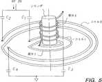
図5に本発明の第3の実施形態を示す。図5では、2つの複巻コイルおよび4つの調整コンデンサC1〜C4の他に、らせん状のコイルが設けられている。この実施形態によれば、内側コイル(コイル1)は2つの部分からなる。部分Iは、図4に関して上述した平面的な複巻コイルを表す。部分IIは、平面的な複巻コイルに対して垂直に置かれ、平面的なコイル(コイル1およびコイル2の部分I)の軸と同一の軸を有するらせん状のコイルを表す。FIG. 5 shows a third embodiment of the present invention. In FIG. 5, a spiral coil is provided in addition to two compound coils and four adjustment capacitors C1 to C4 . According to this embodiment, the inner coil (coil 1) consists of two parts. Part I represents the planar compound coil described above with respect to FIG. Part II represents a helical coil placed perpendicular to the planar compound coil and having the same axis as that of the planar coil (part I of
この実施形態では、内側コイルの電気的長さは、コイル1およびコイル2がそれらの電気的長さに関してより平衡するように延長されている。2つの電気的長さが互いに近接しているとき、各コイルへの電流をより大きい程度まで調整するとともに、より一定の複素入力インピーダンスを維持することができる。本発明によるらせん状のコイルは中心部におけるプラズマへの誘導結合を助ける。らせん状のコイルによって発生される電界も方位角電界であり、中心部において0であるが、この方位角電界の平均半径はらせん状のコイルの直径の程度である。したがって、中心部におけるプラズマをより密にして、よりよい全体的な均一性を得ることができる。 In this embodiment, the electrical length of the inner coil is extended so that
らせん状のコイルの中央部にあるシリンダは誘電体材料でできており、中実にすることにより単に巻線を機械的に支持するが、あるいはその軸に沿って中空にすることもできる。後者の場合、中空シリンダは上端部が真空密封され、また、シリンダの中空領域がチャンバに直接接続されるように底端部が開いている。そのような場合、プロセス・ガスは真空チャンバにだけでなく、中空シリンダにも導入される。シリンダはプラズマ反応器の誘電体ウィンドウの一部と考えることもできる。中空シリンダ中のプラズマ密度は、比較的強い誘導電界および中空陰極効果のためにチャンバ中よりも高くなることがある。中空シリンダ中で生成されるプラズマはチャンバの中心部に拡散する。さらに、一般に10m−トル未満の低圧状況において放電を容易に当てることができるように、比較的高い電圧が終端コンデンサC3によって調整され得る。The cylinder at the center of the helical coil is made of a dielectric material and is solid to simply mechanically support the winding, or it can be hollow along its axis. In the latter case, the hollow cylinder is vacuum sealed at the top and the bottom end is open so that the hollow area of the cylinder is directly connected to the chamber. In such a case, the process gas is introduced not only into the vacuum chamber but also into the hollow cylinder. The cylinder can also be thought of as part of the dielectric window of the plasma reactor. The plasma density in the hollow cylinder may be higher than in the chamber due to the relatively strong induced electric field and the hollow cathode effect. Plasma generated in the hollow cylinder diffuses into the center of the chamber. Moreover, as can be generally 10m- easily shed discharge in a low pressure condition of less than Torr, a relatively high voltage can be adjusted by the termination capacitor C3.
図6に本発明の第4の実施形態を示す。この実施形態によれば、各コイル(コイル1およびコイル2)は2つの部分からなる。部分1は平面的な複巻コイルの形態であり、部分2はらせん状のコイルの形態であって平面的な複巻コイル(すなわち、部分1)に対して直角に置かれ、部分1の軸と同一の軸を有する。 FIG. 6 shows a fourth embodiment of the present invention. According to this embodiment, each coil (
入力高周波はコイル1およびコイル2の平面的な複巻コイルからアンテナ・システム600に入り、また電流が両方のコイル中を同じ方向に流れるように、らせん状のコイルから出る。コイル1およびコイル2の同等の電気的長さを得るために、コイル2のらせん状のコイル(部分2)は平面的な複巻コイル(コイル2の部分1)の最も内側の巻線と同じ半径を有し、コイル1のらせん状のコイル(部分2)は平面的な複巻コイル(コイル1の部分1)の最も外側の巻線と同じ半径を有する。コイル1およびコイル2のらせん状のコイルの巻数は、コイル1およびコイル2の電気的全長がほぼ等しくなるように選択される。コイル1および2のリング間の小さな開口が整列していないことは図6から明らかである。開口が整列している構成とすることは可能であるが、そのような構成にすると、開口の場所におけるプラズマへの電力結合が小さくなることが当業者なら理解できよう。 The input high frequency enters the antenna system 600 from the planar multi-turn coil of
入力調整コンデンサ(C1およびC2)および出力調整コンデンサ(C3およびC4)は図3〜図5に関して上述したものと同様の形でコイル中の電流分布の調整を可能にする。本実施形態は一方のコイル中の電流を独立して調整できること点で有利である。図3〜図5に示した上述の実施形態では、各コイルへの電流は主として、入力インピーダンスを変化させる入力調整コンデンサによって調整される。一方のコイルの入力インピーダンスが変化するにつれて、コイルが電気的に並列に接続されているので、全入力インピーダンスが変化する。これにより一方のコイル中の電流が変化するだけでなく、他方のコイル中の電流も変化することになる。言い換えれば、2つのコイルの電流調整は独立ではない。したがって、全入力インピーダンスのそのような変化を補償するために整合回路網を再同調させなければならない。これは、整合回路網の同調範囲が有限でありかつ制限されているので、すべての用途において実行可能であるとは限らない。Input conditioning capacitors (C1 and C2 ) and output conditioning capacitors (C3 and C4 ) allow for adjustment of the current distribution in the coil in a manner similar to that described above with respect to FIGS. This embodiment is advantageous in that the current in one coil can be adjusted independently. In the above-described embodiment shown in FIGS. 3-5, the current to each coil is primarily regulated by an input conditioning capacitor that changes the input impedance. As the input impedance of one coil changes, the total input impedance changes because the coils are electrically connected in parallel. This not only changes the current in one coil, but also changes the current in the other coil. In other words, the current adjustment of the two coils is not independent. Therefore, the matching network must be retuned to compensate for such changes in total input impedance. This is not feasible in all applications because the tuning network tuning range is finite and limited.
図6において、平面的な複巻コイル(部分1)中の場所か、またはらせん状のコイル(部分2)中の場所に対して出力コンデンサを調整することによって、各コイルの電流最大値の場所を調整することができる。電流最大値が平面的な複巻コイル中のどこかにあるときには、平面的なコイルがプラズマにより近いので、プラズマへの高周波の電力結合は比較的大きい。同様に、電流最大値がらせん状のコイル中のある場所にある場合、らせん状のコイルがプラズマからより離れており、平面的な複巻コイル中で電流が低下するので、プラズマへの電力結合は弱くなる。したがって、出力コンデンサのみの調整では、最大電流の場所とプラズマへの電力結合の大きさが同時に変化することになる。出力コンデンサが調整されるのと同時に、コイルの比較的不変の入力インピーダンスを維持するために、入力コンデンサは反対方向に調整されることになる。このようにして入力および出力コンデンサを調整することにより、電流の大きさは実質上変化しないが、コイル中の電流定在波パターンがシフトし、これによりプラズマへの電力結合が効果的に変化することが当業者なら理解できよう。その結果、プラズマ均一性を制御可能に維持できるようになる。 In FIG. 6, the location of the maximum current of each coil is adjusted by adjusting the output capacitor relative to the location in the planar compound coil (part 1) or in the spiral coil (part 2). Can be adjusted. When the current maximum is somewhere in the planar compound coil, the planar coil is closer to the plasma, so the high frequency power coupling to the plasma is relatively large. Similarly, if the current maximum is somewhere in the spiral coil, the spiral coil is farther away from the plasma and the current is reduced in a planar compound coil, so power coupling to the plasma Becomes weaker. Therefore, adjustment of only the output capacitor changes simultaneously the location of the maximum current and the magnitude of power coupling to the plasma. At the same time as the output capacitor is adjusted, the input capacitor will be adjusted in the opposite direction in order to maintain the relatively unchanged input impedance of the coil. By adjusting the input and output capacitors in this manner, the current magnitude does not change substantially, but the current standing wave pattern in the coil is shifted, thereby effectively changing the power coupling to the plasma. Those skilled in the art will understand. As a result, the plasma uniformity can be maintained in a controllable manner.
図7に本発明の第5の実施形態による二重コイル結合システムを示す。図7の二重のコイル結合システムは平行なアンテナ・エレメントを使用する。2つのコイル(コイル1およびコイル2)は対称的であり、コイルの各ループは半円と平行とのアンテナ・エレメントからなる。RFは各コイル(平行軸により近い)の平行エレメントの中央に同時に供給され、コイルの他の端部は結合され、コンデンサCTを介して接地に終端される。FIG. 7 shows a double coil coupling system according to a fifth embodiment of the present invention. The dual coil coupling system of FIG. 7 uses parallel antenna elements. The two coils (
渦巻き状の平面的なコイルとは対照的に、平面的なアンテナ結合方式は常に比較的大きい電界を中心部において生成し、したがってプラズマ均一性を本質的に改善する(J.J. Chen他、”Parallel-Antenna Transformer-Coupled Plasma GenerationSystem” 米国特許出願第09/052144号、出願日1998年3月31日を参照されたい)。従来のTCPTMコイルと同様に、各コイルによって生成されたプラズマはドーナツ形であり、コイル1ではo1の周り、コイル2ではo2の周りを中心とすることができる。単一のTCPTMと比較して、各プラズマ・ドーナツの半径はかなり短く、それにより従来のTCPTMシステムと比較して、プラズマがドーナツの中心部に拡散しやすくなる。この結合システムの利点は、各コイルの電気的長さがほぼ2分の1になるので、各コイルに沿ったRF電流および電圧の変化がより小さくなることである。In contrast to spiral planar coils, planar antenna coupling always produces a relatively large electric field in the center, thus essentially improving plasma uniformity (JJ Chen et al., “Parallel- Antenna Transformer-Coupled Plasma Generation System ”(see US patent application Ser. No. 09/052144, filing date March 31, 1998). Similar to conventional TCPTM coils, the plasma generated by each coil is donut shaped and can be centered around o1 in coil1 and around o2 in
以上、本発明の原理、好ましい実施形態および動作モードについて説明した。ただし、本発明は上述した特定の実施形態に限定されるものではない。すなわち、上述した実施形態は限定的なものではなく例示的なものであり、当業者であれば、請求の範囲に記載された本発明の範囲から逸脱することなく、それらの実施形態に変更を加えることができることはいうまでもない。 The principles, preferred embodiments and modes of operation of the present invention have been described above. However, the present invention is not limited to the specific embodiments described above. That is, the above-described embodiments are illustrative rather than limiting, and those skilled in the art can make changes to these embodiments without departing from the scope of the present invention described in the claims. It goes without saying that it can be added.
Claims (65)
Translated fromJapaneseチャンバ中に電磁界経路を形成するウィンドウと該チャンバ中にプロセス・ガスを導入するように構成されたプロセス・ガス供給源とを有するプラズマ反応チャンバと、
前記チャンバのウィンドウに近接して配設された少なくとも第1および第2のアンテナ・セグメントを含む高周波アンテナと、前記アンテナ・セグメントに結合され、前記アンテナ・セグメント中の高周波電流を共振させるように構成された高周波発生源と、を備え、
前記高周波電流によって誘導された電磁界は、前記ウィンドウを通過し、プロセス・ガスを励起してイオン化し、それによりチャンバ内にプラズマを発生させ、かつ、
前記第1のアンテナ・セグメントが、前記第2のアンテナ・セグメントを取り囲んでいることを特徴とする装置。An apparatus for generating inductively coupled plasma,
A plasma reaction chamber having a window forming an electromagnetic field path in the chamber and a process gas source configured to introduce process gas into the chamber;
A high frequency antenna including at least first and second antenna segments disposed proximate to the chamber window and coupled to the antenna segment to resonate high frequency current in the antenna segment A high-frequency generation source,
An electromagnetic field induced by the high frequency current passes through the window to excite and ionize a process gas, thereby generating a plasma in the chamber; and
The apparatus wherein the first antenna segment surrounds the second antenna segment.
各々の前記アンテナ・セグメントにより大きい電流を供給し、これにより前記アンテナ・セグメントに隣接するプラズマ領域への高周波電力結合がより大きくなるか、又は、
各々の前記アンテナ・セグメントにより小さい電流を供給し、これにより前記プラズマ領域への電力結合がより小さくなることを特徴とする請求項7に記載の装置。The at least one input side adjustment capacitor comprises:
Providing a larger current to each of the antenna segments, thereby increasing the high frequency power coupling to the plasma region adjacent to the antenna segments, or
8. The apparatus of claim 7, wherein a smaller current is supplied to each of the antenna segments, thereby reducing power coupling to the plasma region.
前記出力側コンデンサは、さらに、電流最大値の場所が方位角的に約180度離れ、かつ半径方向に互いに対向するように前記場所を調整し、それにより方位角不均一電流分布によるプラズマ方位角不均一性を大幅に低減することを特徴とする請求項12に記載の装置。The location of the maximum current in the first and second antenna segments is determined by the rotational position of the first antenna segment relative to the second antenna segment;
The output-side capacitor further adjusts the location so that the location of the maximum current value is azimuthally about 180 degrees apart from each other in the radial direction, thereby causing a plasma azimuth angle due to an azimuthal nonuniform current distribution The apparatus of claim 12, wherein the non-uniformity is significantly reduced.
チャンバ中に電磁界経路を形成するウィンドウと、前記チャンバ中にプロセス・ガスを導入するように構成されたプロセス・ガス供給源とを有するプラズマ反応チャンバと、前記チャンバのウィンドウに近接して配置された少なくとも第1および第2の複巻アンテナ・セグメントを含む高周波アンテナと、
前記アンテナ・セグメントに結合され、前記アンテナ・セグメント中の高周波電流を共振させるように構成された高周波発生源と、を備え、前記高周波電流によって誘導された電磁界は、前記ウィンドウを通過し、プロセス・ガスを励起してイオン化し、それにより前記チャンバ内にプラズマを発生させ、また、
前記第1の複巻アンテナ・セグメントが、前記第2の複巻アンテナ・セグメントを取り囲む外側コイルであることを特徴とする装置。An apparatus for generating inductively coupled plasma,
A plasma reaction chamber having a window forming an electromagnetic field path in the chamber and a process gas source configured to introduce process gas into the chamber; and disposed proximate to the window of the chamber. A high frequency antenna including at least first and second compound antenna segments;
A high frequency source coupled to the antenna segment and configured to resonate high frequency current in the antenna segment, wherein the electromagnetic field induced by the high frequency current passes through the window, and Exciting and ionizing the gas, thereby generating a plasma in the chamber, and
The apparatus wherein the first compound antenna segment is an outer coil surrounding the second compound antenna segment.
各アンテナ・セグメントにより大きい電流を供給し、これにより前記アンテナ・セグメントに隣接するプラズマ領域への高周波電力結合がより大きくなるか、又は、
各アンテナ・セグメントにより小さい電流を供給し、これにより前記プラズマ領域への電力結合がより小さくなることを特徴とする請求項33に記載の装置。The at least one input side adjustment capacitor comprises:
Providing a larger current to each antenna segment, thereby increasing the high frequency power coupling to the plasma region adjacent to the antenna segment, or
34. The apparatus of claim 33, wherein a smaller current is provided to each antenna segment, thereby reducing power coupling to the plasma region.
前記出力側コンデンサは、さらに、電流最大値の場所が方位角的に約180度離れ、かつ半径方向に互いに対向するように前記場所を調整し、それにより方位角不均一電流分布によるプラズマ方位角不均一性を大幅に低減することを特徴とする請求項37に記載の装置。The location of the current maximum in the first and second antenna segments is determined by the rotational position of the first antenna segment relative to the second antenna segment;
The output-side capacitor further adjusts the location so that the location of the maximum current value is azimuthally about 180 degrees apart from each other in the radial direction, thereby causing a plasma azimuth angle due to an azimuthal nonuniform current distribution 38. The apparatus of claim 37, wherein the non-uniformity is significantly reduced.
前記入力側コンデンサの調整の結果、高周波数の全入力インピーダンスが比較的不変に維持され、それにより一方の複巻アンテナ・セグメント中の電流が他方の複巻アンテナ・セグメント中の電流に影響を及ぼさなくなることを特徴とする請求項41に記載の装置。Furthermore, an input side capacitor related to the output side capacitor is included,
As a result of the adjustment of the input-side capacitor, the total input impedance at high frequencies is kept relatively unchanged, so that the current in one multi-turn antenna segment affects the current in the other multi-turn antenna segment. 42. The apparatus of claim 41, wherein the apparatus is eliminated.
前記入力コンデンサの調整の結果、高周波数の全入力インピーダンスが比較的不変に維持され、それにより一方の複巻アンテナ・セグメント中の電流が他方の複巻アンテナ・セグメント中の電流に影響を及ぼさなくなることを特徴とする請求項42に記載の装置。Furthermore, an input side capacitor related to the output side capacitor is included,
As a result of the adjustment of the input capacitor, the total input impedance at high frequencies remains relatively unchanged so that the current in one compound antenna segment does not affect the current in the other compound antenna segment. 43. The apparatus of claim 42.
チャンバ中に電磁界経路を形成するウィンドウと、該チャンバ中にプロセス・ガスを導入するように構成されたプロセス・ガス供給源とを有するプラズマ反応チャンバと、
前記チャンバのウィンドウに近接して配置された同様の形状の2つのアンテナ・セグメントを含む高周波アンテナと、前記アンテナ・セグメントに結合され、前記アンテナ・セグメント中の高周波電流を共振させるように構成された高周波発生源と、を備え、
前記高周波電流によって誘導された電磁界は、前記ウィンドウを通過し、プロセス・ガスを励起してイオン化し、それにより前記チャンバ内にプラズマを発生させ、また、
前記2つのアンテナ・セグメントが離間し、中心軸の周りに対称に配置されていることを特徴とする装置。An apparatus for generating inductively coupled plasma,
A plasma reaction chamber having a window forming an electromagnetic field path in the chamber and a process gas source configured to introduce process gas into the chamber;
A high frequency antenna including two similarly shaped antenna segments disposed proximate to the chamber window and coupled to the antenna segment and configured to resonate high frequency current in the antenna segment A high frequency source,
The electromagnetic field induced by the high frequency current passes through the window and excites and ionizes process gas, thereby generating a plasma in the chamber, and
A device characterized in that the two antenna segments are spaced apart and arranged symmetrically around a central axis.
前記2つのアンテナ・セグメントの出力端部が結合され、かつ、可変コンデンサを介して接地に終端されていることを特徴とする請求項50に記載の装置。The input ends of the two antenna segments are combined, and
51. The apparatus of claim 50, wherein the output ends of the two antenna segments are coupled and terminated to ground through a variable capacitor.
離間した第1および第2の同心電流経路を備え、
前記同心電流経路内の電流が、同じ方向に流れることを特徴とするシステム。An inductively coupled plasma antenna system for a plasma reaction chamber comprising:
Comprising spaced apart first and second concentric current paths;
A system characterized in that currents in the concentric current paths flow in the same direction.
Applications Claiming Priority (2)
| Application Number | Priority Date | Filing Date | Title |
|---|---|---|---|
| US09/106,852 | 1998-06-30 | ||
| US09/106,852US6164241A (en) | 1998-06-30 | 1998-06-30 | Multiple coil antenna for inductively-coupled plasma generation systems |
Related Parent Applications (1)
| Application Number | Title | Priority Date | Filing Date |
|---|---|---|---|
| JP2000557486ADivisionJP5165821B2 (en) | 1998-06-30 | 1999-06-18 | Multi-coil antenna for inductively coupled plasma generation system |
Publications (2)
| Publication Number | Publication Date |
|---|---|
| JP2011146721Atrue JP2011146721A (en) | 2011-07-28 |
| JP5881954B2 JP5881954B2 (en) | 2016-03-09 |
Family
ID=22313609
Family Applications (3)
| Application Number | Title | Priority Date | Filing Date |
|---|---|---|---|
| JP2000557486AExpired - Fee RelatedJP5165821B2 (en) | 1998-06-30 | 1999-06-18 | Multi-coil antenna for inductively coupled plasma generation system |
| JP2009181946AExpired - LifetimeJP4750879B2 (en) | 1998-06-30 | 2009-08-04 | Plasma generator |
| JP2011024421AExpired - Fee RelatedJP5881954B2 (en) | 1998-06-30 | 2011-02-07 | Plasma generator |
Family Applications Before (2)
| Application Number | Title | Priority Date | Filing Date |
|---|---|---|---|
| JP2000557486AExpired - Fee RelatedJP5165821B2 (en) | 1998-06-30 | 1999-06-18 | Multi-coil antenna for inductively coupled plasma generation system |
| JP2009181946AExpired - LifetimeJP4750879B2 (en) | 1998-06-30 | 2009-08-04 | Plasma generator |
Country Status (8)
| Country | Link |
|---|---|
| US (2) | US6164241A (en) |
| EP (1) | EP1092229B1 (en) |
| JP (3) | JP5165821B2 (en) |
| KR (1) | KR100645469B1 (en) |
| AU (1) | AU4954499A (en) |
| DE (1) | DE69939321D1 (en) |
| TW (1) | TW510149B (en) |
| WO (1) | WO2000000993A1 (en) |
Cited By (6)
| Publication number | Priority date | Publication date | Assignee | Title |
|---|---|---|---|---|
| WO2013046495A1 (en)* | 2011-09-30 | 2013-04-04 | パナソニック株式会社 | Atmospheric-pressure-plasma-generating device and method for generating atmospheric-pressure plasma |
| JP2013162034A (en)* | 2012-02-07 | 2013-08-19 | Tokyo Electron Ltd | Inductive coupling plasma processing method, and inductive coupling plasma processing device |
| JP6013666B1 (en)* | 2015-01-16 | 2016-10-25 | 株式会社アルバック | Plasma processing equipment |
| JP2018133232A (en)* | 2017-02-16 | 2018-08-23 | トヨタ紡織株式会社 | Induction heating device and coating drying method |
| WO2019074233A1 (en)* | 2017-10-13 | 2019-04-18 | 주식회사 유진테크 | Icp antenna and plasma treatment device |
| JP2022180536A (en)* | 2017-10-09 | 2022-12-06 | アプライド マテリアルズ インコーポレイテッド | Improvement of inductively coupled plasma source |
Families Citing this family (209)
| Publication number | Priority date | Publication date | Assignee | Title |
|---|---|---|---|---|
| TW389894B (en)* | 1997-06-19 | 2000-05-11 | Optrom Kk | Device for exchanging information with storage medium having electronic circuit and the electronic circuit, and system including the same |
| US7166816B1 (en) | 1997-06-26 | 2007-01-23 | Mks Instruments, Inc. | Inductively-coupled torodial plasma source |
| US6815633B1 (en) | 1997-06-26 | 2004-11-09 | Applied Science & Technology, Inc. | Inductively-coupled toroidal plasma source |
| US7569790B2 (en) | 1997-06-26 | 2009-08-04 | Mks Instruments, Inc. | Method and apparatus for processing metal bearing gases |
| US6150628A (en) | 1997-06-26 | 2000-11-21 | Applied Science And Technology, Inc. | Toroidal low-field reactive gas source |
| US8779322B2 (en) | 1997-06-26 | 2014-07-15 | Mks Instruments Inc. | Method and apparatus for processing metal bearing gases |
| US6924455B1 (en) | 1997-06-26 | 2005-08-02 | Applied Science & Technology, Inc. | Integrated plasma chamber and inductively-coupled toroidal plasma source |
| DE19900179C1 (en)* | 1999-01-07 | 2000-02-24 | Bosch Gmbh Robert | Installation for etching substrates by high-density plasmas comprises a phase delay line causing the supply voltages at both ends of the inductively coupled plasma coil to be in counter-phase with one another |
| US6447635B1 (en)* | 1999-08-24 | 2002-09-10 | Bethel Material Research | Plasma processing system and system using wide area planar antenna |
| KR100338057B1 (en)* | 1999-08-26 | 2002-05-24 | 황 철 주 | Antenna device for generating inductively coupled plasma |
| US6320320B1 (en)* | 1999-11-15 | 2001-11-20 | Lam Research Corporation | Method and apparatus for producing uniform process rates |
| RU2171555C1 (en)* | 2000-03-06 | 2001-07-27 | Берлин Евгений Владимирович | High-frequency gaseous-discharge source of high-density ions with low-impedance antenna |
| US6413359B1 (en)* | 2000-04-04 | 2002-07-02 | K2 Keller Consulting | Plasma reactor with high selectivity and reduced damage |
| US6401652B1 (en)* | 2000-05-04 | 2002-06-11 | Applied Materials, Inc. | Plasma reactor inductive coil antenna with flat surface facing the plasma |
| DE10024883A1 (en)* | 2000-05-19 | 2001-11-29 | Bosch Gmbh Robert | Plasma etching system |
| KR20010112958A (en)* | 2000-06-15 | 2001-12-24 | 황 철 주 | High density plasma reactor |
| JP2002008996A (en)* | 2000-06-23 | 2002-01-11 | Mitsubishi Heavy Ind Ltd | Feed antenna and feed method |
| US6531029B1 (en)* | 2000-06-30 | 2003-03-11 | Lam Research Corporation | Vacuum plasma processor apparatus and method |
| US6685798B1 (en) | 2000-07-06 | 2004-02-03 | Applied Materials, Inc | Plasma reactor having a symmetrical parallel conductor coil antenna |
| US6694915B1 (en) | 2000-07-06 | 2004-02-24 | Applied Materials, Inc | Plasma reactor having a symmetrical parallel conductor coil antenna |
| US6409933B1 (en)* | 2000-07-06 | 2002-06-25 | Applied Materials, Inc. | Plasma reactor having a symmetric parallel conductor coil antenna |
| US6414648B1 (en)* | 2000-07-06 | 2002-07-02 | Applied Materials, Inc. | Plasma reactor having a symmetric parallel conductor coil antenna |
| US6462481B1 (en) | 2000-07-06 | 2002-10-08 | Applied Materials Inc. | Plasma reactor having a symmetric parallel conductor coil antenna |
| US7223676B2 (en) | 2002-06-05 | 2007-05-29 | Applied Materials, Inc. | Very low temperature CVD process with independently variable conformality, stress and composition of the CVD layer |
| US6939434B2 (en) | 2000-08-11 | 2005-09-06 | Applied Materials, Inc. | Externally excited torroidal plasma source with magnetic control of ion distribution |
| US6893907B2 (en) | 2002-06-05 | 2005-05-17 | Applied Materials, Inc. | Fabrication of silicon-on-insulator structure using plasma immersion ion implantation |
| US7166524B2 (en) | 2000-08-11 | 2007-01-23 | Applied Materials, Inc. | Method for ion implanting insulator material to reduce dielectric constant |
| US7294563B2 (en) | 2000-08-10 | 2007-11-13 | Applied Materials, Inc. | Semiconductor on insulator vertical transistor fabrication and doping process |
| US7137354B2 (en) | 2000-08-11 | 2006-11-21 | Applied Materials, Inc. | Plasma immersion ion implantation apparatus including a plasma source having low dissociation and low minimum plasma voltage |
| US7037813B2 (en) | 2000-08-11 | 2006-05-02 | Applied Materials, Inc. | Plasma immersion ion implantation process using a capacitively coupled plasma source having low dissociation and low minimum plasma voltage |
| US7430984B2 (en) | 2000-08-11 | 2008-10-07 | Applied Materials, Inc. | Method to drive spatially separate resonant structure with spatially distinct plasma secondaries using a single generator and switching elements |
| US7288491B2 (en) | 2000-08-11 | 2007-10-30 | Applied Materials, Inc. | Plasma immersion ion implantation process |
| US7303982B2 (en) | 2000-08-11 | 2007-12-04 | Applied Materials, Inc. | Plasma immersion ion implantation process using an inductively coupled plasma source having low dissociation and low minimum plasma voltage |
| US7479456B2 (en) | 2004-08-26 | 2009-01-20 | Applied Materials, Inc. | Gasless high voltage high contact force wafer contact-cooling electrostatic chuck |
| US7094670B2 (en) | 2000-08-11 | 2006-08-22 | Applied Materials, Inc. | Plasma immersion ion implantation process |
| US7320734B2 (en) | 2000-08-11 | 2008-01-22 | Applied Materials, Inc. | Plasma immersion ion implantation system including a plasma source having low dissociation and low minimum plasma voltage |
| US7465478B2 (en) | 2000-08-11 | 2008-12-16 | Applied Materials, Inc. | Plasma immersion ion implantation process |
| US7183177B2 (en) | 2000-08-11 | 2007-02-27 | Applied Materials, Inc. | Silicon-on-insulator wafer transfer method using surface activation plasma immersion ion implantation for wafer-to-wafer adhesion enhancement |
| KR100444189B1 (en)* | 2001-03-19 | 2004-08-18 | 주성엔지니어링(주) | Impedance matching circuit for inductive coupled plasma source |
| US6527912B2 (en)* | 2001-03-30 | 2003-03-04 | Lam Research Corporation | Stacked RF excitation coil for inductive plasma processor |
| US6583572B2 (en)* | 2001-03-30 | 2003-06-24 | Lam Research Corporation | Inductive plasma processor including current sensor for plasma excitation coil |
| US7096819B2 (en)* | 2001-03-30 | 2006-08-29 | Lam Research Corporation | Inductive plasma processor having coil with plural windings and method of controlling plasma density |
| KR100404723B1 (en)* | 2001-04-26 | 2003-11-07 | 주식회사 플라즈마트 | Device for Generating Inductively Coupled Plasma with Lower Aspect Ratio |
| RU2196395C1 (en)* | 2001-05-30 | 2003-01-10 | Александров Андрей Федорович | Plasma reactor and plasma generating device (alternatives) |
| KR100476902B1 (en)* | 2001-07-20 | 2005-03-17 | 주식회사 셈테크놀러지 | The Large-Area Plasma Antenna(LAPA) and The Plasma Source For Making Uniform Plasma |
| KR200253559Y1 (en)* | 2001-07-30 | 2001-11-22 | 주식회사 플라즈마트 | Antenna Structure of Inductively Coupled Plasma Generating Device |
| KR100464808B1 (en)* | 2001-08-28 | 2005-01-05 | 최대규 | Multi inductively coupled plasma inductor |
| US7571697B2 (en)* | 2001-09-14 | 2009-08-11 | Lam Research Corporation | Plasma processor coil |
| KR100478106B1 (en)* | 2001-12-10 | 2005-03-24 | (주)울텍 | Apparatus of high density plasma |
| GB2387969B (en)* | 2002-04-13 | 2005-11-30 | Maurice Clifford Hately | Radio antennas |
| KR100488362B1 (en)* | 2002-05-20 | 2005-05-11 | 주식회사 플라즈마트 | Low-Frequency Type Inductively Coupled Plasma Generating Device |
| JP3820188B2 (en)* | 2002-06-19 | 2006-09-13 | 三菱重工業株式会社 | Plasma processing apparatus and plasma processing method |
| AU2002313941A1 (en)* | 2002-07-26 | 2004-02-16 | Plasmart Co. Ltd. | Inductively coupled plasma generator having lower aspect ratio |
| KR100488360B1 (en)* | 2002-07-29 | 2005-05-11 | 주식회사 플라즈마트 | Antenna Structure of Inductively Coupled Plasma Generating Device for Flat Displayer |
| KR100486712B1 (en)* | 2002-09-04 | 2005-05-03 | 삼성전자주식회사 | Inductively coupled plasma generating apparatus with double layer coil antenna |
| US6773558B2 (en)* | 2002-10-15 | 2004-08-10 | Archimedes Technology Group, Inc. | Fluorine generator |
| KR100486724B1 (en)* | 2002-10-15 | 2005-05-03 | 삼성전자주식회사 | Inductively coupled plasma generating apparatus with serpentine coil antenna |
| TW200420201A (en)* | 2002-12-16 | 2004-10-01 | Japan Science & Tech Agency | Plasma generation device, plasma control method and substrate manufacturing method |
| KR100964398B1 (en)* | 2003-01-03 | 2010-06-17 | 삼성전자주식회사 | Inductively Coupled Antenna and Plasma Processing Equipment Employing the Same |
| EP1480250A1 (en)* | 2003-05-22 | 2004-11-24 | HELYSSEN S.à.r.l. | A high density plasma reactor and RF-antenna therefor |
| WO2004108979A1 (en)* | 2003-06-02 | 2004-12-16 | Shincron Co., Ltd. | Thin film forming device and thin film forming method |
| KR100513163B1 (en)* | 2003-06-18 | 2005-09-08 | 삼성전자주식회사 | Icp antenna and plasma generating apparatus using the same |
| US7573000B2 (en)* | 2003-07-11 | 2009-08-11 | Lincoln Global, Inc. | Power source for plasma device |
| CN1823396B (en)* | 2003-07-11 | 2010-05-12 | Nxp股份有限公司 | Inductive-system and manufacturing method thereof, printed circuit board and tuner |
| KR100551138B1 (en)* | 2003-09-09 | 2006-02-10 | 어댑티브프라즈마테크놀로지 주식회사 | Adaptive Plasma Source for Uniform Plasma Generation |
| US20050205211A1 (en)* | 2004-03-22 | 2005-09-22 | Vikram Singh | Plasma immersion ion implantion apparatus and method |
| US7291360B2 (en) | 2004-03-26 | 2007-11-06 | Applied Materials, Inc. | Chemical vapor deposition plasma process using plural ion shower grids |
| US7244474B2 (en) | 2004-03-26 | 2007-07-17 | Applied Materials, Inc. | Chemical vapor deposition plasma process using an ion shower grid |
| US7695590B2 (en) | 2004-03-26 | 2010-04-13 | Applied Materials, Inc. | Chemical vapor deposition plasma reactor having plural ion shower grids |
| SG136148A1 (en)* | 2004-03-30 | 2007-10-29 | Adaptive Plasma Tech Corp | Plasma source coil and plasma chamber using the same |
| KR100530596B1 (en)* | 2004-03-30 | 2005-11-23 | 어댑티브프라즈마테크놀로지 주식회사 | Plasma apparatus comprising plasma source coil for high process uniformity on wafer |
| US8058156B2 (en) | 2004-07-20 | 2011-11-15 | Applied Materials, Inc. | Plasma immersion ion implantation reactor having multiple ion shower grids |
| US7767561B2 (en) | 2004-07-20 | 2010-08-03 | Applied Materials, Inc. | Plasma immersion ion implantation reactor having an ion shower grid |
| US20070287295A1 (en)* | 2004-09-14 | 2007-12-13 | Kim Nam H | Adaptively Plasma Source And Method Of Processing Semiconductor Wafer Using The Same |
| KR100716720B1 (en)* | 2004-10-13 | 2007-05-09 | 에이피티씨 주식회사 | Non-Circular Plasma Source Coil |
| US7666464B2 (en) | 2004-10-23 | 2010-02-23 | Applied Materials, Inc. | RF measurement feedback control and diagnostics for a plasma immersion ion implantation reactor |
| US20060105114A1 (en)* | 2004-11-16 | 2006-05-18 | White John M | Multi-layer high quality gate dielectric for low-temperature poly-silicon TFTs |
| JP2006221852A (en)* | 2005-02-08 | 2006-08-24 | Canon Anelva Corp | Inductively coupled plasma generator |
| US7428915B2 (en) | 2005-04-26 | 2008-09-30 | Applied Materials, Inc. | O-ringless tandem throttle valve for a plasma reactor chamber |
| US7474273B1 (en) | 2005-04-27 | 2009-01-06 | Imaging Systems Technology | Gas plasma antenna |
| US7109098B1 (en) | 2005-05-17 | 2006-09-19 | Applied Materials, Inc. | Semiconductor junction formation process including low temperature plasma deposition of an optical absorption layer and high speed optical annealing |
| US7422775B2 (en) | 2005-05-17 | 2008-09-09 | Applied Materials, Inc. | Process for low temperature plasma deposition of an optical absorption layer and high speed optical annealing |
| US7312162B2 (en) | 2005-05-17 | 2007-12-25 | Applied Materials, Inc. | Low temperature plasma deposition process for carbon layer deposition |
| US7335611B2 (en) | 2005-08-08 | 2008-02-26 | Applied Materials, Inc. | Copper conductor annealing process employing high speed optical annealing with a low temperature-deposited optical absorber layer |
| US7312148B2 (en) | 2005-08-08 | 2007-12-25 | Applied Materials, Inc. | Copper barrier reflow process employing high speed optical annealing |
| US7323401B2 (en) | 2005-08-08 | 2008-01-29 | Applied Materials, Inc. | Semiconductor substrate process using a low temperature deposited carbon-containing hard mask |
| KR100719804B1 (en)* | 2005-08-08 | 2007-05-18 | 주식회사 아이피에스 | Multi-antenna structure |
| US7429532B2 (en) | 2005-08-08 | 2008-09-30 | Applied Materials, Inc. | Semiconductor substrate process using an optically writable carbon-containing mask |
| KR101094919B1 (en)* | 2005-09-27 | 2011-12-16 | 삼성전자주식회사 | Plasma accelerator |
| US20070080141A1 (en)* | 2005-10-07 | 2007-04-12 | Applied Materials, Inc. | Low-voltage inductively coupled source for plasma processing |
| TWI287318B (en) | 2005-12-07 | 2007-09-21 | Ind Tech Res Inst | Radio frequency identification (RFID) antenna and fabricating method thereof |
| US7719471B1 (en) | 2006-04-27 | 2010-05-18 | Imaging Systems Technology | Plasma-tube antenna |
| JP2007311182A (en)* | 2006-05-18 | 2007-11-29 | Tokyo Electron Ltd | Inductively-coupled plasma processing device, and plasma processing method |
| KR100808862B1 (en)* | 2006-07-24 | 2008-03-03 | 삼성전자주식회사 | Substrate Processing Equipment |
| CN101136279B (en)* | 2006-08-28 | 2010-05-12 | 北京北方微电子基地设备工艺研究中心有限责任公司 | Jigger coupling coil and jigger coupling plasma device |
| US20080118663A1 (en)* | 2006-10-12 | 2008-05-22 | Applied Materials, Inc. | Contamination reducing liner for inductively coupled chamber |
| US20080156264A1 (en) | 2006-12-27 | 2008-07-03 | Novellus Systems, Inc. | Plasma Generator Apparatus |
| US8956500B2 (en) | 2007-04-24 | 2015-02-17 | Applied Materials, Inc. | Methods to eliminate “M-shape” etch rate profile in inductively coupled plasma reactor |
| US7999747B1 (en) | 2007-05-15 | 2011-08-16 | Imaging Systems Technology | Gas plasma microdischarge antenna |
| JP2009147556A (en)* | 2007-12-12 | 2009-07-02 | Sony Corp | Antenna, communication device, and method for manufacturing antenna |
| US9591738B2 (en)* | 2008-04-03 | 2017-03-07 | Novellus Systems, Inc. | Plasma generator systems and methods of forming plasma |
| CN102027811B (en)* | 2008-05-22 | 2015-12-09 | Emd株式会社 | Plasma generating device and plasma processing device |
| CN101640091B (en)* | 2008-07-28 | 2011-06-15 | 北京北方微电子基地设备工艺研究中心有限责任公司 | Inductive coupling coil and plasma processing device adopting same |
| US8916022B1 (en) | 2008-09-12 | 2014-12-23 | Novellus Systems, Inc. | Plasma generator systems and methods of forming plasma |
| JP5399151B2 (en)* | 2008-10-27 | 2014-01-29 | 東京エレクトロン株式会社 | Inductively coupled plasma processing apparatus, plasma processing method, and storage medium |
| US8319436B2 (en)* | 2009-02-02 | 2012-11-27 | Advanced Energy Industries, Inc. | Passive power distribution for multiple electrode inductive plasma source |
| JP5231308B2 (en)* | 2009-03-31 | 2013-07-10 | 東京エレクトロン株式会社 | Plasma processing equipment |
| CN101887836B (en)* | 2009-05-14 | 2013-10-30 | 北京北方微电子基地设备工艺研究中心有限责任公司 | Method and device for regulating current distribution and plasma process equipment |
| JP5851681B2 (en)* | 2009-10-27 | 2016-02-03 | 東京エレクトロン株式会社 | Plasma processing equipment |
| CN102056395B (en)* | 2009-10-27 | 2014-05-07 | 东京毅力科创株式会社 | Plasma processing apparatus and plasma processing method |
| US8741097B2 (en) | 2009-10-27 | 2014-06-03 | Tokyo Electron Limited | Plasma processing apparatus and plasma processing method |
| JP5592098B2 (en) | 2009-10-27 | 2014-09-17 | 東京エレクトロン株式会社 | Plasma processing apparatus and plasma processing method |
| PL2502255T3 (en)* | 2009-11-20 | 2014-09-30 | Oerlikon Trading Ag | Coil section assembly for simulating circular coils for vacuum devices |
| KR20120004040A (en)* | 2010-07-06 | 2012-01-12 | 삼성전자주식회사 | Plasma generator |
| JP5916044B2 (en) | 2010-09-28 | 2016-05-11 | 東京エレクトロン株式会社 | Plasma processing apparatus and plasma processing method |
| JP5851682B2 (en)* | 2010-09-28 | 2016-02-03 | 東京エレクトロン株式会社 | Plasma processing equipment |
| US8920599B2 (en)* | 2010-10-19 | 2014-12-30 | Applied Materials, Inc. | High efficiency gas dissociation in inductively coupled plasma reactor with improved uniformity |
| JP5800532B2 (en) | 2011-03-03 | 2015-10-28 | 東京エレクトロン株式会社 | Plasma processing apparatus and plasma processing method |
| JP5800547B2 (en) | 2011-03-29 | 2015-10-28 | 東京エレクトロン株式会社 | Plasma processing apparatus and plasma processing method |
| JP5781349B2 (en) | 2011-03-30 | 2015-09-24 | 東京エレクトロン株式会社 | Plasma processing equipment |
| US9966236B2 (en) | 2011-06-15 | 2018-05-08 | Lam Research Corporation | Powered grid for plasma chamber |
| EP2739984B1 (en)* | 2011-08-01 | 2019-05-01 | Max-Planck-Gesellschaft zur Förderung der Wissenschaften e.V. | An rf coil assembly for mri with a plurality of coil elements distributed over at least two coil rows |
| CN102395243A (en)* | 2011-10-19 | 2012-03-28 | 中微半导体设备(上海)有限公司 | Inductance coupling plasma device for improving uniformity and efficiency of plasmon |
| US9082591B2 (en) | 2012-04-24 | 2015-07-14 | Applied Materials, Inc. | Three-coil inductively coupled plasma source with individually controlled coil currents from a single RF power generator |
| US9111722B2 (en) | 2012-04-24 | 2015-08-18 | Applied Materials, Inc. | Three-coil inductively coupled plasma source with individually controlled coil currents from a single RF power generator |
| RU2503079C1 (en)* | 2012-04-24 | 2013-12-27 | Евгений Владимирович Берлин | Plasma generator (versions) |
| US9685297B2 (en) | 2012-08-28 | 2017-06-20 | Advanced Energy Industries, Inc. | Systems and methods for monitoring faults, anomalies, and other characteristics of a switched mode ion energy distribution system |
| KR20140089458A (en)* | 2013-01-04 | 2014-07-15 | 피에스케이 주식회사 | Plasma chamber and apparatus for treating substrate |
| AU2014232725B2 (en)* | 2013-03-15 | 2018-04-05 | Starfire Industries Llc | Compact high-voltage plasma source for neutron generation |
| US10132884B2 (en)* | 2013-11-15 | 2018-11-20 | New York University | Circular dipole and surface coil loop structures and methods for using the same |
| KR101522891B1 (en) | 2014-04-29 | 2015-05-27 | 세메스 주식회사 | Plasma generating device and apparatus for treating substrate comprising the same |
| US9659751B2 (en) | 2014-07-25 | 2017-05-23 | Applied Materials, Inc. | System and method for selective coil excitation in inductively coupled plasma processing reactors |
| KR101570171B1 (en)* | 2014-07-25 | 2015-11-20 | 세메스 주식회사 | Plasma generating device and apparatus for treating substrate comprising the same |
| CN105590823B (en)* | 2014-10-22 | 2019-07-05 | 上海凯世通半导体股份有限公司 | RF ion source device |
| JP6539986B2 (en) | 2014-11-05 | 2019-07-10 | 東京エレクトロン株式会社 | PLASMA PROCESSING APPARATUS AND PLASMA PROCESSING METHOD |
| JP6582391B2 (en)* | 2014-11-05 | 2019-10-02 | 東京エレクトロン株式会社 | Plasma processing equipment |
| DE102015003379A1 (en)* | 2015-03-17 | 2016-09-22 | Manz Ag | Plasma generating device with an induction coil |
| KR101753620B1 (en)* | 2015-03-19 | 2017-07-19 | 맷슨 테크놀로지, 인크. | Controlling azimuthal uniformity of etch process in plasma processing chamber |
| US9577349B2 (en)* | 2015-06-29 | 2017-02-21 | Near Field Magnetics, Inc. | Near-field magnetic communication antenna |
| JP6053881B2 (en)* | 2015-07-15 | 2016-12-27 | 東京エレクトロン株式会社 | Plasma processing equipment |
| US10187966B2 (en)* | 2015-07-24 | 2019-01-22 | Applied Materials, Inc. | Method and apparatus for gas abatement |
| WO2017104454A1 (en)* | 2015-12-14 | 2017-06-22 | 株式会社村田製作所 | High frequency module and transmission module |
| US10431425B2 (en)* | 2016-02-23 | 2019-10-01 | Tokyo Electron Limited | Poly-phased inductively coupled plasma source |
| CN107134401A (en)* | 2016-02-26 | 2017-09-05 | 中微半导体设备(上海)有限公司 | A kind of control method, RF power divider and ICP equipment |
| CN107134625A (en)* | 2016-02-26 | 2017-09-05 | 中微半导体设备(上海)有限公司 | A kind of control method, RF power divider and ICP equipment |
| CN107134400B (en)* | 2016-02-26 | 2019-02-22 | 中微半导体设备(上海)有限公司 | A kind of control method, RF power divider and ICP equipment |
| JP6675260B2 (en)* | 2016-04-27 | 2020-04-01 | 東京エレクトロン株式会社 | Transformer, plasma processing apparatus, and plasma processing method |
| CN107333378B (en)* | 2016-04-29 | 2019-05-03 | 中微半导体设备(上海)股份有限公司 | A kind of device for inductively coupled plasma processing and its control method |
| KR101798384B1 (en)* | 2016-05-03 | 2017-11-17 | (주)브이앤아이솔루션 | RF antenna structure for inductively coupled plasma processing apparatus |
| US10998124B2 (en)* | 2016-05-06 | 2021-05-04 | Vishay Dale Electronics, Llc | Nested flat wound coils forming windings for transformers and inductors |
| US10896806B2 (en)* | 2016-11-03 | 2021-01-19 | En2Core Technology, Inc. | Inductive coil structure and inductively coupled plasma generation system |
| US10541114B2 (en)* | 2016-11-03 | 2020-01-21 | En2Core Technology, Inc. | Inductive coil structure and inductively coupled plasma generation system |
| KR101826883B1 (en)* | 2016-11-03 | 2018-02-08 | 인투코어테크놀로지 주식회사 | Inductive Coil Structure And Inductively Coupled Plasma Apparatus |
| US10903046B2 (en)* | 2016-11-03 | 2021-01-26 | En2Core Technology, Inc. | Inductive coil structure and inductively coupled plasma generation system |
| KR102015381B1 (en) | 2017-03-29 | 2019-08-29 | 세메스 주식회사 | Plasma generating device and apparatus for treating substrate comprising the same |
| US11424104B2 (en) | 2017-04-24 | 2022-08-23 | Applied Materials, Inc. | Plasma reactor with electrode filaments extending from ceiling |
| US11114284B2 (en)* | 2017-06-22 | 2021-09-07 | Applied Materials, Inc. | Plasma reactor with electrode array in ceiling |
| US10510515B2 (en) | 2017-06-22 | 2019-12-17 | Applied Materials, Inc. | Processing tool with electrically switched electrode assembly |
| US11355321B2 (en) | 2017-06-22 | 2022-06-07 | Applied Materials, Inc. | Plasma reactor with electrode assembly for moving substrate |
| US11651939B2 (en) | 2017-07-07 | 2023-05-16 | Advanced Energy Industries, Inc. | Inter-period control system for plasma power delivery system and method of operating same |
| US11615943B2 (en) | 2017-07-07 | 2023-03-28 | Advanced Energy Industries, Inc. | Inter-period control for passive power distribution of multiple electrode inductive plasma source |
| KR101986744B1 (en)* | 2017-09-27 | 2019-06-07 | 주식회사 유진테크 | Plasma processing apparatus and method |
| US12230476B2 (en) | 2017-11-17 | 2025-02-18 | Advanced Energy Industries, Inc. | Integrated control of a plasma processing system |
| KR20250026880A (en) | 2017-11-17 | 2025-02-25 | 에이이에스 글로벌 홀딩스 피티이 리미티드 | Spatial and temporal control of ion bias voltage for plasma processing |
| US11437221B2 (en) | 2017-11-17 | 2022-09-06 | Advanced Energy Industries, Inc. | Spatial monitoring and control of plasma processing environments |
| US12288673B2 (en) | 2017-11-29 | 2025-04-29 | COMET Technologies USA, Inc. | Retuning for impedance matching network control |
| US11290080B2 (en) | 2017-11-29 | 2022-03-29 | COMET Technologies USA, Inc. | Retuning for impedance matching network control |
| KR101914902B1 (en) | 2018-02-14 | 2019-01-14 | 성균관대학교산학협력단 | Apparatus for generating plasma and apparatus for treating substrate having the same |
| JP7001958B2 (en)* | 2018-03-06 | 2022-01-20 | 日新電機株式会社 | Plasma processing equipment |
| US10636360B2 (en) | 2018-07-10 | 2020-04-28 | A.U. Vista, Inc. | Wireless display panel with multi-channel data transmission and display device using the same |
| KR102435254B1 (en)* | 2018-10-30 | 2022-08-23 | 베이징 나우라 마이크로일렉트로닉스 이큅먼트 씨오., 엘티디. | Induction coil set and reaction chamber |
| KR102081686B1 (en)* | 2019-05-16 | 2020-02-26 | 주식회사 유진테크 | Substrate processing method using plasma |
| US11527385B2 (en) | 2021-04-29 | 2022-12-13 | COMET Technologies USA, Inc. | Systems and methods for calibrating capacitors of matching networks |
| US11114279B2 (en) | 2019-06-28 | 2021-09-07 | COMET Technologies USA, Inc. | Arc suppression device for plasma processing equipment |
| US11596309B2 (en) | 2019-07-09 | 2023-03-07 | COMET Technologies USA, Inc. | Hybrid matching network topology |
| US11107661B2 (en) | 2019-07-09 | 2021-08-31 | COMET Technologies USA, Inc. | Hybrid matching network topology |
| US20210020405A1 (en)* | 2019-07-18 | 2021-01-21 | Tokyo Electron Limited | Equipment and methods for plasma processing |
| EP4022656A4 (en) | 2019-08-28 | 2023-10-04 | Comet Technologies USA, Inc | HIGH POWER LOW FREQUENCY COILS |
| TWI714366B (en)* | 2019-11-26 | 2020-12-21 | 聚昌科技股份有限公司 | Etching machine structure with the vertical position dynamically adjustable of the coil |
| US11887820B2 (en) | 2020-01-10 | 2024-01-30 | COMET Technologies USA, Inc. | Sector shunts for plasma-based wafer processing systems |
| US11521832B2 (en) | 2020-01-10 | 2022-12-06 | COMET Technologies USA, Inc. | Uniformity control for radio frequency plasma processing systems |
| US12027351B2 (en) | 2020-01-10 | 2024-07-02 | COMET Technologies USA, Inc. | Plasma non-uniformity detection |
| US11830708B2 (en) | 2020-01-10 | 2023-11-28 | COMET Technologies USA, Inc. | Inductive broad-band sensors for electromagnetic waves |
| US11670488B2 (en) | 2020-01-10 | 2023-06-06 | COMET Technologies USA, Inc. | Fast arc detecting match network |
| US11605527B2 (en) | 2020-01-20 | 2023-03-14 | COMET Technologies USA, Inc. | Pulsing control match network |
| US11961711B2 (en) | 2020-01-20 | 2024-04-16 | COMET Technologies USA, Inc. | Radio frequency match network and generator |
| CN111769062B (en)* | 2020-07-27 | 2025-09-19 | 上海邦芯半导体科技有限公司 | Inductive coupling reactor and working method thereof |
| JP7547861B2 (en)* | 2020-08-24 | 2024-09-10 | セイコーエプソン株式会社 | Liquid ejection device and drying device |
| US11373844B2 (en) | 2020-09-28 | 2022-06-28 | COMET Technologies USA, Inc. | Systems and methods for repetitive tuning of matching networks |
| KR20220045895A (en)* | 2020-10-06 | 2022-04-13 | 도쿄엘렉트론가부시키가이샤 | Plasma processing apparatus and plasma processing coil |
| KR20220107521A (en)* | 2021-01-25 | 2022-08-02 | (주) 엔피홀딩스 | Reactor, process processing apparatus including the same and method for manufacturing reactor |
| US12057296B2 (en) | 2021-02-22 | 2024-08-06 | COMET Technologies USA, Inc. | Electromagnetic field sensing device |
| KR102323580B1 (en)* | 2021-04-01 | 2021-11-09 | 피에스케이 주식회사 | Plasma generation unit and substrate processing apparatus |
| US11923175B2 (en) | 2021-07-28 | 2024-03-05 | COMET Technologies USA, Inc. | Systems and methods for variable gain tuning of matching networks |
| KR20230037315A (en)* | 2021-09-09 | 2023-03-16 | 삼성전자주식회사 | Electronic device including antenna structure disposed on supporting member |
| KR20230056214A (en)* | 2021-10-20 | 2023-04-27 | 세메스 주식회사 | Plasma processing apparatus and plasma processing method using the same |
| US12046448B2 (en) | 2022-01-26 | 2024-07-23 | Advanced Energy Industries, Inc. | Active switch on time control for bias supply |
| US11942309B2 (en) | 2022-01-26 | 2024-03-26 | Advanced Energy Industries, Inc. | Bias supply with resonant switching |
| US11670487B1 (en) | 2022-01-26 | 2023-06-06 | Advanced Energy Industries, Inc. | Bias supply control and data processing |
| US12243717B2 (en) | 2022-04-04 | 2025-03-04 | COMET Technologies USA, Inc. | Variable reactance device having isolated gate drive power supplies |
| US11657980B1 (en) | 2022-05-09 | 2023-05-23 | COMET Technologies USA, Inc. | Dielectric fluid variable capacitor |
| US12040139B2 (en) | 2022-05-09 | 2024-07-16 | COMET Technologies USA, Inc. | Variable capacitor with linear impedance and high voltage breakdown |
| US12051549B2 (en) | 2022-08-02 | 2024-07-30 | COMET Technologies USA, Inc. | Coaxial variable capacitor |
| US11978613B2 (en) | 2022-09-01 | 2024-05-07 | Advanced Energy Industries, Inc. | Transition control in a bias supply |
| US12132435B2 (en) | 2022-10-27 | 2024-10-29 | COMET Technologies USA, Inc. | Method for repeatable stepper motor homing |
| US12074390B2 (en) | 2022-11-11 | 2024-08-27 | Tokyo Electron Limited | Parallel resonance antenna for radial plasma control |
| KR102844223B1 (en)* | 2022-12-15 | 2025-08-08 | 세메스 주식회사 | Substrate processing apparatus and plasma density control method |
| US20240213005A1 (en)* | 2022-12-23 | 2024-06-27 | Tokyo Electron Limited | System and Method for Plasma Processing |
| US12284747B2 (en) | 2023-03-07 | 2025-04-22 | Finesse Technology Co., Ltd. | Hollow cathode discharge assistant transformer coupled plasma source and operation method of the same |
Citations (6)
| Publication number | Priority date | Publication date | Assignee | Title |
|---|---|---|---|---|
| JPH06267903A (en)* | 1993-01-12 | 1994-09-22 | Tokyo Electron Ltd | Plasma device |
| JPH0850998A (en)* | 1994-08-04 | 1996-02-20 | Kokusai Electric Co Ltd | Plasma processing device |
| JPH0878191A (en)* | 1994-09-06 | 1996-03-22 | Kobe Steel Ltd | Plasma treatment method and device therefor |
| WO1998001893A1 (en)* | 1996-07-10 | 1998-01-15 | Cvc Products, Inc. | Apparatus and method for multi-zone high-density inductively-coupled plasma generation |
| JPH10125497A (en)* | 1996-06-10 | 1998-05-15 | Lam Res Corp | Inductive coupling source for inducing almost uniform plasma flux |
| JPH10154599A (en)* | 1996-10-21 | 1998-06-09 | Applied Materials Inc | Thermal control device for RF plasma reactor |
Family Cites Families (32)
| Publication number | Priority date | Publication date | Assignee | Title |
|---|---|---|---|---|
| US4948458A (en)* | 1989-08-14 | 1990-08-14 | Lam Research Corporation | Method and apparatus for producing magnetically-coupled planar plasma |
| JPH04362091A (en)* | 1991-06-05 | 1992-12-15 | Mitsubishi Heavy Ind Ltd | Plasma chemical vapor deposition apparatus |
| US5392018A (en)* | 1991-06-27 | 1995-02-21 | Applied Materials, Inc. | Electronically tuned matching networks using adjustable inductance elements and resonant tank circuits |
| US6077384A (en)* | 1994-08-11 | 2000-06-20 | Applied Materials, Inc. | Plasma reactor having an inductive antenna coupling power through a parallel plate electrode |
| US5280154A (en)* | 1992-01-30 | 1994-01-18 | International Business Machines Corporation | Radio frequency induction plasma processing system utilizing a uniform field coil |
| US5231334A (en)* | 1992-04-15 | 1993-07-27 | Texas Instruments Incorporated | Plasma source and method of manufacturing |
| US5241245A (en)* | 1992-05-06 | 1993-08-31 | International Business Machines Corporation | Optimized helical resonator for plasma processing |
| US5277751A (en)* | 1992-06-18 | 1994-01-11 | Ogle John S | Method and apparatus for producing low pressure planar plasma using a coil with its axis parallel to the surface of a coupling window |
| JPH06177058A (en)* | 1992-12-10 | 1994-06-24 | Kokusai Electric Co Ltd | Plasma generator |
| US5433812A (en)* | 1993-01-19 | 1995-07-18 | International Business Machines Corporation | Apparatus for enhanced inductive coupling to plasmas with reduced sputter contamination |
| US5401350A (en)* | 1993-03-08 | 1995-03-28 | Lsi Logic Corporation | Coil configurations for improved uniformity in inductively coupled plasma systems |
| KR100264445B1 (en)* | 1993-10-04 | 2000-11-01 | 히가시 데쓰로 | Plasma Treatment Equipment |
| GB9321489D0 (en)* | 1993-10-19 | 1993-12-08 | Central Research Lab Ltd | Plasma processing |
| JP3150027B2 (en)* | 1993-12-17 | 2001-03-26 | 東京エレクトロン株式会社 | Plasma generator and plasma processing apparatus using this plasma generator |
| US5525159A (en)* | 1993-12-17 | 1996-06-11 | Tokyo Electron Limited | Plasma process apparatus |
| US5522934A (en)* | 1994-04-26 | 1996-06-04 | Tokyo Electron Limited | Plasma processing apparatus using vertical gas inlets one on top of another |
| US5587038A (en)* | 1994-06-16 | 1996-12-24 | Princeton University | Apparatus and process for producing high density axially extending plasmas |
| US5580385A (en)* | 1994-06-30 | 1996-12-03 | Texas Instruments, Incorporated | Structure and method for incorporating an inductively coupled plasma source in a plasma processing chamber |
| JP3105403B2 (en)* | 1994-09-14 | 2000-10-30 | 松下電器産業株式会社 | Plasma processing equipment |
| JP2770753B2 (en)* | 1994-09-16 | 1998-07-02 | 日本電気株式会社 | Plasma processing apparatus and plasma processing method |
| US5919382A (en)* | 1994-10-31 | 1999-07-06 | Applied Materials, Inc. | Automatic frequency tuning of an RF power source of an inductively coupled plasma reactor |
| JP3318638B2 (en)* | 1994-11-17 | 2002-08-26 | ソニー株式会社 | Plasma etching / CVD equipment |
| US5589737A (en)* | 1994-12-06 | 1996-12-31 | Lam Research Corporation | Plasma processor for large workpieces |
| JP3104117B2 (en)* | 1995-01-13 | 2000-10-30 | 松下電器産業株式会社 | Plasma processing apparatus and method |
| US5888413A (en)* | 1995-06-06 | 1999-03-30 | Matsushita Electric Industrial Co., Ltd. | Plasma processing method and apparatus |
| US5716451A (en)* | 1995-08-17 | 1998-02-10 | Tokyo Electron Limited | Plasma processing apparatus |
| US6054013A (en)* | 1996-02-02 | 2000-04-25 | Applied Materials, Inc. | Parallel plate electrode plasma reactor having an inductive antenna and adjustable radial distribution of plasma ion density |
| JP3208079B2 (en)* | 1996-02-27 | 2001-09-10 | 松下電器産業株式会社 | High frequency power application device and plasma processing device |
| US6353206B1 (en)* | 1996-05-30 | 2002-03-05 | Applied Materials, Inc. | Plasma system with a balanced source |
| US5800619A (en)* | 1996-06-10 | 1998-09-01 | Lam Research Corporation | Vacuum plasma processor having coil with minimum magnetic field in its center |
| JPH10172792A (en)* | 1996-12-05 | 1998-06-26 | Tokyo Electron Ltd | Plasma processing device |
| US6028395A (en)* | 1997-09-16 | 2000-02-22 | Lam Research Corporation | Vacuum plasma processor having coil with added conducting segments to its peripheral part |
- 1998
- 1998-06-30USUS09/106,852patent/US6164241A/ennot_activeExpired - Lifetime
- 1999
- 1999-06-18JPJP2000557486Apatent/JP5165821B2/ennot_activeExpired - Fee Related
- 1999-06-18WOPCT/US1999/012808patent/WO2000000993A1/enactiveIP Right Grant
- 1999-06-18DEDE69939321Tpatent/DE69939321D1/ennot_activeExpired - Lifetime
- 1999-06-18KRKR1020007015009Apatent/KR100645469B1/ennot_activeExpired - Lifetime
- 1999-06-18AUAU49544/99Apatent/AU4954499A/ennot_activeAbandoned
- 1999-06-18EPEP99933499Apatent/EP1092229B1/ennot_activeExpired - Lifetime
- 1999-06-28TWTW088110874Apatent/TW510149B/ennot_activeIP Right Cessation
- 2000
- 2000-11-15USUS09/711,935patent/US6463875B1/ennot_activeExpired - Lifetime
- 2009
- 2009-08-04JPJP2009181946Apatent/JP4750879B2/ennot_activeExpired - Lifetime
- 2011
- 2011-02-07JPJP2011024421Apatent/JP5881954B2/ennot_activeExpired - Fee Related
Patent Citations (6)
| Publication number | Priority date | Publication date | Assignee | Title |
|---|---|---|---|---|
| JPH06267903A (en)* | 1993-01-12 | 1994-09-22 | Tokyo Electron Ltd | Plasma device |
| JPH0850998A (en)* | 1994-08-04 | 1996-02-20 | Kokusai Electric Co Ltd | Plasma processing device |
| JPH0878191A (en)* | 1994-09-06 | 1996-03-22 | Kobe Steel Ltd | Plasma treatment method and device therefor |
| JPH10125497A (en)* | 1996-06-10 | 1998-05-15 | Lam Res Corp | Inductive coupling source for inducing almost uniform plasma flux |
| WO1998001893A1 (en)* | 1996-07-10 | 1998-01-15 | Cvc Products, Inc. | Apparatus and method for multi-zone high-density inductively-coupled plasma generation |
| JPH10154599A (en)* | 1996-10-21 | 1998-06-09 | Applied Materials Inc | Thermal control device for RF plasma reactor |
Cited By (12)
| Publication number | Priority date | Publication date | Assignee | Title |
|---|---|---|---|---|
| WO2013046495A1 (en)* | 2011-09-30 | 2013-04-04 | パナソニック株式会社 | Atmospheric-pressure-plasma-generating device and method for generating atmospheric-pressure plasma |
| JP2013162034A (en)* | 2012-02-07 | 2013-08-19 | Tokyo Electron Ltd | Inductive coupling plasma processing method, and inductive coupling plasma processing device |
| JP6013666B1 (en)* | 2015-01-16 | 2016-10-25 | 株式会社アルバック | Plasma processing equipment |
| US10079133B2 (en) | 2015-01-16 | 2018-09-18 | Ulvac, Inc. | Plasma processing device |
| JP2018133232A (en)* | 2017-02-16 | 2018-08-23 | トヨタ紡織株式会社 | Induction heating device and coating drying method |
| JP2022180536A (en)* | 2017-10-09 | 2022-12-06 | アプライド マテリアルズ インコーポレイテッド | Improvement of inductively coupled plasma source |
| JP7431296B2 (en) | 2017-10-09 | 2024-02-14 | アプライド マテリアルズ インコーポレイテッド | Improvements in inductively coupled plasma sources |
| US12217938B2 (en) | 2017-10-09 | 2025-02-04 | Applied Materials, Inc. | To an inductively coupled plasma source |
| WO2019074233A1 (en)* | 2017-10-13 | 2019-04-18 | 주식회사 유진테크 | Icp antenna and plasma treatment device |
| KR20190041607A (en)* | 2017-10-13 | 2019-04-23 | 주식회사 유진테크 | Plasma processing apparatus |
| KR101972783B1 (en)* | 2017-10-13 | 2019-08-16 | 주식회사 유진테크 | Icp antenna and plasma processing apparatus including the same |
| JP2020535625A (en)* | 2017-10-13 | 2020-12-03 | ユ−ジーン テクノロジー カンパニー.リミテッド | ICP antenna and plasma device |
Also Published As
| Publication number | Publication date |
|---|---|
| US6463875B1 (en) | 2002-10-15 |
| KR100645469B1 (en) | 2006-11-13 |
| JP2010003699A (en) | 2010-01-07 |
| JP2002519861A (en) | 2002-07-02 |
| DE69939321D1 (en) | 2008-09-25 |
| EP1092229A1 (en) | 2001-04-18 |
| US6164241A (en) | 2000-12-26 |
| KR20010053288A (en) | 2001-06-25 |
| JP5881954B2 (en) | 2016-03-09 |
| JP5165821B2 (en) | 2013-03-21 |
| TW510149B (en) | 2002-11-11 |
| AU4954499A (en) | 2000-01-17 |
| JP4750879B2 (en) | 2011-08-17 |
| WO2000000993A1 (en) | 2000-01-06 |
| EP1092229B1 (en) | 2008-08-13 |
Similar Documents
| Publication | Publication Date | Title |
|---|---|---|
| JP4750879B2 (en) | Plasma generator | |
| US6685798B1 (en) | Plasma reactor having a symmetrical parallel conductor coil antenna | |
| US6414648B1 (en) | Plasma reactor having a symmetric parallel conductor coil antenna | |
| US6462481B1 (en) | Plasma reactor having a symmetric parallel conductor coil antenna | |
| US6694915B1 (en) | Plasma reactor having a symmetrical parallel conductor coil antenna | |
| CN102054648B (en) | Dual mode inductively coupled plasma reactor with adjustable phase coil assembly | |
| US5874704A (en) | Low inductance large area coil for an inductively coupled plasma source | |
| US6288493B1 (en) | Antenna device for generating inductively coupled plasma | |
| US6409933B1 (en) | Plasma reactor having a symmetric parallel conductor coil antenna | |
| JP5907652B2 (en) | Plasma processing equipment | |
| JP4057547B2 (en) | ICP antenna and plasma generator using the same | |
| US7381292B2 (en) | Inductively coupled plasma generating apparatus incorporating serpentine coil antenna | |
| KR100444189B1 (en) | Impedance matching circuit for inductive coupled plasma source | |
| US7871490B2 (en) | Inductively coupled plasma generation system with a parallel antenna array having evenly distributed power input and ground nodes and improved field distribution | |
| US7464662B2 (en) | Compact, distributed inductive element for large scale inductively-coupled plasma sources | |
| KR20120032449A (en) | Plasma processing apparatus | |
| KR20120032439A (en) | Plasma processing apparatus | |
| JP4541557B2 (en) | Plasma etching equipment | |
| JP2002510841A (en) | Parallel antenna transformer coupled plasma generation system | |
| JPH10125497A (en) | Inductive coupling source for inducing almost uniform plasma flux | |
| JP2007157696A (en) | Independent control of ion density, ion energy distribution and ion dissociation in a plasma reactor | |
| US20080264904A1 (en) | Methods to eliminate "m-shape" etch rate profile in inductively coupled plasma reactor | |
| JP6530859B2 (en) | Plasma processing system | |
| US20040182319A1 (en) | Inductively coupled plasma generation system with a parallel antenna array having evenly distributed power input and ground nodes | |
| WO2024226134A1 (en) | Balanced rf resonant antenna system |
Legal Events
| Date | Code | Title | Description |
|---|---|---|---|
| A977 | Report on retrieval | Free format text:JAPANESE INTERMEDIATE CODE: A971007 Effective date:20130225 | |
| A131 | Notification of reasons for refusal | Free format text:JAPANESE INTERMEDIATE CODE: A131 Effective date:20130301 | |
| A521 | Request for written amendment filed | Free format text:JAPANESE INTERMEDIATE CODE: A523 Effective date:20130530 | |
| A131 | Notification of reasons for refusal | Free format text:JAPANESE INTERMEDIATE CODE: A131 Effective date:20131125 | |
| A521 | Request for written amendment filed | Free format text:JAPANESE INTERMEDIATE CODE: A523 Effective date:20140224 | |
| A02 | Decision of refusal | Free format text:JAPANESE INTERMEDIATE CODE: A02 Effective date:20140324 | |
| RD03 | Notification of appointment of power of attorney | Free format text:JAPANESE INTERMEDIATE CODE: A7423 Effective date:20140715 | |
| A521 | Request for written amendment filed | Free format text:JAPANESE INTERMEDIATE CODE: A523 Effective date:20140723 | |
| RD04 | Notification of resignation of power of attorney | Free format text:JAPANESE INTERMEDIATE CODE: A7424 Effective date:20140724 | |
| A911 | Transfer to examiner for re-examination before appeal (zenchi) | Free format text:JAPANESE INTERMEDIATE CODE: A911 Effective date:20140826 | |
| A912 | Re-examination (zenchi) completed and case transferred to appeal board | Free format text:JAPANESE INTERMEDIATE CODE: A912 Effective date:20141010 | |
| A521 | Request for written amendment filed | Free format text:JAPANESE INTERMEDIATE CODE: A523 Effective date:20150925 | |
| A521 | Request for written amendment filed | Free format text:JAPANESE INTERMEDIATE CODE: A523 Effective date:20151201 | |
| A61 | First payment of annual fees (during grant procedure) | Free format text:JAPANESE INTERMEDIATE CODE: A61 Effective date:20160203 | |
| R150 | Certificate of patent or registration of utility model | Ref document number:5881954 Country of ref document:JP Free format text:JAPANESE INTERMEDIATE CODE: R150 | |
| LAPS | Cancellation because of no payment of annual fees |