JP2011146652A - Laminated substrate, method of manufacturing laminated substrate, and light-emitting element - Google Patents
Laminated substrate, method of manufacturing laminated substrate, and light-emitting elementDownload PDFInfo
- Publication number
- JP2011146652A JP2011146652AJP2010008398AJP2010008398AJP2011146652AJP 2011146652 AJP2011146652 AJP 2011146652AJP 2010008398 AJP2010008398 AJP 2010008398AJP 2010008398 AJP2010008398 AJP 2010008398AJP 2011146652 AJP2011146652 AJP 2011146652A
- Authority
- JP
- Japan
- Prior art keywords
- substrate
- layer
- plane
- gallium nitride
- gan
- Prior art date
- Legal status (The legal status is an assumption and is not a legal conclusion. Google has not performed a legal analysis and makes no representation as to the accuracy of the status listed.)
- Pending
Links
- 239000000758substrateSubstances0.000titleclaimsabstractdescription360
- 238000004519manufacturing processMethods0.000titleclaimsabstractdescription37
- 239000004065semiconductorSubstances0.000claimsabstractdescription130
- 239000013078crystalSubstances0.000claimsabstractdescription118
- -1nitride compoundChemical class0.000claimsabstractdescription51
- 150000001875compoundsChemical class0.000claimsabstractdescription35
- 150000004767nitridesChemical class0.000claimsabstractdescription34
- 238000000034methodMethods0.000claimsabstractdescription22
- 239000000463materialSubstances0.000claimsabstractdescription10
- JMASRVWKEDWRBT-UHFFFAOYSA-NGallium nitrideChemical compound[Ga]#NJMASRVWKEDWRBT-UHFFFAOYSA-N0.000claimsdescription278
- 229910002601GaNInorganic materials0.000claimsdescription241
- XLOMVQKBTHCTTD-UHFFFAOYSA-NZinc monoxideChemical compound[Zn]=OXLOMVQKBTHCTTD-UHFFFAOYSA-N0.000claimsdescription97
- 239000011787zinc oxideSubstances0.000claimsdescription48
- 238000003776cleavage reactionMethods0.000claimsdescription40
- 230000007017scissionEffects0.000claimsdescription40
- 230000003287optical effectEffects0.000claimsdescription18
- 238000005468ion implantationMethods0.000claimsdescription10
- AJNVQOSZGJRYEI-UHFFFAOYSA-Ndigallium;oxygen(2-)Chemical compound[O-2].[O-2].[O-2].[Ga+3].[Ga+3]AJNVQOSZGJRYEI-UHFFFAOYSA-N0.000claimsdescription7
- 229910001195gallium oxideInorganic materials0.000claimsdescription6
- 229910052738indiumInorganic materials0.000claimsdescription4
- APFVFJFRJDLVQX-UHFFFAOYSA-Nindium atomChemical compound[In]APFVFJFRJDLVQX-UHFFFAOYSA-N0.000claimsdescription4
- 230000010355oscillationEffects0.000claimsdescription3
- 229910005191Ga 2 O 3Inorganic materials0.000abstractdescription61
- 239000010410layerSubstances0.000description319
- 238000005253claddingMethods0.000description22
- 239000010409thin filmSubstances0.000description14
- 229910052739hydrogenInorganic materials0.000description11
- 230000010287polarizationEffects0.000description11
- 229910002704AlGaNInorganic materials0.000description10
- 239000007789gasSubstances0.000description10
- 239000001257hydrogenSubstances0.000description10
- 239000013598vectorSubstances0.000description9
- UFHFLCQGNIYNRP-UHFFFAOYSA-NHydrogenChemical compound[H][H]UFHFLCQGNIYNRP-UHFFFAOYSA-N0.000description8
- 238000010586diagramMethods0.000description4
- 239000010408filmSubstances0.000description4
- 229910052751metalInorganic materials0.000description4
- 239000002184metalSubstances0.000description4
- QGZKDVFQNNGYKY-UHFFFAOYSA-NAmmoniaChemical compoundNQGZKDVFQNNGYKY-UHFFFAOYSA-N0.000description3
- 230000004888barrier functionEffects0.000description3
- 238000005520cutting processMethods0.000description3
- 238000001312dry etchingMethods0.000description3
- 238000010438heat treatmentMethods0.000description3
- 238000002248hydride vapour-phase epitaxyMethods0.000description3
- 239000012535impuritySubstances0.000description3
- 150000002500ionsChemical class0.000description3
- 230000009467reductionEffects0.000description3
- 229910052984zinc sulfideInorganic materials0.000description3
- IJGRMHOSHXDMSA-UHFFFAOYSA-NAtomic nitrogenChemical compoundN#NIJGRMHOSHXDMSA-UHFFFAOYSA-N0.000description2
- 238000005231Edge Defined Film Fed GrowthMethods0.000description2
- 230000000903blocking effectEffects0.000description2
- 239000012159carrier gasSubstances0.000description2
- 230000007547defectEffects0.000description2
- 238000009826distributionMethods0.000description2
- 230000000694effectsEffects0.000description2
- 238000010030laminatingMethods0.000description2
- 230000008018meltingEffects0.000description2
- 238000002844meltingMethods0.000description2
- 150000002739metalsChemical class0.000description2
- 229910021421monocrystalline siliconInorganic materials0.000description2
- 125000002524organometallic groupChemical group0.000description2
- 229910052710siliconInorganic materials0.000description2
- XCZXGTMEAKBVPV-UHFFFAOYSA-NtrimethylgalliumChemical compoundC[Ga](C)CXCZXGTMEAKBVPV-UHFFFAOYSA-N0.000description2
- 238000001947vapour-phase growthMethods0.000description2
- BLRPTPMANUNPDV-UHFFFAOYSA-NSilaneChemical compound[SiH4]BLRPTPMANUNPDV-UHFFFAOYSA-N0.000description1
- XUIMIQQOPSSXEZ-UHFFFAOYSA-NSiliconChemical compound[Si]XUIMIQQOPSSXEZ-UHFFFAOYSA-N0.000description1
- 235000005811Viola aduncaNutrition0.000description1
- 240000009038Viola odorataSpecies0.000description1
- 235000013487Viola odorataNutrition0.000description1
- 235000002254Viola papilionaceaNutrition0.000description1
- 230000001133accelerationEffects0.000description1
- 230000004913activationEffects0.000description1
- 239000000853adhesiveSubstances0.000description1
- 230000001070adhesive effectEffects0.000description1
- QVGXLLKOCUKJST-UHFFFAOYSA-Natomic oxygenChemical compound[O]QVGXLLKOCUKJST-UHFFFAOYSA-N0.000description1
- 238000005229chemical vapour depositionMethods0.000description1
- 238000004140cleaningMethods0.000description1
- 230000006866deteriorationEffects0.000description1
- 238000007865dilutingMethods0.000description1
- 239000002019doping agentSubstances0.000description1
- GPRLSGONYQIRFK-UHFFFAOYSA-NhydronChemical compound[H+]GPRLSGONYQIRFK-UHFFFAOYSA-N0.000description1
- 230000004048modificationEffects0.000description1
- 238000012986modificationMethods0.000description1
- 229910052757nitrogenInorganic materials0.000description1
- 229910052760oxygenInorganic materials0.000description1
- 239000001301oxygenSubstances0.000description1
- 239000011241protective layerSubstances0.000description1
- 239000002994raw materialSubstances0.000description1
- 230000009257reactivityEffects0.000description1
- 230000006798recombinationEffects0.000description1
- 238000005215recombinationMethods0.000description1
- 229910052594sapphireInorganic materials0.000description1
- 239000010980sapphireSubstances0.000description1
- 229910000077silaneInorganic materials0.000description1
- 239000010703siliconSubstances0.000description1
- 239000002356single layerSubstances0.000description1
- 238000007711solidificationMethods0.000description1
- 230000008023solidificationEffects0.000description1
- 229910052718tinInorganic materials0.000description1
Images


Landscapes
- Semiconductor Lasers (AREA)
- Led Devices (AREA)
Abstract
Translated fromJapaneseDescription
Translated fromJapanese本発明は、酸化ガリウム基板、酸化亜鉛基板などの透明導電性基板の上に、窒化ガリウム結晶のC面から傾斜した半極性面または非極性面を表面に有する窒化ガリウム薄層が貼り合わされて成る、貼り合わせ基板及びその製造方法、並びに該貼り合わせ基板上に発光層が設けられて成る発光素子に関するものである。 In the present invention, a thin gallium nitride layer having a semipolar surface or a nonpolar surface inclined from the C plane of a gallium nitride crystal is bonded to a transparent conductive substrate such as a gallium oxide substrate or a zinc oxide substrate. Further, the present invention relates to a bonded substrate and a method for manufacturing the same, and a light emitting element in which a light emitting layer is provided on the bonded substrate.
特許文献1には、窒化物半導体膜を異種基板上に有する半導体基板の作製方法が開示されている。この文献に記載された方法は、窒化ガリウム(GaN)基板の表面近傍に上方からイオンを注入してイオン注入層を形成し、そのGaN基板の表面と単結晶シリコン基板とを重ね合わせた状態で熱処理を施すことによりそれらを貼り合わせ、イオン注入層を除くGaN基板の主な部分を単結晶シリコン基板から引き剥がすことにより、GaN薄膜をシリコン基板上に有する半導体基板を作製している。そして、この半導体基板のGaN薄膜上に種々の窒化物半導体層を成長させることで、LEDやトランジスタを作製している。 Patent Document 1 discloses a method for manufacturing a semiconductor substrate having a nitride semiconductor film on a heterogeneous substrate. In the method described in this document, ions are implanted from above into the vicinity of the surface of a gallium nitride (GaN) substrate to form an ion implantation layer, and the surface of the GaN substrate and the single crystal silicon substrate are overlaid. The semiconductor substrate having the GaN thin film on the silicon substrate is manufactured by bonding them together by performing heat treatment and peeling off the main portion of the GaN substrate excluding the ion implantation layer from the single crystal silicon substrate. Then, various nitride semiconductor layers are grown on the GaN thin film of the semiconductor substrate to produce LEDs and transistors.
また、特許文献2には、酸化ガリウム(Ga2O3)単結晶基板を備える発光素子が記載されている。この発光素子は、Ga2O3単結晶基板上に形成されたpn接合部を含んでおり、このpn接合部は、n型のGaN系化合物半導体薄膜と、このn型のGaN系化合物半導体薄膜上に形成されたp型のGaN系化合物半導体薄膜とによって構成されている。Patent Document 2 describes a light-emitting element including a gallium oxide (Ga2 O3 ) single crystal substrate. The light-emitting element includes a pn junction formed on a Ga2 O3 single crystal substrate. The pn junction includes an n-type GaN-based compound semiconductor thin film and the n-type GaN-based compound semiconductor thin film. And a p-type GaN compound semiconductor thin film formed thereon.
GaNなどの窒化物系化合物半導体は、バンドギャップが比較的大きいIII−V族化合物半導体であり、青紫色レーザ素子といった、発光波長が比較的短い発光素子に利用されている。このような短波長の発光素子は、GaN基板上に窒化物系化合物半導体層を成長させて作製される。特に、光共振構造を備えるレーザ素子においては、窒化物系化合物半導体層に導入される転位欠陥が素子の寿命に大きく影響するが、GaN基板上に窒化物系化合物半導体層を成長させることにより、転位欠陥を導入されにくくすることができる。 Nitride-based compound semiconductors such as GaN are III-V group compound semiconductors having a relatively large band gap, and are used for light-emitting elements having a relatively short emission wavelength, such as blue-violet laser elements. Such a short wavelength light emitting device is produced by growing a nitride compound semiconductor layer on a GaN substrate. In particular, in a laser device having an optical resonant structure, dislocation defects introduced into a nitride compound semiconductor layer greatly affect the lifetime of the device, but by growing a nitride compound semiconductor layer on a GaN substrate, Dislocation defects can be made difficult to be introduced.
また、近年、窒化物系化合物半導体からなる発光層のIn組成比を高めることにより、青色光より長波長の緑色光等を出力することが期待されている。しかし、窒化物系化合物半導体はc軸方向に分極しているので、発光層のIn組成比を高めると、その上下の窒化物系化合物半導体層との格子定数差に起因する歪みが増大し、分極の影響が更に大きくなってしまう。そして、この分極の影響により、発光層内の正孔の分布と電子の分布とに偏りが生じ、再結合確率が低下し、発光効率が抑制されてしまう。 In recent years, it has been expected to output green light having a longer wavelength than blue light by increasing the In composition ratio of a light emitting layer made of a nitride compound semiconductor. However, since the nitride-based compound semiconductor is polarized in the c-axis direction, increasing the In composition ratio of the light-emitting layer increases the strain due to the difference in lattice constant between the upper and lower nitride-based compound semiconductor layers, The influence of polarization is further increased. And due to the influence of this polarization, the distribution of holes and the distribution of electrons in the light emitting layer are biased, the recombination probability is lowered, and the light emission efficiency is suppressed.
この問題点を解決し、青色光より長波長の光を出力する発光素子の高効率化を図るため、Inを含む発光層及びその上下の窒化物系化合物半導体層を、GaN単結晶の非極性面(無極性面)や半極性面上に成長させることが試みられている。GaN単結晶の非極性面や半極性面の上に窒化物系化合物半導体層を成長させることにより、分極の影響が低減され、発光効率を向上させることができるからである。なお、GaN単結晶の非極性面とは、例えば{1−100}面(すなわちM面)や{11−20}面(すなわちA面)であり、半極性面とは、GaN単結晶のC面からの傾斜角が90°より小さい(或いは大きい)面である。 In order to solve this problem and to improve the efficiency of the light emitting element that outputs light having a longer wavelength than blue light, the light emitting layer containing In and the nitride compound semiconductor layers above and below the non-polar GaN single crystal Attempts have been made to grow on planes (nonpolar planes) and semipolar planes. This is because by growing the nitride compound semiconductor layer on the nonpolar or semipolar surface of the GaN single crystal, the influence of polarization can be reduced and the luminous efficiency can be improved. The nonpolar plane of the GaN single crystal is, for example, the {1-100} plane (that is, the M plane) or the {11-20} plane (that is, the A plane), and the semipolar plane is the C1 of the GaN single crystal. It is a surface whose inclination angle from the surface is smaller (or larger) than 90 °.
しかしながら、GaN単結晶の非極性面や半極性面を表面に有する基板を作製する場合、次のような問題がある。すなわち、サファイア基板などの異種基板上にGaN単結晶を成長させると、エピタキシャル配向の関係により、成長面を非極性面や半極性面とすることは困難である。また、GaN単結晶からなるインゴットを任意の面方位で切断することにより、非極性面や半極性面を主面とするGaN基板を作製する方法もある。しかし、一般的に、GaN単結晶インゴットは、GaNとは異なる基板上にGaN単結晶を成長させ、該基板をGaN単結晶から分離させることによって得られる。その際、例えばHVPEと呼ばれる気相成長法によってGaN単結晶を成長させるが、気相成長法でのGaN単結晶の成長速度が遅いことから、GaN基板一枚当たりの製造コストが高価になってしまう。 However, when manufacturing a substrate having a nonpolar or semipolar surface of a GaN single crystal on its surface, there are the following problems. That is, when a GaN single crystal is grown on a heterogeneous substrate such as a sapphire substrate, it is difficult to make the growth surface nonpolar or semipolar due to the epitaxial orientation. There is also a method of manufacturing a GaN substrate having a nonpolar plane or a semipolar plane as a main surface by cutting an ingot made of a GaN single crystal in an arbitrary plane orientation. However, in general, a GaN single crystal ingot is obtained by growing a GaN single crystal on a substrate different from GaN and separating the substrate from the GaN single crystal. At that time, for example, a GaN single crystal is grown by a vapor phase growth method called HVPE. However, since the growth rate of the GaN single crystal by the vapor phase growth method is slow, the manufacturing cost per GaN substrate becomes expensive. End up.
ところで、上述した引用文献2に記載されているように、酸化ガリウム(β−Ga2O3)や酸化亜鉛(ZnO)といった、比較的高温に耐えうる透明な導電性基板がある。ZnOの結晶構造は六方晶系の一つであるウルツ鉱型であり、Inなどを添加することによりn型の導電性を与えることが可能である。一方、β−Ga2O3の結晶構造は単斜晶系であり、GaNとは5%以上の格子定数差がある。しかし、β−Ga2O3のバンドギャップは4.8[eV]と大きく、260[nm]程度の波長域までの光に対し透明である。また、β−Ga2O3は、不純物の添加によって導電性を有することができるとともに、融点が1720℃であり化学的にも安定である。これらのことから、ZnO及びβ−Ga2O3は、発光素子の基板として有用であると考えられる。By the way, as described in the cited document 2 described above, there are transparent conductive substrates that can withstand relatively high temperatures, such as gallium oxide (β-Ga2 O3 ) and zinc oxide (ZnO). The crystal structure of ZnO is a wurtzite type that is one of hexagonal systems, and n-type conductivity can be imparted by adding In or the like. On the other hand, the crystal structure of β-Ga2 O3 is monoclinic and has a lattice constant difference of 5% or more from GaN. However, the band gap of β-Ga2 O3 is as large as 4.8 [eV] and is transparent to light up to a wavelength range of about 260 [nm]. Β-Ga2 O3 can have conductivity by addition of impurities, and has a melting point of 1720 ° C. and is chemically stable. From these facts, ZnO and β-Ga2 O3 are considered useful as a substrate of a light emitting element.
しかしながら、GaN等の窒化物系化合物半導体を成長させる際には、例えば有機金属気相成長(MOCVD:Metal Organic Chemical Vapor Deposition)法が用いられ、基板温度が1000℃以上といった高温になり、且つ、基板が水素還元雰囲気や高濃度のアンモニアガスに曝される。ZnO及びβ−Ga2O3は、GaN系半導体の成長時におけるこのような高温下での水素還元雰囲気且つ高濃度のアンモニアガス中においては、決して安定ではない。したがって、ZnO基板やβ−Ga2O3基板の上にGaN系半導体を成長させようとすると、基板の表面に損傷が生じ、窒化物系化合物半導体の結晶品質が劣化してしまう。However, when growing a nitride-based compound semiconductor such as GaN, for example, a metal organic chemical vapor deposition (MOCVD) method is used, the substrate temperature becomes as high as 1000 ° C. or more, and The substrate is exposed to a hydrogen reducing atmosphere or high-concentration ammonia gas. ZnO and β-Ga2 O3 are never stable in such a high-temperature hydrogen reduction atmosphere and high-concentration ammonia gas during the growth of GaN-based semiconductors. Therefore, if an attempt is made to grow a GaN-based semiconductor on a ZnO substrate or a β-Ga2 O3 substrate, the surface of the substrate is damaged, and the crystal quality of the nitride-based compound semiconductor is degraded.
本発明は、これらの問題点に鑑みてなされたものであり、GaN単結晶の非極性面または半極性面を表面に有する基板の製造コストを抑えることができ、且つ、ZnO基板やβ−Ga2O3基板といった透明導電性基板の上に窒化物系化合物半導体層が設けられた発光素子を実現できる貼り合わせ基板、貼り合わせ基板の製造方法、及び発光素子を提供することを目的とする。The present invention has been made in view of these problems, and can reduce the manufacturing cost of a substrate having a nonpolar or semipolar surface of a GaN single crystal on its surface, and can also be used as a ZnO substrate or β-Ga.An object of the present invention is to provide a bonded substrate, a method for manufacturing the bonded substrate, and a light-emitting element that can realize a light-emitting element in which a nitride compound semiconductor layer is provided on a transparent conductive substrate such as a2 O3 substrate.
上記した課題を解決するために、本発明による貼り合わせ基板は、窒化物系化合物半導体とは異なる材料からなり、主面を有し、可視光に対して透明な導電性の支持基板と、支持基板の主面と貼り合わされ、GaN結晶のC面に対し50°以上110°以下の傾斜角をもって形成された表面を有するGaN薄層とを備えることを特徴とする。 In order to solve the above-described problems, a bonded substrate according to the present invention is made of a material different from that of a nitride-based compound semiconductor, has a main surface, and is transparent to visible light. And a GaN thin layer having a surface bonded to the main surface of the substrate and having an inclination angle of 50 ° to 110 ° with respect to the C-plane of the GaN crystal.
この貼り合わせ基板においては、窒化物系化合物半導体とは異なる材料からなる支持基板の主面に、GaN薄層が貼り合わされている。これにより、基板一枚あたりのGaNの厚さを低減できるので、一つのGaN単結晶インゴットからより多くの基板を作製することができ、基板の製造コストを抑えることができる。また、GaN薄層が、GaN結晶のC面に対し50°以上110°以下の傾斜角をもって形成された表面を有することにより、GaN結晶の非極性面または半極性面を表面に有する基板を提供できる。更に、支持基板は可視光に対して透明で且つ導電性を有しているが、この支持基板の主面はGaN薄層によって保護されているため、その上に窒化物系化合物半導体を高温で成長させたとしても支持基板を安定に保つことができる。したがって、窒化物系化合物半導体の結晶品質を良好にできる。すなわち、上記貼り合わせ基板によれば、ZnO基板やβ−Ga2O3基板といった透明導電性基板の上に窒化物系化合物半導体層が設けられた発光素子を好適に実現できる。In this bonded substrate, a GaN thin layer is bonded to the main surface of a support substrate made of a material different from that of a nitride compound semiconductor. Thereby, since the thickness of GaN per board | substrate can be reduced, more substrates can be produced from one GaN single crystal ingot, and the manufacturing cost of a board | substrate can be held down. In addition, the GaN thin layer has a surface formed with an inclination angle of 50 ° or more and 110 ° or less with respect to the C-plane of the GaN crystal, thereby providing a substrate having a nonpolar or semipolar surface of the GaN crystal on the surface. it can. Furthermore, although the support substrate is transparent to visible light and has conductivity, the main surface of the support substrate is protected by a thin GaN layer, so that a nitride-based compound semiconductor is formed thereon at a high temperature. Even if grown, the supporting substrate can be kept stable. Therefore, the crystal quality of the nitride compound semiconductor can be improved. That is, according to the bonded substrate, a light emitting device in which a nitride compound semiconductor layer is provided on a transparent conductive substrate such as a ZnO substrate or a β-Ga2 O3 substrate can be suitably realized.
また、上記貼り合わせ基板は、支持基板がβ−Ga2O3基板またはZnO基板であることを特徴としてもよい。これにより、可視光に対して透明な導電性の支持基板を好適に実現できる。The bonded substrate may be characterized in that the supporting substrate is a β-Ga2 O3 substrate or a ZnO substrate. Thereby, the electroconductive support substrate transparent with respect to visible light is suitably realizable.
また、上記貼り合わせ基板は、支持基板の結晶状態が多結晶または単結晶であることを特徴としてもよい。この貼り合わせ基板ではGaN薄層上に結晶成長を行うので、支持基板の結晶構造は単結晶及び多結晶のいずれであってもよい。 Further, the bonded substrate may be characterized in that the crystal state of the supporting substrate is polycrystalline or single crystal. Since this bonded substrate performs crystal growth on the GaN thin layer, the crystal structure of the support substrate may be either single crystal or polycrystal.
また、上記貼り合わせ基板は、支持基板の比抵抗が3×10⁻³[Ωcm]以上1[Ωcm]以下であることを特徴としてもよい。これにより、十分な導電性を確保して高い電流効率の発光素子を作製できる。The bonded substrate may have a specific resistance of the support substrate of 3 × 10⁻³ [Ωcm] or more and 1 [Ωcm] or less. Accordingly, a light-emitting element with high current efficiency can be manufactured while ensuring sufficient conductivity.
また、上記貼り合わせ基板は、GaN薄層の平均転位密度が2×10⁸[cm−2]以下であることを特徴としてもよい。これにより、GaN薄層上に成長する窒化物系化合物半導体層の結晶品質を高め、発光効率を向上させることができる。The bonded substrate may have an average dislocation density of the GaN thin layer of 2 × 10⁸ [cm−2 ] or less. Thereby, the crystal quality of the nitride-based compound semiconductor layer grown on the GaN thin layer can be improved, and the light emission efficiency can be improved.
また、上記貼り合わせ基板は、GaN薄層の表面が、GaN結晶のC面に対し60°以上95°以下の傾斜角をもって形成されていることを特徴としてもよい。これにより、Inを含む発光層において生じるピエゾ分極を効果的に低減でき、発光効率をより高めることができる。この場合、GaN薄層の表面が、GaN結晶のC面に対し70°以上80°以下の傾斜角をもって形成されていると尚好ましい。 The bonded substrate may be characterized in that the surface of the GaN thin layer is formed with an inclination angle of 60 ° to 95 ° with respect to the C-plane of the GaN crystal. Thereby, the piezo polarization generated in the light emitting layer containing In can be effectively reduced, and the light emission efficiency can be further increased. In this case, it is more preferable that the surface of the GaN thin layer is formed with an inclination angle of 70 ° to 80 ° with respect to the C-plane of the GaN crystal.
また、上記貼り合わせ基板は、GaN薄層の表面の傾斜方向がA軸方向またはM軸方向であることを特徴としてもよい。傾斜方向がA軸方向(またはM軸方向)である場合、M面(またはA面)は表面に対して常に垂直となるので、この貼り合わせ基板をM面(またはA面)で劈開し、例えばレーザ素子の光共振端面として利用することが可能となる。 The bonded substrate may be characterized in that the direction of inclination of the surface of the GaN thin layer is the A-axis direction or the M-axis direction. When the tilt direction is the A-axis direction (or M-axis direction), the M-plane (or A-plane) is always perpendicular to the surface, so this bonded substrate is cleaved with the M-plane (or A-plane), For example, it can be used as an optical resonance end face of a laser element.
GaN薄層の表面は、GaN結晶の{20−21}面であってもよく、または{20−21}面に対して±3°以内の傾斜角をもって形成されていてもよい。或いは、GaN薄層の表面は、GaN結晶のM面またはA面であってもよく、M面またはA面に対して±5°以内の傾斜角をもって形成されていてもよい。 The surface of the GaN thin layer may be the {20-21} plane of the GaN crystal, or may be formed with an inclination angle within ± 3 ° with respect to the {20-21} plane. Alternatively, the surface of the GaN thin layer may be the M-plane or A-plane of the GaN crystal, and may be formed with an inclination angle within ± 5 ° with respect to the M-plane or A-plane.
また、上記貼り合わせ基板は、GaN薄層の表面上にエピタキシャル成長された窒化物系化合物半導体層を更に備えることを特徴としてもよい。或いは、上記貼り合わせ基板は、GaN薄層の表面上に設けられた窒化物系化合物半導体積層部を更に備え、窒化物系化合物半導体積層部は、GaN薄層の表面上にエピタキシャル成長された第1導電型の第1窒化物系化合物半導体層と、第1窒化物系化合物半導体層上にエピタキシャル成長された、インジウム(In)を含む窒化物系化合物半導体からなる発光層と、発光層上にエピタキシャル成長された第2導電型の第2窒化物系化合物半導体層とを含むことを特徴としてもよい。これらの貼り合わせ基板によれば、発光素子の製造に好適に用いられる基板を提供できる。 The bonded substrate may further include a nitride compound semiconductor layer epitaxially grown on the surface of the GaN thin layer. Alternatively, the bonded substrate further includes a nitride-based compound semiconductor stacked portion provided on the surface of the GaN thin layer, and the nitride-based compound semiconductor stacked portion is epitaxially grown on the surface of the GaN thin layer. A first nitride-based compound semiconductor layer of conductivity type, a light-emitting layer made of a nitride-based compound semiconductor containing indium (In), epitaxially grown on the first nitride-based compound semiconductor layer, and epitaxially grown on the light-emitting layer And a second conductivity type second nitride compound semiconductor layer. According to these bonded substrates, it is possible to provide a substrate that is suitably used for manufacturing a light emitting element.
また、上記貼り合わせ基板は、支持基板がβ−Ga2O3基板であり、支持基板の主面の面方位が、{100}面、{010}面、{001}面、(001)面から[00−1]方向へ13.7°傾いた面、及び(001)面から[−100]方向へ13.7°傾いた面のうちいずれかであることを特徴としてもよい。この場合、GaN薄層の劈開方向と支持基板の劈開方向とが揃っていることが好ましい。Further, in the bonded substrate, the support substrate is a β-Ga2 O3 substrate, and the surface orientation of the main surface of the support substrate is {100} plane, {010} plane, {001} plane, (001) plane. The surface may be any one of a surface inclined by 13.7 ° in the [00-1] direction and a surface inclined by 13.7 ° in the [-100] direction from the (001) plane. In this case, it is preferable that the cleavage direction of the GaN thin layer is aligned with the cleavage direction of the support substrate.
また、上記貼り合わせ基板は、支持基板がZnO基板であり、支持基板の主面の面方位が{0001}面であることを特徴としてもよい。この場合、窒化ガリウム薄層の<1−100>方向が支持基板の<1−100>方向に沿っていることにより、窒化ガリウム薄層の劈開方向と支持基板の劈開方向とが揃っていることが好ましい。或いは、窒化ガリウム薄層の<11−20>方向が支持基板の<11−20>方向に沿っていることにより、窒化ガリウム薄層の劈開方向と支持基板の劈開方向とが揃っていることが好ましい。 The bonded substrate may be characterized in that the support substrate is a ZnO substrate, and the surface orientation of the main surface of the support substrate is a {0001} plane. In this case, since the <1-100> direction of the gallium nitride thin layer is along the <1-100> direction of the support substrate, the cleavage direction of the gallium nitride thin layer and the cleavage direction of the support substrate are aligned. Is preferred. Alternatively, when the <11-20> direction of the gallium nitride thin layer is along the <11-20> direction of the support substrate, the cleavage direction of the gallium nitride thin layer and the cleavage direction of the support substrate are aligned. preferable.
また、本発明による貼り合わせ基板の製造方法は、上述した貼り合わせ基板を製造する方法であって、GaN結晶の−C面、即ち(000−1)面に対し50°以上110°以下の傾斜角をもって形成された表面を有するGaN基板の表面にイオン注入を行う工程と、そのGaN基板の表面と支持基板の主面とを互いに貼り合わせる工程と、GaN基板のうち表面を含む部分を層状に残して他の部分を除去することにより、GaN薄層を支持基板上に形成する工程とを備えることを特徴とする。この時、支持基板に貼り合わせたGaN薄層は、イオン注入した側とは反対側の面が上にある。この製造方法によれば、上述した貼り合わせ基板を好適に製造できる。 The method for manufacturing a bonded substrate according to the present invention is a method for manufacturing the bonded substrate described above, and is inclined at 50 ° or more and 110 ° or less with respect to the −C plane of the GaN crystal, that is, the (000-1) plane. A step of performing ion implantation on the surface of the GaN substrate having a surface formed with corners, a step of bonding the surface of the GaN substrate and the main surface of the support substrate to each other, and a portion of the GaN substrate including the surface in layers And forming a GaN thin layer on the support substrate by removing the remaining portions. At this time, the surface of the GaN thin layer bonded to the support substrate is on the side opposite to the ion-implanted side. According to this manufacturing method, the above-mentioned bonded substrate can be preferably manufactured.
また、貼り合わせ基板の製造方法は、GaN薄層に接する窒化物系化合物半導体層をエピタキシャル成長させる工程を更に備え、窒化物系化合物半導体層の成長温度を900℃以上1150℃以下とすることを特徴としてもよい。このように、GaN薄層の直上に窒化物系化合物半導体を高温で成長させた場合であっても、上記貼り合わせ基板によれば、透明導電性の支持基板を安定に保持できる。 The method for producing a bonded substrate further includes a step of epitaxially growing a nitride compound semiconductor layer in contact with the GaN thin layer, wherein the growth temperature of the nitride compound semiconductor layer is set to 900 ° C. or more and 1150 ° C. or less. It is good. Thus, even when a nitride compound semiconductor is grown at a high temperature directly on the GaN thin layer, the bonded substrate can stably hold the transparent conductive support substrate.
また、本発明による発光素子は、窒化物系化合物半導体とは異なる材料からなり、主面を有し、可視光に対して透明な第1導電型の支持基板と、支持基板の主面と貼り合わされ、GaN結晶のC面に対し50°以上110°以下の傾斜角をもって形成された表面を有するGaN薄層と、GaN薄層の表面上にエピタキシャル成長した第1導電型の第1窒化物系化合物半導体層と、第1窒化物系化合物半導体層上にエピタキシャル成長した、Inを含む発光層と、発光層上にエピタキシャル成長した第2導電型の第2窒化物系化合物半導体層とを備えることを特徴とする。 The light-emitting device according to the present invention is made of a material different from that of a nitride-based compound semiconductor, has a main surface, is transparent to visible light, and is attached to the main surface of the support substrate. And a GaN thin layer having a surface formed with an inclination angle of 50 ° to 110 ° with respect to the C-plane of the GaN crystal, and a first nitride compound of the first conductivity type epitaxially grown on the surface of the GaN thin layer A semiconductor layer, a light emitting layer containing In epitaxially grown on the first nitride compound semiconductor layer, and a second conductivity type second nitride compound semiconductor layer epitaxially grown on the light emitting layer. To do.
この発光素子によれば、上述した貼り合わせ基板と同一の構造を含むので、基板の製造コストを抑えることができる。また、第1窒化物系化合物半導体層、発光層および第2窒化物系化合物半導体層を支持基板上に高温で成長させたとしても、支持基板を安定に保つことができ、これらの半導体層の結晶品質を良好にできる。すなわち、上記発光素子によれば、ZnO基板やβ−Ga2O3基板といった透明導電性基板の上に窒化物系化合物半導体層が設けられた発光素子を好適に実現できる。また、GaN結晶のC面に対し50°以上110°以下の傾斜角をもって形成されたGaN薄層の表面、すなわちGaN結晶の非極性面または半極性面上に第1窒化物系化合物半導体層、発光層および第2窒化物系化合物半導体層がエピタキシャル成長しているので、Inを含む発光層におけるピエゾ分極の影響を低減し、発光効率を高めることができる。According to this light emitting element, since the same structure as the above-mentioned bonded substrate is included, the manufacturing cost of the substrate can be suppressed. Further, even when the first nitride compound semiconductor layer, the light emitting layer, and the second nitride compound semiconductor layer are grown on the support substrate at a high temperature, the support substrate can be kept stable. Crystal quality can be improved. That is, according to the light emitting element, a light emitting element in which a nitride compound semiconductor layer is provided on a transparent conductive substrate such as a ZnO substrate or a β-Ga2 O3 substrate can be suitably realized. Further, the first nitride compound semiconductor layer on the surface of the GaN thin layer formed with an inclination angle of 50 ° or more and 110 ° or less with respect to the C plane of the GaN crystal, that is, on the nonpolar or semipolar surface of the GaN crystal, Since the light emitting layer and the second nitride compound semiconductor layer are epitaxially grown, the influence of piezoelectric polarization in the light emitting layer containing In can be reduced and the light emission efficiency can be increased.
また、上記発光素子は、GaN薄層の劈開方向と支持基板の劈開方向とが揃っており、GaN薄層及び支持基板の劈開方向に対して垂直に延びる、レーザ発振のための光導波路が設けられていることを特徴としてもよい。上記発光素子がこのような構造を備えることにより、光導波路の光反射端面を劈開面によって好適に形成し、高効率且つ安価なレーザ素子を実現できる。 Further, the light-emitting element includes an optical waveguide for laser oscillation, in which the cleavage direction of the GaN thin layer is aligned with the cleavage direction of the support substrate, and extends perpendicularly to the cleavage direction of the GaN thin layer and the support substrate. It may be characterized by being. When the light emitting element has such a structure, the light reflection end face of the optical waveguide is preferably formed by a cleavage plane, and a highly efficient and inexpensive laser element can be realized.
また、上記発光素子は、支持基板がβ−Ga2O3基板またはZnO基板であり、当該発光素子がLEDであることを特徴としてもよい。上記発光素子によれば、高効率且つ安価なLEDを実現できる。In the light-emitting element, the support substrate may be a β-Ga2 O3 substrate or a ZnO substrate, and the light-emitting element may be an LED. According to the light emitting element, a highly efficient and inexpensive LED can be realized.
本発明による貼り合わせ基板、貼り合わせ基板の製造方法、及び発光素子によれば、GaN単結晶の非極性面または半極性面を表面に有する基板の製造コストを抑えることができ、且つ、ZnO基板やβ−Ga2O3基板といった透明導電性基板の上に窒化物系化合物半導体層が設けられた発光素子を実現できる。According to the bonded substrate, the method for manufacturing the bonded substrate, and the light emitting device according to the present invention, the manufacturing cost of the substrate having the nonpolar or semipolar surface of the GaN single crystal on the surface can be suppressed, and the ZnO substrate And a light emitting element in which a nitride compound semiconductor layer is provided on a transparent conductive substrate such as a β-Ga2 O3 substrate.
以下、添付図面を参照しながら本発明による貼り合わせ基板、貼り合わせ基板の製造方法、及び発光素子の実施の形態を詳細に説明する。なお、図面の説明において同一の要素には同一の符号を付し、重複する説明を省略する。 Hereinafter, embodiments of a bonded substrate, a method for manufacturing a bonded substrate, and a light emitting element according to the present invention will be described in detail with reference to the accompanying drawings. In the description of the drawings, the same elements are denoted by the same reference numerals, and redundant description is omitted.
(第1の実施の形態)
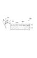
図1は、本発明の第1実施形態に係る貼り合わせ基板10Aの構成を示す断面図である。本実施形態の貼り合わせ基板10Aは、GaN単結晶からなるGaN薄層12を、支持基板14の主面14aに貼り合わせた構成を備える。支持基板14は、窒化物系化合物半導体とは異なる材料であって、可視光に対して透明であり且つ導電性を有する材料、例えばβ−Ga2O3あるいはZnOに不純物がドープされることによって得られる。β−Ga2O3は、260[nm]以上の波長域の光に対して透明であり、ZnOは、365[nm]以上の波長域の光に対して透明である。不純物は、例えばSiである。この貼り合わせ基板10AではGaN薄層12上に発光層等が結晶成長されるので、支持基板14の結晶状態は、単結晶であってもよく、多結晶であってもよい。また、十分な導電性を確保して高い電流効率の発光素子を作製するために、支持基板14の比抵抗は、3×10⁻³[Ωcm]以上1[Ωcm]以下であることが好ましい。(First embodiment)
FIG. 1 is a cross-sectional view showing a configuration of a bonded
GaN薄層12は、その平均転位密度が1×107[cm−2]以下といった極めて結晶性の良いGaN単結晶からなる層である。GaN薄層12の表面12aは、GaN単結晶のC面に対して傾斜しており、GaN結晶における非極性面(無極性面)または半極性面となっている。GaN薄層12の表面12aは、GaN単結晶のC面に対してM軸又はA軸の方向に傾斜していることが好ましい。GaN薄層12の表面12aの傾斜角は、表面12aの法線軸Nxを示す法線ベクトルNVと、GaN結晶のC軸方向を示すC軸ベクトルVCとの成す角度αによって規定される。この角度αは、GaN結晶のC軸に直交する基準平面Rx(すなわち{0001}面又は{000−1}面)に対して50°以上110°以下の範囲内にあることができ、より好ましくは60°以上95°以下の範囲内にあることができる。角度αが50°以下または110°以上である場合、表面12a上に成長すべき発光層がInを含む場合にピエゾ分極による影響が大きくなり、また発光層にInを十分に取り込めないおそれもあるので、青色領域からの十分な長波長化と高輝度化とを同時に達成するには、角度αが上記範囲内にあることが好ましい。特に、60°以上95°以下の範囲内であることにより、Inを含む発光層において生じるピエゾ分極を効果的に低減でき、発光効率をより高めることができる。The GaN
更に、この角度αは、70°以上80°以下の範囲内、換言すれば75°±5°の範囲内にあることが好適である。表面12aが半極性面となるこの角度範囲によれば、500[nm]以上550[nm]以下といった長波長の光を発生するための発光層に好適なインジウム組成のInGaN層を提供でき、ピエゾ分極をより効果的に低減できる。 Furthermore, this angle α is preferably in the range of 70 ° to 80 °, in other words, in the range of 75 ° ± 5 °. According to this angular range in which the
更に好適には、GaN薄層12の表面12aは、GaN単結晶の{20−21}面(すなわち、GaN単結晶のC面からM軸方向に75°傾斜した面)であるか、または{20−21}面に対して±3°以内の傾斜角をもって形成されると良い。或いは、表面12aは、GaN単結晶のM面であるか、またはM面に対して±5°以内の傾斜角をもって形成されると良い。或いは、表面12aは、GaN単結晶のA面であるか、またはA面に対して±5°以内の傾斜角をもって形成されると良い。 More preferably, the
続いて、本実施形態に係る貼り合わせ基板10Aの製造方法の一例について説明する。まず、支持基板14として、β−Ga2O3基板を作製する。β−Ga2O3単結晶は、例えばチョクラルスキー法や、EFG(Edge-definedFilm-fed Growth)法、FZ(Floating Zone)法といった各種の溶融成長法によって作製される。チョクラルスキー法の場合、次のようにしてβ−Ga2O3単結晶を作製する。坩堝内にGa2O3原料を投入し、融点である1725℃以上の温度で加熱して溶融させる。次に、坩堝の上方に配置した種結晶に接触させて冷却し、凝固による結晶成長を促す。そして、坩堝を回転させながら種結晶を上方に引き上げることにより、β−Ga2O3単結晶インゴットが得られる。この結晶成長の際の雰囲気は、金属製坩堝が酸化しないように、且つ、β−Ga2O3が還元しないように、例えば酸素及び水素の混合雰囲気であることが好ましい。また、坩堝内にSi、Snなどのドーパントを添加することにより、導電性を有するβ−Ga2O3結晶が得られる。こうして作製されるβ−Ga2O3単結晶インゴットをスライスし、研磨加工を施すことにより、支持基板14としてのβ−Ga2O3基板が得られる。Then, an example of the manufacturing method of the bonded
また、上記工程とは別に、GaN薄層12の元となるGaN基板を準備する。このGaN基板の表面は、GaN結晶のC面に対する主面の傾斜角が50°以上且つ110°以下である非極性面または半極性面となっている。このGaN基板の表面に、イオン注入装置を用いて水素イオンを打ち込む。なお、打ち込むイオンとしては、水素イオンに限らず様々なものを使用できる。水素イオンを例えば1×10¹⁷[cm−2]程度の密度になるまで注入すると、GaN基板の表面から深さ数百ナノメートルの領域に、ダメージ層が生じる。このダメージ層付近は、水素イオンの濃度が極めて高くなっている。In addition to the above steps, a GaN substrate serving as the base of the GaN
続いて、イオン注入したGaN基板の表面とβ−Ga2O3基板の主面とを互いに貼り合わせる。その貼り合わせ方法としては、様々な方法がある。例えば、超高真空中で両基板を押圧して貼り合わせてもよく、或いは、低真空のプラズマ雰囲気の中で、200℃程度の加熱を行って貼り合わせても良い。そして、貼り合わせた後に、更に高い温度(例えば300℃〜500℃)で加熱することにより、GaN基板のダメージ層付近の領域から剥離を生じさせる。これにより、GaN基板のうちβ−Ga2O3基板と接する表面を含む部分を層状に残して、GaN基板の他の部分を分離させ、除去する。その結果、β−Ga2O3基板(支持基板14)の上に、GaN薄層12がイオン注入した側と反対側の面を表面にして張り付いた貼り合わせ基板10Aが得られる。この時、イオン注入した基板表面の面指数が(H K L −M)面であれば(ここでH,K,L,Mは自然数)、貼り合わせ基板のGaN薄層の表面は(H K L M)面となる。Subsequently, the surface of the ion-implanted GaN substrate and the main surface of the β-Ga2 O3 substrate are bonded together. There are various methods for the bonding. For example, both substrates may be pressed and bonded together in an ultra-high vacuum, or may be bonded by heating at about 200 ° C. in a low vacuum plasma atmosphere. And after bonding, it peels from the area | region of the damage layer vicinity of a GaN board | substrate by heating at a still higher temperature (for example, 300 to 500 degreeC). This separates and removes the other part of the GaN substrate, leaving a portion of the GaN substrate including the surface in contact with the β-Ga2 O3 substrate in a layered form. As a result, a bonded substrate 10 </ b> A is obtained in which the GaN
以上に説明した、本実施形態に係る貼り合わせ基板10A及びその製造方法によって得られる作用効果について説明する。この貼り合わせ基板10Aにおいては、窒化物系化合物半導体とは異なる材料からなる支持基板14の主面14aに、GaN薄層12が貼り合わされている。これにより、基板一枚あたりのGaNの厚さを低減できるので、GaN結晶から成る表面を有する基板を一つのGaN単結晶インゴットからより多く作製することができ、基板の製造コストを抑えることができる。特に、本実施形態の場合、GaN単結晶の非極性面または半極性面を貼り合わせ基板10Aの表面に有するが、このような面を有するGaN基板を作製しようとすると、C面を主面とするGaN基板と比較して一つのGaN単結晶インゴットから取り出せる枚数が少なくなる。したがって、本実施形態に係る貼り合わせ基板10Aのコスト低減効果は、GaN単結晶の非極性面または半極性面を表面に有する場合に、より効果的である。 The effects obtained by the bonded
また、GaN薄層12が、GaN結晶のC面に対し50°以上110°以下の傾斜角をもって形成された表面12aを有することにより、GaN結晶の非極性面または半極性面を表面に有する基板を提供できる。発光層といった窒化物系化合物半導体層は、GaN薄層12の結晶方位を引き継いで成長するので、GaN薄層12の表面12aが非極性面または半極性面であることにより、発光層にInが含まれる場合であってもピエゾ分極が抑えられ、例えば青色や緑色といった波長の光を効率よく出力することができる。 Further, the GaN
更に、支持基板14は可視光に対して透明で且つ導電性を有するβ−Ga2O3やZnOによって構成されているが、この支持基板14の主面14aはGaN薄層12によって保護されているため、その上に窒化物系化合物半導体を高温で成長させたとしても支持基板14を安定に保つことができる。したがって、基板上に成長する窒化物系化合物半導体の結晶品質を良好にできる。すなわち、本実施形態の貼り合わせ基板10Aによれば、ZnO基板やβ−Ga2O3基板といった透明導電性基板の上に窒化物系化合物半導体層が設けられた発光素子を好適に実現できる。これにより、透明基板である支持基板14を介して光を効率的に取り出すことができる。更に、支持基板14が導電性であることにより、貼り合わせ基板10Aの表面側と裏面側とにそれぞれ電極を形成することができるので、素子の縦方向に電流を流すことが可能となる。これにより、電極の総面積を小さくすることができ、発光素子の低コスト化を図ることができる。Further, the
また、本実施形態のように、支持基板14はβ−Ga2O3基板またはZnO基板であることが好ましい。これにより、可視光に対して透明な導電性の支持基板14を好適に実現できる。Further, as in this embodiment, the
また、本実施形態のように、GaN薄層12の平均転位密度は1×10⁷[cm−2]以下であることが好ましい。これにより、GaN薄層12上に成長する窒化物系化合物半導体層の結晶品質を高め、発光効率を向上させることができる。このようなGaN薄層12は、主面の平均転位密度が1×10⁷[cm−2]以下である低転位GaN基板を貼り合わせ基板10Aの作製に用いることにより実現できる。なお、このような低転位のGaN基板は極めて高価であるが、GaN薄層12としてその僅かな部分を用いて貼り合わせ基板10Aを作製することにより、一枚当たりの製造コストを効果的に低減できる。In addition, as in the present embodiment, the average dislocation density of the GaN
また、上述したように、GaN薄層12の表面12aの傾斜方向は、A軸方向またはM軸方向であることが好ましい。傾斜方向がA軸方向である場合、M面は表面に対して常に垂直となるので、この貼り合わせ基板10AをM面で劈開し、例えばレーザ素子の光共振端面として利用することが可能となる。同様に、傾斜方向がM軸方向である場合、A面は表面に対して常に垂直となるので、この貼り合わせ基板10AをA面で劈開し、光共振端面として利用することが可能となる。 Further, as described above, the inclination direction of the
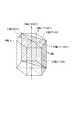
このような貼り合わせ基板10Aの劈開の観点から、貼り合わせ基板10Aにも好適な面方位が存在する。ここで、図2は、ZnOの結晶構造を示す図であり、図3は、β−Ga2O3の結晶構造を示す図である。From the viewpoint of such cleavage of the bonded
図2に示すように、ZnOは、六方晶系のウルツ鉱型の結晶構造を有している。六方晶における六角形の中心から頂点に向かう軸をA軸<11−20>、これに垂直な軸をM軸<1−100>とし、A面(11−20)及びM面(1−100)は、それぞれA軸及びM軸に垂直であり、A軸及びM軸の双方に垂直な軸をC軸、C軸<0001>に垂直な面をC面(0001)とする。なお、六方晶のM軸(A軸)は120度ごとに3方向に存在する。なお、このような六方晶系のウルツ鉱構造を有するZnOの格子定数は、A軸が0.325[nm]、C軸が0.521[nm]である。 As shown in FIG. 2, ZnO has a hexagonal wurtzite crystal structure. The axis from the hexagonal center to the apex in the hexagonal crystal is defined as the A axis <11-20>, and the axis perpendicular thereto is defined as the M axis <1-100>. The A plane (11-20) and the M plane (1-100) ) Are perpendicular to the A axis and the M axis, respectively, the axis perpendicular to both the A axis and the M axis is defined as the C axis, and the plane perpendicular to the C axis <0001> is defined as the C plane (0001). The hexagonal M-axis (A-axis) exists in three directions every 120 degrees. Note that the lattice constant of ZnO having such a hexagonal wurtzite structure is 0.325 [nm] for the A axis and 0.521 [nm] for the C axis.
また、図3に示すように、β−Ga2O3は、単斜晶系の結晶構造を有している。単斜晶系酸化ガリウムの結晶格子のa軸、b軸及びc軸の格子定数は、それぞれ、1.22[nm]、0.30[nm]及び0.58[nm]である。ベクトルVa、Vb及びVcは、それぞれ、a軸、b軸及びc軸の方向を示す。ベクトルVa及びVbは(001)面を規定し、ベクトルVb、Vcは(100)面を規定し、ベクトルVc及びVaは(010)面を規定する。ベクトルVa及びVbの成す角度γ及びベクトルVb及びVcの成す角度αは90度であり、ベクトルVc及びVaの成す角度βは103.7度である。Further, as shown in FIG. 3, β-Ga2 O3 has a monoclinic crystal structure. The lattice constants of the a-axis, b-axis, and c-axis of the monoclinic gallium oxide crystal lattice are 1.22 [nm], 0.30 [nm], and 0.58 [nm], respectively. Vectors Va, Vb, and Vc indicate the directions of the a-axis, b-axis, and c-axis, respectively. The vectors Va and Vb define the (001) plane, the vectors Vb and Vc define the (100) plane, and the vectors Vc and Va define the (010) plane. The angle γ formed by the vectors Va and Vb and the angle α formed by the vectors Vb and Vc are 90 degrees, and the angle β formed by the vectors Vc and Va is 103.7 degrees.
本実施形態において、支持基板14がZnO基板である場合、支持基板14の主面14aの面方位は{0001}面であることが好ましい。この場合、劈開面である{1−100}面(すなわちM面)及び{11−20}面(すなわちA面)がそれぞれ主面14aと垂直になるので、主面14aと垂直な面でもって支持基板14を精度よく劈開することができ、例えばレーザ素子の共振端面を精度よく形成できる。 In the present embodiment, when the
また、支持基板14がβ−Ga2O3基板である場合、支持基板14の主面14aの面方位は、{100}面、{010}面、{001}面、(100)面から[00−1]方向へ13.7°傾いた面、及び(001)面から[−100]方向へ13.7°傾いた面のうちいずれかであることが好ましい。主面14aが{100}面である場合、劈開面である{001}面が主面14aと垂直になる。主面14aが{010}面である場合、劈開面である{100}面及び{001}面が主面14aと垂直になる。主面14aが{100}面である場合、劈開面である{001}面が主面14aと垂直になる。主面14aが(100)面から[00−1]方向へ13.7°傾いた面である場合、劈開面である{001}面及び{010}面の双方が主面14aと垂直になる。また、主面14aが(001)面から[−100]方向へ13.7°傾いた面である場合、劈開面である{100}面及び{010}面の双方が主面14aと垂直になる。したがって、主面14aと垂直な面でもって支持基板14を精度よく劈開することができ、例えばレーザ素子の共振端面を精度よく形成できる。When the
また、上記のように支持基板14の劈開面が主面14aと垂直である場合には、GaN薄層12の劈開方向と、支持基板14の劈開方向とが互いに揃っている(実質的に平行である)ことが尚好ましい。GaN薄層12の劈開方向と、支持基板14の劈開方向とを互いに合致させておくことにより、レーザ素子を作製する際に、良好な劈開面による共振端面を作製することができ、高品質のレーザ素子を作製できるからである。また、たとえGaN薄層12の共振器面が良好な劈開面が得易い面と異なっていても、支持基板14の劈開面に従って比較的良好な共振器面を得ることができる。 When the cleavage surface of the
具体的には、支持基板14がZnO基板であり、支持基板14の主面14aの面方位が{0001}面である場合、GaN薄層12の<1−100>方向または<11−20>方向と、ZnO結晶の<1−100>方向または<11−20>方向とが互いに並行であることが好ましい。例えば、表面12aがA軸方向に傾斜したGaN薄層12の<1−100>方向が支持基板14のZnO結晶の<1−100>方向または<11−20>方向と並行であることにより、GaN薄層12の劈開方向と支持基板14の劈開方向とが揃うことができる。或いは、表面12aがM軸方向に傾斜したGaN薄層12の<11−20>方向が支持基板14のZnO結晶の<1−100>方向または<11−20>と並行であることにより、GaN薄層12の劈開方向と支持基板14の劈開方向とが揃うことができる。 Specifically, when the
また、支持基板14がβ−Ga2O3基板であり、支持基板14の主面14aの面方位が{010}面である場合、GaN薄層12の<1−100>方向または<11−20>方向と、β−Ga2O3結晶の{100}面または{001}面の面方向とが互いに並行であることが好ましい。また、支持基板14の主面14aの面方位が(100)面から[00−1]方向へ13.7°傾いた面である場合、GaN薄層12の<1−100>方向または<11−20>方向と、β−Ga2O3結晶の{001}面の面方向とが互いに並行であることが好ましい。また、支持基板14の主面14aの面方位が(001)面から[−100]方向へ13.7°傾いた面である場合、GaN薄層12の<1−100>方向または<11−20>方向と、β−Ga2O3結晶の{100}面の面方向とが互いに並行であることが好ましい。When the
(第2の実施の形態)
図4は、本発明の第2実施形態に係る貼り合わせ基板10Bの構成を示す断面図である。本実施形態の貼り合わせ基板10Bは、第1実施形態のGaN薄層12上に、窒化物系化合物半導体積層部16が設けられた構成を備える。窒化物系化合物半導体積層部16は、GaN薄層12の表面12a上にエピタキシャル成長されたn型(第1導電型)半導体層18と、n型半導体層18上にエピタキシャル成長された発光層20と、発光層20上にエピタキシャル成長されたp型(第2導電型)半導体層22とを含む。なお、n型半導体層18は、本実施形態における第1窒化物系化合物半導体層であり、p型半導体層22は、本実施形態における第2窒化物系化合物半導体層である。(Second Embodiment)
FIG. 4 is a cross-sectional view showing a configuration of a bonded
n型半導体層18は、例えばn型のGaN系半導体、典型的にはn型GaNからなることができる。n型半導体層18は、例えば下部クラッド層として機能する。p型半導体層22は、例えばp型のGaN系半導体、典型的にはp型GaNからなることができる。p型半導体層22は、例えば上部クラッド層として機能する。 The n-
また、発光層20は、Inを含む単一層からなることができ、或いは量子井戸構造を有することができる。必要な場合には、量子井戸構造は、交互に配列された井戸層及び障壁層を含むことができる。井戸層はInを含む窒化物系化合物半導体、例えばInGaN等からなることができ、障壁層は井戸層よりバンドギャップエネルギーの大きいInGaN又はGaN等からなることができる。発光層20の発光波長は、井戸層のバンドギャップやIn組成、その厚さ等によって制御される。本実施形態のGaN薄層12の表面12aが非極性面または半極性面であることにより、発光層20は、波長500[nm]以上550[nm]以下の範囲のピーク波長を有する緑色光を発生するようなIn組成とされることができる。 In addition, the
本実施形態の貼り合わせ基板10Bによれば、GaN単結晶の非極性面または半極性面を表面に有する基板の製造コストを抑えることができ、且つ、ZnO基板やβ−Ga2O3基板といった透明導電性基板の上に窒化物系化合物半導体層が設けられた構造を備える発光素子の製造に適した基板を提供できる。According to the bonded
なお、本実施形態に係る貼り合わせ基板10Bを作製する際には、第1実施形態において説明した貼り合わせ基板10Aを作製したのち、そのGaN薄層12の表面12a上に、n型半導体層18、発光層20、及びp型半導体層22を順にMOCVD法によりエピタキシャル成長させる。その際、n型半導体層18とGaN薄層12とが接するように、n型半導体層18をGaN薄層12の直上に成長させることができる。また、n型半導体層18、発光層20、及びp型半導体層22を、水素還元雰囲気や高濃度のアンモニアガス雰囲気において、900℃以上1150℃以下という高い成長温度で成長させることができる。このように、GaN薄層12の直上に窒化物系化合物半導体を高温で成長させた場合であっても、ZnO基板やβ−Ga2O3基板といった支持基板14がGaN薄層12に保護され、支持基板14を安定に保持できる。したがって、n型半導体層18、発光層20、及びp型半導体層22の結晶性を良好にできる。When manufacturing the bonded
(第3の実施の形態)
図5は、本発明に係る発光素子に関する第3実施形態として、半導体レーザ素子30の構成を示す断面図である。図5を参照すると、半導体レーザ素子30は、第1実施形態の貼り合わせ基板10Aがチップ状に切断されて成る基板31を備えている。基板31は、GaN薄層12及び支持基板14からなる貼り合わせ基板である。(Third embodiment)
FIG. 5 is a cross-sectional view showing a configuration of a
半導体レーザ素子30は、レーザ発振のための光導波路60を有する。また、半導体レーザ素子30は、GaN薄層12の表面12a上に設けられたn型クラッド層55と、n型クラッド層55上に設けられた発光層57と、発光層57上に設けられたp型クラッド層59とを有する。 The
n型クラッド層55は、光導波路60の一部を構成する第1窒化物系化合物半導体層である。n型クラッド層55はn型のGaN系半導体からなり、例えばGaN、AlGaN、InAlGaN等からなることができる。n型クラッド層55は、900℃以上1150℃以下という高い成長温度でGaN薄層12の直上にエピタキシャル成長された層である。p型クラッド層59は、光導波路60の一部を構成する第2窒化物系化合物半導体層である。p型クラッド層59はp型のGaN系半導体からなり、例えばGaN、AlGaN、InAlGaN等からなることができる。なお、発光層57の構成は第2実施形態の発光層20と同様であるため、その詳細な説明を省略する。 The n-
また、半導体レーザ素子30は、n型クラッド層55と発光層57との間に、第1光ガイド層61を更に備える。半導体レーザ素子30は、発光層57とp型クラッド層59との間に、第2光ガイド層63を更に備える。第1光ガイド層61及び第2光ガイド層63は、基板31に光を逃がすことなく発光層57付近に光を閉じ込め、しきい値電流を低減する為に設けられる。 The
第1光ガイド層61は、GaN又はInGaNからなる第1の層71と、InGaNからなる第2の層73とを含むことができる。第1の層71はn型クラッド層55上に設けられ、第2の層73は第1の層71と発光層57との間に設けられる。なお、第2の層73のIn組成は、第1の層71のIn組成より大きく、発光層57内のInGaN井戸層のIn組成より小さい。一実施例では、第1の層71はn型GaNからなり、第2の層73はアンドープInGaNからなることができる。 The first light guide layer 61 can include a
第2光ガイド層63は、GaN又はInGaNからなる第1の層75と、InGaNからなる第2の層77とを含むことができる。第1の層75は発光層57上に設けられ、第2の層77は発光層57と第1の層75との間に設けられる。なお、第2の層77のIn組成は、第1の層75のIn組成より大きく、発光層57内のInGaN井戸層のIn組成より小さい。一実施例では、第1の層75はp型GaNからなり、第2の層77はアンドープInGaNからなる。 The second light guide layer 63 can include a first layer 75 made of GaN or InGaN and a
半導体レーザ素子30は、電子ブロック層67を更に備える。本実施形態では、電子ブロック層67は第1の層75と第2の層77との間に設けられている。電子ブロック層67は例えばp型AlGaNからなることができる。 The
半導体レーザ素子30は、p型クラッド層59上に設けられたp型コンタクト層81を更に備える。p型コンタクト層81は、例えばGaN、AlGaN等からなることができる。p型クラッド層59の一部、及びp型コンタクト層81は所定の光導波方向に延びるリッジ形状をしており、該リッジ形状の側面およびp型クラッド層59の表面は絶縁膜87によって覆われている。このリッジの延伸方向、すなわち光導波路60の光導波方向は、GaN薄層12及び支持基板14の劈開方向に対して垂直に延びている。 The
具体的には、GaN薄層12の表面12aがGaN単結晶のM軸方向に傾斜している場合、光導波路60はGaN薄層12の<11−20>方向に沿って設けられる。そして、支持基板14がβ−Ga2O3基板であるときには、GaN薄層12の<11−20>方向がβ−Ga2O3結晶の{100}面もしくは{001}面と垂直に交差するように、基板31が作製される。これにより、光導波路60の光導波方向とGaN薄層12及び支持基板14の劈開面とが垂直に交差し、良好な共振端面を得ることができる。Specifically, when the
半導体レーザ素子30は、アノード電極85を更に備える。アノード電極85は光導波路60のリッジ上に設けられており、絶縁膜87の開口を介してp型コンタクト層81に接触している。また、半導体レーザ素子30は、カソード電極99を更に備える。カソード電極99は、支持基板14の裏面14b上に設けられる。 The
本実施形態に係る半導体レーザ素子30によれば、第1実施形態に係る貼り合わせ基板10Aと同一の構造(GaN薄層12および支持基板14)を含むので、基板31の製造コストを抑えることができる。また、n型クラッド層55、発光層57およびp型クラッド層59等を支持基板14上に高温で成長させたとしても、GaN薄層12によって支持基板14を保護するので、支持基板14を安定に保つことができ、これらの半導体層の結晶品質を良好にできる。すなわち、本実施形態の半導体レーザ素子30によれば、ZnO基板やβ−Ga2O3基板といった透明導電性基板の上に窒化物系化合物半導体層が設けられた半導体レーザ素子を好適に実現できる。The
また、第1実施形態において説明したように、GaN結晶のC面に対し50°以上110°以下の傾斜角をもって形成されたGaN薄層12の表面12a、すなわちGaN結晶の非極性面または半極性面上にn型クラッド層55、発光層57およびp型クラッド層59がエピタキシャル成長しているので、Inを含む発光層57におけるピエゾ分極の影響を低減し、発光効率を高めることができる。 Further, as described in the first embodiment, the
(第4の実施の形態)
図6は、本発明に係る発光素子に関する第4実施形態として、発光ダイオード(LED)40の構成を示す断面図である。図6を参照すると、発光ダイオード40は、第1実施形態の貼り合わせ基板10Aがチップ状に切断されて成る基板41を備えている。基板41は、GaN薄層12及び支持基板14からなる貼り合わせ基板である。(Fourth embodiment)
FIG. 6 is a cross-sectional view showing a configuration of a light emitting diode (LED) 40 as a fourth embodiment related to the light emitting element according to the present invention. Referring to FIG. 6, the
また、発光ダイオード40は、GaN薄層12の表面12a上に順に積層されたn型GaN層42及びn型AlGaN層43といった第1導電型の窒化物系化合物半導体層を備えている。n型GaN層42は、900℃以上1150℃以下という高い成長温度でGaN薄層12の直上に成長された層である。また、発光ダイオード40は、n型AlGaN層43上に設けられた発光層44を備えている。また、発光ダイオード40は、発光層44上に順に積層されたp型AlGaN層45及びp型GaN層46といった第2導電型の窒化物系化合物半導体層を備えている。なお、発光層44の構成は、第2実施形態の発光層20と同様であるため詳細な説明を省略する。 The
発光ダイオード40は、アノード電極47及びカソード電極48を更に備えている。アノード電極47は、p型GaN層46上に設けられている。アノード電極47は例えばNi/Au/Al/Auといった金属を順次積層してなり、アノード電極47とp型GaN層46との間でオーミック接触が実現されている。カソード電極48は、導電性の支持基板14の裏面14b上に設けられている。カソード電極48は、例えばTi/Al/Auといった金属を順次積層してなり、カソード電極48と支持基板14との間でオーミック接触が実現されている。 The
本実施形態に係る発光ダイオード40は、上述した第3実施形態と同様に、貼り合わせ基板10Aと同一の構造(GaN薄層12および支持基板14)を含むので、基板31の製造コストを抑えることができる。また、n型GaN層42、発光層44およびp型GaN層46等を支持基板14上に高温で成長させたとしても、GaN薄層12によって支持基板14を保護するので、支持基板14を安定に保つことができ、これらの半導体層の結晶品質を良好にできる。すなわち、本実施形態の発光ダイオード40によれば、ZnO基板やβ−Ga2O3基板といった透明導電性基板の上に窒化物系化合物半導体層が設けられた発光ダイオードを好適に実現できる。Since the
また、本実施形態においても、GaN結晶のC面に対し50°以上110°以下の傾斜角をもって形成されたGaN薄層12の表面12a、すなわちGaN結晶の非極性面または半極性面上にn型GaN層42、発光層44およびp型GaN層46がエピタキシャル成長しているので、Inを含む発光層44におけるピエゾ分極の影響を低減し、発光効率を高めることができる。 Also in this embodiment, n is formed on the
(実施例1)
HVPEにより気相合成された、(0001)面を主面とするGaN基板を種結晶として、その上に、HVPEによりGaN結晶を厚く成長した。そして、15[mm]程度の厚さのGaN単結晶インゴットを得た。そのGaN単結晶インゴットに対し種々の面方位でスライス加工を行い、半極性面を有する複数のGaN基板を得た。その後、これらのGaN基板の−C面すなわち(000−1)面に近い側の面を主面として研磨加工し、更に洗浄を施した。こうして得られたGaN基板の主面の面方位は、−C面すなわち(000−1)面に対するM軸方向への傾斜角が30°、60°、70°、75°、80°、及び85°であった。Example 1
A GaN substrate having a (0001) plane as a main surface and synthesized by HVPE was used as a seed crystal, and a GaN crystal was grown thickly by HVPE. Then, a GaN single crystal ingot having a thickness of about 15 [mm] was obtained. The GaN single crystal ingot was sliced in various plane orientations to obtain a plurality of GaN substrates having semipolar planes. After that, the GaN substrate was polished by using the surface close to the -C plane, that is, the (000-1) plane, and further washed. As for the surface orientation of the main surface of the GaN substrate thus obtained, the inclination angles in the M-axis direction with respect to the −C plane, that is, the (000-1) plane are 30 °, 60 °, 70 °, 75 °, 80 °, and 85 °.
これらのGaN基板をイオン注入装置にセットし、主面に対してイオン注入を行った。具体的には、水素イオンを加速電圧50[KeV]でもってGaN基板の主面すなわち窒素面側に注入した。イオン注入中、GaN基板の基板温度を200℃程度に昇温した。これにより、水素イオンのドーズ量を7×10¹⁷[cm−2]として、GaN基板の主面から深さ約200[nm]程度の位置にドーズ量のピークが見られた。このドーズ量のピーク付近が、イオン注入によるダメージ層である。イオン注入後、GaN基板の主面を洗浄した。そして、GaN基板をドライエッチング装置にセットして、N2ガス雰囲気中で放電により生成したプラズマに曝し、GaN基板の主面を清浄面とした。なお、このときのドライエッチング条件は、RFパワーが100[W]、N2ガス流量が50[sccm(1分当たりの標準立方センチメートル)]、N2ガス分圧が13.3[Pa]であった。These GaN substrates were set in an ion implantation apparatus, and ion implantation was performed on the main surface. Specifically, hydrogen ions were implanted into the main surface of the GaN substrate, that is, the nitrogen surface side with an acceleration voltage of 50 [KeV]. During the ion implantation, the substrate temperature of the GaN substrate was raised to about 200 ° C. Thereby, the dose amount of hydrogen ions was set to 7 × 10¹⁷ [cm−2 ], and a peak of the dose amount was observed at a position of about 200 [nm] in depth from the main surface of the GaN substrate. The vicinity of the peak of the dose amount is a damaged layer caused by ion implantation. After ion implantation, the main surface of the GaN substrate was cleaned. Then, the GaN substrate was set in a dry etching apparatus and exposed to plasma generated by discharge in an N2 gas atmosphere, so that the main surface of the GaN substrate was a clean surface. The dry etching conditions at this time were RF power of 100 [W], N2 gas flow rate of 50 [sccm (standard cubic centimeter per minute)], and N2 gas partial pressure of 13.3 [Pa]. It was.
また、支持基板として、ZnO基板及びβ−Ga2O3基板の両方を用意した。ZnO基板は、ZnO結晶のC面を主面とするn導電型の基板であり、比抵抗は1×10⁻²[Ωcm]であった。また、β−Ga2O3基板は、β−Ga2O3結晶の(001)面を主面とする基板であり、比抵抗は1×10⁻²[Ωcm]であった。これら支持基板の主面を十分に洗浄した後、O2ガス雰囲気中で放電により生成したプラズマに曝し、支持基板の主面を清浄面とした。なお、このときのドライエッチング条件は、RFパワーが100[W]、O2ガス流量が50[sccm]、O2ガス分圧が6.7[Pa]であった。In addition, both a ZnO substrate and a β-Ga2 O3 substrate were prepared as support substrates. The ZnO substrate was an n-conductivity type substrate having a C-plane of ZnO crystal as the main surface, and the specific resistance was 1 × 10⁻² [Ωcm]. The β-Ga2 O3 substrate was a substrate having a (001) plane of β-Ga2 O3 crystal as a main surface, and the specific resistance was 1 × 10⁻² [Ωcm]. After sufficiently cleaning the main surfaces of these support substrates, they were exposed to plasma generated by discharge in an O2 gas atmosphere to make the main surfaces of the support substrates clean surfaces. The dry etching conditions at this time were RF power of 100 [W], O2 gas flow rate of 50 [sccm], and O2 gas partial pressure of 6.7 [Pa].
その後、GaN基板の主面と、ZnO基板及びβ−Ga2O3基板の主面とを、表面活性化法により貼り合わせた。なお、このとき、一旦大気中にて貼り合わせた後に、室温から200℃〜300℃に昇温加熱して、接着強度を増加させた。Thereafter, the main surface of the GaN substrate and the main surfaces of the ZnO substrate and the β-Ga2 O3 substrate were bonded together by a surface activation method. In addition, at this time, after pasting together in air | atmosphere, it heated up from room temperature to 200 to 300 degreeC, and increased the adhesive strength.
次に、これらの基板を貼り合わせた状態で500℃まで昇温し、GaN基板とZnO基板またはβ−Ga2O3基板との接合物に対して斜め方向から荷重を加えることにより、GaN基板と、ZnO基板及びβ−Ga2O3基板とを分離させた。その際、GaN基板のうちダメージ層より主面側に位置する層状部分がGaN基板から分離され、ZnO基板上およびβ−Ga2O3基板上にGaN薄層として転写された。その結果、ZnO基板およびβ−Ga2O3基板の各主面上に、厚さ約200[nm]程度のGaN薄層が形成された。なお、GaN薄層が分離した残りのGaN基板は、再び貼り合わせ基板の材料として使用可能である。Next, the temperature is raised to 500 ° C. in a state where these substrates are bonded together, and a load is applied from an oblique direction to the joint between the GaN substrate and the ZnO substrate or the β-Ga2 O3 substrate, whereby a GaN substrate is obtained. And the ZnO substrate and the β-Ga2 O3 substrate were separated. At that time, the layered portion located on the main surface side of the damaged layer in the GaN substrate was separated from the GaN substrate and transferred as a GaN thin layer on the ZnO substrate and the β-Ga2 O3 substrate. As a result, a thin GaN layer having a thickness of about 200 [nm] was formed on each main surface of the ZnO substrate and the β-Ga2 O3 substrate. The remaining GaN substrate from which the GaN thin layer has been separated can be used again as a material for the bonded substrate.
こうして、ZnO基板のC面上に、GaN結晶のC面に対してM軸方向に0°、10°、30°、60°、70°、75°、80°、及び85°それぞれ表面が傾斜したGaN薄層を有する貼り合わせ基板が得られた。すなわち、研磨してイオン注入した主面の裏側の面が貼り合わせ基板の表面側に存在している。同様に、β−Ga2O3基板の(001)面上に、GaN結晶のC面に対してM軸方向に0°、10°、30°、60°、70°、75°、80°、及び85°それぞれ表面が傾斜したGaN薄層を有する貼り合わせ基板が得られた。これも、研磨してイオン注入した主面の裏側の面が貼り合わせ基板の表面側に存在している。なお、ZnO基板及びβ−Ga2O3基板において、その面方位を他のものに変えても、同様にGaN薄層を貼り合わせることができた。Thus, on the C plane of the ZnO substrate, the surface is inclined at 0 °, 10 °, 30 °, 60 °, 70 °, 75 °, 80 °, and 85 ° in the M-axis direction with respect to the C plane of the GaN crystal. A bonded substrate having a thin GaN layer was obtained. That is, the back surface of the main surface polished and ion-implanted exists on the surface side of the bonded substrate. Similarly, 0 °, 10 °, 30 °, 60 °, 70 °, 75 °, 80 ° in the M-axis direction with respect to the C-plane of the GaN crystal on the (001) plane of the β-Ga2 O3 substrate. A bonded substrate having a GaN thin layer whose surfaces are inclined by 85 ° and 85 ° was obtained. Also in this case, the back surface of the main surface polished and ion-implanted exists on the surface side of the bonded substrate. Note that, in the ZnO substrate and the β-Ga2 O3 substrate, the GaN thin layer could be similarly bonded even if the plane orientation was changed to another.
(実施例2)
本実施例では、実施例1において得られた貼り合わせ基板上に、GaN薄膜をMOCVD法によりエピタキシャル成長させた。(Example 2)
In this example, a GaN thin film was epitaxially grown on the bonded substrate obtained in Example 1 by MOCVD.
具体的には、実施例1において作製した貼り合わせ基板をMOCVD成長炉にセットし、V族原料としてNH3ガスをH2キャリアガス中に流すとともに、III族原料としてTMG(トリメチルガリウム)を水素ガスで希釈して貼り合わせ基板に吹き付けるように流し、基板温度を1030℃に保って、GaN薄膜のエピタキシャル成長を行った。なお、このGaN薄膜の成長時に、Siドーピングのためのシラン(SiH4)を水素ガスで希釈して流し、GaN薄膜中へのn型ドーピングを行った。通常、ZnO基板やβ−Ga2O3基板の直上に、MOCVD法によりGaN薄膜をエピタキシャル成長させると、水素キャリアガスの還元雰囲気やNH3ガスの反応性によって基板表面がダメージを受け、その上に成長するGaN薄膜は、剥がれや品質の劣化を伴うこととなる。しかしながら、本実施例では、ZnO基板やβ−Ga2O3基板のダメージは全く認められず、良好な結晶品質を有する厚さ2[μm]のGaNエピタキシャル薄膜を成長させることができた。これは、比較的低温でもって予めGaN薄層がZnO基板やβ−Ga2O3基板に貼り付けられていたために、このGaN薄層が保護層として働き、雰囲気ガスによる基板の損傷を抑止したものと考えられる。Specifically, the bonded substrate prepared in Example 1 is set in a MOCVD growth furnace, and NH3 gas is allowed to flow into the H2 carrier gas as a group V source, and TMG (trimethylgallium) is hydrogenated as a group III source. The GaN thin film was epitaxially grown by diluting with gas and flowing to the bonded substrate and maintaining the substrate temperature at 1030 ° C. During the growth of the GaN thin film, silane (SiH4 ) for Si doping was diluted with hydrogen gas and flowed to perform n-type doping into the GaN thin film. Normally, when a GaN thin film is epitaxially grown directly on a ZnO substrate or β-Ga2 O3 substrate by MOCVD, the substrate surface is damaged by the reducing atmosphere of the hydrogen carrier gas or the reactivity of NH3 gas, The growing GaN thin film is accompanied by peeling and quality deterioration. However, in this example, damage to the ZnO substrate or β-Ga2 O3 substrate was not observed at all, and a GaN epitaxial thin film having a thickness of 2 [μm] having good crystal quality could be grown. This is because the GaN thin layer was affixed to the ZnO substrate or β-Ga2 O3 substrate in advance at a relatively low temperature, and this GaN thin layer worked as a protective layer to suppress damage to the substrate due to atmospheric gas. It is considered a thing.
続いて、このGaN薄膜上に、発光素子を構成する各半導体層を同じMOCVD装置を用いてエピタキシャル成長させた。まず、既に成長されたn型のGaN薄膜上に、n型Alx1Gay1Inz1N層(但し、x1+y1+z1=1、x1≧0、y1≧0、z1≧0)を成長させた。その際、Al原料として有機金属TMAを水素ガスに希釈して流し、In原料として有機金属TMIを水素ガスに希釈して流した。次に、n型Alx1Gay1Inz1N層上に、Alx2Gay2Inz2N(但し、x2+y2+z2=1、x2≧0、y2≧0、z2≧0)からなる井戸層と、井戸層よりバンドギャップの大きいAlx3Gay3Inz3N(但し、x3+y3+z3=1、x3≧0、y3≧0、z3≧0)からなるバリヤ層とを交互に成長させて、単一量子井戸構造あるいは多重量子井戸構造を有する発光層を形成した。さらに、発光層上にp型AlGaN層を成長させ、その上に高濃度のp型GaN層を成長させた。Subsequently, each semiconductor layer constituting the light emitting element was epitaxially grown on the GaN thin film using the same MOCVD apparatus. First, an n-type Alx1 Gay1 Inz1 N layer (x1 + y1 + z1 = 1, x1 ≧ 0, y1 ≧ 0, z1 ≧ 0) was grown on the already grown n-type GaN thin film. At that time, the organometallic TMA was diluted and flowed in hydrogen gas as the Al source, and the organometallic TMI was diluted and flowed in the hydrogen gas as the In source. Next, a well layer made of Alx2 Gay2 Inz2 N (where x2 + y2 + z2 = 1, x2 ≧ 0, y2 ≧ 0, z2 ≧ 0) and a well layer on the n-type Alx1 Gay1 Inz1 N layer A barrier layer composed of Alx3 Gay3 Inz3 N (where x3 + y3 + z3 = 1, x3 ≧ 0, y3 ≧ 0, z3 ≧ 0) having a larger band gap is grown alternately to form a single quantum well structure or multiple layers A light emitting layer having a quantum well structure was formed. Further, a p-type AlGaN layer was grown on the light emitting layer, and a high-concentration p-type GaN layer was grown thereon.
こうして、発光素子としての積層構造を有するエピタキシャルウェハを作製した。C面に対する傾斜角を変化させた何れの貼り合わせ基板においても、このエピタキシャルウェハでのZnO基板及びβ−Ga2O3基板のダメージは見られなかった。また、半導体層の表面にダメージは観察されず、良好な結晶品質を有していた。なお、半導体層の表面状態は、GaN薄層表面のC面に対する傾斜角によって差が見られた。C面に対して75°傾斜させたGaN薄層表面を有する貼り合わせ基板を用いたエピタキシャルウェハが、最も表面状態が良好で且つ平坦であった。Thus, an epitaxial wafer having a laminated structure as a light emitting element was manufactured. In any bonded substrate in which the tilt angle with respect to the C-plane was changed, no damage to the ZnO substrate and β-Ga2 O3 substrate was observed in this epitaxial wafer. Further, no damage was observed on the surface of the semiconductor layer, and the crystal quality was good. The difference in the surface state of the semiconductor layer was observed depending on the inclination angle of the surface of the GaN thin layer with respect to the C-plane. An epitaxial wafer using a bonded substrate having a GaN thin layer surface inclined by 75 ° with respect to the C-plane had the best surface condition and was flat.
(実施例3)
更に、実施例2において作製したエピタキシャルウェハの表面側にp型電極を形成し、裏面側にn型電極を形成して、LEDを作成した。このとき、ウェハをダイシングにより切断して、300[μm]角のチップ形状とした。これらのチップのp型電極とn型電極との間に電流を流したところ、発光層において緑色の発光が見られた。下の表1は、本実施例における、GaN薄層のC面に対する傾斜角と、ブルーシフト量および発光輝度との関係を示す表である。表1に示すように、ブルーシフト量は、GaN薄層のC面に対する傾斜角に依存していた。なお、表1に示す結果から、GaN薄層のC面に対する傾斜角は75°近辺が最も望ましいことがわかる。
Further, a p-type electrode was formed on the front surface side of the epitaxial wafer produced in Example 2, and an n-type electrode was formed on the back surface side to produce an LED. At this time, the wafer was cut by dicing to form a 300 [μm] square chip shape. When an electric current was passed between the p-type electrode and the n-type electrode of these chips, green light emission was observed in the light emitting layer. Table 1 below is a table showing the relationship between the inclination angle of the GaN thin layer with respect to the C-plane, the blue shift amount, and the light emission luminance in this example. As shown in Table 1, the blue shift amount depended on the inclination angle with respect to the C-plane of the GaN thin layer. The results shown in Table 1 show that the inclination angle of the GaN thin layer with respect to the C-plane is most preferably around 75 °.
本発明による貼り合わせ基板、貼り合わせ基板の製造方法、及び発光素子は、上記した実施形態に限られるものではなく、他に様々な変形が可能である。例えば、上記各実施形態および実施例では、可視光に対して透明な導電性の支持基板としてZnO基板及びβ−Ga2O3基板を例示したが、本発明の支持基板はこれらに限られず、窒化物系化合物半導体とは異なる材料からなるものであれば他の様々な基板を使用できる。The bonded substrate, the method for manufacturing the bonded substrate, and the light emitting element according to the present invention are not limited to the above-described embodiments, and various other modifications are possible. For example, in each of the above-described embodiments and examples, the ZnO substrate and the β-Ga2 O3 substrate are exemplified as the conductive support substrate transparent to visible light. However, the support substrate of the present invention is not limited to these, Various other substrates can be used as long as they are made of a material different from the nitride compound semiconductor.
10A,10B…貼り合わせ基板、12…GaN薄層、12a…表面、14…支持基板、14a…主面、14b…裏面、16…窒化物系化合物半導体積層部、18…n型半導体層、20,44,57…発光層、22…p型半導体層、30…半導体レーザ素子、31,41…基板、40…発光ダイオード、42…n型GaN層、43…n型AlGaN層、45…p型AlGaN層、46…p型GaN層、47,85…アノード電極、48,99…カソード電極、55…n型クラッド層、59…p型クラッド層、60…光導波路、61…第1光ガイド層、63…第2光ガイド層、67…電子ブロック層、81…p型コンタクト層、87…絶縁膜。 DESCRIPTION OF
Claims (23)
Translated fromJapanese前記支持基板の前記主面と貼り合わされ、窒化ガリウム結晶のC面に対し50°以上110°以下の傾斜角をもって形成された表面を有する窒化ガリウム薄層と
を備えることを特徴とする、貼り合わせ基板。A conductive support substrate made of a material different from a nitride-based compound semiconductor, having a main surface, and transparent to visible light;
A gallium nitride thin layer having a surface bonded to the main surface of the support substrate and having an angle of inclination of 50 ° to 110 ° with respect to the C-plane of the gallium nitride crystal. substrate.
前記窒化物系化合物半導体積層部は、
前記窒化ガリウム薄層の前記表面上にエピタキシャル成長された第1導電型の第1窒化物系化合物半導体層と、
前記第1窒化物系化合物半導体層上にエピタキシャル成長された、インジウムを含む窒化物系化合物半導体からなる発光層と、
前記発光層上にエピタキシャル成長された第2導電型の第2窒化物系化合物半導体層と
を含むことを特徴とする、請求項1〜11のいずれか一項に記載の貼り合わせ基板。Further comprising a nitride-based compound semiconductor laminate provided on the surface of the gallium nitride thin layer,
The nitride-based compound semiconductor stacked portion is
A first conductivity type first nitride compound semiconductor layer epitaxially grown on the surface of the gallium nitride thin layer;
A light emitting layer made of a nitride compound semiconductor containing indium and epitaxially grown on the first nitride compound semiconductor layer;
The bonded substrate according to claim 1, further comprising: a second conductivity type second nitride compound semiconductor layer epitaxially grown on the light emitting layer.
前記支持基板の前記主面の面方位が、{100}面、{010}面、{001}面、(100)面から[00−1]方向へ13.7°傾いた面、及び(001)面から[−100]方向へ13.7°傾いた面のうちいずれかであることを特徴とする、請求項1〜13のいずれか一項に記載の貼り合わせ基板。The support substrate is a gallium oxide substrate;
The surface orientation of the main surface of the support substrate is {100} plane, {010} plane, {001} plane, a plane inclined by 13.7 ° in the [00-1] direction from the (100) plane, and (001 The bonded substrate according to any one of claims 1 to 13, wherein the bonded substrate is any one of surfaces inclined by 13.7 ° in a [-100] direction from the surface.
前記支持基板の前記主面の面方位が{0001}面であることを特徴とする、請求項1〜13のいずれか一項に記載の貼り合わせ基板。The support substrate is a zinc oxide substrate;
The bonded substrate according to any one of claims 1 to 13, wherein a plane orientation of the main surface of the support substrate is a {0001} plane.
窒化ガリウム結晶の(000−1)面に対し50°以上110°以下の傾斜角をもって形成された表面を有する窒化ガリウム基板の前記表面にイオン注入を行う工程と、
前記窒化ガリウム基板の前記表面と前記支持基板の前記主面とを互いに貼り合わせる工程と、
前記窒化ガリウム基板のうち前記表面を含む部分を層状に残して他の部分を除去することにより、前記窒化ガリウム薄層を前記支持基板上に形成する工程と
を備えることを特徴とする、貼り合わせ基板の製造方法。A method for producing a bonded substrate board according to any one of claims 1 to 18,
Performing ion implantation on the surface of the gallium nitride substrate having a surface formed with an inclination angle of 50 ° to 110 ° with respect to the (000-1) plane of the gallium nitride crystal;
Bonding the surface of the gallium nitride substrate and the main surface of the support substrate together;
Forming the gallium nitride thin layer on the support substrate by leaving the portion including the surface of the gallium nitride substrate in a layered form and removing the other portion. A method for manufacturing a substrate.
前記窒化物系化合物半導体層の成長温度を900℃以上1150℃以下とすることを特徴とする、請求項19に記載の貼り合わせ基板の製造方法。A step of epitaxially growing a nitride compound semiconductor layer in contact with the gallium nitride thin layer;
20. The method for manufacturing a bonded substrate according to claim 19, wherein a growth temperature of the nitride-based compound semiconductor layer is set to 900 ° C. or higher and 1150 ° C. or lower.
前記支持基板の前記主面と貼り合わされ、窒化ガリウム結晶のC面に対し50°以上110°以下の傾斜角をもって形成された表面を有する窒化ガリウム薄層と、
前記窒化ガリウム薄層の前記表面上にエピタキシャル成長された第1導電型の第1窒化物系化合物半導体層と、
前記第1窒化物系化合物半導体層上にエピタキシャル成長された、インジウムを含む発光層と、
前記発光層上にエピタキシャル成長された第2導電型の第2窒化物系化合物半導体層と
を備えることを特徴とする、発光素子。A first conductive type support substrate made of a material different from a nitride-based compound semiconductor, having a main surface, and transparent to visible light;
A gallium nitride thin layer having a surface bonded to the main surface of the support substrate and having an inclination angle of 50 ° to 110 ° with respect to the C-plane of the gallium nitride crystal;
A first conductivity type first nitride compound semiconductor layer epitaxially grown on the surface of the gallium nitride thin layer;
A light-emitting layer containing indium epitaxially grown on the first nitride-based compound semiconductor layer;
And a second conductivity type second nitride compound semiconductor layer epitaxially grown on the light emitting layer.
前記窒化ガリウム薄層及び前記支持基板の劈開方向に対して垂直に延びる、レーザ発振のための光導波路が設けられていることを特徴とする、請求項21に記載の発光素子。The cleavage direction of the gallium nitride thin layer and the cleavage direction of the support substrate are aligned,
The light emitting device according to claim 21, further comprising an optical waveguide for laser oscillation extending perpendicularly to a cleavage direction of the gallium nitride thin layer and the support substrate.
Priority Applications (1)
| Application Number | Priority Date | Filing Date | Title |
|---|---|---|---|
| JP2010008398AJP2011146652A (en) | 2010-01-18 | 2010-01-18 | Laminated substrate, method of manufacturing laminated substrate, and light-emitting element |
Applications Claiming Priority (1)
| Application Number | Priority Date | Filing Date | Title |
|---|---|---|---|
| JP2010008398AJP2011146652A (en) | 2010-01-18 | 2010-01-18 | Laminated substrate, method of manufacturing laminated substrate, and light-emitting element |
Publications (1)
| Publication Number | Publication Date |
|---|---|
| JP2011146652Atrue JP2011146652A (en) | 2011-07-28 |
Family
ID=44461211
Family Applications (1)
| Application Number | Title | Priority Date | Filing Date |
|---|---|---|---|
| JP2010008398APendingJP2011146652A (en) | 2010-01-18 | 2010-01-18 | Laminated substrate, method of manufacturing laminated substrate, and light-emitting element |
Country Status (1)
| Country | Link |
|---|---|
| JP (1) | JP2011146652A (en) |
Cited By (4)
| Publication number | Priority date | Publication date | Assignee | Title |
|---|---|---|---|---|
| WO2013035472A1 (en)* | 2011-09-08 | 2013-03-14 | 株式会社タムラ製作所 | Substrate for epitaxial growth, and crystal laminate structure |
| CN103781948A (en)* | 2011-09-08 | 2014-05-07 | 株式会社田村制作所 | Crystal laminated structure and manufacturing method thereof |
| DE112014002593B4 (en) | 2013-05-31 | 2018-10-18 | Ngk Insulators, Ltd. | Carrier substrate for composite substrate and composite substrate |
| CN111293134A (en)* | 2020-02-06 | 2020-06-16 | 厦门大学 | A three-color Micro/Nano LED array without mass transfer and its fabrication method |
Citations (7)
| Publication number | Priority date | Publication date | Assignee | Title |
|---|---|---|---|---|
| JPH09307188A (en)* | 1996-05-14 | 1997-11-28 | Hitachi Ltd | Nitrogen-based III-V compound semiconductor device and method for manufacturing the same |
| JP2004056098A (en)* | 2002-05-31 | 2004-02-19 | Koha Co Ltd | Light emitting device and manufacturing method thereof |
| JP2007129271A (en)* | 2007-02-13 | 2007-05-24 | Citizen Tohoku Kk | Semiconductor light emitting device and manufacturing method thereof |
| JP2007180142A (en)* | 2005-12-27 | 2007-07-12 | Toshiba Corp | Nitride-based semiconductor device and manufacturing method thereof |
| JP2008010766A (en)* | 2006-06-30 | 2008-01-17 | Sumitomo Electric Ind Ltd | GaN thin film bonded substrate and manufacturing method thereof, and GaN-based semiconductor device and manufacturing method thereof |
| JP2008543089A (en)* | 2005-06-01 | 2008-11-27 | ザ リージェンツ オブ ザ ユニバーシティ オブ カリフォルニア | Method and apparatus for growth and fabrication of semipolar (Ga, Al, In, B) N thin films, heterostructures and devices |
| JP2009252861A (en)* | 2008-04-03 | 2009-10-29 | Rohm Co Ltd | Semiconductor laser device |
- 2010
- 2010-01-18JPJP2010008398Apatent/JP2011146652A/enactivePending
Patent Citations (7)
| Publication number | Priority date | Publication date | Assignee | Title |
|---|---|---|---|---|
| JPH09307188A (en)* | 1996-05-14 | 1997-11-28 | Hitachi Ltd | Nitrogen-based III-V compound semiconductor device and method for manufacturing the same |
| JP2004056098A (en)* | 2002-05-31 | 2004-02-19 | Koha Co Ltd | Light emitting device and manufacturing method thereof |
| JP2008543089A (en)* | 2005-06-01 | 2008-11-27 | ザ リージェンツ オブ ザ ユニバーシティ オブ カリフォルニア | Method and apparatus for growth and fabrication of semipolar (Ga, Al, In, B) N thin films, heterostructures and devices |
| JP2007180142A (en)* | 2005-12-27 | 2007-07-12 | Toshiba Corp | Nitride-based semiconductor device and manufacturing method thereof |
| JP2008010766A (en)* | 2006-06-30 | 2008-01-17 | Sumitomo Electric Ind Ltd | GaN thin film bonded substrate and manufacturing method thereof, and GaN-based semiconductor device and manufacturing method thereof |
| JP2007129271A (en)* | 2007-02-13 | 2007-05-24 | Citizen Tohoku Kk | Semiconductor light emitting device and manufacturing method thereof |
| JP2009252861A (en)* | 2008-04-03 | 2009-10-29 | Rohm Co Ltd | Semiconductor laser device |
Cited By (14)
| Publication number | Priority date | Publication date | Assignee | Title |
|---|---|---|---|---|
| US9685515B2 (en) | 2011-09-08 | 2017-06-20 | Tamura Corporation | Substrate for epitaxial growth, and crystal laminate structure |
| CN110071170B (en)* | 2011-09-08 | 2022-10-11 | 株式会社田村制作所 | Crystal laminated structure |
| CN103781947A (en)* | 2011-09-08 | 2014-05-07 | 株式会社田村制作所 | Substrate for epitaxial growth and crystal laminated structure |
| JP5543672B2 (en)* | 2011-09-08 | 2014-07-09 | 株式会社タムラ製作所 | Crystal structure |
| JP2014221719A (en)* | 2011-09-08 | 2014-11-27 | 株式会社タムラ製作所 | β-Ga2O3-BASED SINGLE CRYSTAL SUBSTRATE FOR GROWING Ga-CONTAINING OXIDE LAYER |
| US9142623B2 (en) | 2011-09-08 | 2015-09-22 | Tamura Corporation | Substrate for epitaxial growth, and crystal laminate structure |
| US9716004B2 (en) | 2011-09-08 | 2017-07-25 | Tamura Corporation | Crystal laminate structure and method for producing same |
| WO2013035472A1 (en)* | 2011-09-08 | 2013-03-14 | 株式会社タムラ製作所 | Substrate for epitaxial growth, and crystal laminate structure |
| CN103781948A (en)* | 2011-09-08 | 2014-05-07 | 株式会社田村制作所 | Crystal laminated structure and manufacturing method thereof |
| CN110071170A (en)* | 2011-09-08 | 2019-07-30 | 株式会社田村制作所 | Crystal laminate structure |
| US10332958B2 (en) | 2013-05-31 | 2019-06-25 | Ngk Insulators, Ltd. | Supporting substrate for composite substrate and composite substrate |
| DE112014002593B4 (en) | 2013-05-31 | 2018-10-18 | Ngk Insulators, Ltd. | Carrier substrate for composite substrate and composite substrate |
| CN111293134A (en)* | 2020-02-06 | 2020-06-16 | 厦门大学 | A three-color Micro/Nano LED array without mass transfer and its fabrication method |
| CN111293134B (en)* | 2020-02-06 | 2024-06-04 | 厦门大学 | Three-color Micro/Nano LED array without huge transfer and manufacturing method thereof |
Similar Documents
| Publication | Publication Date | Title |
|---|---|---|
| KR101010773B1 (en) | Zinc oxide compound semiconductor device | |
| JP5194334B2 (en) | Method for manufacturing group III nitride semiconductor device | |
| US8030682B2 (en) | Zinc-blende nitride semiconductor free-standing substrate, method for fabricating same, and light-emitting device employing same | |
| JP2003282602A (en) | Crystal growth substrate and ZnO-based compound semiconductor device | |
| US20120187454A1 (en) | Nitride substrates, thin films, heterostructures and devices for enhanced performance, and methods of making the same | |
| JP2008047859A (en) | Nitride semiconductor light emitting device | |
| JP5401145B2 (en) | Method for producing group III nitride laminate | |
| US20220416015A1 (en) | Semiconductor element and method for manufacturing semiconductor element | |
| CN101147268A (en) | Zinc oxide compound semiconductor device | |
| JPH11340508A (en) | Method for growing nitride semiconductor and nitride semiconductor device | |
| US20120126283A1 (en) | High power, high efficiency and low efficiency droop iii-nitride light-emitting diodes on semipolar substrates | |
| JP2011146652A (en) | Laminated substrate, method of manufacturing laminated substrate, and light-emitting element | |
| JP2010040692A (en) | Nitride based semiconductor device and method of manufacturing the same | |
| JP5392885B2 (en) | ZnO-based semiconductor device | |
| JP3884969B2 (en) | Semiconductor light emitting device and manufacturing method thereof | |
| JP2004179457A (en) | Method for manufacturing group iii nitride compound semiconductor element | |
| US10763395B2 (en) | Light emitting diode element and method for manufacturing same | |
| JP6124740B2 (en) | Nitride semiconductor light emitting device manufacturing method, nitride semiconductor light emitting device, and base substrate for nitride semiconductor light emitting device | |
| JP2017168783A (en) | Semiconductor device and manufacturing method thereof | |
| JP3566476B2 (en) | Method for manufacturing semiconductor light emitting device | |
| JP2007123938A (en) | Zinc oxide based compound semiconductor device | |
| TWI545798B (en) | Nitride semiconductor light emitting device and manufacturing method thereof | |
| JP2010232549A (en) | Nitride-based semiconductor device and manufacturing method thereof | |
| JP2006135268A (en) | Semiconductor device and its fabrication process | |
| JP2002094186A (en) | Semiconductor laminated structure and light emitting device |
Legal Events
| Date | Code | Title | Description |
|---|---|---|---|
| A621 | Written request for application examination | Free format text:JAPANESE INTERMEDIATE CODE: A621 Effective date:20121226 | |
| A977 | Report on retrieval | Free format text:JAPANESE INTERMEDIATE CODE: A971007 Effective date:20131030 | |
| A02 | Decision of refusal | Free format text:JAPANESE INTERMEDIATE CODE: A02 Effective date:20140325 |