JP2011146543A - Substrate processing apparatus - Google Patents
Substrate processing apparatusDownload PDFInfo
- Publication number
- JP2011146543A JP2011146543AJP2010006270AJP2010006270AJP2011146543AJP 2011146543 AJP2011146543 AJP 2011146543AJP 2010006270 AJP2010006270 AJP 2010006270AJP 2010006270 AJP2010006270 AJP 2010006270AJP 2011146543 AJP2011146543 AJP 2011146543A
- Authority
- JP
- Japan
- Prior art keywords
- gas
- processing
- substrate
- heating
- processing apparatus
- Prior art date
- Legal status (The legal status is an assumption and is not a legal conclusion. Google has not performed a legal analysis and makes no representation as to the accuracy of the status listed.)
- Granted
Links
- 239000000758substrateSubstances0.000titleclaimsabstractdescription64
- 239000003054catalystSubstances0.000claimsabstractdescription78
- 239000000919ceramicSubstances0.000claimsabstractdescription78
- 238000010438heat treatmentMethods0.000claimsabstractdescription73
- 230000003213activating effectEffects0.000claimsabstractdescription11
- 238000009792diffusion processMethods0.000claimsdescription37
- 230000007246mechanismEffects0.000claimsdescription6
- 238000000638solvent extractionMethods0.000claimsdescription4
- 230000004913activationEffects0.000claimsdescription3
- 230000000149penetrating effectEffects0.000claimsdescription2
- 229910052751metalInorganic materials0.000abstractdescription52
- 239000002184metalSubstances0.000abstractdescription52
- 239000007789gasSubstances0.000description146
- 238000000034methodMethods0.000description11
- 230000008569processEffects0.000description9
- QGZKDVFQNNGYKY-UHFFFAOYSA-NAmmoniaChemical compoundNQGZKDVFQNNGYKY-UHFFFAOYSA-N0.000description8
- 238000005229chemical vapour depositionMethods0.000description8
- 230000002093peripheral effectEffects0.000description8
- PXHVJJICTQNCMI-UHFFFAOYSA-NnickelSubstances[Ni]PXHVJJICTQNCMI-UHFFFAOYSA-N0.000description7
- 230000015572biosynthetic processEffects0.000description6
- KDLHZDBZIXYQEI-UHFFFAOYSA-NpalladiumSubstances[Pd]KDLHZDBZIXYQEI-UHFFFAOYSA-N0.000description6
- BASFCYQUMIYNBI-UHFFFAOYSA-NplatinumSubstances[Pt]BASFCYQUMIYNBI-UHFFFAOYSA-N0.000description6
- 229910021420polycrystalline siliconInorganic materials0.000description6
- BLRPTPMANUNPDV-UHFFFAOYSA-NSilaneChemical compound[SiH4]BLRPTPMANUNPDV-UHFFFAOYSA-N0.000description5
- 229910000077silaneInorganic materials0.000description5
- 229910052721tungstenInorganic materials0.000description5
- 238000003825pressingMethods0.000description4
- 239000011347resinSubstances0.000description4
- 229920005989resinPolymers0.000description4
- 238000007789sealingMethods0.000description4
- 229910052710siliconInorganic materials0.000description4
- 238000004544sputter depositionMethods0.000description4
- WFKWXMTUELFFGS-UHFFFAOYSA-NtungstenChemical compound[W]WFKWXMTUELFFGS-UHFFFAOYSA-N0.000description4
- 239000010937tungstenSubstances0.000description4
- UFHFLCQGNIYNRP-UHFFFAOYSA-NHydrogenChemical compound[H][H]UFHFLCQGNIYNRP-UHFFFAOYSA-N0.000description3
- 229910052581Si3N4Inorganic materials0.000description3
- XUIMIQQOPSSXEZ-UHFFFAOYSA-NSiliconChemical compound[Si]XUIMIQQOPSSXEZ-UHFFFAOYSA-N0.000description3
- 230000006866deteriorationEffects0.000description3
- 238000010586diagramMethods0.000description3
- 230000003028elevating effectEffects0.000description3
- 239000001257hydrogenSubstances0.000description3
- 229910052739hydrogenInorganic materials0.000description3
- 239000000463materialSubstances0.000description3
- 229910000069nitrogen hydrideInorganic materials0.000description3
- 230000003647oxidationEffects0.000description3
- 238000007254oxidation reactionMethods0.000description3
- 239000004065semiconductorSubstances0.000description3
- 239000010703siliconSubstances0.000description3
- HQVNEWCFYHHQES-UHFFFAOYSA-Nsilicon nitrideChemical compoundN12[Si]34N5[Si]62N3[Si]51N64HQVNEWCFYHHQES-UHFFFAOYSA-N0.000description3
- PZNSFCLAULLKQX-UHFFFAOYSA-NBoron nitrideChemical compoundN#BPZNSFCLAULLKQX-UHFFFAOYSA-N0.000description2
- ZOKXTWBITQBERF-UHFFFAOYSA-NMolybdenumChemical compound[Mo]ZOKXTWBITQBERF-UHFFFAOYSA-N0.000description2
- KJTLSVCANCCWHF-UHFFFAOYSA-NRutheniumChemical compound[Ru]KJTLSVCANCCWHF-UHFFFAOYSA-N0.000description2
- PNEYBMLMFCGWSK-UHFFFAOYSA-Naluminium oxideInorganic materials[O-2].[O-2].[O-2].[Al+3].[Al+3]PNEYBMLMFCGWSK-UHFFFAOYSA-N0.000description2
- 238000004380ashingMethods0.000description2
- 239000011248coating agentSubstances0.000description2
- 238000000576coating methodMethods0.000description2
- 229910017052cobaltInorganic materials0.000description2
- 239000010941cobaltSubstances0.000description2
- GUTLYIVDDKVIGB-UHFFFAOYSA-Ncobalt atomChemical compound[Co]GUTLYIVDDKVIGB-UHFFFAOYSA-N0.000description2
- 230000000875corresponding effectEffects0.000description2
- 238000000151depositionMethods0.000description2
- 238000007599dischargingMethods0.000description2
- 239000012212insulatorSubstances0.000description2
- 229910052741iridiumInorganic materials0.000description2
- GKOZUEZYRPOHIO-UHFFFAOYSA-Niridium atomChemical compound[Ir]GKOZUEZYRPOHIO-UHFFFAOYSA-N0.000description2
- 238000004519manufacturing processMethods0.000description2
- 239000007769metal materialSubstances0.000description2
- 229910052750molybdenumInorganic materials0.000description2
- 239000011733molybdenumSubstances0.000description2
- 229910052759nickelInorganic materials0.000description2
- 229910052763palladiumInorganic materials0.000description2
- 238000005240physical vapour depositionMethods0.000description2
- 229910052697platinumInorganic materials0.000description2
- 230000008439repair processEffects0.000description2
- 229910052707rutheniumInorganic materials0.000description2
- 238000000926separation methodMethods0.000description2
- XLYOFNOQVPJJNP-UHFFFAOYSA-NwaterChemical compoundOXLYOFNOQVPJJNP-UHFFFAOYSA-N0.000description2
- 230000009471actionEffects0.000description1
- 229910021529ammoniaInorganic materials0.000description1
- QVGXLLKOCUKJST-UHFFFAOYSA-Natomic oxygenChemical compound[O]QVGXLLKOCUKJST-UHFFFAOYSA-N0.000description1
- 238000005452bendingMethods0.000description1
- 239000013590bulk materialSubstances0.000description1
- 239000006227byproductSubstances0.000description1
- 230000003197catalytic effectEffects0.000description1
- 239000004020conductorSubstances0.000description1
- 230000001276controlling effectEffects0.000description1
- 230000002079cooperative effectEffects0.000description1
- 229910052593corundumInorganic materials0.000description1
- 230000006378damageEffects0.000description1
- 230000008021depositionEffects0.000description1
- 238000009826distributionMethods0.000description1
- 230000000694effectsEffects0.000description1
- 239000013013elastic materialSubstances0.000description1
- 238000007772electroless platingMethods0.000description1
- 230000006870functionEffects0.000description1
- 238000011065in-situ storageMethods0.000description1
- 238000009434installationMethods0.000description1
- 150000002500ionsChemical class0.000description1
- 239000004973liquid crystal related substanceSubstances0.000description1
- 239000011159matrix materialSubstances0.000description1
- 238000002844meltingMethods0.000description1
- 230000008018meltingEffects0.000description1
- 150000002739metalsChemical class0.000description1
- 238000005121nitridingMethods0.000description1
- 239000001301oxygenSubstances0.000description1
- 229910052760oxygenInorganic materials0.000description1
- 229920002120photoresistant polymerPolymers0.000description1
- 239000003870refractory metalSubstances0.000description1
- 239000003566sealing materialSubstances0.000description1
- 238000003860storageMethods0.000description1
- 230000003685thermal hair damageEffects0.000description1
- 238000003466weldingMethods0.000description1
- 229910001845yogo sapphireInorganic materials0.000description1
Images


Classifications
- H—ELECTRICITY
- H01—ELECTRIC ELEMENTS
- H01L—SEMICONDUCTOR DEVICES NOT COVERED BY CLASS H10
- H01L21/00—Processes or apparatus adapted for the manufacture or treatment of semiconductor or solid state devices or of parts thereof
- H01L21/67—Apparatus specially adapted for handling semiconductor or electric solid state devices during manufacture or treatment thereof; Apparatus specially adapted for handling wafers during manufacture or treatment of semiconductor or electric solid state devices or components ; Apparatus not specifically provided for elsewhere
- H01L21/67005—Apparatus not specifically provided for elsewhere
- H01L21/67011—Apparatus for manufacture or treatment
- H01L21/67098—Apparatus for thermal treatment
- H01L21/67115—Apparatus for thermal treatment mainly by radiation
- C—CHEMISTRY; METALLURGY
- C23—COATING METALLIC MATERIAL; COATING MATERIAL WITH METALLIC MATERIAL; CHEMICAL SURFACE TREATMENT; DIFFUSION TREATMENT OF METALLIC MATERIAL; COATING BY VACUUM EVAPORATION, BY SPUTTERING, BY ION IMPLANTATION OR BY CHEMICAL VAPOUR DEPOSITION, IN GENERAL; INHIBITING CORROSION OF METALLIC MATERIAL OR INCRUSTATION IN GENERAL
- C23C—COATING METALLIC MATERIAL; COATING MATERIAL WITH METALLIC MATERIAL; SURFACE TREATMENT OF METALLIC MATERIAL BY DIFFUSION INTO THE SURFACE, BY CHEMICAL CONVERSION OR SUBSTITUTION; COATING BY VACUUM EVAPORATION, BY SPUTTERING, BY ION IMPLANTATION OR BY CHEMICAL VAPOUR DEPOSITION, IN GENERAL
- C23C16/00—Chemical coating by decomposition of gaseous compounds, without leaving reaction products of surface material in the coating, i.e. chemical vapour deposition [CVD] processes
- C23C16/44—Chemical coating by decomposition of gaseous compounds, without leaving reaction products of surface material in the coating, i.e. chemical vapour deposition [CVD] processes characterised by the method of coating
- C23C16/448—Chemical coating by decomposition of gaseous compounds, without leaving reaction products of surface material in the coating, i.e. chemical vapour deposition [CVD] processes characterised by the method of coating characterised by the method used for generating reactive gas streams, e.g. by evaporation or sublimation of precursor materials
- C23C16/452—Chemical coating by decomposition of gaseous compounds, without leaving reaction products of surface material in the coating, i.e. chemical vapour deposition [CVD] processes characterised by the method of coating characterised by the method used for generating reactive gas streams, e.g. by evaporation or sublimation of precursor materials by activating reactive gas streams before their introduction into the reaction chamber, e.g. by ionisation or addition of reactive species
- C—CHEMISTRY; METALLURGY
- C23—COATING METALLIC MATERIAL; COATING MATERIAL WITH METALLIC MATERIAL; CHEMICAL SURFACE TREATMENT; DIFFUSION TREATMENT OF METALLIC MATERIAL; COATING BY VACUUM EVAPORATION, BY SPUTTERING, BY ION IMPLANTATION OR BY CHEMICAL VAPOUR DEPOSITION, IN GENERAL; INHIBITING CORROSION OF METALLIC MATERIAL OR INCRUSTATION IN GENERAL
- C23C—COATING METALLIC MATERIAL; COATING MATERIAL WITH METALLIC MATERIAL; SURFACE TREATMENT OF METALLIC MATERIAL BY DIFFUSION INTO THE SURFACE, BY CHEMICAL CONVERSION OR SUBSTITUTION; COATING BY VACUUM EVAPORATION, BY SPUTTERING, BY ION IMPLANTATION OR BY CHEMICAL VAPOUR DEPOSITION, IN GENERAL
- C23C16/00—Chemical coating by decomposition of gaseous compounds, without leaving reaction products of surface material in the coating, i.e. chemical vapour deposition [CVD] processes
- C23C16/44—Chemical coating by decomposition of gaseous compounds, without leaving reaction products of surface material in the coating, i.e. chemical vapour deposition [CVD] processes characterised by the method of coating
- C23C16/455—Chemical coating by decomposition of gaseous compounds, without leaving reaction products of surface material in the coating, i.e. chemical vapour deposition [CVD] processes characterised by the method of coating characterised by the method used for introducing gases into reaction chamber or for modifying gas flows in reaction chamber
- C23C16/45563—Gas nozzles
- C23C16/4557—Heated nozzles
- C—CHEMISTRY; METALLURGY
- C23—COATING METALLIC MATERIAL; COATING MATERIAL WITH METALLIC MATERIAL; CHEMICAL SURFACE TREATMENT; DIFFUSION TREATMENT OF METALLIC MATERIAL; COATING BY VACUUM EVAPORATION, BY SPUTTERING, BY ION IMPLANTATION OR BY CHEMICAL VAPOUR DEPOSITION, IN GENERAL; INHIBITING CORROSION OF METALLIC MATERIAL OR INCRUSTATION IN GENERAL
- C23C—COATING METALLIC MATERIAL; COATING MATERIAL WITH METALLIC MATERIAL; SURFACE TREATMENT OF METALLIC MATERIAL BY DIFFUSION INTO THE SURFACE, BY CHEMICAL CONVERSION OR SUBSTITUTION; COATING BY VACUUM EVAPORATION, BY SPUTTERING, BY ION IMPLANTATION OR BY CHEMICAL VAPOUR DEPOSITION, IN GENERAL
- C23C16/00—Chemical coating by decomposition of gaseous compounds, without leaving reaction products of surface material in the coating, i.e. chemical vapour deposition [CVD] processes
- C23C16/44—Chemical coating by decomposition of gaseous compounds, without leaving reaction products of surface material in the coating, i.e. chemical vapour deposition [CVD] processes characterised by the method of coating
- C23C16/455—Chemical coating by decomposition of gaseous compounds, without leaving reaction products of surface material in the coating, i.e. chemical vapour deposition [CVD] processes characterised by the method of coating characterised by the method used for introducing gases into reaction chamber or for modifying gas flows in reaction chamber
- C23C16/45563—Gas nozzles
- C23C16/45578—Elongated nozzles, tubes with holes
- H—ELECTRICITY
- H01—ELECTRIC ELEMENTS
- H01J—ELECTRIC DISCHARGE TUBES OR DISCHARGE LAMPS
- H01J37/00—Discharge tubes with provision for introducing objects or material to be exposed to the discharge, e.g. for the purpose of examination or processing thereof
- H01J37/32—Gas-filled discharge tubes
- H01J37/32431—Constructional details of the reactor
- H01J37/3244—Gas supply means
- H01J37/32449—Gas control, e.g. control of the gas flow
- H—ELECTRICITY
- H01—ELECTRIC ELEMENTS
- H01J—ELECTRIC DISCHARGE TUBES OR DISCHARGE LAMPS
- H01J37/00—Discharge tubes with provision for introducing objects or material to be exposed to the discharge, e.g. for the purpose of examination or processing thereof
- H01J37/32—Gas-filled discharge tubes
- H01J37/32431—Constructional details of the reactor
- H01J37/32458—Vessel
- H01J37/32522—Temperature
Landscapes
- Chemical & Material Sciences (AREA)
- Engineering & Computer Science (AREA)
- Physics & Mathematics (AREA)
- General Chemical & Material Sciences (AREA)
- Chemical Kinetics & Catalysis (AREA)
- Materials Engineering (AREA)
- Mechanical Engineering (AREA)
- Metallurgy (AREA)
- Organic Chemistry (AREA)
- Analytical Chemistry (AREA)
- Plasma & Fusion (AREA)
- Health & Medical Sciences (AREA)
- Toxicology (AREA)
- Condensed Matter Physics & Semiconductors (AREA)
- General Physics & Mathematics (AREA)
- Manufacturing & Machinery (AREA)
- Computer Hardware Design (AREA)
- Microelectronics & Electronic Packaging (AREA)
- Power Engineering (AREA)
- Chemical Vapour Deposition (AREA)
Abstract
Description
Translated fromJapanese本発明は、基板に対して活性種を用いて処理を行う基板処理装置に関する。 The present invention relates to a substrate processing apparatus that performs processing on a substrate using active species.
半導体装置を製造するプロセスにおいて、触媒により活性化したラジカルやイオンなどの活性種を用いて、基板例えば半導体ウエハ(以下「ウエハ」と言う)に対して、例えばW(タングステン)膜や太陽電池用の多結晶Si(シリコン)膜などの成膜処理を行うCat(触媒)−CVD(Chemical Vapor Deposition)法またはHot−wired CVD法が知られている。 In a process of manufacturing a semiconductor device, for example, a W (tungsten) film or a solar cell for a substrate such as a semiconductor wafer (hereinafter referred to as “wafer”) using active species such as radicals and ions activated by a catalyst. A Cat (catalyst) -CVD (Chemical Vapor Deposition) method or a Hot-wired CVD method for forming a film of a polycrystalline Si (silicon) film is known.
このCVD法では、例えばW(タングステン)、Ir(イリジウム)、Pt(白金)、Mo(モリブデン)、Ru(ルテニウム)、Pd(パラジウム)、Co(コバルト)、Ni(ニッケル)などの高融点金属からなる触媒を例えば1000℃以上に加熱すると共に、H2(水素)ガス、NH3(アンモニア)ガスなどを含む処理ガス例えばSiH4(シラン)ガスを触媒に接触させて活性化した成膜種をウエハに供給することにより、例えば多結晶Si膜が成膜される。 In this CVD method, for example, refractory metals such as W (tungsten), Ir (iridium), Pt (platinum), Mo (molybdenum), Ru (ruthenium), Pd (palladium), Co (cobalt), and Ni (nickel). For example, the catalyst is heated to 1000.degree. C. or more, and a process gas containing H.sub.2 (hydrogen) gas, NH.sub.3 (ammonia) gas or the like, for example, SiH.sub.4 (silane) gas is brought into contact with the catalyst to activate the film forming species on the wafer. By supplying, for example, a polycrystalline Si film is formed.
この触媒を用いたCVD装置の具体的な構成の一例としては、例えば処理容器内に、ウエハを載置するための載置台と、載置台上のウエハに対向するように当該ウエハに近接した位置において例えば処理容器の天壁から吊り下げられた蛇腹状あるいは網状の触媒金属からなるワイヤとを設けて、ワイヤに通電して加熱すると共に、ワイヤの設けられた領域を介してウエハに対して処理ガスを供給する構成が知られている。この時、触媒によって成膜種が活性化された後、時間(移動距離)を経ると死活するので、成膜種が活性化する場所をなるべく載置台上のウエハに近接させるために、載置台に対してワイヤが近接配置される。 As an example of a specific configuration of a CVD apparatus using this catalyst, for example, in a processing container, a mounting table for mounting a wafer, and a position close to the wafer so as to face the wafer on the mounting table For example, a wire made of a bellows-like or net-like catalyst metal suspended from the top wall of the processing vessel is provided, and the wire is energized and heated, and the wafer is processed through the region where the wire is provided. A configuration for supplying gas is known. At this time, after the film formation species is activated by the catalyst, it is activated after a certain time (movement distance). Therefore, in order to make the place where the film formation species are activated as close as possible to the wafer on the placement table, Are arranged close to each other.
一方、触媒金属の形状としてワイヤを用いる場合には、以下のような課題がある。即ち、触媒金属線(ワイヤ)に通電して直接加熱しているため、例えば処理ガスにより触媒が酸化した場合には、ワイヤが断線してしまうおそれがある。また、ワイヤが断線した時には、ワイヤを結線し直すなどといった修理が困難であり、例えばワイヤを丸ごと交換する必要があるため、コストアップに繋がってしまう。更に、載置台上のウエハに対して触媒を近接配置しているので、加熱によってワイヤが撓み、ウエハに接触するおそれもある。更にまた、成膜処理中に触媒が短絡しないように、ウエハや処理容器との間で電気的に絶縁する必要があるが、同時に処理容器内の真空雰囲気を維持しなければならない。このため、例えばワイヤを当該処理容器内で宙づりの状態で気密に保持する必要があるなど、触媒の設置の自由度が低く、また触媒の有効面積についても限りがある。また、触媒をワイヤ状に加工した材料は、原料のバルク材よりもコスト的に割高となる場合がある。 On the other hand, when a wire is used as the shape of the catalyst metal, there are the following problems. That is, since the catalyst metal wire (wire) is energized and heated directly, for example, when the catalyst is oxidized by the processing gas, the wire may be disconnected. Further, when the wire is disconnected, repair such as reconnecting the wire is difficult. For example, it is necessary to replace the entire wire, which leads to an increase in cost. Furthermore, since the catalyst is disposed close to the wafer on the mounting table, the wire may be bent by heating and may come into contact with the wafer. Furthermore, it is necessary to electrically insulate the wafer and the processing container so that the catalyst is not short-circuited during the film forming process, but at the same time, a vacuum atmosphere in the processing container must be maintained. For this reason, for example, the degree of freedom of catalyst installation is low and the effective area of the catalyst is limited. In addition, a material obtained by processing a catalyst into a wire shape may be more expensive than a bulk material.
特許文献1には、このような成膜装置において、触媒をプレート状に設ける技術が記載されているが、プレートが高温において割れないように均一に加熱するのは困難であるし、また高温のプレートをウエハや処理容器に対して短絡しないように保持することも難しい。更に、プレートをウエハに対向させて保持した場合には、処理ガスや活性種をウエハに均一に供給することが困難になってしまう。特許文献2〜8には、既述の課題については何ら検討されていない。
本発明はこのような事情に鑑みてなされたものであり、その目的は、加熱した触媒により処理ガスを活性化し、この処理ガスから生成する活性種を用いて基板に対して処理を行うにあたり、触媒を加熱するための給電部位の断線や短絡を防止することができる基板処理装置を提供することにある。 The present invention has been made in view of such circumstances, and its purpose is to activate a processing gas with a heated catalyst and perform processing on a substrate using activated species generated from the processing gas. An object of the present invention is to provide a substrate processing apparatus capable of preventing a disconnection or a short circuit of a power feeding part for heating a catalyst.
本発明の基板処理装置は、
処理ガスを活性化して得た活性種を用いて基板に対して処理を行う装置において、
基板を載置するための載置部が内部に設けられ、処理雰囲気を形成する処理容器と、
前記処理容器内に処理ガスを供給するガス供給部と、
前記処理ガスを活性化させるための触媒がその表面に付着され、処理容器の内部に位置するセラミック体と、このセラミック体の内部に設けられた抵抗発熱体と、を含む加熱用構造体と、を備えたことを特徴とする。The substrate processing apparatus of the present invention comprises:
In an apparatus for processing a substrate using activated species obtained by activating a processing gas,
A processing container is provided inside for mounting a substrate, and forms a processing atmosphere; and
A gas supply unit for supplying a processing gas into the processing container;
A heating structure including a ceramic body that is attached to the surface of the catalyst for activating the processing gas and located inside the processing container, and a resistance heating element provided inside the ceramic body, It is provided with.
前記加熱用構造体は、棒状体であると共に処理雰囲気側の先端部が処理ガスの活性化に有効な温度に発熱する加熱部であることが好ましい。
前記加熱用構造体の前記加熱部は、載置部に載置された基板側から見て島状に複数配置されていることが好ましい。
前記ガス供給部と基板が載置される雰囲気との間を区画し、基板と対向するように設けられると共に多数のガス通過孔が形成されたガス拡散板を備え、
前記加熱部は、前記ガス通過孔に対向しているかまたは当該ガス通過孔の中に位置していることが好ましい。The heating structure is preferably a rod-shaped body and a heating section in which the front end portion on the processing atmosphere side generates heat to a temperature effective for activating the processing gas.
It is preferable that a plurality of the heating portions of the heating structure are arranged in an island shape when viewed from the substrate side placed on the placement portion.
Partitioning between the gas supply unit and the atmosphere on which the substrate is placed, and provided with a gas diffusion plate provided so as to face the substrate and formed with a number of gas passage holes;
It is preferable that the heating unit is opposed to the gas passage hole or is located in the gas passage hole.
前記加熱用構造体は、外部から処理容器内に貫通するように設けられ、貫通部分が気密に封止されていることが好ましく、例えば縦方向に伸びるように配置され、処理容器の天井部を貫通して設けられているか、横方向に伸びるように配置され、処理容器を貫通して設けられていることが好ましい。
前記加熱部の配置に基づく基板の表面への活性種の供給の不均一性を補償するために、前記載置部を横方向に移動させるための移動機構を備えていても良い。
前記ガス供給部と基板が載置される雰囲気との間を区画し、基板と対向するように設けられると共に多数のガス通過孔が形成されたガス拡散板を備え、
前記加熱用構造体は、このガス拡散板の少なくとも一部を構成し、
前記加熱用構造体において処理ガスの活性化に有効な温度に加熱する加熱部は、前記ガス拡散板におけるガス通過孔を囲む部分を含んでいても良い。The heating structure is preferably provided so as to penetrate into the processing container from the outside, and the penetrating portion is preferably hermetically sealed, for example, arranged to extend in the vertical direction, and the ceiling of the processing container It is preferable that it is provided so as to penetrate or be disposed so as to extend in the lateral direction and is provided so as to penetrate the processing container.
In order to compensate for the nonuniformity of the supply of active species to the surface of the substrate based on the arrangement of the heating unit, a moving mechanism for moving the mounting unit in the lateral direction may be provided.
Partitioning between the gas supply unit and the atmosphere on which the substrate is placed, and provided with a gas diffusion plate provided so as to face the substrate and formed with a number of gas passage holes;
The heating structure constitutes at least a part of the gas diffusion plate,
The heating unit that heats the heating structure to a temperature effective for activating the processing gas may include a portion surrounding the gas passage hole in the gas diffusion plate.
本発明は、加熱された触媒により処理ガスを活性化して得た活性種を用いて基板に対して処理を行う装置において、内部に抵抗発熱体が設けられたセラミック体の表面に触媒を付着させた加熱用構造体を用いている。従って、触媒金属線に電流を流して加熱するのではなく、セラミック体を介して間接的に触媒を加熱する構成であるから、加熱するための給電部位について、使用環境に基づく劣化による断線や短絡が起こらない。 The present invention relates to an apparatus for processing a substrate using activated species obtained by activating a processing gas with a heated catalyst, and depositing the catalyst on the surface of a ceramic body provided with a resistance heating element. The heating structure is used. Therefore, since the catalyst is heated indirectly through the ceramic body rather than passing current through the catalyst metal wire, the power supply part for heating is disconnected or short-circuited due to deterioration based on the usage environment. Does not happen.
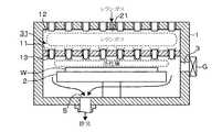
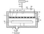
本発明の実施の形態の基板処理装置を成膜装置に適用した一例について、図1〜図3を参照して説明する。この成膜装置は、処理容器1と、この処理容器1内に設けられ、基板である半導体ウエハ(以下「ウエハ」と言う)Wを載置するための載置部である載置台2と、処理容器1の例えば天井面における中央部に形成された処理ガス供給口21から後述の処理ガスを当該処理容器1内に供給するための処理ガス供給路22と、を備えている。処理ガス供給路22には、バルブ23及び流量調整部24を介して、H(水素)の活性種と成膜種である例えばSi(シリコン)とを生成する処理ガス例えばシラン(SiH4)ガスのガス源25が接続されている。この例では、ガス源25から処理ガス供給口21に至るまでの部分がガス供給部に相当する。 An example in which the substrate processing apparatus according to the embodiment of the present invention is applied to a film forming apparatus will be described with reference to FIGS. The film forming apparatus includes a
図1中3はゲートバルブGにより気密に密閉されるウエハWの搬送口、4は排気路である。この排気路4は、処理容器1の床面に形成された排気口5から、圧力調整手段6を介して真空排気手段例えば真空ポンプ7に向かって伸びている。また、図1中8は、処理容器1の外部に設けられた電源部9から供給される電圧により、ウエハWを載置台2側に静電吸着するための静電チャックである。尚、この成膜装置には、搬送口3を介して処理容器1内に進入する外部の搬送アームと載置台2との間においてウエハWの受け渡しを行うために、昇降ピン2aが載置台2内を貫通するように設けられている。図1中2bは、昇降ピン2aを昇降させるための昇降部である。 In FIG. 1,
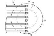
処理容器1の天井面と載置台2との間には、既述の処理ガス供給口21から処理容器1内に供給される処理ガスを拡散させるためのガス拡散板11が載置台2上のウエハWと対向して水平に設けられている。このガス拡散板11には、図2にも示すように、処理容器1の天井面とガス拡散板11との間の領域であるガス拡散空間12に拡散した処理ガスを下方側のウエハWに向けて吐出するためのガス吐出孔(ガス通過孔)13が縦横等間隔に例えば格子状(マトリックス状)に複数形成されている。この図2では、ガス吐出孔13について模式的に示しているが、このガス吐出孔13は、例えば縦横20mm間隔で形成されている。この例では、処理容器1の天井面と側面の一部とガス拡散板11とにより、ガスシャワーヘッドが構成される。 Between the ceiling surface of the
処理容器1の天井面には、図1に示したように、当該天井面から下方側のガス拡散板11に向かって垂直に伸びる概略ロッド状(棒状)の加熱用構造体であるセラミックヒータ31が複数箇所に気密に設けられている。これらのセラミックヒータ31は、図2に示すように、ガス拡散板11を上方側から見た時の投影領域が前記ガス吐出孔13と重なり合うように位置しており、このセラミックヒータ31の下端部(先端部)である後述の加熱部43は、各々のガス吐出孔13内からガス吐出孔13の下方側に亘って位置している。尚、図2には、載置台2上に載置されるウエハWの外縁を点線で示している。 On the ceiling surface of the
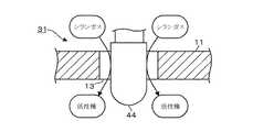
セラミックヒータ31は、セラミック体である中空で棒状のセラミック管33と、このセラミック管33の上端部を間隙を介して被せるようにして設けられた筒状の導電体からなるハウジング32と、を備えている。セラミック管33の材質としては、例えばシリコンナイトライド(SiN)やアルミナ(Al2O3)などが挙げられる。セラミック管33は、先端(下端)がドーム状に閉塞されており、内部には基端部(上端部)側から一対の給電線41、41が長さ方向に配線されている。これら給電線41、41の先端には抵抗発熱体である抵抗発熱線42が設けられている。この抵抗発熱線42はセラミック管33の先端部(下端部)に対応する領域に収められており、給電により発熱することで当該部位が加熱部43として機能する。 The
セラミック管33の上端部である、ハウジング32に囲まれた部位には、大径の接続部45が下方側に、また小径の接続部46が上方側に、互に離間して設けられている。大径の接続部45は、外周面がハウジング32の内周面に密着している。これら接続部45、46はセラミック管33の表面にメタライズ加工がされており、前記一対の給電線41、41の一方及び他方が大径の接続部45及び小径の接続部46に夫々接続されている。従って、一方の給電線41は大径の接続部45を介して一方の電極部をなすハウジング32に電気的に接続されている。また、小径の接続部46からは給電線41が、ハウジング32の上端開口部を塞ぐ絶縁碍子47内を貫通して伸びており、当該給電線41の上端はネジが切られた他方の電極部48に接続されている。このため、一方の電極部(ハウジング)32及び他方の電極部48の間に電力を供給することによって給電線41、41を介して抵抗発熱線42に給電され、この抵抗発熱線42が発熱することになる。ハウジング32及び電極部48は、処理容器1の外方に設けられた電源49に夫々接続されており、既述の抵抗発熱線42に対して例えば50Wの電力を供給し、金属触媒層44を例えば1000℃以上に加熱できるように構成されている。この電源49は、図1に示すように、スイッチ部50を介して既述の複数のセラミックヒータ31に対して直列に接続されている。 At a portion surrounded by the
セラミック管33の外周面における、抵抗発熱線42により予め設定した温度に加熱される領域には、触媒が付着されている。具体的にはセラミック管の先端部の外周面に金属触媒層44が設けられている。この金属触媒層44は、触媒金属例えばW(タングステン)、Ir(イリジウム)、Pt(白金)、Mo(モリブデン)、Ru(ルテニウム)、Pd(パラジウム)、Co(コバルト)、Ni(ニッケル)などの高融点金属が例えばCVD(Chemical Vapor Deposition)法、スパッタ法、PVD(Physical Vapor Deposition)法あるいは無電解メッキ法などにより形成されている。 A catalyst is attached to a region of the outer peripheral surface of the
この金属触媒層44は、当該金属触媒層44の周囲におけるガス吐出孔13を介して上方側から下方側に向かう処理ガスを当該金属触媒層44にできるだけ接触させるために、高さ位置がガス拡散板11と重なり合うように、また上下の端面が夫々ガス拡散板11の上方側及び下方側に突き出るように高さ寸法が設定されている。なお、前記加熱部43は金属触媒層44が形成されていることから、処理ガスの活性化に有効な温度に発熱する部位であるということができる。 The
また、金属触媒層44の下端面と載置台2上のウエハWの表面との間の離間距離hは、金属触媒層44に処理ガスが接触して生成する活性種ができるだけ失活せずに速やかにウエハWに供給されるように、例えば1cmとなっている。前記セラミック管33は、後述の樹脂などからなるO−リング35と抵抗発熱線42により加熱される加熱部43とを離間させて当該O−リング35を高温から保護するために、上端面から加熱部43までの長さ寸法Hが例えば5cmとなっている。 Further, the separation distance h between the lower end surface of the
続いて、セラミックヒータ31を処理容器1の天井部に固定する構造について説明する。このセラミックヒータ31は、上面側が開口するように処理容器1の天井面に固定されたカップ型の絶縁スリーブ34内において、セラミック管33が当該絶縁スリーブ34の中央部を貫通して下方側に伸びるように支持されている。また、セラミックヒータ31は、ハウジング32の下端部に周方向に形成された段部が絶縁スリーブ34の内側の周縁部に保持されるように、当該セラミックヒータ31を絶縁スリーブ34内に挿入されている。従って、セラミックヒータ31は、処理容器1の天井面からいわば吊り下げられた状態で保持されるように構成されている。図3中、35はハウジング32の外周側を囲むように絶縁スリーブ34の上方側に設けられた樹脂などの弾性体からなるシール部材例えばO−リング、36はこのO−リング35の外周側にて処理容器1の上面部に例えば溶接などにより固定された固定部材、37は固定部材36とハウジング32との間におけるO−リング35の上方側に設けられたリング状の絶縁体からなる押圧部材、38は押圧部材37を下方側に押し込むための概略リング状の密閉部材である。そして、絶縁スリーブ34内にセラミックヒータ31を挿入すると共に、ハウジング32と固定部材36との間にO−リング35及び押圧部材37を下方側からこの順番で積層し、固定部材36の外周面と密閉部材38の内周面とが螺合するように密閉部材38を回動させて締め付けることにより、押圧部材37が下方側に移動してO−リング35を押しつぶし、処理容器1内が気密に保たれるように構成されている。 Then, the structure which fixes the
この成膜装置は、装置全体の動作のコントロールを行うためのコンピュータからなる制御部60を備えており、この制御部60は、CPU、プログラム、メモリ(いずれも図示せず)などを備えている。このプログラムには、ウエハWに対して後述の基板処理例えば成膜処理を行うステップ群が記憶されており、前記プログラムは、ハードディスク、コンパクトディスク、光磁気ディスク、メモリカード、フレキシブルディスクなどの記憶媒体61から制御部60内にインストールされる。 The film forming apparatus includes a
次に、前記成膜装置の作用について、図4及び図5を参照して以下に説明する。先ず、図示しない搬送アームにより搬送口3を介してウエハWを処理容器1内に搬入し、昇降ピン2aとの協働作用により載置台2上にウエハWを載置する。そして、ウエハWを載置台2に静電吸着すると共に、搬送口3をゲートバルブGにより気密に閉じて圧力調整手段6を全開にして処理容器1内を真空引きする。次いで、スイッチ部50をオフ状態からオン状態にし、これにより電源49から各々のセラミックヒータ31に対して例えば50Wの電力を供給する。この電力により抵抗発熱線42が発熱し、この熱がセラミック管33を介して金属触媒層44に伝熱して、当該金属触媒層44が例えば1000℃に加熱される。そして、圧力調整手段6の開度を調整して処理容器1内の圧力を例えば133.33Pa(10Torr)に設定すると共に、処理ガス供給口21から処理容器1内に処理ガス例えばシランガスを例えば100sccmで吐出する。ここで、セラミックヒータ31の基端側(上端側)における処理容器1の固定構造部位(ハウジング32)は、この金属触媒層44(加熱部43)から離間しているので、例えば70℃程度の低い温度に保たれる。この温度は、O−リング35の耐熱温度以下であるため、O−リング35の熱劣化が抑えられる。 Next, the operation of the film forming apparatus will be described below with reference to FIGS. First, the wafer W is loaded into the
処理容器1内に供給された処理ガスは、図4に示すように、処理容器1の天井面とガス拡散板11との間の領域であるガス拡散空間12において拡散し、セラミックヒータ31の金属触媒層44が挿入されているガス吐出孔13から下方側に向かって、当該金属触媒層44に接触しながら下降していく。そして、高温に加熱された金属触媒層44に処理ガスが接触すると、図5に示すように、金属触媒層44の触媒作用によってシランガスが加熱分解されて、H(水素)のラジカルなどの活性種と共に成膜種であるSi(シリコン)の活性種が生成する。この成膜種がウエハWの表面に供給されると、Siが当該ウエハW上に堆積して、例えば多結晶シリコン膜が成膜される。 As shown in FIG. 4, the processing gas supplied into the
そして、未反応の活性種、活性種が死活して生じた分子群及び活性化されなかった気体分子は、副生成物などと共に排気口5へと排気されていく。この時、ガス拡散板11のガス吐出孔13内にセラミックヒータ31の加熱部43が位置しているので、ウエハW側からガス拡散板11を見ると、活性種の供給源がガス吐出孔13のレイアウトに応じて散在していることになる。そして、これら供給源から活性種がガス拡散板11とウエハWとの間の処理空間に供給されて拡散し、ウエハWの面内において均一性の高い濃度分布の状態でウエハWの表面に供給され、この結果膜厚及び膜質について均一性の高い多結晶シリコン膜が成膜されることになる。尚、既述の図4においてはセラミックヒータ31を簡略化して記載している。 Then, the unreacted active species, the molecular groups generated by the active species being dead and activated, and the gas molecules that have not been activated are exhausted to the
上述の実施の形態によれば、触媒により処理ガスを活性化して、活性種を用いてウエハWに対して例えば成膜処理を行うにあたり、内部に抵抗発熱線42が設けられたセラミック管33の表面に触媒を付着させたセラミックヒータ31を用いている。従って、金属触媒層44に電流を流して加熱するのではなく、セラミック管33を介して間接的に金属触媒層44を加熱する構成であるから、加熱するための給電部位(抵抗発熱線42)について、例えば従来のワイヤ状の触媒に通電加熱する場合のような熱膨張による撓みが起こらないので、使用環境に基づく劣化による断線や短絡、あるいは熱損傷のおそれがない。 According to the above-described embodiment, when the process gas is activated by the catalyst and, for example, the film formation process is performed on the wafer W using the active species, the
また、セラミックヒータ31を棒状体に形成し、先端部(下端部)が処理ガスの活性化に有効な温度に加熱する加熱部43として構成されているため、基端部側(処理容器1の天井側)については加熱部43よりも低い温度に保つことができ、例えば樹脂やゴム製のシール部材の耐熱温度以下である低温状態とすることができる。従って、特別なシール構造を構築しなくとも例えば樹脂製のシール材であるO−リング35を用いることができるので、セラミックヒータ31を処理容器1に気密に固定することが容易である。
更に、棒状のセラミックヒータ31を処理容器1内で島状に(点在するように)配置しているため、配置レイアウトの自由度が高く、このため装置設計が容易になるし、装置が制作された後においても調整しやすい。Further, the
Furthermore, since the rod-shaped
また、ガス拡散板11のガス吐出孔13に対応して、この例ではガス吐出孔13内にセラミックヒータ31の加熱部43を位置させているので、処理ガスは、散在しているガス吐出孔13の通過時に加熱部43に高い効率で接触する。このため、処理ガスは熱分解して活性化されやすいので、ウエハWと対向している面に形成された多数の活性種源から濃度の高い活性種がウエハWに降り注がれ、ウエハWの面内において均一性の高い成膜処理を実現できる。 Further, in this example, since the
更に、セラミックヒータ31の加熱部43に面状に金属触媒層44を形成しているので、従来のワイヤ状の触媒を設ける場合と比較して、処理容器1内に配置できる金属触媒層44の表面積を広くすることができる。そのため、処理ガスと金属触媒層44との接媒する領域が増加することから、ワイヤ状の触媒を用いる場合よりも処理ガスの活性化により生じる活性種を多く生成することができ、高い成膜速度を得ることができる。また、セラミックヒータ31の表面の金属触媒層44が酸化等で劣化した場合でも、再被覆により再生できる。更にまた、金属触媒層44を加熱部43の表面に形成するにあたって、既述のように金属触媒層44を構成する金属材料のスパッタ法などを用いることができるので、製作コストが低廉である。また、複数のセラミックヒータ31を配置しているので、例えば1つのセラミックヒータ31について金属触媒層44の不具合などが起こったとしても、当該セラミックヒータ31だけを取り外して交換あるいは修理できるので、例えば断線が起こった時には触媒を一式交換する必要のあった従来の例えば蛇腹状あるいは網状のワイヤからなる触媒を設置する場合よりもコストを低減できる。 Furthermore, since the
また、既述の多結晶シリコン膜を形成するにあたって、ウエハWを直接加熱したり、あるいはプラズマを用いたりせずに、金属触媒層44により処理ガスを活性化させているので、これらの方法よりもウエハWに対するダメージを低減できる。
既述の例では、セラミックヒータ31及びガス吐出孔13を格子状に配置したが、例えば同心円状や千鳥状に配置しても良いし、例えばウエハWの中心部側に対して周縁部側においてセラミックヒータ31の配置個数を多くしても良い。また、各々のセラミックヒータ31に対して電源49を直列に接続したが、並列に接続しても良いし、電源49を並列に接続すると共に各々のセラミックヒータ31に対して供給する電力値を調整しても良い。In forming the polycrystalline silicon film described above, the processing gas is activated by the
In the above-described example, the
また、セラミックヒータ31及びガス吐出孔13の配置例としては、例えば図6に示すように、載置台2上のウエハWの直径方向に沿って複数箇所に例えば一列に設けても良い。そして、図7に示すように、載置台2の下方側に当該載置台2を鉛直軸回りに回転させる移動機構70を設けて、成膜処理を行う時はウエハWを周方向に回転させても良い。尚、既述の例に示す成膜装置にこの移動機構70を設けても良い。 Moreover, as an arrangement example of the
前記各例において、金属触媒層44をガス吐出孔13内に挿入するようにしたが、図8に示すように、金属触媒層44をガス拡散板11から上方側に離間させても良いし、セラミックヒータ31の先端部を既述の実施の形態よりも下方側に位置させてウエハWに近接させても良く、例えば図9に示すように、金属触媒層44の上端部だけガス吐出孔13内に位置させるようにしても良い。更にまた、加熱部43全体をガス吐出孔13よりも下方側であって、当該ガス吐出孔13と対向するように(ガス吐出孔13の投影領域に)位置させても良い。また、各々のガス吐出孔13毎にセラミックヒータ31を配置したが、セラミックヒータ31の個数よりもガス吐出孔13の個数を多くしても良いし、セラミックヒータ31をガス拡散板11の上方に離間させる場合にはセラミックヒータ31の個数よりもガス吐出孔13の個数が少なくなるようにしても良い。 In each of the above examples, the
本発明は、ガス拡散板11を設けなくとも良く、例えば棒状のセラミックヒータ31を既述の実施の形態のようにウエハWの上方に多数垂直に設けると共に、セラミックヒータ31間に、例えばセラミックヒータ31の配列に対して千鳥状となるように多数の処理ガス供給路22を処理容器1の天井部から下方に突出させて、且つ下端側の開口部(処理ガス供給口21)が加熱部43よりも上方側に位置するように設け、下端側の開口部から処理ガスを吐出さえて加熱部43で加熱分解されるような構成であっても良い。 In the present invention, the
更に、既述の図6及び図7に示したようにセラミックヒータ31及びガス吐出孔13をウエハWの直径方向に一列に配置してウエハWを周方向に回転させる場合には、図10及び図11に示すように、例えばガス拡散板11の下方位置において処理容器1の側壁からセラミックヒータ31を処理容器1内に挿入しても良い。このような場合には、図12に示すように、セラミックヒータ31の先端側(加熱部43)を例えば下側に向けてL字型に屈曲させても良い。尚、ガス拡散板11の上方にセラミックヒータ31を設けても良い。 Further, as shown in FIGS. 6 and 7, the
更にまた、既述の各例における円形のウエハWに代えて、例えばLCD(Liquid Crystal Display)基板やFPD(Flat Panel Display)基板などの角型の基板Sに対して既述の処理を行う場合には、図1及び図2のようにセラミックヒータ31及びガス吐出孔13を格子状、同心円、千鳥状に配置しても良いし、あるいは図13及び図14に示すように、基板Sの1辺に沿ってセラミックヒータ31及びガス吐出孔13を例えば一列に配置すると共に、これらのガス吐出孔13から活性種が下方側に吐出される領域を基板Sが一端側から他端側にかけて通過するように、基板Sを水平に搬送する例えばボールネジなどが組み合わされた移動機構71を載置台2に設けても良い。即ち、基板(ウエハWや基板Sなど)に対向する領域の全体ではなく局所的にセラミックヒータ31を配置し(詳しくはセラミックヒータ31の先端の加熱部43を配置し)、これら加熱部43群で囲まれる領域に対向する領域に基板の表面全体が位置するように基板を移動させても良い。更に言い換えれば、加熱部43の配置レイアウトに基づく基板の表面への活性種の供給の不均一性を補償するために、載置台2を横方向に移動させるための移動機構を設けても良いということである。 Furthermore, instead of the circular wafer W in each of the above-described examples, for example, the above-described processing is performed on a square substrate S such as an LCD (Liquid Crystal Display) substrate or an FPD (Flat Panel Display) substrate. For example, the
前記各例において、セラミックヒータ31の修理(金属触媒層44の再被覆)を行う場合には、処理容器1からセラミックヒータ31を取り外して例えば別のスパッタ装置などにおいてスパッタ法などにより金属触媒層44の金属材料の成膜を行っても良いし、あるいは処理容器1にセラミックヒータ31を取り付けたまま、既述の処理ガス供給口21から金属触媒層44を構成する金属を含む処理ガス例えばW(CO)6、Ni(PF3)4、Co2(CO)8、Ru3(CO)12を供給し、抵抗発熱線42により加熱部43を加熱して当該加熱部43の表面において前記処理ガスを分解させて、いわばin−situにてCVD法により金属触媒層44を形成しても良い。この場合には、セラミックヒータ31の交換(修理)に要する時間を短縮できるので、装置のダウンタイムを減らすことができる。In each of the above examples, when repairing the ceramic heater 31 (re-coating of the metal catalyst layer 44), the
また、ロッド状のセラミックヒータ31を設けずに、図15及び図16に示すように、例えばガス拡散板11を既述のセラミックスにより構成すると共に、当該ガス拡散板11の内部領域に水平方向に亘って抵抗発熱線42を埋設し、このガス拡散板11の表面及びガス吐出孔13の内壁面に金属触媒層44を形成しても良い。この場合には、ガス拡散板11が熱膨張により処理容器1の内壁に接触して破損しないように、例えば処理容器1の天井面から支持部72により支持される。そして、処理ガスは、図16に示すように、ガス吐出孔13を上方側から下方側に通過する際に、当該ガス吐出孔13の内壁あるいはガス拡散板11の上下面に形成された金属触媒層44に接触して活性化することになる。 Further, without providing the rod-shaped
前記金属触媒層44の下地であるセラミック管33(ガス拡散板11)の材質としては、SiN以外にも、例えばpBN(パイロリティックボロンナイトライド)などであっても良い。また、処理ガスとしては、既述のシランガスに代えて、金属触媒層44によりHの活性種と成膜種とを生成するガス例えばH2ガスやNH3ガスとSiを含むガス例えばSi2H6、SiH2Cl2とを用いても良い。この場合には、金属触媒層44によりH2ガスが活性化されてHラジカルが生成し、このHラジカルによりSiを含むガスが分解されて成膜種が生成する。また、多結晶シリコン膜以外にも、例えば成膜種を含むガスとしてW(タングステン)を含むガス例えばWF6ガスを用いてW膜を成膜しても良い。更に、既述の基板処理装置において行う処理としては、成膜処理以外にも、例えばウエハWの酸化処理や窒化処理あるいはウエハW表面に形成されたフォトレジスト膜のアッシング処理であっても良い。これらの場合に用いられる処理ガスとしては、酸化処理ではO2(酸素)ガスやH2O(水蒸気)ガス、窒化処理ではNH3ガスやN2ガス、アッシング処理ではNH3ガスやH2ガスが用いられ、金属触媒層44を構成する金属としてはこれらの処理ガスや活性種により劣化しにくい金属材料が適宜選定される。The material of the ceramic tube 33 (gas diffusion plate 11) that is the base of the
W ウエハ
1 処理容器
2 載置台
11 ガス拡散板
13 ガス吐出孔
21 処理ガス供給口
31 セラミックヒータ
43 加熱部
44 金属触媒層
49 電源
Claims (9)
Translated fromJapanese基板を載置するための載置部が内部に設けられ、処理雰囲気を形成する処理容器と、
前記処理容器内に処理ガスを供給するガス供給部と、
前記処理ガスを活性化させるための触媒がその表面に付着され、処理容器の内部に位置するセラミック体と、このセラミック体の内部に設けられた抵抗発熱体と、を含む加熱用構造体と、を備えたことを特徴とする基板処理装置。In an apparatus for processing a substrate using activated species obtained by activating a processing gas,
A processing container is provided inside for mounting a substrate, and forms a processing atmosphere; and
A gas supply unit for supplying a processing gas into the processing container;
A heating structure including a ceramic body that is attached to the surface of the catalyst for activating the processing gas and located inside the processing container, and a resistance heating element provided inside the ceramic body, A substrate processing apparatus comprising:
前記加熱部は、前記ガス通過孔に対向しているかまたは当該ガス通過孔の中に位置していることを特徴とする請求項2または3に記載の基板処理装置。Partitioning between the gas supply unit and the atmosphere on which the substrate is placed, and provided with a gas diffusion plate provided so as to face the substrate and formed with a number of gas passage holes;
The substrate processing apparatus according to claim 2, wherein the heating unit faces the gas passage hole or is located in the gas passage hole.
前記加熱用構造体は、このガス拡散板の少なくとも一部を構成し、
前記加熱用構造体において処理ガスの活性化に有効な温度に加熱する加熱部は、前記ガス拡散板におけるガス通過孔を囲む部分を含むことを特徴とする請求項1に記載の基板処理装置。Partitioning between the gas supply unit and the atmosphere on which the substrate is placed, and provided with a gas diffusion plate provided so as to face the substrate and formed with a number of gas passage holes;
The heating structure constitutes at least a part of the gas diffusion plate,
The substrate processing apparatus according to claim 1, wherein the heating unit that heats the heating structure to a temperature effective for activating the processing gas includes a portion surrounding the gas passage hole in the gas diffusion plate.
Priority Applications (4)
| Application Number | Priority Date | Filing Date | Title |
|---|---|---|---|
| JP2010006270AJP5434614B2 (en) | 2010-01-14 | 2010-01-14 | Substrate processing equipment |
| PCT/JP2011/050425WO2011087049A1 (en) | 2010-01-14 | 2011-01-13 | Substrate processing apparatus |
| KR1020127021273AKR20120112793A (en) | 2010-01-14 | 2011-01-13 | Substrate processing apparatus |
| US13/547,689US8419856B2 (en) | 2010-01-14 | 2012-07-12 | Substrate processing apparatus |
Applications Claiming Priority (1)
| Application Number | Priority Date | Filing Date | Title |
|---|---|---|---|
| JP2010006270AJP5434614B2 (en) | 2010-01-14 | 2010-01-14 | Substrate processing equipment |
Publications (2)
| Publication Number | Publication Date |
|---|---|
| JP2011146543Atrue JP2011146543A (en) | 2011-07-28 |
| JP5434614B2 JP5434614B2 (en) | 2014-03-05 |
Family
ID=44304320
Family Applications (1)
| Application Number | Title | Priority Date | Filing Date |
|---|---|---|---|
| JP2010006270AExpired - Fee RelatedJP5434614B2 (en) | 2010-01-14 | 2010-01-14 | Substrate processing equipment |
Country Status (4)
| Country | Link |
|---|---|
| US (1) | US8419856B2 (en) |
| JP (1) | JP5434614B2 (en) |
| KR (1) | KR20120112793A (en) |
| WO (1) | WO2011087049A1 (en) |
Families Citing this family (1)
| Publication number | Priority date | Publication date | Assignee | Title |
|---|---|---|---|---|
| CN205177785U (en)* | 2013-03-14 | 2016-04-20 | 应用材料公司 | Handle cavity and be used for being coupled to hot line source device of this processing cavity |
Citations (7)
| Publication number | Priority date | Publication date | Assignee | Title |
|---|---|---|---|---|
| JPS6340314A (en)* | 1986-08-05 | 1988-02-20 | Hiroshima Univ | Manufacture of thin film by catalytic cvd method and device therefor |
| JPS63186875A (en)* | 1987-01-29 | 1988-08-02 | Tadahiro Omi | Surface reaction film forming device |
| JP2000150498A (en)* | 1998-11-05 | 2000-05-30 | Nec Corp | Chemical vapor phase growth device and thin film forming method |
| JP2000294535A (en)* | 1999-04-08 | 2000-10-20 | Sony Corp | Vapor phase processing method and its apparatus |
| JP2003041365A (en)* | 2001-07-31 | 2003-02-13 | Hitachi Kokusai Electric Inc | Substrate processing equipment |
| JP2004031701A (en)* | 2002-06-26 | 2004-01-29 | Kyocera Corp | Cat-PECVD method, film formed using the same, thin film device provided with the film, and film processing system |
| JP2009203546A (en)* | 2008-01-29 | 2009-09-10 | Nagaoka Univ Of Technology | Deposition apparatus and deposition method |
Family Cites Families (14)
| Publication number | Priority date | Publication date | Assignee | Title |
|---|---|---|---|---|
| JPH0631178A (en) | 1992-07-14 | 1994-02-08 | Toyota Motor Corp | Resistance heating type catalytic device |
| TW228566B (en)* | 1993-04-02 | 1994-08-21 | Matsushita Refrigeration | Deodorizing device for air conditioner |
| JP3453214B2 (en) | 1995-03-15 | 2003-10-06 | 科学技術振興事業団 | Method of manufacturing thin film transistor by catalytic CVD method and thin film transistor |
| JPH0932536A (en) | 1995-07-17 | 1997-02-04 | Toyota Motor Corp | Electrode structure of electrically heated catalyst and method for forming insulating coating on electrode support holder |
| JPH09106883A (en) | 1996-08-29 | 1997-04-22 | Sharp Corp | Ceramic heater manufacturing method |
| JPH1167727A (en) | 1997-08-19 | 1999-03-09 | Hitachi Ltd | Plasma processing apparatus and method |
| EP1129990A1 (en)* | 2000-02-25 | 2001-09-05 | Lucent Technologies Inc. | Process for controlled growth of carbon nanotubes |
| JP2001358077A (en) | 2000-06-13 | 2001-12-26 | Sharp Corp | Thin film production equipment |
| JP3787816B2 (en) | 2002-10-04 | 2006-06-21 | キヤノンアネルバ株式会社 | Heating element CVD equipment |
| JP4366483B2 (en) | 2004-02-26 | 2009-11-18 | カシオ計算機株式会社 | Reactor |
| US20050188617A1 (en) | 2004-02-26 | 2005-09-01 | Casio Computer Co., Ltd. | Reactor and power generator |
| US7419702B2 (en)* | 2004-03-31 | 2008-09-02 | Tokyo Electron Limited | Method for processing a substrate |
| WO2006093589A2 (en)* | 2005-02-25 | 2006-09-08 | O.I. Corporation | Improved analyte system |
| JP3887690B2 (en) | 2005-12-26 | 2007-02-28 | キヤノンアネルバ株式会社 | Connection structure between heating element and power supply mechanism in heating element CVD device |
- 2010
- 2010-01-14JPJP2010006270Apatent/JP5434614B2/ennot_activeExpired - Fee Related
- 2011
- 2011-01-13KRKR1020127021273Apatent/KR20120112793A/ennot_activeAbandoned
- 2011-01-13WOPCT/JP2011/050425patent/WO2011087049A1/enactiveApplication Filing
- 2012
- 2012-07-12USUS13/547,689patent/US8419856B2/ennot_activeExpired - Fee Related
Patent Citations (7)
| Publication number | Priority date | Publication date | Assignee | Title |
|---|---|---|---|---|
| JPS6340314A (en)* | 1986-08-05 | 1988-02-20 | Hiroshima Univ | Manufacture of thin film by catalytic cvd method and device therefor |
| JPS63186875A (en)* | 1987-01-29 | 1988-08-02 | Tadahiro Omi | Surface reaction film forming device |
| JP2000150498A (en)* | 1998-11-05 | 2000-05-30 | Nec Corp | Chemical vapor phase growth device and thin film forming method |
| JP2000294535A (en)* | 1999-04-08 | 2000-10-20 | Sony Corp | Vapor phase processing method and its apparatus |
| JP2003041365A (en)* | 2001-07-31 | 2003-02-13 | Hitachi Kokusai Electric Inc | Substrate processing equipment |
| JP2004031701A (en)* | 2002-06-26 | 2004-01-29 | Kyocera Corp | Cat-PECVD method, film formed using the same, thin film device provided with the film, and film processing system |
| JP2009203546A (en)* | 2008-01-29 | 2009-09-10 | Nagaoka Univ Of Technology | Deposition apparatus and deposition method |
Also Published As
| Publication number | Publication date |
|---|---|
| JP5434614B2 (en) | 2014-03-05 |
| US8419856B2 (en) | 2013-04-16 |
| US20120279452A1 (en) | 2012-11-08 |
| WO2011087049A1 (en) | 2011-07-21 |
| KR20120112793A (en) | 2012-10-11 |
Similar Documents
| Publication | Publication Date | Title |
|---|---|---|
| TWI708315B (en) | High temperature substrate pedestal module and components thereof | |
| CN106148915B (en) | Substrate pedestal module including backside gas delivery line and method of making the same | |
| TWI390075B (en) | Touch chemical chemical vaporization device | |
| JP3780364B2 (en) | Heating element CVD equipment | |
| KR102213395B1 (en) | Electrostatic chuck mechanism and semiconductor processing device | |
| JP5135710B2 (en) | Film forming method and film forming apparatus | |
| KR101579503B1 (en) | Substrate processing apparatus, method of manufacturing semiconductor device and non-transitory computer readable recording medium | |
| JP2011165891A (en) | Mounting stand structure, and processing device | |
| WO2004090960A1 (en) | Loading table and heat treating apparatus having the loading table | |
| WO2005041285A1 (en) | Shower head and film-forming device using the same | |
| CN109314055A (en) | Atomic layer growth apparatus and atomic layer growth method | |
| JP4435111B2 (en) | ALD apparatus and method for manufacturing semiconductor device | |
| KR20110025101A (en) | Mounting structure and processing unit | |
| JP2004128322A (en) | Heating element CVD apparatus and connection structure between heating element and power supply mechanism in heating element CVD apparatus | |
| KR20020000723A (en) | Single-substrate-processing apparatus for semiconductor process | |
| JP2009076598A (en) | Mounting stand structure and treatment equipment | |
| JP5434614B2 (en) | Substrate processing equipment | |
| JP2010103544A (en) | Film forming apparatus and method | |
| TW200834688A (en) | Prevention of film deposition on PECVD process chamber wall | |
| JP2007327097A (en) | Plasma treatment apparatus | |
| JP4384645B2 (en) | Processing tube | |
| JP2003213421A (en) | Substrate processing equipment | |
| TW202342806A (en) | Showerhead assembly with heated showerhead | |
| JP5903666B2 (en) | Film forming apparatus and film forming method using the same | |
| TWI618112B (en) | Apparatus for coupling a hot wire source to a process chamber |
Legal Events
| Date | Code | Title | Description |
|---|---|---|---|
| A621 | Written request for application examination | Free format text:JAPANESE INTERMEDIATE CODE: A621 Effective date:20120822 | |
| TRDD | Decision of grant or rejection written | ||
| A01 | Written decision to grant a patent or to grant a registration (utility model) | Free format text:JAPANESE INTERMEDIATE CODE: A01 Effective date:20131112 | |
| A61 | First payment of annual fees (during grant procedure) | Free format text:JAPANESE INTERMEDIATE CODE: A61 Effective date:20131125 | |
| R150 | Certificate of patent or registration of utility model | Ref document number:5434614 Country of ref document:JP Free format text:JAPANESE INTERMEDIATE CODE: R150 Free format text:JAPANESE INTERMEDIATE CODE: R150 | |
| R250 | Receipt of annual fees | Free format text:JAPANESE INTERMEDIATE CODE: R250 | |
| R250 | Receipt of annual fees | Free format text:JAPANESE INTERMEDIATE CODE: R250 | |
| R250 | Receipt of annual fees | Free format text:JAPANESE INTERMEDIATE CODE: R250 | |
| R250 | Receipt of annual fees | Free format text:JAPANESE INTERMEDIATE CODE: R250 | |
| LAPS | Cancellation because of no payment of annual fees |