JP2011146447A - Imprint apparatus and article manufacturing method - Google Patents
Imprint apparatus and article manufacturing methodDownload PDFInfo
- Publication number
- JP2011146447A JP2011146447AJP2010004445AJP2010004445AJP2011146447AJP 2011146447 AJP2011146447 AJP 2011146447AJP 2010004445 AJP2010004445 AJP 2010004445AJP 2010004445 AJP2010004445 AJP 2010004445AJP 2011146447 AJP2011146447 AJP 2011146447A
- Authority
- JP
- Japan
- Prior art keywords
- mold
- substrate
- release force
- shot
- imprint
- Prior art date
- Legal status (The legal status is an assumption and is not a legal conclusion. Google has not performed a legal analysis and makes no representation as to the accuracy of the status listed.)
- Withdrawn
Links
Images


Classifications
- B—PERFORMING OPERATIONS; TRANSPORTING
- B29—WORKING OF PLASTICS; WORKING OF SUBSTANCES IN A PLASTIC STATE IN GENERAL
- B29C—SHAPING OR JOINING OF PLASTICS; SHAPING OF MATERIAL IN A PLASTIC STATE, NOT OTHERWISE PROVIDED FOR; AFTER-TREATMENT OF THE SHAPED PRODUCTS, e.g. REPAIRING
- B29C43/00—Compression moulding, i.e. applying external pressure to flow the moulding material; Apparatus therefor
- B29C43/02—Compression moulding, i.e. applying external pressure to flow the moulding material; Apparatus therefor of articles of definite length, i.e. discrete articles
- B29C43/021—Compression moulding, i.e. applying external pressure to flow the moulding material; Apparatus therefor of articles of definite length, i.e. discrete articles characterised by the shape of the surface
- B—PERFORMING OPERATIONS; TRANSPORTING
- B29—WORKING OF PLASTICS; WORKING OF SUBSTANCES IN A PLASTIC STATE IN GENERAL
- B29C—SHAPING OR JOINING OF PLASTICS; SHAPING OF MATERIAL IN A PLASTIC STATE, NOT OTHERWISE PROVIDED FOR; AFTER-TREATMENT OF THE SHAPED PRODUCTS, e.g. REPAIRING
- B29C33/00—Moulds or cores; Details thereof or accessories therefor
- B29C33/56—Coatings, e.g. enameled or galvanised; Releasing, lubricating or separating agents
- B29C33/58—Applying the releasing agents
- B—PERFORMING OPERATIONS; TRANSPORTING
- B29—WORKING OF PLASTICS; WORKING OF SUBSTANCES IN A PLASTIC STATE IN GENERAL
- B29C—SHAPING OR JOINING OF PLASTICS; SHAPING OF MATERIAL IN A PLASTIC STATE, NOT OTHERWISE PROVIDED FOR; AFTER-TREATMENT OF THE SHAPED PRODUCTS, e.g. REPAIRING
- B29C43/00—Compression moulding, i.e. applying external pressure to flow the moulding material; Apparatus therefor
- B29C43/32—Component parts, details or accessories; Auxiliary operations
- B29C43/50—Removing moulded articles
- B—PERFORMING OPERATIONS; TRANSPORTING
- B29—WORKING OF PLASTICS; WORKING OF SUBSTANCES IN A PLASTIC STATE IN GENERAL
- B29C—SHAPING OR JOINING OF PLASTICS; SHAPING OF MATERIAL IN A PLASTIC STATE, NOT OTHERWISE PROVIDED FOR; AFTER-TREATMENT OF THE SHAPED PRODUCTS, e.g. REPAIRING
- B29C43/00—Compression moulding, i.e. applying external pressure to flow the moulding material; Apparatus therefor
- B29C43/32—Component parts, details or accessories; Auxiliary operations
- B29C43/58—Measuring, controlling or regulating
- B—PERFORMING OPERATIONS; TRANSPORTING
- B29—WORKING OF PLASTICS; WORKING OF SUBSTANCES IN A PLASTIC STATE IN GENERAL
- B29C—SHAPING OR JOINING OF PLASTICS; SHAPING OF MATERIAL IN A PLASTIC STATE, NOT OTHERWISE PROVIDED FOR; AFTER-TREATMENT OF THE SHAPED PRODUCTS, e.g. REPAIRING
- B29C43/00—Compression moulding, i.e. applying external pressure to flow the moulding material; Apparatus therefor
- B29C43/02—Compression moulding, i.e. applying external pressure to flow the moulding material; Apparatus therefor of articles of definite length, i.e. discrete articles
- B29C43/021—Compression moulding, i.e. applying external pressure to flow the moulding material; Apparatus therefor of articles of definite length, i.e. discrete articles characterised by the shape of the surface
- B29C2043/023—Compression moulding, i.e. applying external pressure to flow the moulding material; Apparatus therefor of articles of definite length, i.e. discrete articles characterised by the shape of the surface having a plurality of grooves
- B29C2043/025—Compression moulding, i.e. applying external pressure to flow the moulding material; Apparatus therefor of articles of definite length, i.e. discrete articles characterised by the shape of the surface having a plurality of grooves forming a microstructure, i.e. fine patterning
- B—PERFORMING OPERATIONS; TRANSPORTING
- B29—WORKING OF PLASTICS; WORKING OF SUBSTANCES IN A PLASTIC STATE IN GENERAL
- B29C—SHAPING OR JOINING OF PLASTICS; SHAPING OF MATERIAL IN A PLASTIC STATE, NOT OTHERWISE PROVIDED FOR; AFTER-TREATMENT OF THE SHAPED PRODUCTS, e.g. REPAIRING
- B29C43/00—Compression moulding, i.e. applying external pressure to flow the moulding material; Apparatus therefor
- B29C43/32—Component parts, details or accessories; Auxiliary operations
- B29C43/58—Measuring, controlling or regulating
- B29C2043/5808—Measuring, controlling or regulating pressure or compressing force
- B—PERFORMING OPERATIONS; TRANSPORTING
- B29—WORKING OF PLASTICS; WORKING OF SUBSTANCES IN A PLASTIC STATE IN GENERAL
- B29C—SHAPING OR JOINING OF PLASTICS; SHAPING OF MATERIAL IN A PLASTIC STATE, NOT OTHERWISE PROVIDED FOR; AFTER-TREATMENT OF THE SHAPED PRODUCTS, e.g. REPAIRING
- B29C43/00—Compression moulding, i.e. applying external pressure to flow the moulding material; Apparatus therefor
- B29C43/32—Component parts, details or accessories; Auxiliary operations
- B29C43/58—Measuring, controlling or regulating
- B29C2043/5833—Measuring, controlling or regulating movement of moulds or mould parts, e.g. opening or closing, actuating
- B—PERFORMING OPERATIONS; TRANSPORTING
- B29—WORKING OF PLASTICS; WORKING OF SUBSTANCES IN A PLASTIC STATE IN GENERAL
- B29C—SHAPING OR JOINING OF PLASTICS; SHAPING OF MATERIAL IN A PLASTIC STATE, NOT OTHERWISE PROVIDED FOR; AFTER-TREATMENT OF THE SHAPED PRODUCTS, e.g. REPAIRING
- B29C43/00—Compression moulding, i.e. applying external pressure to flow the moulding material; Apparatus therefor
- B29C43/32—Component parts, details or accessories; Auxiliary operations
- B29C43/58—Measuring, controlling or regulating
- B29C2043/5866—Measuring, controlling or regulating ejection of moulded articles
- H—ELECTRICITY
- H01—ELECTRIC ELEMENTS
- H01L—SEMICONDUCTOR DEVICES NOT COVERED BY CLASS H10
- H01L21/00—Processes or apparatus adapted for the manufacture or treatment of semiconductor or solid state devices or of parts thereof
- H01L21/02—Manufacture or treatment of semiconductor devices or of parts thereof
- H01L21/04—Manufacture or treatment of semiconductor devices or of parts thereof the devices having potential barriers, e.g. a PN junction, depletion layer or carrier concentration layer
- H01L21/50—Assembly of semiconductor devices using processes or apparatus not provided for in a single one of the groups H01L21/18 - H01L21/326 or H10D48/04 - H10D48/07 e.g. sealing of a cap to a base of a container
- H01L21/56—Encapsulations, e.g. encapsulation layers, coatings
- H01L21/565—Moulds
- H—ELECTRICITY
- H01—ELECTRIC ELEMENTS
- H01L—SEMICONDUCTOR DEVICES NOT COVERED BY CLASS H10
- H01L2924/00—Indexing scheme for arrangements or methods for connecting or disconnecting semiconductor or solid-state bodies as covered by H01L24/00
- H01L2924/0001—Technical content checked by a classifier
- H01L2924/0002—Not covered by any one of groups H01L24/00, H01L24/00 and H01L2224/00
Landscapes
- Engineering & Computer Science (AREA)
- Mechanical Engineering (AREA)
- Shaping Of Tube Ends By Bending Or Straightening (AREA)
- Exposure Of Semiconductors, Excluding Electron Or Ion Beam Exposure (AREA)
Abstract
Translated fromJapaneseDescription
Translated fromJapanese本発明は、原版となる型のパターンをウエハ等の基板へ転写するインプリント装置及びインプリント装置を使用する物品の製造方法に関する。 The present invention relates to an imprint apparatus for transferring a pattern of a mold as an original to a substrate such as a wafer, and a method for manufacturing an article using the imprint apparatus.
紫外線やX線、あるいは、電子ビームによるフォトリソグラフィーを用いた半導体デバイスへの微細パターンの形成方法に代わる技術としてインプリントが既に知られている。インプリントは、電子ビーム露光等によって、微細なパターンを形成した型(モールド)を、樹脂材料を塗布したウエハ等の基板に押し付ける(押印する)ことによって、樹脂上にパターンを転写する技術である。インプリントには幾つかの種類があり、その一方法として光硬化法が従来から提案されている(例えば、特許文献1を参照のこと)。光硬化法は、基板に塗布された樹脂に透明な型を押し付けた状態で紫外線を出射して樹脂を硬化させ、硬化した樹脂から型を引き離す(離型する)。この光硬化法によるインプリントは、温度制御が比較的容易に行える点や透明な型越しに基板上のアライメントマークの観察が出来る点から半導体集積回路の製造に適している。また、異なるパターンの重ね合せを考慮すると、製造するデバイスのチップの大きさに合せた型を製作し、基板上のショットに逐次転写するステップ・アンド・リピート方式の適用が好ましい。 Imprinting is already known as an alternative technique for forming a fine pattern on a semiconductor device using photolithography using ultraviolet rays, X-rays, or an electron beam. Imprint is a technique for transferring a pattern onto a resin by pressing (imprinting) a mold (mold) on which a fine pattern has been formed by electron beam exposure or the like against a substrate such as a wafer coated with a resin material. . There are several types of imprints, and a photocuring method has been proposed as one of the methods (see, for example, Patent Document 1). In the photocuring method, ultraviolet rays are emitted in a state where a transparent mold is pressed against the resin applied to the substrate to cure the resin, and the mold is separated (released) from the cured resin. This imprinting by the photocuring method is suitable for the manufacture of a semiconductor integrated circuit from the point that the temperature can be controlled relatively easily and the alignment mark on the substrate can be observed through a transparent mold. In consideration of superposition of different patterns, it is preferable to apply a step-and-repeat method in which a mold matching the size of a chip of a device to be manufactured is manufactured and transferred sequentially to shots on a substrate.
一般に、インプリントでは、硬化した樹脂から型を引き離す離型が課題とされている。離型性が低い状態で無理に樹脂から型を引き離すと型が損傷したりして、インプリント装置の耐久性が低下することがある。特許文献2には、離型力を検出し、検出した離型力を閾値と比較して異常の有無を判断し、異常があると判断する場合に、型を加熱する等して離型性を向上させる異常収拾処理を行うことが開示されている。 In general, in imprinting, it is a problem to release a mold from a cured resin. If the mold is forcibly separated from the resin in a state where the releasability is low, the mold may be damaged, and the durability of the imprint apparatus may be lowered. In
型の離型性が低下すると、型の離型時に樹脂に形成されたパターンが崩壊したり型の凹部に目詰まりが発生したりすることがあった。これらの事態の発生を回避するために、インプリント動作を規定回数実施した後に型を回収し、型の洗浄と型に対する離型剤の再塗布を行う必要があった。型の回収、洗浄、離型剤の再塗布のための手間と時間を考えると、型をより長く使用したいが、インプリントの条件によっては、規定回数に達しなくても上述した問題が発生することがあり、型を交換する適正なタイミングを決定することが困難であった。 When the mold releasability is lowered, the pattern formed on the resin may be collapsed at the time of mold release or clogging may occur in the concave portion of the mold. In order to avoid the occurrence of these situations, it has been necessary to collect the mold after performing the imprint operation a specified number of times, and to wash the mold and re-apply the release agent to the mold. Considering the time and effort for mold recovery, cleaning, and re-application of mold release agent, I want to use the mold longer, but depending on imprint conditions, the above-mentioned problems occur even if the number of times is not reached In some cases, it was difficult to determine the proper timing for changing the mold.
そこで、本発明は、型を交換するタイミングを適正化したインプリント装置を提供することを例示的目的とする。 Accordingly, an object of the present invention is to provide an imprint apparatus in which the timing for exchanging molds is optimized.
本発明は、基板に樹脂を塗布し、前記塗布された樹脂に型を押し付けた状態で前記樹脂を硬化させるインプリント動作を前記基板のショット毎に行うインプリント装置であって、型を支持する支持体と、基板を支持する基板ステージと、前記型に加えられた力を検出する検出器と、前記支持体と前記基板ステージとの間に前記支持体に支持された前記型を取り外すための空間を作り出す機構と、制御部と、を備え、前記制御部は、硬化した樹脂から前記型を引き離すために要する離型力を前記検出器の検出結果に基づいて決定し、前記決定された離型力を第1の閾値と比較し、前記決定された離型力が前記第1の閾値より大きいならば前記機構に前記空間を作り出させる、ことを特徴とする。 The present invention is an imprint apparatus that performs an imprint operation for applying a resin to a substrate and curing the resin in a state in which the mold is pressed against the applied resin for each shot of the substrate, and supports the mold A support, a substrate stage that supports the substrate, a detector that detects a force applied to the mold, and the mold supported by the support between the support and the substrate stage are removed. A mechanism for creating a space; and a control unit, wherein the control unit determines a release force required to separate the mold from the cured resin based on a detection result of the detector, and determines the determined release The mold force is compared with a first threshold value, and if the determined release force is greater than the first threshold value, the mechanism creates the space.
本発明によれば、型を交換するタイミングを適正化したインプリント装置を提供することができる。 ADVANTAGE OF THE INVENTION According to this invention, the imprint apparatus which optimized the timing which replace | exchanges a type | mold can be provided.
以下、添付図面を参照して、本発明に係る光硬化法のインプリント装置について説明する。 Hereinafter, an imprint apparatus of a photocuring method according to the present invention will be described with reference to the accompanying drawings.
[実施例1]
図1は、インプリント装置の構成図で、図2は、インプリント装置の制御ブロック図である。インプリント装置は、基板に樹脂を塗布し、塗布された樹脂に型を押し付けた状態で樹脂を硬化させるインプリント動作を基板のショット毎に行う。[Example 1]
FIG. 1 is a configuration diagram of the imprint apparatus, and FIG. 2 is a control block diagram of the imprint apparatus. The imprint apparatus performs an imprint operation for applying a resin to a substrate and curing the resin in a state where a mold is pressed against the applied resin for each shot of the substrate.
図1及び図2において、ウエハ等の基板1は、基板チャック2によって保持される。微動ステージ3は、基板1のθ(z軸回りの回転)方向位置の補正機能、基板1のz位置の調整機能、及び基板1の傾きを補正するためのチルト機能を有する。微動ステージ3は、基板1を所定の位置に位置決めするためのXYステージ4上に配置される。微動ステージ3とXYステージ4とを合せて、基板1を支持する基板ステージと総称する。XYステージ4は、ベース定盤5に載置される。参照ミラー6は、微動ステージ3上のx方向及びy方向(y方向の参照ミラーは不図示)に取り付けられ、微動ステージ3の位置を計測するためにレーザ干渉計7からの光を反射する。支柱8,8'は、ベース定盤5上に屹立し、天板9を支える。型(モールド)10は、図示しない機械的保持機構によって、型チャック11に固定される。型チャック11は、型10を支持する支持体を構成する。型10の表面には、基板1に転写されるべき凹凸のパターンが形成されている。型チャック11は、同じく図示しない機械的保持機構によって、型チャックステージ12に載置される。 1 and 2, a
型チャックステージ12は、型10(又は型チャック11)のz軸回りの回転(θ)方向位置の補正機能及び型10の傾きを補正するためのチルト機能を有する。型チャック11は、そのx方向及びy方向の位置を計測するためにレーザ干渉計7'からの光を反射する反射面を有する(y方向の反射面は不図示)。型チャック11及び型チャックステージ12には、光源16からコリメータレンズ17を通して出射される紫外光を型10へと通過させる、図示しない開口をそれぞれ有する。ガイドバープレート13は、その一端が型チャックステージ12に固定され、天板9を貫通するガイドバー14,14'の他端を固定する。 The
型昇降用のリニアアクチュエータ15,15'は、エアシリンダ又はリニアモータからなり、ガイドバー14,14'を図1のz方向に駆動し、型チャック11に保持された型10を基板1に押し付けたり、引き離したりする。リニアアクチュエータ15,15'は、型10を支持する支持体を駆動する駆動機構を構成する。リニアアクチュエータ15,15'は、また、型を支持する支持体と基板ステージ3,4との間に、支持体に支持された型10を取り外すための空間を作り出す機構を構成している。なお、空間を作り出す機構は、リニアアクチュエータ15,15'ではなく、基板ステージ3,4を駆動する駆動機構としてもよい。天板9に支柱19及び19'により懸架されたアライメント棚18には、ガイドバー14及び14'が貫通している。静電容量センサ等のギャップセンサ20は、基板チャック2上の基板1の高さ(平坦度)を計測する。 The
複数のロードセル21(図1に図示せず)は、型チャック11又は型チャックステージ12に取り付けられ、型10を基板1に押し付ける場合と基板1から引き離す場合において型10に加えられた力を計測する検出器である。なお、型10に加えられた力を計測する検出器は、型10に取り付けられた歪みゲージであってもよい。 A plurality of load cells 21 (not shown in FIG. 1) are attached to the
ダイバイダイアライメント用のTTM(スルー・ザ・モールド)アライメントスコープ30,30'は、基板1と型10とに設けられたアライメントマークを観察するための光学系と撮像系とを有する。TTMアライメントスコープ30,30'は、基板1と型10のx方向及びy方向の位置ずれを計測する。ディスペンサヘッド32は、基板1の表面に液状の光硬化性の樹脂を滴下する樹脂滴下ノズルを備えている。微動ステージ3上に配置された基準マーク台上には、基準マーク50が配置されている。CPU(制御部)100は、以上のアクチュエータやセンサ類を統括して、インプリント装置に所定の動作をさせる。メモリ(記憶部)110には、インプリント動作を実行するときの離型力の推移を含む、型10の転写履歴や、型交換時期の判定に必要な離型力に関するデータが記憶されている。表示部120は、後述するように、型10の交換をうながすメッセージや樹脂の充填不良の発生を表示する。 The die-by-die alignment TTM (through-the-mold)
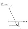
ここで図1から図5を用いて、半導体デバイス作成時のインプリント装置の動きについて説明する。図3は、ロードセル21により計測される、離型時において型10に加えられた力の時間変化の一例を示したグラフである。図3において、マイナス側に働く力の最大値の絶対値を離型力FLと呼ぶ。 Here, the operation of the imprint apparatus when creating a semiconductor device will be described with reference to FIGS. FIG. 3 is a graph showing an example of the time change of the force applied to the
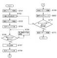
図4は、複数枚の基板1に同じ型10を使用してインプリント動作を実行する実施例1のフローチャートである。S101で、CPU100は、メモリ110に保存されている型毎の転写履歴から、使用する型の基準離型力F0を確認する。基準離型力F0は、使用する基板1や下地、型10、離型剤、樹脂、型の押し付け荷重、型の押し付け時間、紫外線の照射時間、離型時の型の引き離し速度といった条件で事前にインプリントを行って得られた離型力である。この事前のインプリントでは、基板上の全てのショットでインプリントを行う必要はない。例えば図6に示すショット配置で、基板中心付近の複数ショットでインプリントを行い、その結果得られた離型力の平均値もしくは最大値を基準離型力F0として、メモリ110に保存しておく。また、型10の洗浄や離型剤の塗布を行った場合、同様の事前のインプリントを行って基準離型力F0の値を更新する。 FIG. 4 is a flowchart of the first embodiment in which an imprint operation is performed using the
次に、S1で、図示しない型搬送機構が、型10を型チャック11に供給する。S2で、TTMアライメントスコープ30、30'により型10の図示しないアライメントマークと微動ステージ3上の基準マーク50とを同時に観察する。そして、この観察結果を使用して、型チャックステージ12により主に型10のθ(z軸回りの回転)方向の位置を合せる。次に、S3で、図示しない基板搬送機構が、基板1を基板チャック2に供給する。続くS4で、CPU100は、XYステージ4を駆動して、ギャップセンサ20により基板1全面の高さ(平坦度)を計測する。この計測データは後述するように、型10の押印時に、基板1のインプリント動作を行うショット面を基準平面に合せる際に使用される。 Next, a mold transport mechanism (not shown) supplies the
S5で、プリアライメント計測器(図示せず)により、基板1上に先行して形成されたプリアライメントマーク(図示せず)を撮像し観察する。そして、画像処理により基板1のインプリント装置に対するx方向とy方向のずれを計測し、その結果を元に基板1のθ(z軸回りの回転)方向の位置補正を行う。S6で、TTMアライメントスコープ30、30'を使用して、基板1上の特定のサンプルショット(図示せず)において、型10上のアライメントマーク(図示せず)と基板1上のアライメントマーク(図示せず)を同時に観察する。そして、x方向とy方向の相対的位置ずれ量を計測する。これらのx方向及びy方向の位置ずれからθ(z軸回りの回転)方向の位置ずれも算出される。サンプルショットでのTTMアライメントスコープによる計測結果から、基板1上の各ショットにおけるx方向、y方向、θ方向のずれを予測して、ショットごとの転写を行う際の基板ステージの位置合せ目標位置が決定される。この手法は、ステップ・アンド・リピート方式の露光装置で用いられているグローバルアライメント計測の手法と同じである。 In S5, a pre-alignment measuring instrument (not shown) images and observes a pre-alignment mark (not shown) formed on the
S7で、基板1上の各ショットに対して、図5に示すフローチャートによるインプリント動作が行われる。全ショットに対するインプリント動作が終了すると、S8で、図示しない基板搬送機構により基板1が基板チャック2から回収される。S9で、CPU100は、続いてインプリントする基板があるか否か判定し、次にインプリントする基板がある場合は、インプリント動作が可能なショット数と次の基板でインプリントするショット数とを比較する。続いてインプリントする基板があり、インプリント動作が可能なショット数が次の基板のインプリントするショット数より大きい場合はS3に戻る。次にインプリントする基板が無い場合、又は、後述するようにS7で型交換を行うことになった場合はS10に進む。最後に、S10で、図示しない型搬送機構により型チャック11から型10の回収を行って、複数の基板に対するインプリントを終了する。 In S7, an imprint operation according to the flowchart shown in FIG. 5 is performed for each shot on the
図5は、一枚の基板に対するインプリント動作のフローチャートで、図4のS7に相当する。以下、図5と図1、図2を用いて、インプリント動作について説明する。図5において、S701で、CPU100は、XYステージ4を駆動し、基板1の載置された基板チャック2を移動させ、基板1上のインプリントを行うショットをディスペンサヘッド32の下に移動させる。S702で、ディスペンサヘッド32によって基板1上の対象とするショットに光硬化樹脂を滴下する。S703で、CPU100は、該当ショットの平面が型10の凹凸パターンと対向する位置に来るようにXYステージ4を駆動する。この際、基板ステージは図3のS6のアライメント計測の結果によって決定され補正された位置合せ目標位置に移動する。さらに、微動ステージ3により基板チャック2のz方向の高さと傾きを調整して、前述の基板高さ計測データを元にして、基板1の該当ショットの表面を基準平面に合せる。そして、S704で、CPU100は、リニアアクチュエータ15,15'を駆動することにより型チャック11を所定位置まで下降させる。 FIG. 5 is a flowchart of the imprint operation for one substrate, and corresponds to S7 in FIG. Hereinafter, the imprint operation will be described with reference to FIGS. 5, 1, and 2. In FIG. 5, in step S <b> 701, the
S705で、CPU100は、型チャック11又は型チャックステージ12に取り付けられた複数のロードセル21の検出結果により型10の押し付け力が適切か否かの判定を行う。押し付け力が所定の範囲になかった場合、S705の判定をnoで抜け、S706に進む。S706で、リニアアクチュエータ15,15'によって型チャック11のz方向の位置を変えるか、又は微動ステージ3によって基板チャック2のz方向の位置を変えることにより、型10の押し付け力の調整を行う。所定の押し付け力になるまでS705とS706のループを回り、S705で型10の押し付け力が適切であると判定されると、S705をyesで抜け、S707に進む。S707では、光源16により所定時間紫外線(UV光)を照射する。UV光の照射が完了すると、S708で、CPU100は、リニアアクチュエータ15,15'を駆動して型チャック11を上昇させ、型10を基板1上の硬化した樹脂から引き離す。S709で、CPU100は、XYステージ4を駆動し、次にインプリントを行うショットがある場合は、そのショットがディスペンサヘッド32の下に来るように基板1を移動させる。 In step S <b> 705, the
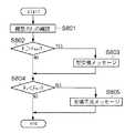
S800で、CPU100は、図8に示すフローチャートにより離型力の大きさに応じた処理を行う。S801で、CPU100は、ロードセル21により計測された離型力(複数のロードセル出力の平均値または最大値)を確認する。このときの基板1が図6のショット配置であり、基板1の周辺のショット1、ショット5、ショット21、ショット25は、ショットの一部が基板の外周からはみ出すエッジショットであるとする。エッジショットでは、ショットの一部の領域に対して樹脂が塗布され、当該樹脂が塗布されたショットの一部の領域に対してインプリント動作が行われる。CPU100は、インプリント動作を行うショットがエッジショットである場合、ロードセル21により検出された力と、樹脂が塗布された一部の領域の面積のショットの面積に対する割合とを用いて離型力FLを算出する。インプリント動作を行うショットが、ショットにおける全部の領域に対してインプリント動作が行われるショットであるならば、CPU100は、ロードセル21により検出された力を離型力FLと決定する。 In S800, the
図7に、図6のショット配置で番号順に各ショットのインプリントを行った場合の離型力の変化の例を示す。図7において、横軸はインプリント動作の回数を示し、図6のショット番号に相当する。縦軸は、図7aではロードセル21によって検出された型10に加えられた力を示し、図7bでは離型力FLを示し、単位はkgfである。図7aにおいて、4つのエッジショット(ショット1,5,21,25)では、他のフルサイズのショットに比べてインプリントされたパターンの面積が小さい。そのため、4つのエッジショットでは型10に加えられた力もパターンの面積に比例して小さい。離型力を同一基準にして比較を行うため、前述のショット面積比の換算を行って決定した各ショットの離型力FLの推移を図7bに示す。 FIG. 7 shows an example of a change in mold release force when imprinting each shot in the numerical order in the shot arrangement of FIG. In FIG. 7, the horizontal axis indicates the number of imprint operations, and corresponds to the shot number in FIG. The vertical axis shows the force applied to the
S802で、CPU100は、離型力FLが第1の閾値Fmaxより大きいかどうかの判定を行う。第1の閾値Fmaxは、(基準離型力F0+α)で示される力であり、αは基準離型力F0に対する離型力の許容増加分を示すものである。αの値は、形成されたパターンが離型時の樹脂の剥離によって崩壊が発生しない範囲の最大値とし、前述の基準離型力F0の決定と同じく、事前のテストインプリントなどにより決定し、メモリ110に保存しておく。このテストインプリントでは、実際にインプリントを重ねて、離型力の変化とともに、形成されたパターンの状態もチェックする。そして、基板上に形成されたパターンの凸部が欠けた状態や、形成されたパターン自体が基板から剥離した状態が観察されるようになった場合に、この時に計測された離型力から基準離型力F0を差し引いたものをαとする。また、αの値は、型を洗浄して離型剤の再塗布のたびにテストインプリントを行って更新する必要はない。実際にS802で使用するαの値は、計測誤差やインプリント条件の再現性を考慮して、上記で決めたαより10%ほど小さい値とするのが好ましい。なお、αの値は、図4の説明では省略したが、S101で、基準離型力F0と一緒にメモリ110からCPU100に読み込まれる。S802で、離型力FLが第1の閾値Fmax(=F0+α)より大きい場合、CPU100は、型の離型性が劣化し、型の交換が必要と判定し、S803に進む。S803で、CPU100は、型の交換をうながすメッセージを表示部120に表示する。また、CPU100は、リニアアクチュエータ15,15'又は基板ステージの駆動機構に、型10を取り出すための空間を作り出させる。S802で、離型力FLが第1の閾値Fmaxより小さい場合、CPU100は、型の交換は必要なしと判定し、S804に進める。 In S802, the
S804で、CPU100は、離型力FLを第2の閾値である最低離型力Fminと比較し、離型力FLが最低離型力Fminより小さいか否かの判定を行う。本発明者による検討では、光硬化樹脂に型10を押し付ける際に、型10のパターン凹部に気泡が残ってしまう充填不良が発生した場合、樹脂硬化後の型10の離型に必要とされる離型力が大幅に低下することが分かった。そこで、S804では、基準離型力F0より小さい(例えば、F0の60%程度の)離型力を最低離型力Fminと定義し、離型力FLがこれより小さい場合、CPU100は、充填不良が発生したと判定し、S805に進む。S805で、CPU100は、充填不良が発生したとの判定結果を表示部120に表示して、図8の処理(図5のS800)を終了する。一方、S804で、離型力FLが最低離型力Fminより大きい場合、CPU100は、充填不良が発生しなかったと判定し、同じく図8の処理を終了する。 In S804, the
ここで、図9に、一つの基板で25のショットにインプリント動作を行った場合の離型力の推移例を示し、図8の処理をもう一度説明する。図9において、横軸はインプリント動作の回数を示し、図6のショット番号に相当する。縦軸は離型力を示し、単位はkgfである。破線Aは型交換の判定基準である第1の閾値Fmaxを示し、破線Bは充填不良の判定基準である最低離型力Fminを示す。図9の例では、図8の処理により、ショット6は充填不良と判定され、ショット15で型交換が必要と判定されることになる。なお、型交換が必要と判定された場合、ショット16以降のインプリント動作は同じ型を用いて行われないため、実際には図9のショット16以降の離型力は記録されない。以上のようにして、図8の離型力の大きさに応じた処理、即ち図5のS800は実行される。 Here, FIG. 9 shows a transition example of the release force when the imprint operation is performed on 25 shots with one substrate, and the process of FIG. 8 will be described again. In FIG. 9, the horizontal axis indicates the number of imprint operations and corresponds to the shot number in FIG. The vertical axis represents the release force, and the unit is kgf. A broken line A indicates a first threshold value Fmax that is a determination criterion for mold replacement, and a broken line B indicates a minimum release force Fmin that is a determination criterion for defective filling. In the example of FIG. 9, the
ここで、図5の説明に戻ると、S800に続くS710で、CPU100は、基板1上の全ショットに対するインプリントが終了したか否か、又は、S800の結果、型交換が必要か否かを判定する。インプリントがなされていないショットがあり、かつ型交換が必要ない場合、S710の判定をnoで抜け、S702へ戻る。インプリントがなされていないショットが無い場合又は型交換が必要な場合、S710の判定をyesで抜け、S711に進む。S711で、CPU100は、基板1の回収(図4のS8)に備えて、所定の位置にXYステージ4を駆動する。 Here, returning to the description of FIG. 5, in S710 following S800, the
ここで基準離型力F0について補足する。基準離型力F0の値は事前にインプリントを行わずに、1枚目の基板の任意のショットへのインプリントの結果、得られる離型力で代用してもよい。例えば、1枚目の基板の最初のフルサイズショットや基板の中心付近のショットに対するインプリントの離型力を基準離型力F0としてもよい。また、型の剥離性の劣化具合がインプリント動作の回数に比して緩やかな場合は、ショットごとにS800の離型力のチェックを行わなくてもよい。例えば、当該基板の中心付近のショットや最終ショットといった特定ショットについてのみ、S800を実行するようにしてもよい。 Here, the reference mold release force F0 will be supplemented. The value of the reference release force F0 may be substituted with the release force obtained as a result of imprinting an arbitrary shot of the first substrate without performing imprinting in advance. For example, an imprint release force for the first full-size shot of the first substrate or a shot near the center of the substrate may be used as the reference release force F0. Further, when the degree of degradation of the mold peelability is moderate as compared with the number of imprint operations, it is not necessary to check the release force in S800 for each shot. For example, S800 may be executed only for a specific shot such as a shot near the center of the substrate or a final shot.
[実施例2]
次に、図10を参照して、実施例2におけるインプリント装置のインプリント動作について説明する。図10は、実施例2における、複数枚の基板に同じ型を使用してインプリント動作を行う場合のフローチャートである。図4のフローチャートと同じ機能を有するものは同じ番号を付し、その説明を省略する。図10において、S101からS8の動作は、実施例1である図4と同じである。[Example 2]
Next, an imprint operation of the imprint apparatus according to the second embodiment will be described with reference to FIG. FIG. 10 is a flowchart when the imprint operation is performed using the same mold for a plurality of substrates in the second embodiment. Components having the same functions as those in the flowchart of FIG. 4 are denoted by the same reference numerals, and description thereof is omitted. In FIG. 10, the operations from S101 to S8 are the same as those in FIG.
S8に続くS102で、CPU100は、1枚の基板の全ショットに対するインプリント動作が終了した時点で、メモリ110に記憶された離型力の推移から離型力が第1の閾値Fmaxを超える最初のショットを推定する。そして、CPU100は、離型力が第1の閾値Fmaxを超える最初のショットまでのショット数を算出し、型の交換時期を決定する。型の交換時期が、ある基板に対してインプリント動作を行っている途中となる場合、CPU100は、その基板に対するインプリント動作の開始前に型の交換を行うと決定する。 In S102 following S8, when the imprint operation for all the shots on one substrate is completed, the
ここで、図11を用いて、この型の交換時期の予測方法を説明する。図11は25ショットずつ、第1の基板、第2の基板の2枚の基板に連続してインプリント動作を行う場合の離型力の推移を示したものである。横軸は、インプリント動作回数である。図11において、第1の基板の25ショットのインプリントが終了した時点で、上記S102が実行される。その際、CPU100は、25ショット分の離型力の推移を直線近似または曲線近似して、次の第2の基板の25ショット分の離型力の推移を予測する。図11には、直線近似により求めた離型力の推移を近似式とともに破線で示す。この場合、前述の第1の閾値Fmaxが12に設定されていたとする。そうすると、一点鎖線Cで示す33回目(第2の基板のショット8)のインプリントで、予想される離型力が第1の閾値Fmaxを超えることになる。即ち、基板1のインプリントが終了した時点のインプリント可能ショット数は、1つ少ない7となる。これは、次の第2の基板で予定されているショット数25より小さいため、S102では第2の基板のインプリント動作を開始する前に型の交換が必要と判定される。この判定の結果、図示しての説明は省略するが、図8で説明したS803と同様、型の交換をうながすメッセージが表示部120に表示される。S102に続く、S9とS10は図4と同じである。 Here, a prediction method of this type of replacement time will be described with reference to FIG. FIG. 11 shows the transition of the mold release force when the imprint operation is continuously performed on the two substrates, the first substrate and the second substrate, every 25 shots. The horizontal axis represents the number of imprint operations. In FIG. 11, when the 25-shot imprint of the first substrate is completed, the above S102 is executed. At that time, the
最後に、S103で、メモリ110に対して、使用した型のショット毎の離型力の追記と、最後に転写された基板についてS102で算出され予測されたインプリント可能ショット数の更新とを行う。以上で、図10の複数の基板へのインプリント動作を終了する。 Finally, in S103, the release force for each shot of the used mold is added to the
以上、図4及び図10を用いて、複数の基板に対してインプリントを行う場合におけるインプリント装置の動作について説明した。なお、図4及び図10で型交換が必要と判定された場合、型10をインプリント装置から回収し、洗浄する一方、交換後の型を用いてインプリント動作を自動的に継続するようにしてもよい。これにより、同一基板、別基板に対してインプリント動作を継続して行うことができる。なお、実施例では、型の転写履歴の保存と参照はメモリ110を使用して行うように説明したが、メモリ110はインプリント装置上に設置しなくてもよい。例えば、メモリ110の替わりに、ネットワークを介して接続されるデータベースを別途用意して、複数のインプリント装置で型の転写履歴を共有するようにしてもよい。 The operation of the imprint apparatus when imprinting on a plurality of substrates has been described above with reference to FIGS. 4 and 10. 4 and 10, when it is determined that the mold needs to be replaced, the
以上説明したように、本発明によれば、基板上の複数のショットにステップ・アンド・リピート方式でインプリント動作を行う際に、1枚の基板についてのインプリントの途中で型交換の要否を判定することができる。その結果、型の剥離性の劣化によるパターン剥離などの不良ショットの発生を防止することが可能となり、歩留りの高いインプリント装置を提供することができる。また、離型力を比較して充填不良の判定を行うことで、インプリント後の検査で不良ショットの確認を容易にすることもできる。 As described above, according to the present invention, when imprinting is performed on a plurality of shots on a substrate by the step-and-repeat method, it is necessary to exchange molds during imprinting for one substrate. Can be determined. As a result, it is possible to prevent the occurrence of defective shots such as pattern peeling due to deterioration of the mold peeling property, and to provide an imprint apparatus with a high yield. Further, by comparing the release force and determining the filling failure, it is possible to easily check the defective shot in the inspection after imprinting.
[物品の製造方法]
物品としてのデバイス(半導体集積回路素子、液晶表示素子等)の製造方法は、上述したインプリント装置を用いて基板(ウエハ、ガラスプレート、フィルム状基板)にパターンを転写(形成)する工程を含む。さらに、該製造方法は、パターンを転写された基板をエッチングする工程を含みうる。なお、パターンドメディア(記録媒体)や光学素子などの他の物品を製造する場合には、該製造方法は、エッチングの代わりに、パターンを転写された基板を加工する他の処理を含みうる。
以上、本発明の実施の形態を説明してきたが、本発明はこれらの実施の形態に限定されず、その要旨の範囲内において様々な変形及び変更が可能である。[Product Manufacturing Method]
A method for manufacturing a device (semiconductor integrated circuit element, liquid crystal display element, etc.) as an article includes a step of transferring (forming) a pattern onto a substrate (wafer, glass plate, film-like substrate) using the above-described imprint apparatus. . Further, the manufacturing method may include a step of etching the substrate to which the pattern is transferred. In the case of manufacturing other articles such as patterned media (recording media) and optical elements, the manufacturing method may include other processing for processing the substrate to which the pattern is transferred instead of etching.
As mentioned above, although embodiment of this invention was described, this invention is not limited to these embodiment, A various deformation | transformation and change are possible within the range of the summary.
Claims (8)
Translated fromJapanese型を支持する支持体と、
基板を支持する基板ステージと、
前記型に加えられた力を検出する検出器と、
前記支持体と前記基板ステージとの間に、前記支持体に支持された前記型を取り外すための空間を作り出す機構と、
制御部と、
を備え、
前記制御部は、硬化した樹脂から前記型を引き離すために要する離型力を前記検出器の検出結果に基づいて決定し、前記決定された離型力を第1の閾値と比較し、前記決定された離型力が前記第1の閾値より大きいならば前記機構に前記空間を作り出させる、ことを特徴とするインプリント装置。An imprint apparatus that applies an imprint operation for each shot of the substrate by applying a resin to the substrate and curing the resin in a state in which a mold is pressed against the applied resin.
A support that supports the mold;
A substrate stage for supporting the substrate;
A detector for detecting the force applied to the mold;
A mechanism for creating a space for removing the mold supported by the support body between the support body and the substrate stage;
A control unit;
With
The control unit determines a release force required to separate the mold from the cured resin based on a detection result of the detector, compares the determined release force with a first threshold, and determines the determination. An imprint apparatus, wherein if the released mold release force is greater than the first threshold, the mechanism creates the space.
前記制御部は、前記決定された離型力が前記第1の閾値より大きいならば前記型の交換をうながすメッセージを前記表示部に表示させる、ことを特徴とする請求項1又は請求項2に記載のインプリント装置。A display unit;
3. The control unit according to claim 1, wherein the control unit displays a message prompting replacement of the mold on the display unit if the determined release force is larger than the first threshold value. The imprint apparatus described.
ショットにおける全部の領域に対して前記インプリント動作が行われたならば、前記検出器により検出された力を前記離型力と決定し、
ショットの一部が前記基板の外周からはみ出し、樹脂が塗布された、ショットの一部の領域に対して前記インプリント動作が行われたならば、前記検出器により検出された力と、前記樹脂が塗布された一部の領域の面積の前記ショットの面積に対する割合とを用いて前記離型力を算出する、ことを特徴とする請求項1乃至請求項3のいずれか1項に記載のインプリント装置。The controller is
If the imprint operation is performed on the entire area in the shot, the force detected by the detector is determined as the release force,
If the imprint operation is performed on a partial area of the shot where a part of the shot protrudes from the outer periphery of the substrate and resin is applied, the force detected by the detector and the resin 4. The mold release force according to claim 1, wherein the mold release force is calculated using a ratio of an area of a part of the region to which the coating is applied to an area of the shot. 5. Printing device.
前記制御部は、前記記憶部に記憶された離型力の推移から離型力が前記第1の閾値を超える最初のショットを推定することにより前記型の交換時期を決定することを特徴とする請求項1乃至請求項4のいずれか1項に記載のインプリント装置。A storage unit for storing the determined release force;
The control unit determines a replacement time of the mold by estimating a first shot in which a release force exceeds the first threshold from a transition of the release force stored in the storage unit. The imprint apparatus according to any one of claims 1 to 4.
前記工程で前記パタ−ンを形成された基板を加工する工程と、
を含む、ことを特徴とする物品の製造方法。Forming a pattern on a substrate using the imprint apparatus according to any one of claims 1 to 7;
Processing the substrate on which the pattern is formed in the step;
A method for producing an article comprising:
Priority Applications (2)
| Application Number | Priority Date | Filing Date | Title |
|---|---|---|---|
| JP2010004445AJP2011146447A (en) | 2010-01-12 | 2010-01-12 | Imprint apparatus and article manufacturing method |
| US13/004,469US8770964B2 (en) | 2010-01-12 | 2011-01-11 | Imprint apparatus and article manufacturing method |
Applications Claiming Priority (1)
| Application Number | Priority Date | Filing Date | Title |
|---|---|---|---|
| JP2010004445AJP2011146447A (en) | 2010-01-12 | 2010-01-12 | Imprint apparatus and article manufacturing method |
Publications (1)
| Publication Number | Publication Date |
|---|---|
| JP2011146447Atrue JP2011146447A (en) | 2011-07-28 |
Family
ID=44257919
Family Applications (1)
| Application Number | Title | Priority Date | Filing Date |
|---|---|---|---|
| JP2010004445AWithdrawnJP2011146447A (en) | 2010-01-12 | 2010-01-12 | Imprint apparatus and article manufacturing method |
Country Status (2)
| Country | Link |
|---|---|
| US (1) | US8770964B2 (en) |
| JP (1) | JP2011146447A (en) |
Cited By (5)
| Publication number | Priority date | Publication date | Assignee | Title |
|---|---|---|---|---|
| JP2012135987A (en)* | 2010-12-27 | 2012-07-19 | Hoya Corp | Imprinting apparatus and transfer defect detection method |
| JP2015056598A (en)* | 2013-09-13 | 2015-03-23 | 公立大学法人大阪府立大学 | Pattern formation device and pattern formation method using the same |
| JP2015179806A (en)* | 2013-09-18 | 2015-10-08 | キヤノン株式会社 | Method for manufacturing film, method for manufacturing optical component, method for manufacturing circuit board, method for manufacturing electronic component, and photocurable composition |
| WO2017099492A1 (en)* | 2015-12-08 | 2017-06-15 | 주식회사 기가레인 | Imprint device and method |
| JP2023141408A (en)* | 2022-03-24 | 2023-10-05 | キヤノン株式会社 | Imprint device, imprint method, computer program, and method for manufacturing article |
Families Citing this family (2)
| Publication number | Priority date | Publication date | Assignee | Title |
|---|---|---|---|---|
| JP5769451B2 (en)* | 2011-03-07 | 2015-08-26 | キヤノン株式会社 | Imprint apparatus and article manufacturing method |
| JP6768409B2 (en)* | 2016-08-24 | 2020-10-14 | キヤノン株式会社 | Imprint device and article manufacturing method |
Family Cites Families (5)
| Publication number | Priority date | Publication date | Assignee | Title |
|---|---|---|---|---|
| MY164487A (en) | 2002-07-11 | 2017-12-29 | Molecular Imprints Inc | Step and repeat imprint lithography processes |
| JP4574240B2 (en)* | 2004-06-11 | 2010-11-04 | キヤノン株式会社 | Processing apparatus, processing method, device manufacturing method |
| JP4533358B2 (en)* | 2005-10-18 | 2010-09-01 | キヤノン株式会社 | Imprint method, imprint apparatus and chip manufacturing method |
| JP2008246729A (en) | 2007-03-29 | 2008-10-16 | Sumitomo Heavy Ind Ltd | Molding machine and molding method using the same |
| JPWO2008129962A1 (en)* | 2007-04-19 | 2010-07-22 | コニカミノルタホールディングス株式会社 | Molding apparatus and control method thereof |
- 2010
- 2010-01-12JPJP2010004445Apatent/JP2011146447A/ennot_activeWithdrawn
- 2011
- 2011-01-11USUS13/004,469patent/US8770964B2/enactiveActive
Cited By (10)
| Publication number | Priority date | Publication date | Assignee | Title |
|---|---|---|---|---|
| JP2012135987A (en)* | 2010-12-27 | 2012-07-19 | Hoya Corp | Imprinting apparatus and transfer defect detection method |
| JP2015056598A (en)* | 2013-09-13 | 2015-03-23 | 公立大学法人大阪府立大学 | Pattern formation device and pattern formation method using the same |
| JP2015179806A (en)* | 2013-09-18 | 2015-10-08 | キヤノン株式会社 | Method for manufacturing film, method for manufacturing optical component, method for manufacturing circuit board, method for manufacturing electronic component, and photocurable composition |
| KR20170094561A (en)* | 2013-09-18 | 2017-08-18 | 캐논 가부시끼가이샤 | Method of producing film, method of producing optical component, method of producing circuit board, method of producing electronic component, and photocurable composition |
| US10338467B2 (en) | 2013-09-18 | 2019-07-02 | Canon Kabushiki Kaisha | Method of producing film |
| KR102100239B1 (en) | 2013-09-18 | 2020-04-13 | 캐논 가부시끼가이샤 | Method of producing film, method of producing optical component, method of producing circuit board, method of producing electronic component, and photocurable composition |
| WO2017099492A1 (en)* | 2015-12-08 | 2017-06-15 | 주식회사 기가레인 | Imprint device and method |
| CN108292592A (en)* | 2015-12-08 | 2018-07-17 | 吉佳蓝科技股份有限公司 | Imprinting apparatus and method |
| CN108292592B (en)* | 2015-12-08 | 2022-04-01 | 吉佳蓝科技股份有限公司 | Imprint apparatus and method |
| JP2023141408A (en)* | 2022-03-24 | 2023-10-05 | キヤノン株式会社 | Imprint device, imprint method, computer program, and method for manufacturing article |
Also Published As
| Publication number | Publication date |
|---|---|
| US20110169181A1 (en) | 2011-07-14 |
| US8770964B2 (en) | 2014-07-08 |
Similar Documents
| Publication | Publication Date | Title |
|---|---|---|
| JP5173944B2 (en) | Imprint apparatus and article manufacturing method | |
| US20220026800A1 (en) | Imprint apparatus, imprinting method, and method of manufacturing product | |
| US9280047B2 (en) | Imprint apparatus and article manufacturing method | |
| JP2010080630A (en) | Stamping device and method of manufacturing article | |
| JP2011146447A (en) | Imprint apparatus and article manufacturing method | |
| US9254608B2 (en) | Imprint apparatus, imprint method, and method of manufacturing article | |
| KR101889632B1 (en) | Imprint apparatus, imprint method, and article manufacturing method | |
| US8404169B2 (en) | Imprint apparatus and method of manufacturing article | |
| JP5371349B2 (en) | Imprint apparatus and article manufacturing method | |
| JP2010080714A (en) | Stamping device, and method of manufacturing article | |
| US10331027B2 (en) | Imprint apparatus, imprint system, and method of manufacturing article | |
| JP2012178470A (en) | Imprint device and device manufacturing method | |
| JP2016096269A (en) | Imprint device and manufacturing method of article | |
| JP2022018203A (en) | Information processing apparatus, determination method, inspection device, molding device, and method for manufacturing article | |
| US20160320697A1 (en) | Imprint apparatus, imprint method, and article manufacturing method | |
| JP7324051B2 (en) | Lithographic apparatus, method of manufacturing and control of article | |
| US20240025106A1 (en) | Control method, molding apparatus, and article manufacturing method | |
| US11759994B2 (en) | Imprint apparatus, imprint method, and article manufacturing method | |
| US20210379800A1 (en) | Imprint device, article manufacturing method, and measuring method for imprint device | |
| JP2021077771A (en) | Imprint device, imprint method and manufacturing method for article |
Legal Events
| Date | Code | Title | Description |
|---|---|---|---|
| A300 | Application deemed to be withdrawn because no request for examination was validly filed | Free format text:JAPANESE INTERMEDIATE CODE: A300 Effective date:20130402 |