JP2011146143A - Microwave processing device - Google Patents
Microwave processing deviceDownload PDFInfo
- Publication number
- JP2011146143A JP2011146143AJP2010003770AJP2010003770AJP2011146143AJP 2011146143 AJP2011146143 AJP 2011146143AJP 2010003770 AJP2010003770 AJP 2010003770AJP 2010003770 AJP2010003770 AJP 2010003770AJP 2011146143 AJP2011146143 AJP 2011146143A
- Authority
- JP
- Japan
- Prior art keywords
- door
- voltage
- unit
- power supply
- processing apparatus
- Prior art date
- Legal status (The legal status is an assumption and is not a legal conclusion. Google has not performed a legal analysis and makes no representation as to the accuracy of the status listed.)
- Pending
Links
Images


Landscapes
- Control Of High-Frequency Heating Circuits (AREA)
Abstract
Translated fromJapaneseDescription
Translated fromJapanese本発明は、半導体素子を用いて構成したマイクロ波発生部を備えたマイクロ波処理装置に関するものである。 The present invention relates to a microwave processing apparatus including a microwave generation unit configured using a semiconductor element.
従来のマイクロ波処理装置は、一般には電子レンジに代表されるようにマイクロ波発生手段にマグネトロンと称される真空管を用いているものが一般的である。 A conventional microwave processing apparatus generally uses a vacuum tube called a magnetron as a microwave generating means as represented by a microwave oven.
近年、このマグネトロンに代えて、窒化ガリウム(GaN)などの半導体素子を用いた高周波加熱装置の開発が進められている。マイクロ波は電子レンジに係わらず誘電加熱を応用する機器に展開可能である(例えば、特許文献1参照)。 In recent years, a high-frequency heating apparatus using a semiconductor element such as gallium nitride (GaN) instead of the magnetron has been developed. Microwaves can be developed in devices that apply dielectric heating regardless of the microwave oven (see, for example, Patent Document 1).
GaNを用いたときの効果としては、小型、軽量かつ容易に周波数や位相を可変することができることである。 The effect of using GaN is that the frequency and phase can be easily varied in a small size and light weight.
一方、従来マグネトロンや、それを付勢する電源に関しては容積が大きく、重量が重いため、マイクロ波を主熱源あるいは補助熱源として利用するアイデアは多く存在するが実用には至っていなかった。特許文献1ではマイクロ波漏洩に対する安全性としての扉体開閉に連動して漏洩電波を停止する安全装置に関する技術が開示されている。 On the other hand, the conventional magnetron and the power source for energizing the magnetron have a large volume and a heavy weight, so there are many ideas to use the microwave as a main heat source or an auxiliary heat source, but they have not been put into practical use.
しかし、従来技術の構成では、扉体と連動してマイクロ波発生手段への商用電源の供給を停止する安全スイッチを二重に設けることにより、扉体の開放にともなう漏洩電波を阻止し安全性の担保を図ろうとするものであったが、GaNを用いた固体発振装置の場合ノーマリーON型FET(外部から制御信号が入っていない状態でトラジスタ動作する)を用いることが一般的で電源供給を一斉遮断してしまうと、トランジスタが破壊してしまうという課題があった。 However, in the configuration of the prior art, a safety switch that stops the supply of commercial power to the microwave generating means in conjunction with the door body is doubled to prevent leakage radio waves due to the door body opening and safety However, in the case of a solid-state oscillation device using GaN, it is common to use a normally-on type FET (transistor operation without a control signal from the outside) and supply power. There was a problem that the transistors would be destroyed if they were shut off all at once.
例えば、ノーマリーONのGaNトラジスタであれば、ドレイン−ソース間に電圧が印加された状態でゲートバイアス電圧を除去してしまうと、トランジスタ内部でショート回路が形成され短絡破壊してしまう。 For example, in the case of a normally-on GaN transistor, if the gate bias voltage is removed while a voltage is applied between the drain and source, a short circuit is formed inside the transistor, causing a short circuit breakdown.
本発明は、上記従来の課題を解決するもので、扉体と連動した機械的接点を有し、ノーマリーONのトランジスタを有するマイクロ波処理装置においても、トランジスタを破壊しない信頼性が高く安全性に優れたマイクロ波処理装置を提供することを目的とする。 The present invention solves the above-mentioned conventional problems, and in a microwave processing apparatus having a mechanical contact interlocked with a door body and having a normally ON transistor, the transistor is not damaged and is highly reliable and safe. An object is to provide an excellent microwave processing apparatus.
上記従来の課題を解決するために、本発明に係わるマイクロ波処理装置は、加熱室と、加熱室に被加熱物を収納自在とし閉時にはマイクロ波の漏洩を阻止するドアと、商用電源をAC−DC変換し正極電圧供給部と負極電圧供給部とバイアス電圧供給部に所望の電圧を供給する電源部と、パワーユニットへの電源部からの電力供給はドアの閉時と連動して閉成する第一のドアスイッチを介して所望の電圧を正極電圧供給部から供給するもので、
翻ってドア開時(ドアが開かれた時)は第一のドアスイッチの開成によって瞬時に正極電圧供給部からの正極電圧印加を除去するものである。また、バイアス電圧供給部からのバイアス電圧供給はドアの開閉と非連動で常に供給されている。In order to solve the above-described conventional problems, a microwave processing apparatus according to the present invention includes a heating chamber, a door that can store an object to be heated in the heating chamber, and prevents leakage of microwaves when closed, and a commercial power source is connected to an AC power supply. -DC conversion to supply a desired voltage to the positive voltage supply unit, the negative voltage supply unit, and the bias voltage supply unit, and the power supply from the power supply unit to the power unit is closed in conjunction with the closing of the door. A desired voltage is supplied from the positive voltage supply unit via the first door switch.
In turn, when the door is opened (when the door is opened), the positive voltage application from the positive voltage supply is instantaneously removed by opening the first door switch. Also, the bias voltage supply from the bias voltage supply unit is always supplied without being interlocked with the opening and closing of the door.
上記構成により、パワーユニットのノーマリーON型のトランジスタはドア開と連動して第一のドアスイッチが開成し電圧が除去されかつバイアス電圧印加は維持されるためトランジスタの破壊を生じることなくマイクロ波処理装置のマイクロ波発振を停止することができる。 With the above configuration, the normally ON type transistor of the power unit opens the first door switch in conjunction with the opening of the door, the voltage is removed, and the bias voltage application is maintained, so that the microwave processing device does not break down without causing transistor breakdown Can stop the microwave oscillation.
本発明のマイクロ波処理装置は、ノーマリーON型のトランジスタを用いたパワーユニットにおいても、ドアと連動した機械的接点を持つドアスイッチで電力供給を瞬時に停止し、ドアが開放されてもトランジスタが破壊することなくマイクロ波漏洩が発生しない、安全でかつ信頼性の高いマイクロ波処理装置を提供するものである。 In the microwave processing apparatus of the present invention, even in a power unit using a normally-on type transistor, the power supply is instantaneously stopped by a door switch having a mechanical contact linked to the door, and the transistor is destroyed even if the door is opened. Therefore, the present invention provides a safe and highly reliable microwave processing apparatus that does not cause microwave leakage.
第1の発明は、被加熱物を収容する加熱室と、前記加熱室から機外へ電波の漏洩を遮断する開閉自在のドアと、マイクロ波の基準信号を作成する発振部と、前記発振部の出力を受け半導体素子を用いた複数段のアンプでかつ少なくとも複数段のアンプの最終段はノーマリーON型のFETを用いた半導体で構成された電力増幅を行うパワーユニットと、パワーユニットから出力されるマイクロ波電力を放射するアンテナと、パワーユニットのドレイン又はコレクタに印加される正極電圧と、エミッタ又はソースに印加される負極電圧と、ベース又はゲートに印加されるバイアス電圧を作成する電源部とからなり、第一のドアスイッチの閉成によりパワーユニットの前記正極電圧供給部からドレイン又はコレクタに正極電圧を供給する構成とするものである。 According to a first aspect of the present invention, there is provided a heating chamber that houses an object to be heated, an openable / closable door that blocks leakage of radio waves from the heating chamber to the outside of the apparatus, an oscillating unit that creates a microwave reference signal, and the oscillating unit The power unit is a multi-stage amplifier using semiconductor elements and at least the final stage of the multi-stage amplifier is composed of a semiconductor using a normally-on type FET, and a power unit for amplifying power and a micro output from the power unit An antenna that radiates wave power, a positive voltage applied to the drain or collector of the power unit, a negative voltage applied to the emitter or source, and a power supply that creates a bias voltage applied to the base or gate, A positive voltage is supplied to the drain or collector from the positive voltage supply part of the power unit by closing the first door switch. It is intended.
これにより、ノーマリーON型のFETはゲート電圧がかかっていない時にドレイン電圧が印加され短絡電流が流れ破壊するという破壊モードを回避することができる。このことにより、電源部からパワーユニットへのバイアス電圧が供給された状態で正極電圧供給部からドレイン又はコレクタに正極電圧がパワーユニットに供給されるため安全にマイクロ波発生が可能な状態とすることができる。 Thereby, the normally ON type FET can avoid the destruction mode in which the drain voltage is applied and the short-circuit current flows and breaks when the gate voltage is not applied. Thus, since the positive voltage is supplied to the power unit from the positive voltage supply unit to the drain or collector while the bias voltage is supplied from the power supply unit to the power unit, it is possible to safely generate microwaves. .
また、ドアが開かれた時、第一のドアスイッチの開成により電源部の正極電圧供給部からドレイン又はコレクタに正極電圧の供給が瞬時に遮断されるが、バイアス電圧は供給され続けるためノーマリーON型のFETを有していても動作中のドア開によって半導体が破壊されることはなく高い安全性と信頼性を有するマイクロ波処理装置を提供することができる。 In addition, when the door is opened, the supply of the positive voltage from the positive voltage supply unit of the power supply unit to the drain or collector is instantaneously cut off by the opening of the first door switch. Even if it has a type FET, the semiconductor is not destroyed by opening the door during operation, and a microwave processing apparatus having high safety and reliability can be provided.
第2の発明は、ドアが閉じられるとき閉成する第二のドアスイッチを設け電源部への電
力供給を行う構成としたものである。In the second aspect of the present invention, a second door switch that closes when the door is closed is provided to supply power to the power supply unit.
これにより、第一のドアスイッチが溶着しても第二のドアスイッチが正常に作動する二重の安全機構構成を有することになり安全で信頼性の高いマイクロ波処理装置を提供することができる。 Thereby, even if the first door switch is welded, it has a double safety mechanism configuration in which the second door switch operates normally, and a safe and highly reliable microwave processing apparatus can be provided. .
第3の発明は、第一のドアスイッチの接点と直列に接続されるノーマリーオープンの接点をもつリレーと、商用電源の印加の有無を検出可能なメイン制御部とを備えたものである。 The third invention includes a relay having a normally open contact connected in series with the contact of the first door switch, and a main control unit capable of detecting the presence or absence of application of commercial power.
これにより、リレーはメイン制御部からの指令信号によって電源部への商用電源断後に開成する構成とし、商用電源印加直後からはバイアス電圧供給部の電圧が確立するまで十分遅延時間を有した後にリレーに閉成信号を出力し半導体のバイアス電圧がスレッショルドを超えアクティブ状態になった後に正極電圧が印加される構成とすることからノーマリーON型のFETはゲート電圧がかかっていない時にドレイン電圧が印加され短絡電流が流れ破壊するという破壊モードを回避することができる。その結果、機器の破壊が発生しない信頼性の高いマイクロ波処理装置を提供することができる。 As a result, the relay is configured to open after the commercial power supply to the power supply unit is cut off by a command signal from the main control unit, and immediately after the commercial power supply is applied, the relay has a sufficient delay time until the voltage of the bias voltage supply unit is established. Since normally closed FET is output and positive voltage is applied after the semiconductor bias voltage exceeds the threshold and becomes active, drain voltage is applied to normally ON type FET when no gate voltage is applied. A destruction mode in which a short-circuit current flows and breaks can be avoided. As a result, it is possible to provide a highly reliable microwave processing apparatus that does not cause destruction of equipment.
第4の発明は、バイアス電圧供給部と負極電圧供給部との間に商用電源断時の電圧下降時定数が緩やかになるような容量性インピーダンスを備えものである。 According to a fourth aspect of the present invention, a capacitive impedance is provided between the bias voltage supply unit and the negative voltage supply unit so that the voltage drop time constant when the commercial power supply is cut off becomes gradual.
これにより、商用電源断時にノーマリーON型のFETのゲートのバイアス電圧が長時間ゲートのスレッショルド電圧を超える状態が維持されるため、ドレイン電圧が印加された状態でバイアス電圧が低下してしまいノーマリーON型のFETの破壊モードを回避することができ信頼性の高いマイクロ波処理装置を提供することができる。 As a result, the state in which the bias voltage of the gate of the normally-on type FET exceeds the gate threshold voltage for a long time when the commercial power supply is cut off is maintained, so that the bias voltage is lowered when the drain voltage is applied and the normally-on FET is normally on. Therefore, it is possible to provide a highly reliable microwave processing apparatus that can avoid the destruction mode of the type FET.
第5の発明は、正極電圧供給部と負極電圧供給部との間に放電抵抗を備えるものである。商用電源断時後、ノーマリーON型のFETのゲート電圧がスレッショルドを下回る前に正極電圧を成立させる充電電荷が速やかに零電圧となるため、ノーマリーON型のFETの破壊モードを回避する信頼性の高いマイクロ波処理装置を提供するものである。 5th invention provides a discharge resistance between a positive electrode voltage supply part and a negative electrode voltage supply part. Since the charge charge that establishes the positive voltage quickly becomes zero voltage before the gate voltage of the normally-on type FET falls below the threshold after the commercial power supply is cut off, it is reliable to avoid the destruction mode of the normally-on type FET A high microwave processing apparatus is provided.
第6の発明は、商用電源の後に配した電流ヒューズと、第二のドアスイッチの後に配したドア開時に閉成するドアと連動した第三のドアスイッチとからなる。 6th invention consists of the 3rd door switch interlock | cooperated with the current fuse distribute | arranged after the commercial power supply, and the door closed when the door distribute | arranged after the 2nd door switch opened.
これにより、万一第二のドアスイッチが溶着したとき第三のドアスイッチを通じた閉回路が形成され瞬時に電流ヒューズを溶断し機器の動作を停止させるためドアのオープンによってユーザーがマイクロ波を暴露するという危険な状況を一切生じさせない安全性の高いマイクロ波処理装置を提供することができる。 As a result, when the second door switch is welded, a closed circuit is formed through the third door switch, and the user is exposed to microwaves by opening the door to instantaneously blow the current fuse and stop the operation of the device. It is possible to provide a highly safe microwave processing apparatus that does not cause any dangerous situation.
以下、本発明の実施の形態について、図面を参照しながら説明する。なお、この実施の形態によって本発明が限定されるものではない。 Hereinafter, embodiments of the present invention will be described with reference to the drawings. Note that the present invention is not limited to the embodiments.
(実施の形態1)
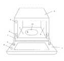
図1は、本発明の第1の実施の形態におけるマイクロ波処理装置の概観斜視図である。ドア1は被加熱物10を収納する。ヒンジ7はドア1を支え、ヒンジ取付け穴A8を通して筐体内部に出入り可能となっており終端は筐体に固定された螺旋バネ(図示していない)に取り付けられており、取付け穴B9を通してドア1に係合されている。(Embodiment 1)
FIG. 1 is a schematic perspective view of a microwave processing apparatus according to a first embodiment of the present invention. The
このような構成によって、ドア1が閉まりかけるとバネの弾性により強制的にドア1は閉じる。 With such a configuration, when the
載置板3は被加熱物10を載置するためのもので、マイクロ波を透過させ自己の誘電損失も少ない材料が選定されている。金属性のオーブン5は被加熱物10を収納するためのもので、ボディー2は筐体全体を覆う。 The
ドア1が閉められると、ドア1の表面に突起状に形成したプッシュ突起物4がスイッチ穴6を通して機械室内部のマイクロスイッチを押し、ドア1が閉められたことを検知する構成となっている。 When the
なお、以下の記述は、マイクロ波処理装置の事例として電子レンジを用いたものであるが、電子レンジに限定するものでないことは言うまでもない。 In addition, although the following description uses a microwave oven as an example of a microwave processing apparatus, it cannot be overemphasized that it is not limited to a microwave oven.
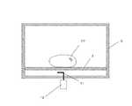
図2は、マイクロ波処理装置の要部断面図である。マイクロ波はオーブン5内にアンテナ11を介して照射され、内部の載置板3の上に載せられた被加熱物10を誘電加熱する。当然、外部にマイクロ波が漏洩しないようにドア1で密閉する。マイクロ波発生源の中核をなすものはパワーユニット12であり、ここで2.45GHzの大電力のマイクロ波が創出され、アンテナ11介してオーブン5の内部に放射される。 FIG. 2 is a cross-sectional view of a main part of the microwave processing apparatus. Microwaves are irradiated into the oven 5 via the
マイクロ波発生手段は、一般的に2極自励発振管であるマグネトロンが最もポピュラーなデバイスであるが、本発明では半導体による固体発振を使用している。 As the microwave generating means, a magnetron which is a bipolar self-excited oscillation tube is generally the most popular device, but in the present invention, solid-state oscillation by a semiconductor is used.
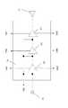
図3は、パワーユニット12の内部構成を示すブロック構成図である。アンプ段は、初段パワーアンプ25と中段パワーアンプ26と最終段パワーアンプ27とで構成されている。アンプの増幅には高周波で大電力を扱え、かつ高効率の化合物半導体であるGaN(窒化ガリウム)を用いたノーマリーON(操作信号をいれないとき導通する型のトランジスタ)のFETが用いられている。 FIG. 3 is a block configuration diagram showing the internal configuration of the
Vgbは、ゲートバイアスで約−5Vのバイアス電圧を印加してOFFになる。一方、信号は無い場合ONとなる。Vddはドレイン電圧、ソースは負電圧(GND)になっている。 Vgb is turned off when a bias voltage of about −5 V is applied as a gate bias. On the other hand, it is ON when there is no signal. Vdd is a drain voltage, and the source is a negative voltage (GND).
このアンプ段は、微弱な電力の信号を作る発振器部21から0dBm信号をパワーユニット12に創出し、約53dBmの電力を得ている。そのマイクロ波はアンテナ11でオーブン庫内に照射される。 The amplifier stage creates a 0 dBm signal in the
ここで、GaNのFETの特徴としてはVddに電圧が印加された状態で、Vgbがスレッショルド以下にして非アクティブにすると半導体内部で短絡状態が生じ破壊に至ってしまうという特性をもっている。 Here, as a feature of the GaN FET, when a voltage is applied to Vdd and Vgb is made below the threshold value to make it inactive, a short circuit state occurs inside the semiconductor, leading to destruction.
図4を用いて本発明の制御回路全体の動作を説明する。電流ヒューズ13は、商用電源16に直接接続される。マイクロスイッチである第二のドアスイッチ14はドア1と連動して接点が開閉する。第三のドアスイッチ15はドア1と連動して接点が開閉する。 The overall operation of the control circuit of the present invention will be described with reference to FIG. The
ここで、第二のドアスイッチ14が万一溶着したとき、商用電源16→電流ヒューズ13→第二のドアスイッチ14→第三のドアスイッチ15→商用電源16のショートサーキットで電流ヒューズ13を短絡電流によって溶断させ後段への電力供給を停止させる安全回路を構成している。 Here, when the
ドア1との連動性について述べておくと、第二のドアスイッチ14はドア1がオープンの場合開成し、ドア1がクローズの場合閉成する。第三のドアスイッチ15は2接点をも
ちドア1がオープンの場合後段に電力を送るべく閉成し、ドア1がクローズの場合前述したショートサーキットを形成する方向に閉成する。When the interlocking with the
これによって、ドア1と連動して接点が開閉するスイッチと、それを監視し溶着した場合ショートサーキットを形成して電流ヒューズ13を溶断して入力を遮断するスイッチの二重の安全回路を形成している。 As a result, a double safety circuit comprising a switch whose contact is opened and closed in conjunction with the
電源部17は、絶縁トランスを有するDC−DCコンバータ30と正極電圧供給部18とバイアス電圧供給部20とGNDたる負極電圧供給部19、正極電圧供給部18と負極電圧供給部19の間に設けられた放電抵抗28、バイアス電圧供給部20と負極電圧供給部19の間に設けられた容量性インピーダンスである電解コンデンサ29からなる。 The
負極電圧供給部19の負極電圧とバイアス電圧供給部20のバイアス電圧Vgbとは、直接パワーユニット12に供給される。一方、正極電圧供給部18の正極電圧Vddは、ドア1と連動して接点が開閉する第一のドアスイッチ22とリレー23を通じてパワーユニット12に供給される。ここで、第一のドアスイッチ22は、ドア1がオープンの時接点が開成しドア2がクローズの時接点が閉成する構成となっている。 The negative voltage of the negative
リレー23は、機器全体をコントロールするメイン制御部24によって開閉が制御される。ドアがクローズの時、後述する意図的なタイミングでリレーコイルに閉成の信号を送信し第一のドアスイッチ22、リレー23を通じてパワーユニット12にVdd電圧を供給する。そうすることによってパワーユニット12は作動し発振部21の信号は電力増幅されアンテナ11からマイクロ波が照射される。 The
このような構成にすることによって、ドア1と連動して接点が開閉する2つのスイッチ(第一のドアスイッチ22と第二のドアスイッチ14の二重の発振停止装置を有することになる)で、二重にドア1のオープン時のマイクロ波漏洩によるユーザーへの人体暴露を厳重に回避する構成を実現している。 With such a configuration, two switches that open and close in conjunction with the door 1 (have a double oscillation stop device of the
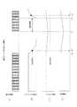
それでは、図5を用いて各部の電圧波形の商用電源が途中で欠落した時のタイミングチャートを示し、本発明の制御シーケンスを説明する。 Now, a timing chart when the commercial power supply of the voltage waveform of each part is lost on the way is shown using FIG. 5, and the control sequence of the present invention will be described.
この場合は、電解コンデンサ29と放電抵抗28がないケースである。図5(イ)は商用電源のエンベロープ波形、図5(ロ)はリレーのコイル電圧、図5(ハ)はバイアス電圧、図5(ニ)は正極電圧である。 In this case, the
このケースでは、(a)点で電源コンセントが抜かれることが生じたと仮定して電圧が消失している。(d)点では一旦消滅した電圧が再発生したことを示している。(a)点から制御回路の各部の電圧がある下降時定数をもって下降している。 In this case, the voltage disappears assuming that the power outlet is unplugged at point (a). The point (d) indicates that the once extinguished voltage is regenerated. From point (a), the voltage of each part of the control circuit falls with a certain fall time constant.
図5(ロ)のリレーコイル電圧は下降を続け(b)点で接点維持ができる限界の閾値電圧Vth(RLY)に達するとリレー23の接点が開成し、正極電圧のパワーユニット12への印加が消滅する。 When the relay coil voltage in FIG. 5B continues to decrease and reaches the threshold voltage Vth (RLY) which is the limit at which the contact can be maintained at the point (b), the contact of the
(b)点から(c)点ではバイアス電圧がFETの閾値電圧に達していないのでゲート電圧はONの状態で、このときにFET半導体は正常に動作している。(c)点に達して初めてFETのスレッショルド電圧Vth(AMP)となるが、その時点では正極電圧の印加はないので破壊は生じない。 From point (b) to point (c), since the bias voltage does not reach the threshold voltage of the FET, the gate voltage is in an ON state. At this time, the FET semiconductor operates normally. The threshold voltage Vth (AMP) of the FET is not reached until the point (c) is reached. However, since no positive voltage is applied at that point, no breakdown occurs.
また(d)点で商用電源電圧が復帰すると今度は制御回路の各部電圧は各々の上昇時定
数で上昇を始める。リレーコイル電圧の印加開始はメイン制御部24の電源電圧検知機能(詳細は図示せず)で商用電源が再印加される時点から一定の遅延時間をもって始まる。Further, when the commercial power supply voltage is restored at the point (d), the voltages of the respective parts of the control circuit start to rise with their rising time constants. The application start of the relay coil voltage starts with a certain delay time from the time when the commercial power is reapplied by the power supply voltage detection function (not shown in detail) of the
まず、バイアス電圧がスレッショルド電圧に達しFETはアクティブな状態になる。しかし、この時点ではリレー29はONしていないので接点は開成しておりゲート電圧に正極電圧が印加されていない状態なのでFETは破壊しない。 First, the bias voltage reaches the threshold voltage, and the FET becomes active. However, since the
(f)点で電圧がVth(RLY)に達し始めて、パワーユニット12に正極電圧は印加されるが、その時点では既に(e)点でバイアス電圧は確立しているためFETが破壊することはない。 The voltage starts to reach Vth (RLY) at the point (f), and the positive voltage is applied to the
以上のように、ドアの短時間の開け閉めや瞬時電圧低下などの過渡的な現象が発生してもFETは破壊することはない。 As described above, even if a transient phenomenon such as opening and closing of the door for a short time or instantaneous voltage drop occurs, the FET is not destroyed.
次に、バイアス電圧供給部20と負極電圧供給部19の間に電解コンデンサ29を付加した状態について図6を用いて説明する。この場合も、シーケンス的には図5で示したものと同じであるが、バイアス電圧の下降時定数が大きいためVth(AMP)に達することがなく、負極電圧は常時FETをアクティブにする状態が続き、正極電圧がどのような状態になってもFETは破壊することはないため安全性はさらに高まる。 Next, a state in which an
次に、正極電圧供給部18と負極電圧供給部19の間に放電抵抗28を付加した状態について図7を用いて説明する。このケースもシーケンス的には図5で示したものと同じであるが、正極電圧の電圧下降時定数が小さくなり、(a)点で正極電圧は零になって正極電圧はパワーユニット12に印加されないため図5に比べて一層FETが破壊しにくい方向に推移に推移しており、より一層安全性は確保することができる。 Next, a state in which a
以上のように、本発明にかかるマイクロ波処理装置は、ドアの開閉に連動して二重発振停止装置を有し、マイクロ波の人体暴露を完全に阻止するとともに必ず正極電圧が印加されている時にはバイアス電圧はスレショルド電圧以上となっているため、半導体素子の破壊は生じない厳重な構成となっている。 As described above, the microwave processing apparatus according to the present invention has a double oscillation stop device in conjunction with opening and closing of the door, and completely prevents exposure of microwaves to the human body and always applies a positive voltage. Since the bias voltage is sometimes higher than the threshold voltage, the semiconductor device is not severely damaged.
本発明は、電子レンジで代表されるような誘電加熱を利用した加熱装置や生ゴミ処理機、あるいは、半導体製造装置であるプラズマ電源のマイクロ波電源などの用途にも適用できる。 The present invention can also be applied to uses such as a heating apparatus and a garbage processing machine using dielectric heating as typified by a microwave oven, or a microwave power source of a plasma power source as a semiconductor manufacturing apparatus.
12 パワーユニット
16 商用電源
17 電源部
18 正極電圧供給部
19 負極電圧供給部
20 バイアス電圧供給部
21 発振部
22 第一のドアスイッチDESCRIPTION OF
Claims (6)
Translated fromJapanesePriority Applications (1)
| Application Number | Priority Date | Filing Date | Title |
|---|---|---|---|
| JP2010003770AJP2011146143A (en) | 2010-01-12 | 2010-01-12 | Microwave processing device |
Applications Claiming Priority (1)
| Application Number | Priority Date | Filing Date | Title |
|---|---|---|---|
| JP2010003770AJP2011146143A (en) | 2010-01-12 | 2010-01-12 | Microwave processing device |
Publications (1)
| Publication Number | Publication Date |
|---|---|
| JP2011146143Atrue JP2011146143A (en) | 2011-07-28 |
Family
ID=44460849
Family Applications (1)
| Application Number | Title | Priority Date | Filing Date |
|---|---|---|---|
| JP2010003770APendingJP2011146143A (en) | 2010-01-12 | 2010-01-12 | Microwave processing device |
Country Status (1)
| Country | Link |
|---|---|
| JP (1) | JP2011146143A (en) |
Cited By (20)
| Publication number | Priority date | Publication date | Assignee | Title |
|---|---|---|---|---|
| JP2017504158A (en)* | 2013-12-23 | 2017-02-02 | ワールプール コーポレイション | Cut-off circuit for radio frequency generator |
| EP3291645A1 (en)* | 2016-08-31 | 2018-03-07 | E.G.O. ELEKTRO-GERÄTEBAU GmbH | Microwave oven |
| WO2018078898A1 (en)* | 2016-10-27 | 2018-05-03 | シャープ株式会社 | Dielectric heating apparatus |
| KR20190083953A (en)* | 2018-01-05 | 2019-07-15 | 박상규 | Microwave System |
| US10560986B2 (en) | 2013-08-20 | 2020-02-11 | Whirlpool Corporation | Method for detecting the status of popcorn in a microwave |
| US10764970B2 (en) | 2016-01-08 | 2020-09-01 | Whirlpool Corporation | Multiple cavity microwave oven insulated divider |
| US10772165B2 (en) | 2018-03-02 | 2020-09-08 | Whirlpool Corporation | System and method for zone cooking according to spectromodal theory in an electromagnetic cooking device |
| US10820382B2 (en) | 2016-01-28 | 2020-10-27 | Whirlpool Corporation | Method and apparatus for delivering radio frequency electromagnetic energy to cook foodstuff |
| US10827569B2 (en) | 2017-09-01 | 2020-11-03 | Whirlpool Corporation | Crispness and browning in full flat microwave oven |
| US10827570B2 (en) | 2016-02-15 | 2020-11-03 | Whirlpool Corporation | Method and apparatus for delivering radio frequency electromagnetic energy to cook foodstuff |
| US10904962B2 (en) | 2015-06-03 | 2021-01-26 | Whirlpool Corporation | Method and device for electromagnetic cooking |
| US10904961B2 (en) | 2015-03-06 | 2021-01-26 | Whirlpool Corporation | Method of calibrating a high power amplifier for a radio frequency power measurement system |
| US10912160B2 (en) | 2018-07-19 | 2021-02-02 | Whirlpool Corporation | Cooking appliance |
| US11039510B2 (en) | 2017-09-27 | 2021-06-15 | Whirlpool Corporation | Method and device for electromagnetic cooking using asynchronous sensing strategy for resonant modes real-time tracking |
| US11057969B2 (en) | 2016-12-27 | 2021-07-06 | Whirlpool Corporation | Low cost solid state RF generation system for electromagnetic cooking |
| US11191133B2 (en) | 2014-09-17 | 2021-11-30 | Whirlpool Corporation | Direct heating through patch antennas |
| US11404758B2 (en) | 2018-05-04 | 2022-08-02 | Whirlpool Corporation | In line e-probe waveguide transition |
| US11483905B2 (en) | 2016-01-08 | 2022-10-25 | Whirlpool Corporation | Method and apparatus for determining heating strategies |
| US11792897B2 (en) | 2016-08-22 | 2023-10-17 | Whirlpool Corporation | Microwave oven having generator power supply |
| JP7499904B2 (en) | 2018-11-15 | 2024-06-14 | 三菱電機株式会社 | Built-in combination cooker and kitchen furniture |
Citations (9)
| Publication number | Priority date | Publication date | Assignee | Title |
|---|---|---|---|---|
| JPS5826488A (en)* | 1981-08-07 | 1983-02-16 | 松下電器産業株式会社 | High frequency heater |
| JPS5935732A (en)* | 1983-07-21 | 1984-02-27 | Matsushita Electric Ind Co Ltd | High frequency heating device |
| JPS6284218U (en)* | 1985-11-14 | 1987-05-29 | ||
| JPH0213105A (en)* | 1988-06-30 | 1990-01-17 | Fujitsu Ltd | Power supply for fet amplifier |
| JPH02141110A (en)* | 1988-11-22 | 1990-05-30 | Nec Corp | Power supply circuit for fet amplifier |
| JPH0397215U (en)* | 1990-01-24 | 1991-10-07 | ||
| JPH08107316A (en)* | 1994-10-07 | 1996-04-23 | Mitsubishi Electric Corp | Microwave integrated circuit |
| JP2001041465A (en)* | 1999-08-03 | 2001-02-13 | Osaka Gas Co Ltd | Cooker |
| JP2009252619A (en)* | 2008-04-09 | 2009-10-29 | Panasonic Corp | Microwave processing device |
- 2010
- 2010-01-12JPJP2010003770Apatent/JP2011146143A/enactivePending
Patent Citations (9)
| Publication number | Priority date | Publication date | Assignee | Title |
|---|---|---|---|---|
| JPS5826488A (en)* | 1981-08-07 | 1983-02-16 | 松下電器産業株式会社 | High frequency heater |
| JPS5935732A (en)* | 1983-07-21 | 1984-02-27 | Matsushita Electric Ind Co Ltd | High frequency heating device |
| JPS6284218U (en)* | 1985-11-14 | 1987-05-29 | ||
| JPH0213105A (en)* | 1988-06-30 | 1990-01-17 | Fujitsu Ltd | Power supply for fet amplifier |
| JPH02141110A (en)* | 1988-11-22 | 1990-05-30 | Nec Corp | Power supply circuit for fet amplifier |
| JPH0397215U (en)* | 1990-01-24 | 1991-10-07 | ||
| JPH08107316A (en)* | 1994-10-07 | 1996-04-23 | Mitsubishi Electric Corp | Microwave integrated circuit |
| JP2001041465A (en)* | 1999-08-03 | 2001-02-13 | Osaka Gas Co Ltd | Cooker |
| JP2009252619A (en)* | 2008-04-09 | 2009-10-29 | Panasonic Corp | Microwave processing device |
Cited By (27)
| Publication number | Priority date | Publication date | Assignee | Title |
|---|---|---|---|---|
| US11102855B2 (en) | 2013-08-20 | 2021-08-24 | Whirlpool Corporation | Method for detecting the status of popcorn in a microwave |
| US10560986B2 (en) | 2013-08-20 | 2020-02-11 | Whirlpool Corporation | Method for detecting the status of popcorn in a microwave |
| JP2017504158A (en)* | 2013-12-23 | 2017-02-02 | ワールプール コーポレイション | Cut-off circuit for radio frequency generator |
| US12302482B2 (en) | 2013-12-23 | 2025-05-13 | Whirlpool Corporation | Interrupting circuit for a radio frequency generator |
| US10993293B2 (en) | 2013-12-23 | 2021-04-27 | Whirlpool Corporation | Interrupting circuit for a radio frequency generator |
| US11191133B2 (en) | 2014-09-17 | 2021-11-30 | Whirlpool Corporation | Direct heating through patch antennas |
| US10904961B2 (en) | 2015-03-06 | 2021-01-26 | Whirlpool Corporation | Method of calibrating a high power amplifier for a radio frequency power measurement system |
| US10904962B2 (en) | 2015-06-03 | 2021-01-26 | Whirlpool Corporation | Method and device for electromagnetic cooking |
| US11483905B2 (en) | 2016-01-08 | 2022-10-25 | Whirlpool Corporation | Method and apparatus for determining heating strategies |
| US10764970B2 (en) | 2016-01-08 | 2020-09-01 | Whirlpool Corporation | Multiple cavity microwave oven insulated divider |
| US10820382B2 (en) | 2016-01-28 | 2020-10-27 | Whirlpool Corporation | Method and apparatus for delivering radio frequency electromagnetic energy to cook foodstuff |
| US10827570B2 (en) | 2016-02-15 | 2020-11-03 | Whirlpool Corporation | Method and apparatus for delivering radio frequency electromagnetic energy to cook foodstuff |
| US12167524B2 (en) | 2016-08-22 | 2024-12-10 | Whirlpool Corporation | Microwave oven having generator power supply |
| US11792897B2 (en) | 2016-08-22 | 2023-10-17 | Whirlpool Corporation | Microwave oven having generator power supply |
| EP3291645A1 (en)* | 2016-08-31 | 2018-03-07 | E.G.O. ELEKTRO-GERÄTEBAU GmbH | Microwave oven |
| WO2018078898A1 (en)* | 2016-10-27 | 2018-05-03 | シャープ株式会社 | Dielectric heating apparatus |
| CN109892009A (en)* | 2016-10-27 | 2019-06-14 | 夏普株式会社 | Induction heating device |
| JPWO2018078898A1 (en)* | 2016-10-27 | 2019-09-12 | シャープ株式会社 | Dielectric heating device |
| US11057969B2 (en) | 2016-12-27 | 2021-07-06 | Whirlpool Corporation | Low cost solid state RF generation system for electromagnetic cooking |
| US10827569B2 (en) | 2017-09-01 | 2020-11-03 | Whirlpool Corporation | Crispness and browning in full flat microwave oven |
| US11039510B2 (en) | 2017-09-27 | 2021-06-15 | Whirlpool Corporation | Method and device for electromagnetic cooking using asynchronous sensing strategy for resonant modes real-time tracking |
| KR102267544B1 (en)* | 2018-01-05 | 2021-06-21 | 박상규 | Microwave System |
| KR20190083953A (en)* | 2018-01-05 | 2019-07-15 | 박상규 | Microwave System |
| US10772165B2 (en) | 2018-03-02 | 2020-09-08 | Whirlpool Corporation | System and method for zone cooking according to spectromodal theory in an electromagnetic cooking device |
| US11404758B2 (en) | 2018-05-04 | 2022-08-02 | Whirlpool Corporation | In line e-probe waveguide transition |
| US10912160B2 (en) | 2018-07-19 | 2021-02-02 | Whirlpool Corporation | Cooking appliance |
| JP7499904B2 (en) | 2018-11-15 | 2024-06-14 | 三菱電機株式会社 | Built-in combination cooker and kitchen furniture |
Similar Documents
| Publication | Publication Date | Title |
|---|---|---|
| JP2011146143A (en) | Microwave processing device | |
| TWI751462B (en) | Rf apparatus with arc prevention using non-linear devices | |
| TWI418259B (en) | A power supply device and a microwave generator using the same | |
| EP3727064A1 (en) | Circuitry for a plurality of induction elements for an aerosol generating device | |
| WO2004013962A2 (en) | Solid state rf power switching network | |
| US20100141168A1 (en) | Class-e amplifier and lighting ballast using the amplifier | |
| CN100570812C (en) | Microwave-Powered Lamp with Reliable Burned-Out Bulb Detection | |
| JPWO2013094095A1 (en) | Microwave heating device | |
| RU2335032C1 (en) | High-frequency generator built around hollow arc-cathode | |
| RU2419960C2 (en) | Microwave generator | |
| US20190230752A1 (en) | Dielectric heating apparatus | |
| JP2011198486A (en) | Microwave processing device | |
| US5723951A (en) | Method of hot restarting a high intensity discharge lamp | |
| US4063132A (en) | DC powered microwave discharge in an electrodeless light source | |
| CN104023462B (en) | System and device for extinguishing arc | |
| JP6301112B2 (en) | High frequency power supply | |
| JP2019062640A (en) | Power supply | |
| KR101376549B1 (en) | Pulse modulator reducing noise | |
| Davari et al. | Analysing DBD plasma lamp intensity versus power consumption using a push-pull pulsed power supply | |
| JP3962297B2 (en) | Microwave power supply system | |
| JPS6057676B2 (en) | Power supply device for microwave discharge light source | |
| JP2018088819A (en) | High frequency power supply | |
| JP2002176034A (en) | Automatic device for preventing abnormal discharge in plasma etching | |
| US20250324493A1 (en) | Radio wave radiation device | |
| EP4486062A1 (en) | Radio wave radiation device |
Legal Events
| Date | Code | Title | Description |
|---|---|---|---|
| A621 | Written request for application examination | Free format text:JAPANESE INTERMEDIATE CODE: A621 Effective date:20120224 | |
| RD01 | Notification of change of attorney | Free format text:JAPANESE INTERMEDIATE CODE: A7421 Effective date:20121218 | |
| A977 | Report on retrieval | Effective date:20130527 Free format text:JAPANESE INTERMEDIATE CODE: A971007 | |
| A02 | Decision of refusal | Free format text:JAPANESE INTERMEDIATE CODE: A02 Effective date:20131015 |