JP2011146023A - Touch panel - Google Patents
Touch panelDownload PDFInfo
- Publication number
- JP2011146023A JP2011146023AJP2010168891AJP2010168891AJP2011146023AJP 2011146023 AJP2011146023 AJP 2011146023AJP 2010168891 AJP2010168891 AJP 2010168891AJP 2010168891 AJP2010168891 AJP 2010168891AJP 2011146023 AJP2011146023 AJP 2011146023A
- Authority
- JP
- Japan
- Prior art keywords
- conductive layer
- touch panel
- substrate
- electrode
- electrodes
- Prior art date
- Legal status (The legal status is an assumption and is not a legal conclusion. Google has not performed a legal analysis and makes no representation as to the accuracy of the status listed.)
- Pending
Links
Images


Classifications
- G—PHYSICS
- G06—COMPUTING OR CALCULATING; COUNTING
- G06F—ELECTRIC DIGITAL DATA PROCESSING
- G06F3/00—Input arrangements for transferring data to be processed into a form capable of being handled by the computer; Output arrangements for transferring data from processing unit to output unit, e.g. interface arrangements
- G06F3/01—Input arrangements or combined input and output arrangements for interaction between user and computer
- G06F3/03—Arrangements for converting the position or the displacement of a member into a coded form
- G06F3/041—Digitisers, e.g. for touch screens or touch pads, characterised by the transducing means
- G06F3/044—Digitisers, e.g. for touch screens or touch pads, characterised by the transducing means by capacitive means
- G06F3/0445—Digitisers, e.g. for touch screens or touch pads, characterised by the transducing means by capacitive means using two or more layers of sensing electrodes, e.g. using two layers of electrodes separated by a dielectric layer
- G—PHYSICS
- G06—COMPUTING OR CALCULATING; COUNTING
- G06F—ELECTRIC DIGITAL DATA PROCESSING
- G06F3/00—Input arrangements for transferring data to be processed into a form capable of being handled by the computer; Output arrangements for transferring data from processing unit to output unit, e.g. interface arrangements
- G06F3/01—Input arrangements or combined input and output arrangements for interaction between user and computer
- G06F3/03—Arrangements for converting the position or the displacement of a member into a coded form
- G06F3/041—Digitisers, e.g. for touch screens or touch pads, characterised by the transducing means
- G06F3/044—Digitisers, e.g. for touch screens or touch pads, characterised by the transducing means by capacitive means
- G06F3/0446—Digitisers, e.g. for touch screens or touch pads, characterised by the transducing means by capacitive means using a grid-like structure of electrodes in at least two directions, e.g. using row and column electrodes
- G—PHYSICS
- G06—COMPUTING OR CALCULATING; COUNTING
- G06F—ELECTRIC DIGITAL DATA PROCESSING
- G06F2203/00—Indexing scheme relating to G06F3/00 - G06F3/048
- G06F2203/041—Indexing scheme relating to G06F3/041 - G06F3/045
- G06F2203/04103—Manufacturing, i.e. details related to manufacturing processes specially suited for touch sensitive devices
Landscapes
- Engineering & Computer Science (AREA)
- General Engineering & Computer Science (AREA)
- Theoretical Computer Science (AREA)
- Human Computer Interaction (AREA)
- Physics & Mathematics (AREA)
- General Physics & Mathematics (AREA)
- Position Input By Displaying (AREA)
- Push-Button Switches (AREA)
Abstract
Translated fromJapaneseDescription
Translated fromJapanese本発明は、主に各種電子機器の操作に用いられるタッチパネルに関するものである。 The present invention relates to a touch panel used mainly for operating various electronic devices.
近年、携帯電話や電子カメラ等の各種電子機器の高機能化や多様化が進むに伴い、液晶表示素子等の表示素子の前面に光透過性のタッチパネルを装着し、このタッチパネルを通して背面の表示素子の表示を見ながら、指等でタッチパネルに触れ操作することによって、機器の様々な機能の切換えを行うものが増えており、安価で確実な操作の行えるものが求められている。 In recent years, as various electronic devices such as mobile phones and electronic cameras have become highly functional and diversified, a light-transmissive touch panel is mounted on the front surface of a display element such as a liquid crystal display element, and the display element on the back side is attached through this touch panel. There are an increasing number of devices that switch various functions of devices by touching the touch panel with a finger or the like while viewing the display, and there is a need for a device that can be operated inexpensively and reliably.
このような従来のタッチパネルについて、図8を用いて説明する。 Such a conventional touch panel will be described with reference to FIG.
なお、この図面は構成を判り易くするために、部分的に寸法を拡大して表している。 In addition, in this drawing, in order to make the configuration easy to understand, the dimensions are partially enlarged.
図8は従来のタッチパネルの分解斜視図であり、同図において、1はフィルム状で光透過性の上基板で、上面には酸化インジウム錫等の光透過性で略帯状の、複数の上導電層2が前後方向に配列形成されると共に、一端が上導電層2端部に連結され他端が外周右端に延出する銀やカーボン等の複数の上電極3が、上導電層2とは直交方向の左右方向に延出形成されている。 FIG. 8 is an exploded perspective view of a conventional touch panel. In FIG. 8, 1 is a film-like and light-transmissive upper substrate, and the upper surface is a light-transmissive and substantially band-like material such as indium tin oxide. A plurality of
また、4は同じくフィルム状で光透過性の下基板で、上面には酸化インジウム錫等の光透過性で略帯状の複数の下導電層5が、上導電層2とは直交方向の左右方向に配列形成されると共に、一端が下導電層5端部に連結され他端が外周右端に延出する銀やカーボン等の複数の下電極6が、下導電層5と平行方向の左右方向に延出形成されている。 Similarly, 4 is a film-like, light-transmitting lower substrate, and a plurality of light-transmitting, substantially band-like lower
さらに、7はフィルム状で光透過性のカバー基板で、下基板4上面に上基板1、上基板1上面にカバー基板7が重ねられると共に、これらが各々接着剤(図示せず)等によって貼り合わされて、タッチパネルが構成されている。
そして、このように構成されたタッチパネルが、液晶表示素子等の表示素子の前面に配置されて電子機器に装着されると共に、外周右端に延出した複数の上電極3や下電極6がフレキシブル配線板やコネクタ(図示せず)等を介して、機器の電子回路(図示せず)に電気的に接続される。 The touch panel configured as described above is disposed on the front surface of a display element such as a liquid crystal display element and attached to an electronic device, and a plurality of
以上の構成において、電子回路から複数の上電極3と下電極6へ順次電圧が印加された状態で、タッチパネル背面の表示素子の表示に応じて、カバー基板7上面を指等で触れて操作すると、この操作した箇所の上導電層2と下導電層5の間の静電容量が変化するため、これによって操作された箇所を電子回路が検出し、機器の様々な機能の切換えが行われる。 In the above configuration, when a voltage is sequentially applied from the electronic circuit to the plurality of
つまり、例えば複数のメニュー等が背面の表示素子に表示された状態で、所望のメニュー上のカバー基板7上面に指等を触れると、この指に電荷の一部が導電して、操作した箇所のタッチパネルの上導電層2と下導電層5の間の容量が変化し、これを電子回路が検出することによって、所望のメニューの選択等が行われるように構成されている。 That is, for example, when a finger or the like is touched on the upper surface of the
なお、このようなタッチパネルの上基板1や下基板4を作製するには、一般に、上面全面に酸化インジウム錫等の薄膜が形成された上基板1や下基板4を、エッチング液に浸漬して、先ず上基板1や下基板4上面に略帯状で複数の上導電層2や下導電層5を形成する。 In order to produce the
そして、この後、スクリーン印刷等によって、銀やカーボン等の複数の上電極3や下電極6を形成して、上面に複数の上導電層2や下導電層5、及び一端がこれらの端部に連結され、他端が外周右端に延出する上電極3や下電極6が形成された、上基板1や下基板4が完成する。 Thereafter, a plurality of
ただ、以上のように複数の上電極3や下電極6を印刷等によって形成した場合、上電極3や下電極6の線幅や線間の寸法を小さなものとすると、特に上導電層2から直交方向の左右方向に延出し、上基板1の前後端部に細長く形成された上電極3には、にじみやかすれが生じ易く、これによって機器の電子回路との接続が不安定なものとなってしまう場合がある。 However, when a plurality of
このため、上基板1の前後方向の外形寸法が大きくなったり、指等でふれることが可能な操作領域が小さくなったりはするが、上電極3の線幅や線間はあまり小さくすることができず、通常0.1mm前後以上の寸法に形成されている。 For this reason, the outer dimension in the front-rear direction of the
また、上基板1や下基板4の上面全面に形成された、比較的高価な酸化インジウム錫等の金属薄膜の不要な箇所を、エッチング加工によって除去して、複数の上導電層2や下導電層5の形成を行っているため、低価格化を図ることも困難なものであった。 Further, unnecessary portions of the relatively expensive metal thin film such as indium tin oxide formed on the entire upper surface of the
なお、この出願の発明に関連する先行技術文献情報としては、例えば、特許文献1が知られている。 As prior art document information related to the invention of this application, for example,
しかしながら、上記従来のタッチパネルにおいては、上基板1の前後端部に細長く形成された複数の上電極3の、線幅や線間の寸法を小さなものにすると、にじみやかすれが生じ易くなり、この細線化や狭間隔化を図ることが困難なため、上基板1の前後方向の外形寸法が大きくなったり、指等でふれることが可能な操作領域が小さくなったりしてしまい、全体の小型化や操作領域の拡大を図ることが困難であるという課題があった。 However, in the above-described conventional touch panel, if the line width and the line-to-line dimension of the plurality of
本発明は、このような従来の課題を解決するものであり、小型化や操作領域の拡大が図れ、安価で確実な操作が可能なタッチパネルを提供することを目的とする。 The present invention solves such a conventional problem, and an object of the present invention is to provide a touch panel that can be reduced in size and expanded in an operation area, and can be operated at low cost.
上記目的を達成するために本発明は、以下の構成を有するものである。 In order to achieve the above object, the present invention has the following configuration.
本発明の請求項1に記載の発明は、略帯状で複数の上導電層または下導電層から延出する、複数の上電極または下電極の少なくとも一方を、銅箔で形成してタッチパネルを構成したものであり、上電極または下電極を銅箔としスクリーン印刷等ではなく、エッチング加工等によってこれらを形成することで、にじみやかすれ等のない、細線化や狭間隔化を図った上電極や下電極が形成できるため、全体の小型化や操作領域の拡大が図れると共に、機器の電子回路との安定した接続も行え、確実な操作が可能なタッチパネルを得ることができるという作用を有する。 According to the first aspect of the present invention, a touch panel is formed by forming at least one of a plurality of upper electrodes or lower electrodes made of a copper foil in a substantially strip shape and extending from a plurality of upper conductive layers or lower conductive layers. The upper electrode or the lower electrode is made of copper foil and not by screen printing or the like, but by forming these by etching or the like, there is no bleeding or blurring, and the upper electrode or Since the lower electrode can be formed, the entire device can be reduced in size and the operation area can be expanded, and a stable connection with the electronic circuit of the device can be performed, so that a touch panel capable of reliable operation can be obtained.
請求項2に記載の発明は、請求項1記載の発明において、上導電層または下導電層の少なくとも一方を、導電金属細線を分散した紫外線硬化樹脂で形成したものであり、上導電層や下導電層を比較的安価な、導電金属細線が分散された紫外線硬化樹脂で形成することで、エッチング加工等によって比較的簡易に上導電層や下導電層を形成できると共に、安価で、確実な操作が可能なタッチパネルを得ることができるという作用を有する。 The invention according to
以上のように本発明によれば、安価で、確実な操作が可能なタッチパネルを実現することができるという有利な効果が得られる。 As described above, according to the present invention, it is possible to obtain an advantageous effect that it is possible to realize a touch panel that is inexpensive and can be reliably operated.
以下、本発明の実施の形態について、図1〜図7を用いて説明する。 Hereinafter, embodiments of the present invention will be described with reference to FIGS.
なお、これらの図面は構成を判り易くするために、部分的に寸法を拡大して表している。 These drawings are partially enlarged in size for easy understanding of the configuration.
また、背景技術の項で説明した構成と同一構成の部分には同一符号を付して、詳細な説明を簡略化する。 Further, the same reference numerals are given to the same components as those described in the background art section, and the detailed description will be simplified.
(実施の形態1)
実施の形態1を用いて、本発明の特に請求項1記載の発明について説明する。(Embodiment 1)
The first aspect of the present invention will be described with reference to the first embodiment.
図1は本発明の第1の実施の形態によるタッチパネルの断面図、図2は同分解斜視図、図3は同平面図であり、同図において、11はポリエチレンテレフタレートやポリエーテルサルホン、ポリカーボネート等のフィルム状で光透過性の上基板で、上面には酸化インジウム錫や酸化錫等の光透過性で略帯状の複数の上導電層12が、スパッタ法等によって前後方向に配列形成されると共に、一端が上導電層12端部に連結され他端が外周右端に延出する、酸化インジウム錫や酸化錫等の上に蒸着等によって銅箔が重ねられた複数の上電極13が、上導電層12とは直交方向の左右方向に延出形成されている。 FIG. 1 is a cross-sectional view of a touch panel according to a first embodiment of the present invention, FIG. 2 is an exploded perspective view thereof, FIG. 3 is a plan view thereof, and 11 is a polyethylene terephthalate, polyethersulfone, polycarbonate A plurality of light-transmitting and substantially band-shaped upper
また、4は同じくフィルム状で光透過性の下基板で、上面には酸化インジウム錫や酸化錫等の光透過性で略帯状の複数の下導電層5が、上導電層12とは直交方向の左右方向に配列形成されると共に、一端が下導電層5端部に連結され他端が外周右端に延出する銀やカーボン等の複数の下電極6が、印刷等によって下導電層5と平行方向の左右方向に延出形成されている。 Reference numeral 4 denotes a film-like, light-transmitting lower substrate, and a plurality of light-transmitting, substantially band-like lower
そして、この複数の上導電層12と下導電層5は、複数の方形部が帯状に連結されて形成されると共に、これらの間には、略方形の複数の空隙部が設けられ、図3に示すように、上基板11と下基板4が積重された状態では、各々の方形部が各々の空隙部に上下で交互に重なるように形成されている。 The plurality of upper
また、10はポリエチレンテレフタレート等のフィルム状で光透過性のベース基板で、上面全面に酸化インジウム錫や酸化錫等の光透過性のベース導電層8が形成されると共に、このベース導電層8前後端部から外周右端に延出する、略コの字状で銀やカーボン等のベース電極9が形成されている。
さらに、7は同じくフィルム状で光透過性のカバー基板で、ベース基板10上面に下基板4と上基板11、カバー基板7が重ねられると共に、これらが各々アクリルやゴム等の接着剤(図示せず)等によって貼り合わされて、タッチパネルが構成されている。 Furthermore, 7 is a film-like light-transmitting cover substrate, and the lower substrate 4, the
つまり、本実施の形態においては、前後方向に配列形成された複数の上導電層12と、これとは直交方向の左右方向に配列形成された下導電層5が、上基板11を介して所定の間隙を空けて対向配置された構成となっている。 In other words, in the present embodiment, a plurality of upper
そして、このように構成されたタッチパネルが、液晶表示素子等の表示素子の前面に配置されて電子機器に装着されると共に、外周右端に延出した複数の上電極13や下電極6、ベース電極9がフレキシブル配線板やコネクタ(図示せず)等を介して、機器の電子回路(図示せず)に電気的に接続される。 And the touch panel comprised in this way is arrange | positioned in the front surface of display elements, such as a liquid crystal display element, and is mounted | worn with an electronic device, The some
以上の構成において、電子回路から複数の上電極13と下電極6へ順次電圧が印加された状態で、タッチパネル背面の表示素子の表示に応じて、カバー基板7上面を指等で触れて操作すると、この操作した箇所の上導電層12と下導電層5の間の静電容量が変化するため、これによって操作された箇所を電子回路が検出し、機器の様々な機能の切換えが行われる。 In the above configuration, when a voltage is sequentially applied from the electronic circuit to the plurality of
つまり、例えば複数のメニュー等が背面の表示素子に表示された状態で、所望のメニュー上のカバー基板7上面に指等を触れると、この指に電荷の一部が導電して、操作した箇所のタッチパネルの上導電層12と下導電層5の間の容量が変化し、これを電子回路が検出することによって、所望のメニューの選択等が行われるように構成されている。 That is, for example, when a finger or the like is touched on the upper surface of the
なお、このようなタッチパネルの上基板11を作製するには、例えば図4(a)の平面図に示すように、先ず、上面全面に酸化インジウム錫の薄膜12A上に銅箔13Aが積層された上基板11の、銅箔13A上面にフォトレジスト法等によって露光・現像して、上電極13のパターンをドライフィルム等の絶縁樹脂製の被膜でマスキングした後、この上基板11をエッチング液に浸漬し、不要な箇所の銅箔13Aのみを溶融除去して、図4(b)に示すように、酸化インジウム錫の薄膜12A上面に複数の上電極13を形成する。 In order to produce the
そして、この後、酸化インジウム錫の薄膜上面にフォトレジスト法等によって、上電極13のパターンを覆う被膜を形成した後、上記とは異なるエッチング液に浸漬し、不要な箇所の薄膜12Aを溶融除去して、図4(c)に示すような、上面に略帯状の複数の上導電層12と、一端がこれらの端部に連結され他端が外周右端に延出する、酸化インジウム錫の上に銅箔が重ねられた、複数の上電極13が形成された上基板11が完成する。 After that, a film covering the pattern of the
つまり、略帯状で複数の上導電層12から直交方向の左右方向に延出し、上基板11の前後端部に細長く形成された、複数の上電極13を銅箔で形成し、にじみやかすれ等の生じ易いスクリーン印刷等ではなく、エッチング加工等によって上電極13を形成することで、線幅や線間が0.03〜0.05mm前後の、細線化や狭間隔化を図った上電極13の形成が可能なようになっている。 That is, a plurality of
すなわち、複数の上電極13を銅箔で形成することによって、上電極13の細線化や狭間隔化が行えるため、全体の小型化や操作領域の拡大が図れると共に、にじみやかすれ等のない状態で上電極13を形成できるため、機器の電子回路との安定した接続が可能となり、確実な操作が行えるように構成されている。 That is, by forming a plurality of
また、下基板4下面には全面にベース導電層8が形成されたベース基板10が貼付され、上記のようにカバー基板7上面を指等で触れて操作する際の、タッチパネルから生じる電磁ノイズや、タッチパネル背面の表示素子からの電磁ノイズを、このベース導電層8によって除去することができるため、誤動作がなく、より安定した入力操作が行えるようになっている。 A
さらに、上導電層12から直交方向の左右方向に延出し、上基板11の前後端部に細長く形成された上電極13のみを銅箔で形成すると共に、下導電層5と平行方向の左右方向に延出した銀やカーボン等の下電極6や、略コの字状のベース電極9はスクリーン印刷等によって各々形成することで、タッチパネルを比較的安価に製作することができる。 Further, only the
なお、やや高価にはなるが、下基板4の複数の下電極6も上電極13と同様に、エッチング加工等によって銅箔で形成するようにすれば、スクリーン印刷等によって形成する場合のように、下基板4に乾燥のための加熱が加わらないため、下基板4の収縮等による上基板11との位置ずれを防ぐことも可能となる。 Although it is somewhat expensive, if the plurality of
このように本実施の形態によれば、略帯状で複数の上導電層12から直交方向に延出する複数の上電極13や、下導電層5から延出する下電極6を、銅箔で形成することによって、エッチング加工等によりにじみやかすれ等のない、細線化や狭間隔化を図った上電極13や下電極6が形成できるため、全体の小型化や操作領域の拡大が図れると共に、機器の電子回路との安定した接続も行え、確実な操作が可能なタッチパネルを得ることができるものである。 Thus, according to the present embodiment, the plurality of
(実施の形態2)
実施の形態2を用いて、本発明の特に請求項2記載の発明について説明する。(Embodiment 2)
A second embodiment of the present invention, particularly the invention according to
なお、実施の形態1の構成と同一構成の部分には同一符号を付して、詳細な説明を省略する。 In addition, the same code | symbol is attached | subjected to the part of the structure same as the structure of
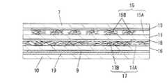
図5は本発明の第2の実施の形態によるタッチパネルの断面図、図6は同分解斜視図であり、同図において、フィルム状で光透過性の上基板11上面に、光透過性で略帯状の複数の上導電層15が、前後方向に配列形成されていることは実施の形態1の場合と同様であるが、この上導電層15は、厚さ0.1〜20μm前後のアクリル等の紫外線硬化樹脂15A内に、直径10〜100nm前後で長さ1〜15μm前後の銀等の複数の導電金属細線15Bが、所定箇所に分散されて形成されている。 FIG. 5 is a cross-sectional view of a touch panel according to a second embodiment of the present invention, and FIG. 6 is an exploded perspective view of the touch panel. In FIG. The plurality of strip-like upper
そして、13は一端が上導電層15端部に連結され、他端が上基板11外周右端に延出する上電極で、厚さ20nm〜10μm前後の銅箔から形成されると共に、複数の上電極13が上導電層15とは直交方向の左右方向に延出形成されている。
また、16は上基板11と同様のフィルム状で光透過性の下基板、17は上導電層15と同様に、紫外線硬化樹脂17A内に複数の導電金属細線17Bが分散された下導電層で、光透過性で略帯状の複数の下導電層17が下基板16上面に、上導電層15とは直交方向の左右方向に配列形成されている。
さらに、18は上電極13と同様に銅箔から形成された下電極で、一端が下導電層17端部に連結され他端が外周右端に延出する複数の下電極18が、下導電層17と平行方向の左右方向に延出形成されている。 Further, 18 is a lower electrode made of copper foil as in the case of the
そして、この複数の上導電層15と下導電層17は、実施の形態1の場合と同様に、複数の方形部が帯状に連結されて形成されると共に、これらの間には、略方形の複数の空隙部が設けられ、上基板11と下基板16が積重された状態では、各々の方形部が各々の空隙部に上下で交互に重なるように形成されている。 The plurality of upper
なお、上面全面に上導電層15や下導電層17と同様の光透過性のベース導電層19が形成されると共に、このベース導電層19前後端部から外周右端に延出する、略コの字状のベース電極9が形成されたベース基板10上面に、下基板16と上基板11、カバー基板7が重ねられ、これらが各々貼り合わされてタッチパネルが構成されていることは、実施の形態1の場合と同様である。 A light-transmitting base
つまり、本実施の形態においては、前後方向に配列形成された複数の上導電層15と、これとは直交方向の左右方向に配列形成された下導電層17が、導電金属細線15Bや17Bを分散した紫外線硬化樹脂15Aや17Aから形成され、これらが上基板11を介して所定の間隙を空けて対向配置されると共に、上導電層15から延出する上電極13も、下導電層17から延出する下電極18も銅箔で形成された構成となっている。 That is, in the present embodiment, the plurality of upper
なお、このようなタッチパネルの例えば上基板11を製作するには、図7(a)の部分断面図に示すように、先ず、紫外線硬化樹脂15A内全体に複数の導電金属細線15Bが分散された薄膜と、銅箔13Aが上面全面に積層された上基板11に、図7(b)に示すように、フォトレジスト法等によって露光・現像し、銅箔13A上面をドライフィルム等の絶縁樹脂製の被膜21でマスキングして、上導電層15のパターンとなる箇所を覆う。 In order to manufacture the
そして、次に、これを過硫酸アンモニウム希釈水溶液等のエッチング液に浸漬して、不要な箇所の銅箔13Aのみを溶融除去した後、リン酸と硝酸混合の希釈水溶液等のエッチング液に浸漬し、この下方の紫外線硬化樹脂15A内の導電金属細線15Bを溶融除去して、図7(c)に示すような、紫外線硬化樹脂15A内に複数の導電金属細線15Bが所定方向に配列され、この上に銅箔13Aが形成された上基板11を作製する。 Then, after immersing this in an etching solution such as an ammonium persulfate diluted aqueous solution and melting and removing only the
さらに、この後、図7(d)に示すように、所定の銅箔13A上面に被膜21によって露光・現像してマスキングを行い、過硫酸アンモニウム希釈水溶液等のエッチング液に浸漬して、不要な箇所の銅箔13Aを溶融除去し、図7(e)に示すような、紫外線硬化樹脂15A内の導電金属細線15Bによって所定方向に配列された複数の上導電層15と、これから延出する複数の上電極13が形成された上基板11が完成する。 Then, as shown in FIG. 7 (d), the upper surface of the
そして、このように構成されたタッチパネルが、液晶表示素子等の表示素子の前面に配置されて電子機器に装着されると共に、外周右端に延出した複数の上電極13や下電極18、ベース電極9がフレキシブル配線板やコネクタ(図示せず)等を介して、機器の電子回路(図示せず)に電気的に接続される。 The touch panel configured in this manner is disposed on the front surface of a display element such as a liquid crystal display element and is mounted on an electronic device, and a plurality of
以上の構成において、電子回路から複数の上電極13と下電極18へ順次電圧が印加された状態で、タッチパネル背面の表示素子の表示に応じて、カバー基板7上面を指等で触れて操作すると、この操作した箇所の上導電層15と下導電層17の間の静電容量が変化するため、これによって操作された箇所を電子回路が検出し、機器の様々な機能の切換えが行われる。 In the above configuration, when a voltage is sequentially applied from the electronic circuit to the plurality of
つまり、例えば複数のメニュー等が背面の表示素子に表示された状態で、所望のメニュー上のカバー基板7上面に指等を触れると、この指に電荷の一部が導電して、操作した箇所のタッチパネルの上導電層15と下導電層17の間の容量が変化し、これを電子回路が検出することによって、所望のメニューの選択等が行われるように構成されている。 That is, for example, when a finger or the like is touched on the upper surface of the
そして、このようなタッチパネルの上導電層15や下導電層17、ベース導電層19を、複数の導電金属細線15Bや17Bを分散した紫外線硬化樹脂15Aや17Aで形成することで、高価な酸化インジウム錫等の金属薄膜でこれらを形成する場合に比べ、安価にタッチパネルを構成できるようになっている。 Then, the upper
さらに、上導電層15や下導電層17をこのように形成することで、酸化インジウム錫等の金属薄膜でこれらを形成した場合に比べ、光の透過率も91〜92%と優れたものとなるため、タッチパネル背面の液晶表示素子等の表示も見易くなり、視認性が良好で操作の行い易いものとすることが可能となる。 Furthermore, by forming the upper
すなわち、上導電層15や下導電層17、ベース導電層19を比較的安価な、導電金属細線15Bや17Bを分散した紫外線硬化樹脂15Aや17Aで形成することによって、エッチング加工等によって比較的簡易に上導電層15や下導電層17を形成できると共に、安価で、確実な操作が可能なタッチパネルを得ることができるように構成されている。 That is, the upper
また、上導電層15や下導電層17から延出する複数の上電極13や下電極18を銅箔で形成し、にじみやかすれ等の生じ易いスクリーン印刷等ではなく、エッチングによって上電極13や下電極18を形成することで、線幅や線間が0.03〜0.05mm前後の、細線化や狭間隔化を図った上電極13や下電極18の形成が可能なようになっている。 Further, the
つまり、複数の上電極13や下電極18を銅箔で形成することによって、上電極13や下電極18の細線化や狭間隔化が行えるため、全体の小型化や操作領域の拡大が図れると共に、にじみやかすれ等のない状態で上電極13や下電極18を形成できるため、機器の電子回路との安定した接続が可能となり、確実な操作が行えるように構成されている。 That is, by forming a plurality of
なお、以上の説明では、上導電層15と下導電層17、ベース導電層19の全てを、導電金属細線15Bや17Bを分散した紫外線硬化樹脂15Aや17Aで形成した構成について説明したが、ベース基板10の上面全面に形成され、エッチング加工等によってこれを殆んど除去する必要のないベース導電層19は、スパッタ法等によって酸化インジウム錫や酸化錫等で形成してもよく、あるいは、上導電層15または下導電層17のいずれかのみを、導電金属細線を分散した紫外線硬化樹脂で形成しても、本発明の実施は可能である。 In the above description, the upper
また、以上の説明では、上電極13と下電極18の両方を銅箔で形成した構成について説明したが、下導電層17と平行方向の左右方向に延出形成され、上電極13に比べ線幅や線間隔にやや余裕のある下電極18は、スクリーン印刷等によって銀やカーボン等で形成し、上導電層15と直交方向に延出する上電極13のみを銅箔で形成すれば、タッチパネルをより安価なものとすることができる。 In the above description, the structure in which both the
このように本実施の形態によれば、上導電層15または下導電層17の少なくとも一方を、導電金属細線15Bや17Bを分散した紫外線硬化樹脂15Aや17Aで形成することによって、エッチング加工等により比較的簡易に上導電層15や下導電層17を形成できると共に、安価で、確実な操作が可能なタッチパネルを得ることができるものである。 As described above, according to the present embodiment, at least one of the upper
また、上導電層15から延出する複数の上電極13、または下導電層17から延出する複数の下電極18の少なくとも一方を銅箔で形成することによって、電極の細線化や狭間隔化を図り、全体の小型化や操作領域の拡大が図れると共に、電極のにじみやかすれ等を防ぎ、機器の電子回路との安定した接続が可能なものを得ることができる。 In addition, by forming at least one of the plurality of
なお、以上の説明では、上基板11下面に下基板4や16を貼付した構成について説明したが、上基板11と下基板4や16の上下を逆にし、下基板4や16下面に上基板11を貼付した構成や、あるいは、下基板4や16に代えて、上基板11の上下面に上導電層12や15と下導電層5や17の両方を形成した構成としても、本発明の実施は可能である。 In the above description, the structure in which the
本発明によるタッチパネルは、安価で、確実な操作が可能なものを得ることができるという有利な効果を有し、主に各種電子機器の操作用として有用である。 The touch panel according to the present invention has an advantageous effect that an inexpensive and capable of reliable operation can be obtained, and is mainly useful for operation of various electronic devices.
4 下基板
5 下導電層
6 下電極
7 カバー基板
8 ベース導電層
9 ベース電極
10 ベース基板
11 上基板
12 上導電層
12A 薄膜
13 上電極
13A 銅箔
15 上導電層
15A、17A 紫外線硬化樹脂
15B、17B 導電金属細線
16 下基板
17 下導電層
18 下電極
19 ベース導電層
21 被膜4
Claims (2)
Translated fromJapanesePriority Applications (4)
| Application Number | Priority Date | Filing Date | Title |
|---|---|---|---|
| JP2010168891AJP2011146023A (en) | 2009-09-17 | 2010-07-28 | Touch panel |
| CN2010102849753ACN102023745B (en) | 2009-09-17 | 2010-09-16 | Touch panel |
| US12/883,722US20110063240A1 (en) | 2009-09-17 | 2010-09-16 | Touch panel |
| KR1020100090925AKR101153128B1 (en) | 2009-09-17 | 2010-09-16 | Touch panel |
Applications Claiming Priority (5)
| Application Number | Priority Date | Filing Date | Title |
|---|---|---|---|
| JP2009215346 | 2009-09-17 | ||
| JP2009215346 | 2009-09-17 | ||
| JP2009286128 | 2009-12-17 | ||
| JP2009286128 | 2009-12-17 | ||
| JP2010168891AJP2011146023A (en) | 2009-09-17 | 2010-07-28 | Touch panel |
Publications (2)
| Publication Number | Publication Date |
|---|---|
| JP2011146023Atrue JP2011146023A (en) | 2011-07-28 |
| JP2011146023A5 JP2011146023A5 (en) | 2013-09-05 |
Family
ID=43730035
Family Applications (1)
| Application Number | Title | Priority Date | Filing Date |
|---|---|---|---|
| JP2010168891APendingJP2011146023A (en) | 2009-09-17 | 2010-07-28 | Touch panel |
Country Status (4)
| Country | Link |
|---|---|
| US (1) | US20110063240A1 (en) |
| JP (1) | JP2011146023A (en) |
| KR (1) | KR101153128B1 (en) |
| CN (1) | CN102023745B (en) |
Families Citing this family (12)
| Publication number | Priority date | Publication date | Assignee | Title |
|---|---|---|---|---|
| TWI471790B (en)* | 2010-02-03 | 2015-02-01 | Wintek Corp | Capacitive touch sensor and its fabrication method and capacitive touch panel |
| JP2013122745A (en)* | 2011-11-11 | 2013-06-20 | Panasonic Corp | Touch panel and manufacturing method thereof |
| CN103197785B (en)* | 2012-01-06 | 2016-07-06 | 宸鸿科技(厦门)有限公司 | Contact panel and preparation method thereof |
| US20130221991A1 (en)* | 2012-02-29 | 2013-08-29 | Touchsensor Technologies, Llc | User interface having universal sensing electrode structure |
| GB2520793B (en) | 2012-03-02 | 2016-11-02 | Novalia Ltd | Touch-sensitive input device |
| GB2499987B (en) | 2012-03-02 | 2017-01-11 | Novalia Ltd | Touch-sensitive input device |
| CN103384451A (en)* | 2012-05-04 | 2013-11-06 | 群康科技(深圳)有限公司 | Manufacturing method for touch panel edge wire routing, touch panel and touch display device |
| TWI571912B (en)* | 2012-05-04 | 2017-02-21 | 群康科技(深圳)有限公司 | Method for making narrow electric wires on the peripheral region of touch screen, the touch screen containing the said wires, and display screen apparatus |
| JP2013235471A (en)* | 2012-05-10 | 2013-11-21 | Panasonic Corp | Touch panel |
| US20140104185A1 (en)* | 2012-10-15 | 2014-04-17 | Htc Corporation | Touch display device and handheld electronic device |
| JP6074871B2 (en)* | 2013-08-30 | 2017-02-08 | パナソニックIpマネジメント株式会社 | Display device with touch sensor, touch sensor, and method of manufacturing display device with touch sensor |
| KR102005504B1 (en) | 2017-06-28 | 2019-10-08 | 주식회사 한화 | Apparatus and Method for measuring pose based on augmented reality |
Citations (6)
| Publication number | Priority date | Publication date | Assignee | Title |
|---|---|---|---|---|
| JP2007200177A (en)* | 2006-01-30 | 2007-08-09 | Optrex Corp | Electronic device |
| JP2008009553A (en)* | 2006-06-27 | 2008-01-17 | Optrex Corp | Electrode substrate |
| JP2008077332A (en)* | 2006-09-20 | 2008-04-03 | Sharp Corp | Touch panel manufacturing method, touch panel, and electronic device |
| JP2008129708A (en)* | 2006-11-17 | 2008-06-05 | Alps Electric Co Ltd | Transparent touch panel and its manufacturing method |
| WO2009060717A1 (en)* | 2007-11-07 | 2009-05-14 | Konica Minolta Holdings, Inc. | Transparent electrode and method for producing transparent electrode |
| JP2009176198A (en)* | 2008-01-28 | 2009-08-06 | Hitachi Displays Ltd | Display device with touch panel |
Family Cites Families (19)
| Publication number | Priority date | Publication date | Assignee | Title |
|---|---|---|---|---|
| JP2003280819A (en) | 2002-03-20 | 2003-10-02 | Kawaguchiko Seimitsu Co Ltd | Method for manufacturing touch panel |
| JPWO2006018982A1 (en)* | 2004-08-19 | 2008-05-08 | 株式会社ブリヂストン | Information display device |
| JP2007012853A (en)* | 2005-06-30 | 2007-01-18 | Fujifilm Holdings Corp | Image reader |
| JP2007018226A (en)* | 2005-07-07 | 2007-01-25 | Three M Innovative Properties Co | Touch panel sensor |
| US20070063876A1 (en)* | 2005-08-24 | 2007-03-22 | Wong Alex K | Multiple sensing element touch sensor |
| US7932898B2 (en)* | 2005-09-20 | 2011-04-26 | Atmel Corporation | Touch sensitive screen |
| JP4779681B2 (en)* | 2006-02-07 | 2011-09-28 | パナソニック株式会社 | Touch panel |
| US8803813B2 (en)* | 2006-05-10 | 2014-08-12 | Cypress Semiconductor Corporation | Sensing device |
| JP4687559B2 (en)* | 2006-05-16 | 2011-05-25 | パナソニック株式会社 | Touch panel |
| JP2008017433A (en)* | 2006-07-05 | 2008-01-24 | Taiyo Yuden Co Ltd | Piezoelectric electroacoustic transducer |
| US9710095B2 (en)* | 2007-01-05 | 2017-07-18 | Apple Inc. | Touch screen stack-ups |
| WO2008093975A1 (en)* | 2007-02-02 | 2008-08-07 | Ampnt Inc. | Touch panel having closed loop electrode for equipotential build-up and manufacturing method thereof |
| JP2009093397A (en)* | 2007-10-09 | 2009-04-30 | Panasonic Corp | Touch panel and input device using the same |
| US20090140987A1 (en)* | 2007-12-04 | 2009-06-04 | Kai-Ti Yang | Duplex touch panel |
| JP2009170194A (en)* | 2008-01-15 | 2009-07-30 | Panasonic Corp | Touch panel and movable contact body and switch using the same |
| JP2009170195A (en)* | 2008-01-15 | 2009-07-30 | Panasonic Corp | Movable contact body and switch using the same |
| US8119937B2 (en)* | 2008-03-10 | 2012-02-21 | Young Fast Optoelectronics Co., Ltd. | Capacitive touch panel |
| US8508492B2 (en)* | 2009-01-19 | 2013-08-13 | Panasonic Corporation | Touch panel and method of detecting press operation position thereon |
| KR100909265B1 (en) | 2009-02-23 | 2009-07-27 | (주)이엔에이치테크 | Manufacturing method of capacitive touch screen panel |
- 2010
- 2010-07-28JPJP2010168891Apatent/JP2011146023A/enactivePending
- 2010-09-16KRKR1020100090925Apatent/KR101153128B1/ennot_activeExpired - Fee Related
- 2010-09-16USUS12/883,722patent/US20110063240A1/ennot_activeAbandoned
- 2010-09-16CNCN2010102849753Apatent/CN102023745B/enactiveActive
Patent Citations (6)
| Publication number | Priority date | Publication date | Assignee | Title |
|---|---|---|---|---|
| JP2007200177A (en)* | 2006-01-30 | 2007-08-09 | Optrex Corp | Electronic device |
| JP2008009553A (en)* | 2006-06-27 | 2008-01-17 | Optrex Corp | Electrode substrate |
| JP2008077332A (en)* | 2006-09-20 | 2008-04-03 | Sharp Corp | Touch panel manufacturing method, touch panel, and electronic device |
| JP2008129708A (en)* | 2006-11-17 | 2008-06-05 | Alps Electric Co Ltd | Transparent touch panel and its manufacturing method |
| WO2009060717A1 (en)* | 2007-11-07 | 2009-05-14 | Konica Minolta Holdings, Inc. | Transparent electrode and method for producing transparent electrode |
| JP2009176198A (en)* | 2008-01-28 | 2009-08-06 | Hitachi Displays Ltd | Display device with touch panel |
Also Published As
| Publication number | Publication date |
|---|---|
| CN102023745A (en) | 2011-04-20 |
| US20110063240A1 (en) | 2011-03-17 |
| KR101153128B1 (en) | 2012-06-04 |
| CN102023745B (en) | 2013-08-07 |
| KR20110030390A (en) | 2011-03-23 |
Similar Documents
| Publication | Publication Date | Title |
|---|---|---|
| JP2011146023A (en) | Touch panel | |
| TWI653567B (en) | Touch window and touch device including the same | |
| US9217890B2 (en) | Touch screen panel and method for manufacturing the same | |
| JP2012174003A (en) | Touch panel | |
| JP5407599B2 (en) | Touch panel | |
| SG176592A1 (en) | Electrostatic capacitance type input device | |
| JP5520162B2 (en) | Input device and manufacturing method thereof | |
| JP2008290354A (en) | Conductive sheet and manufacturing method thereof | |
| JP5892418B2 (en) | Touch panel sensor, touch panel sensor manufacturing method, and laminate for manufacturing touch panel sensor | |
| JP6576498B2 (en) | FPC integrated capacitance switch and method of manufacturing the same | |
| JP2014179063A (en) | Touch panel | |
| JP2011248667A (en) | Capacitance sensor | |
| JP2014029682A (en) | Touch panel | |
| JP2014026496A (en) | Touch panel | |
| JP2012150580A (en) | Touch panel | |
| JP5617570B2 (en) | Touch panel | |
| JP6405298B2 (en) | Capacitance type sensor, touch panel and electronic equipment | |
| JP2013050778A (en) | Touch panel | |
| JP6676450B2 (en) | Touch sensor and touch sensor manufacturing method | |
| JP2014112356A (en) | Touch panel | |
| JP2015069634A (en) | Touch panel and method of manufacturing the same | |
| JP2013012019A (en) | Touch panel | |
| JP2015069609A (en) | Touch panel | |
| JP6242710B2 (en) | Manufacturing method of input device | |
| JP2014035615A (en) | Touch panel |
Legal Events
| Date | Code | Title | Description |
|---|---|---|---|
| A521 | Written amendment | Free format text:JAPANESE INTERMEDIATE CODE: A523 Effective date:20130724 | |
| A621 | Written request for application examination | Free format text:JAPANESE INTERMEDIATE CODE: A621 Effective date:20130724 | |
| RD01 | Notification of change of attorney | Free format text:JAPANESE INTERMEDIATE CODE: A7421 Effective date:20130807 | |
| A131 | Notification of reasons for refusal | Free format text:JAPANESE INTERMEDIATE CODE: A131 Effective date:20131217 | |
| A977 | Report on retrieval | Free format text:JAPANESE INTERMEDIATE CODE: A971007 Effective date:20131218 | |
| RD01 | Notification of change of attorney | Free format text:JAPANESE INTERMEDIATE CODE: A7421 Effective date:20140108 | |
| A521 | Written amendment | Free format text:JAPANESE INTERMEDIATE CODE: A523 Effective date:20140213 | |
| A131 | Notification of reasons for refusal | Free format text:JAPANESE INTERMEDIATE CODE: A131 Effective date:20140325 | |
| RD01 | Notification of change of attorney | Free format text:JAPANESE INTERMEDIATE CODE: A7421 Effective date:20140417 | |
| A02 | Decision of refusal | Free format text:JAPANESE INTERMEDIATE CODE: A02 Effective date:20140826 |