JP2011141464A - Liquid crystal display system integrated with touch detector - Google Patents
Liquid crystal display system integrated with touch detectorDownload PDFInfo
- Publication number
- JP2011141464A JP2011141464AJP2010002586AJP2010002586AJP2011141464AJP 2011141464 AJP2011141464 AJP 2011141464AJP 2010002586 AJP2010002586 AJP 2010002586AJP 2010002586 AJP2010002586 AJP 2010002586AJP 2011141464 AJP2011141464 AJP 2011141464A
- Authority
- JP
- Japan
- Prior art keywords
- liquid crystal
- electrode
- display
- crystal display
- function
- Prior art date
- Legal status (The legal status is an assumption and is not a legal conclusion. Google has not performed a legal analysis and makes no representation as to the accuracy of the status listed.)
- Pending
Links
- 239000004973liquid crystal related substanceSubstances0.000titleclaimsabstractdescription72
- 238000000034methodMethods0.000claimsabstractdescription19
- 238000001514detection methodMethods0.000claimsdescription54
- 239000000758substrateSubstances0.000claimsdescription32
- 230000005540biological transmissionEffects0.000claimsdescription8
- 230000031700light absorptionEffects0.000claimsdescription6
- 230000035945sensitivityEffects0.000claimsdescription4
- 238000013459approachMethods0.000claimsdescription3
- 239000002356single layerSubstances0.000claimsdescription2
- 238000004519manufacturing processMethods0.000abstractdescription7
- 238000010521absorption reactionMethods0.000abstractdescription3
- 238000010586diagramMethods0.000description6
- 238000003491arrayMethods0.000description5
- 239000010410layerSubstances0.000description5
- 239000011521glassSubstances0.000description3
- 238000007747platingMethods0.000description2
- 239000003086colorantSubstances0.000description1
- 238000007796conventional methodMethods0.000description1
- 230000009977dual effectEffects0.000description1
- 230000000694effectsEffects0.000description1
- 230000036571hydrationEffects0.000description1
- 238000006703hydration reactionMethods0.000description1
- 230000004048modificationEffects0.000description1
- 238000012986modificationMethods0.000description1
- 230000001360synchronised effectEffects0.000description1
Images


Landscapes
- Liquid Crystal (AREA)
- Devices For Indicating Variable Information By Combining Individual Elements (AREA)
- Liquid Crystal Display Device Control (AREA)
- Control Of Indicators Other Than Cathode Ray Tubes (AREA)
Abstract
Description
Translated fromJapanese本発明は、液晶表示(LCD)パネルに用いる容量タッチセンサに関する。特に、液晶表示パネルの表示電極を利用し、容量タッチ検出器のセンサ電極とし、別途電極の追加が不要であるタッチ検出器と統合された液晶表示システムに関する。 The present invention relates to a capacitive touch sensor used for a liquid crystal display (LCD) panel. In particular, the present invention relates to a liquid crystal display system that uses display electrodes of a liquid crystal display panel as sensor electrodes of a capacitive touch detector and is integrated with a touch detector that does not require additional electrodes.
タッチパネルは、既に多くの電子製品の入力部材に広く応用されている。特に、タッチパネル検出機能を有する液晶パネルは、タッチパネルを液晶表面に付加して得られる。この技術を用いる従来技術は、例えば、Ming-shen Sunの米国特許第6538706B2号明細書、Yong Ik Bang等の米国特許第7557869B2号明細書、Yun Cheol Jeong等の米国特許第7508461B2号明細書がある。タッチパネルを液晶表示パネルに付加することは、タッチパネルを液晶表示パネル上に付属部材として加えることである。コストを増加する以外に、この技術は、パネル全体の厚さ及び重量を増加させ、より多くの光が吸収及び反射するという欠点を招く。 Touch panels have already been widely applied to input members of many electronic products. In particular, a liquid crystal panel having a touch panel detection function is obtained by adding a touch panel to the liquid crystal surface. Prior art using this technique includes, for example, US Pat. No. 6,538,706B2 to Ming-shen Sun, US Pat. No. 7,557,869B2 to Yong Ik Bang et al., US Pat. No. 7,508,461 B2 to Yun Cheol Jeong et al. . Adding the touch panel to the liquid crystal display panel means adding the touch panel as an accessory member on the liquid crystal display panel. In addition to increasing costs, this technique increases the overall thickness and weight of the panel, resulting in the disadvantage of more light being absorbed and reflected.
前記の従来技術は、抵抗型タッチパネルである。抵抗型タッチパネルは、2層の電極を有する。タッチパネル内の多層の電極が余計な光の吸収及び反射を招き、液晶表示パネルの性能が低下する。中国特許第ZL200620013292.3号で使用する技術は、前記の欠点を解決することができる。この技術中、一層の透明導電膜は、液晶表示パネルの上ガラス基板上に直接、タッチセンサ電極として鍍金される。この従来技術は、容量型タッチセンサであり、且つただ一層の導電膜で抵抗型タッチセンサの2層の導電膜に置き換えることのみ必要である。 The prior art is a resistive touch panel. The resistive touch panel has two layers of electrodes. The multilayer electrodes in the touch panel cause extra light absorption and reflection, and the performance of the liquid crystal display panel deteriorates. The technique used in Chinese Patent No. ZL200620013292.3 can solve the above-mentioned drawbacks. In this technique, a single transparent conductive film is plated directly on the upper glass substrate of the liquid crystal display panel as a touch sensor electrode. This prior art is a capacitive touch sensor, and it is only necessary to replace the two-layer conductive film of the resistive touch sensor with a single conductive film.
この従来技術は、液晶表示パネルの厚さ及び重量を減少することができるが、透明導電膜は、依然として光が吸収、反射され、製造コストがタッチセンサの従来のLCDパネルより高い。タッチセンサ電極は、液晶表示パネルの上ガラス基板内に嵌め込み、余計な光の吸収、反射を回避することが好ましい。 Although this prior art can reduce the thickness and weight of the liquid crystal display panel, the transparent conductive film still absorbs and reflects light, and the manufacturing cost is higher than the conventional LCD panel of touch sensor. It is preferable that the touch sensor electrode is fitted into the upper glass substrate of the liquid crystal display panel to avoid unnecessary absorption and reflection of light.
液晶表示パネル及び抵抗型タッチセンサパネルを統合する技術は、Mikio Kurihara等の米国特許第6,501,529B1号明細書に開示されている。その構造は、2片の基板、第1基板及び第2基板を有する。液晶は、2片の基板間に注入されている。各基板の上において、1つの表示イメージを提供する表示電極及び1つのタッチセンサ電極にタッチ位置を検出させる。この構造は、パネル全体の厚さ及び重量を減少する。また、光の吸収及び反射も減少される。但し、タッチパネルセンサ電極の位置が制限され、なぜならば、タッチセンサ電極及び表示電極が重なり合うことができないからである。もう1つの欠点は、表示電極の構造及びタッチセンサ電極の構造が異なり、且つ製造コストが比較的高いことである。 A technique for integrating a liquid crystal display panel and a resistive touch sensor panel is disclosed in US Pat. No. 6,501,529 B1 of Mikio Kurihara et al. The structure has two pieces of substrate, a first substrate and a second substrate. Liquid crystal is injected between the two substrates. On each substrate, a touch position is detected by a display electrode that provides one display image and a touch sensor electrode. This structure reduces the overall thickness and weight of the panel. Also, light absorption and reflection is reduced. However, the position of the touch panel sensor electrode is limited because the touch sensor electrode and the display electrode cannot overlap. Another disadvantage is that the structure of the display electrode and the structure of the touch sensor electrode are different and the manufacturing cost is relatively high.
低コストで、軽薄で高品質であることは、多くのタッチパネル及び液晶表示パネルの結合の応用において、重要である。上記効果を得る為、好適な方法は、液晶表示電極をタッチセンサ電極として利用し、余計な構造を増加しないことである。 Low cost, light weight and high quality are important in many touch panel and liquid crystal display panel applications. In order to acquire the said effect, a suitable method is using a liquid crystal display electrode as a touch sensor electrode, and not increasing an extra structure.
図1は、従来のタッチセンサ機能を有さない液晶表示装置の断面図である。図1において、この装置は、2つのガラス基板、1片上基板11及び1片の下基板12を含む。上表示電極130,131,132,133は、上基板11に鍍金され、下表示電極14は、下基板12に鍍金される。各上表示電極と下表示電極14は、1つの画素(pixel or segment)を形成する。一層の液晶(層)15が上基板11及び下基板12の間に注入される。この液晶表示パネルは、下偏光片(polarizer)17及び上偏光片16及びバックライド(back light)18を含む。 FIG. 1 is a cross-sectional view of a conventional liquid crystal display device having no touch sensor function. In FIG. 1, the apparatus includes two glass substrates, a single piece
図1において、上基板11及び下基板12の間の距離が小さいので上表示電極130,131,132,133及び下表示電極14の間の容量が大きくなる。直接上表示電極を利用し、タッチセンサ電極として利用すれば、感度が低下し、正確な検出を行なうことが困難である。表示機能を実行時、交流電圧波形は、2つの電極に加える必要がある。同一上表示電極は、タッチセンサとして用いられる場合、タッチセンサの検出は、交流電圧波形により影響を受ける。この問題を解決する為、表示機能及びタッチ機能間のマルチプレキシング(multiplexing)方式を用いて解決する必要がある。 In FIG. 1, since the distance between the
本発明の目的は、タッチ検出機能を有する液晶表示パネルを提供することにある。 An object of the present invention is to provide a liquid crystal display panel having a touch detection function.
本発明のもう1つの目的は、タッチ検出機能を有さない液晶表示パネルと同一工程で製造するタッチ検出機能を有する液晶表示パネルを提供することにある。 Another object of the present invention is to provide a liquid crystal display panel having a touch detection function manufactured in the same process as a liquid crystal display panel having no touch detection function.
本発明のもう1つの目的は、タッチセンサが余計な光の吸収、反射を招くことのないタッチ検出機能を有する液晶表示パネルを提供することにある。 Another object of the present invention is to provide a liquid crystal display panel having a touch detection function that does not cause excessive absorption and reflection of light by the touch sensor.
本発明のもう1つの目的は、表示機能のタッチセンサに対する干渉が最も低いタッチ検出機能を有する液晶表示パネルを提供することにある。 Another object of the present invention is to provide a liquid crystal display panel having a touch detection function with the lowest interference with the touch sensor of the display function.
上記の目的を達成するため、本発明の第1観点は、透明型タッチセンサ及び液晶表示を統合したシステムを開示することにあり、透明型液晶パネル及び制御システムを含み、液晶表示パネルは、上基板と、下基板と、上電極アレイと、下電極アレイと、上偏光片と、下偏光片と、液晶と、背光板と、を含む。制御システムは、マイクロプロセッサと、表示制御回路と、表示駆動回路アレイと、タッチ検出回路と、該上電極を対応する下電極に短絡する伝送ゲートアレイと、を含む。タッチ検出回路は、物体又は手指の電極への接近を検出することに用いられる。表示制御回路及び表示駆動回路は、表示機能を実行することに用いる。そのうち、改良した箇所は、以下である。一対の電極は、上電極アレイの1つの上電極と下電極アレイの1つの下電極を含み、液晶表示パネルで1つの画素を表示することに用い、同一対の電極は、タッチ検出機能を実行することに用いることもできる。表示機能及びタッチ検出機能は、時間マルチプレキシング技術により実行する。表示機能を実行時、上電極及び下電極は、表示制御回路から表示駆動回路の波形発生器に接続する。タッチ機能を実行時、上電極及び下電極及び表示制御回路は、相互に接続しない。一対の電極の上電極及び下電極が短絡され、その機能が単一タッチセンサ電極となる。上電極及び下電極の容量が短絡されれば、タッチ検出機能の感度に対して負荷の影響を及ぼさない。タッチ検出機能を操作する時、上電極及び下電極及び表示駆動回路の波形発生器は、接続しないので、表示駆動回路は、タッチ検出機能に対して干渉を形成しない。本発明は、工程を追加する必要がなく、且つタッチ検出機能を加えることにより光の吸収、反射を増加させることがない。 In order to achieve the above object, a first aspect of the present invention is to disclose a system in which a transparent touch sensor and a liquid crystal display are integrated, and includes a transparent liquid crystal panel and a control system. A substrate, a lower substrate, an upper electrode array, a lower electrode array, an upper polarizing piece, a lower polarizing piece, a liquid crystal, and a back plate are included. The control system includes a microprocessor, a display control circuit, a display drive circuit array, a touch detection circuit, and a transmission gate array that shorts the upper electrode to a corresponding lower electrode. The touch detection circuit is used to detect the approach of an object or finger to the electrode. The display control circuit and the display driving circuit are used to execute a display function. Among them, the improved parts are as follows. The pair of electrodes includes one upper electrode of the upper electrode array and one lower electrode of the lower electrode array, and is used to display one pixel on the liquid crystal display panel. The same pair of electrodes performs a touch detection function. It can also be used to do. The display function and the touch detection function are executed by a time multiplexing technique. When executing the display function, the upper electrode and the lower electrode are connected from the display control circuit to the waveform generator of the display drive circuit. When executing the touch function, the upper electrode, the lower electrode, and the display control circuit are not connected to each other. The upper electrode and the lower electrode of the pair of electrodes are short-circuited, and the function becomes a single touch sensor electrode. If the capacities of the upper electrode and the lower electrode are short-circuited, there is no influence of the load on the sensitivity of the touch detection function. When operating the touch detection function, the upper and lower electrodes and the waveform generator of the display drive circuit are not connected, so the display drive circuit does not form interference with the touch detection function. The present invention does not require additional steps and does not increase light absorption or reflection by adding a touch detection function.
本発明の他の観点は、タッチ検出及び液晶表示を統合したシステムを開示することにあり、そのうち、液晶表示システムが反射型であり、且つ背光板が一層の反射板で置き換え、下偏光片を有さない。 Another aspect of the present invention is to disclose a system in which touch detection and liquid crystal display are integrated, in which the liquid crystal display system is a reflection type, and the back plate is replaced with a single reflection plate, and the lower polarizing piece is replaced. I don't have it.
本発明の更に他の観点は、タッチ検出及び液晶表示を統合したシステムを開示することにあり、そのうち、液晶表示システムは、混合型液晶表示システムであり、表示電極は、タッチ機能を有する、及びタッチ機能を有さない2種の表示電極から構成することもできる。タッチ検出機能を有さない領域は、下電極を共用することができ、タッチ検出機能を有する領域は、電極対(electrode pair)を使用する。 Still another aspect of the present invention is to disclose a system that integrates touch detection and liquid crystal display, in which the liquid crystal display system is a mixed liquid crystal display system, the display electrode has a touch function, and It can also be composed of two types of display electrodes that do not have a touch function. The region having no touch detection function can share the lower electrode, and the region having the touch detection function uses an electrode pair.
本発明は、タッチ検出機能を有する液晶表示パネルを提供する。 The present invention provides a liquid crystal display panel having a touch detection function.
本発明は、タッチ検出機能を有さない液晶表示パネルと同一工程で製造するタッチ検出機能を有する液晶表示パネルを提供する。 The present invention provides a liquid crystal display panel having a touch detection function manufactured in the same process as a liquid crystal display panel having no touch detection function.
本発明は、タッチセンサが余計な光の吸収、反射を招くことのないタッチ検出機能を有する液晶表示パネルを提供する。 The present invention provides a liquid crystal display panel having a touch detection function in which a touch sensor does not cause extra light absorption and reflection.
本発明は、表示機能のタッチセンサに対する干渉が最も低いタッチ検出機能を有する液晶表示パネルを提供する。 The present invention provides a liquid crystal display panel having a touch detection function with the lowest interference with a touch sensor having a display function.
本発明の上記及びその他の目的及び利点を分かり易くする為、以下の図面及び好適実施例を参考にして説明する。 In order to make the aforementioned and other objects and advantages of the present invention comprehensible, a description will be given with reference to the following drawings and preferred embodiments.
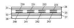
図2は、本発明を用いることができる透明型液晶表示(LCD)パネルである。
図2に示す液晶表示パネルは、2片の基板、上基板21及び下基板22を有する。2片の基板の間に液晶25を注入する。上表示電極アレイ230,231,232,233は、上基板21上に鍍金される。下表示電極アレイ240,241,242,243は、下基板22上に鍍金される。上表示電極の1つ230及び相応する下表示電極240は、液晶表示パネルの1つの画素(pixel)を表示することに用いる。上基板21の下に上偏光片26を有し、下基板22の上に下偏光片27を有する。背光板28は、下偏光片27の下に位置する。FIG. 2 is a transparent liquid crystal display (LCD) panel in which the present invention can be used.
The liquid crystal display panel shown in FIG. 2 has two substrates, an
図3は、本発明を用いることができる反射型液晶表示(LCD)パネルである。反射型液晶表示パネルの構造及び透明型液晶表示パネルと相似する。但し、反射型液晶表示パネルは、下偏光片を有さず、背光板は、反射板38で置き換えられる。本発明は、反射型及び透明型液晶表示パネルに応用することができ、回路の修正が必要ない。 FIG. 3 is a reflective liquid crystal display (LCD) panel in which the present invention can be used. The structure of the reflective liquid crystal display panel is similar to that of the transparent liquid crystal display panel. However, the reflective liquid crystal display panel does not have the lower polarizing piece, and the back plate is replaced with the
本発明の目的は、同一の電極により表示機能の電極及びタッチ機能の電極をさせることにある。上記の目的を達成する為、表示機能の電極及びタッチ機能の電極の間で時間マルチプレキシング(time multiplexing)技術を使用することができる。 An object of the present invention is to provide a display function electrode and a touch function electrode by the same electrode. In order to achieve the above object, a time multiplexing technique can be used between the display function electrode and the touch function electrode.
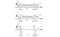
表示機能の電極及びタッチ機能の電極の間に使用する時間マルチプレキシング技術は、図4の波形を用いて説明できる。図4の上,下電極間に印加する電圧の波形41,42,43及び図2、図3の電極は相対する。波形41は、上電極に印加する電圧であり、波形42は、下電極に印加する電圧であり、波形43は、上電極及び下電極に印加する相対電圧である。 The time multiplexing technique used between the display function electrode and the touch function electrode can be described using the waveforms of FIG. The
図4に示すように、2種の時間間隔T1,T2を有する。時間T1時、システムは、表示機能を実行する。時間T2時、システムは、タッチ機能を実行する。 As shown in FIG. 4, there are two types of time intervals T1 and T2. At time T1, the system performs a display function. At time T2, the system executes the touch function.
時間T1時、上電極及び下電極がLCD表示駆動回路に接続する。この時間間隔時、タッチ検出プロセスを実行できず、なぜならば、表示波形の干渉によりタッチ検出エラーを招くからである。 At time T1, the upper electrode and the lower electrode are connected to the LCD display driving circuit. During this time interval, the touch detection process cannot be performed because a touch detection error is caused by interference of display waveforms.
時間T2時、システムは、タッチ回路機能を実行し、上電極及び下電極は、タッチセンサとなる。表示回路の波形からの干渉を回避するため、上電極及び下電極は、表示駆動回路から切断する必要がある。上電極及び下電極は、何れもタッチ検出回路に接続する。また、時間T2時、各上電極及び相応する下電極は、短絡を形成し、この時間、この2つの電極は、同一の電圧を有し、図4の波形41,42のようになる。図4中、時間T2時、タッチ検出回路からの波形を合わせたものは、ここでは、方形波で表示するが、その他の波形であることもでき、タッチ検出回路により決定される。時間T2時にタッチ検出回路から上下電極までを合わせた電圧波形が何であるかを問わず、上下電極間の電圧が0であり、例えば、図4の波形43に示すようになる。且つ、タッチ検出回路からの波形を合わせたものは、LCDの表示品質に影響を及ぼさない。上電極及び相応する下電極間に大きな容量を有し、上下電極が同様に短絡され、上下電極が時間T2である時、その機能は、1つの電極のようになる。この容量のタッチセンサに対する負荷は0であり、タッチ検出回路の感度に影響を及ぼさない。 At time T2, the system performs a touch circuit function, and the upper and lower electrodes become touch sensors. In order to avoid interference from the waveform of the display circuit, it is necessary to disconnect the upper electrode and the lower electrode from the display drive circuit. Both the upper electrode and the lower electrode are connected to the touch detection circuit. Also, at time T2, each upper electrode and the corresponding lower electrode form a short circuit, and during this time, the two electrodes have the same voltage, as shown by
液晶表示パネルについて言えば、「ON」又は「OFF」状態を問わず、2つの表示電極間に印加する電圧は、如何なる直流成分も有さない交流電圧である必要がある。 Regarding the liquid crystal display panel, the voltage applied between the two display electrodes regardless of the “ON” or “OFF” state needs to be an AC voltage having no DC component.
図4に示す波形は、1つの映像点が「ON」状態にある時の対時間を説明する曲線図である。波形43は、上下電極間に印加される電圧である。この電圧は、直流成分を有さない交流電圧である。 The waveform shown in FIG. 4 is a curve diagram illustrating time versus time when one video point is in the “ON” state. A
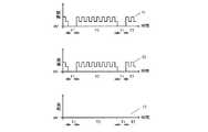
1つの映像点が「OFF」状態にあることを表示する為には、上下表示電極間の相対電圧値を小さくし、良好な対比品質を獲得しなければならない。簡単な解決方法は、表示時間T1時、上下電極に0電圧を印加することである。この波形は、図5に示す。図5中の波形51は、上電極に印加する電圧であり、波形52は、下電極に印加する電圧であり、波形53は、上下電極間に印加する電圧である。図5の波形53から分かるように、上下電極間の相対電圧が0である。従って、「ON」又は「OFF」状態の表示対比が十分に良好となる。 In order to display that one video point is in the “OFF” state, it is necessary to reduce the relative voltage value between the upper and lower display electrodes to obtain good contrast quality. A simple solution is to apply 0 voltage to the upper and lower electrodes at the display time T1. This waveform is shown in FIG. A
「OFF」状態において、表示時間T1時、上下電極間の電圧が0である必要がない。図6中、1つの0でない電圧が表示時間T1時、上電極及び下電極に印加される。この波形は、図6中の波形61は、上電極に印加する電圧であり、波形62は、下電極に印加する電圧であり、2つの電極が一様の波形を有し、2つの電極間の電圧が0であり、図6の波形63に示すようである。 In the “OFF” state, the voltage between the upper and lower electrodes does not have to be 0 at the display time T1. In FIG. 6, one non-zero voltage is applied to the upper electrode and the lower electrode at the display time T1. In this waveform, a
本発明は、タッチセンサ期間において、上電極が下電極と短絡する必要があり、上電極は、従来のLCDのように1つの共用下電極を共用することができない。この構造は、図2及び図3に詳細に記載する。 In the present invention, the upper electrode needs to be short-circuited with the lower electrode during the touch sensor period, and the upper electrode cannot share one common lower electrode as in a conventional LCD. This structure is described in detail in FIGS.
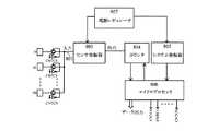
図7は、本発明の技術を示す回路図である。図7中、タッチセンサの液晶システム7は、マイクロプロセッサ71と、表示制御回路72と、タッチ検出回路73と、表示駆動回路アレイ740〜74Nと、伝送ゲートアレイ750〜75Nと、上電極アレイ770〜77Nと、下電極アレイ760〜76Nと、を含む。上電極と下電極を含む電極対は、表示機能として用いることも、手指又は物体がこの電極に接近することを検出することに用いることもできる。単一電極で上記2種の機能を行なうには、時間マルチプレキシング技術を使用することができる。マイクロプロセッサ71は、信号を発生し、2種の機能間で時間マルチプレキシングな命令を実行する。表示制御回路72は、制御信号を発生し、表示駆動回路に与える。表示駆動回路は、電極対が表示機能を実行するよう駆動することに用いる。タッチ検出回路73は、手指又は物体がこの電極に接近したことを検出することに用いる。表示時間T1の期間において、電極760,770は、表示制御回路72により制御され、表示駆動回路アレイ740の波形発生器に接続する。伝送ゲートアレイ750がオフとされ、且つタッチ検出回路73の入力バイアスが浮動する。この状態において、電極は、表示制御回路72の影響のみを受け、タッチ検出回路73の影響を受けない。 FIG. 7 is a circuit diagram showing the technique of the present invention. In FIG. 7, the touch sensor
タッチセンサ時間T2の期間において、電極760,770の機能は、タッチセンサであり、表示駆動回路(アレイ)740の波形発生器に接続しない。この時間において、伝送ゲートアレイ750がオンとなり、電極760,770を短絡させる。2つの電極の機能は、1つの電極のようであり、2つの電極間の容量がタッチセンサ機能の動作に対して影響を及ぼさない。表示駆動回路(アレイ)740は、電極に接続せず、且つ2つの電極間の容量がタッチセンサに影響を及ぼさないので、回路7は、タッチセンサの動作を正常に実行することができる。 In the period of the touch sensor time T2, the function of the
公開文献は、多種の容量式物体接近センサがある。大多数の容量式物体接近センサは、何れも本発明のタッチ検出回路となることができる。林緒徳(本発明の発明者)の米国特許第7023221B1号明細書、中華民国特許第I259908号明細書、欧州特許第1791260B1号明細書、中華人民共和国特許第ZL200510080231.9号明細書及び日本特許第4365817号明細書は、1種の容量式物体接近センサであり、本発明の接触センサ回路となることができる。本発明中、タッチ検出回路内において、一列N個センサのみ必要であり、この接触センサ回路は、図8に表示する。
この回路の動作の詳細は、米国特許第7023221B1号明細書に記載される。ここで、タッチ検出回路73の動作及びLCD表示機能間の動作を詳細に説明する。図8の回路は、図7のタッチ検出回路73に用いられる時、タッチ検出回路の動作は、図7のマイクロプロセッサ71により制御される。図8のマイクロプロセッサ806は、カウンタ804とシステム発信器805(電源レギュレータ807により電源供給)により駆動されるとともに、図7のマイクロプロセッサ71と結合して1つのマイクロプロセッサとなることができる。そうでなければ、マイクロプロセッサ806は、マイクロプロセッサ71と同期して動作し、タッチセンサ機能とLCD表示機能の同期動作を保証する必要がある。図7に示すように、下電極アレイ760,761・・・76Nは、それぞれタッチ検出回路73の入力I0,I1・・・INに接続する。タッチセンサ時間T2の期間、全ての電極が順に伝送ゲートCNTC0,CNTC1・・・CNTCNをスキャンし、図8に示すようになる。LCD表示時間T1の期間において、タッチ検出回路73の入力801は、図8の伝送ゲートCNTC0,CNTC1・・・CNTCNをオンとし、表示電極から切断される。図8中のセンサ発振器803内のバイアス回路は、LCD表示回路の動作に影響を及ぼさない。The published literature includes various types of capacitive object proximity sensors. Any of the majority of capacitive object proximity sensors can be the touch detection circuit of the present invention. US Pat. No. 7,022,221 B1, No. I 259908, No. I259908, No. EP 1791260 B1, No. ZL200510080231.9, and Japanese Patent No. 4,365,817. The specification is a kind of capacitive object proximity sensor and can be a contact sensor circuit of the present invention. In the present invention, only N sensors in a row are required in the touch detection circuit, and this contact sensor circuit is displayed in FIG.
Details of the operation of this circuit are described in US Pat. No. 7,022,221 B1. Here, the operation of the
本発明の技術の記載のように、本発明の液晶パネル及び従来の表示パネルの唯一異なる箇所は、下電極の構造である。本発明技術及び従来の技術の製造工程は相違がない。本発明の液晶表示パネルの製造は、コストを増加しない。同時に従来の表示パネルと比べて、本発明の表示パネルは、鍍金層を増加しない。表示パネルが鍍金層を増加しないことは、光の吸収、反射を増加しないことを意味する。 As described in the technology of the present invention, the only difference between the liquid crystal panel of the present invention and the conventional display panel is the structure of the lower electrode. There is no difference between the manufacturing process of the present invention technique and the conventional technique. The production of the liquid crystal display panel of the present invention does not increase the cost. At the same time, the display panel of the present invention does not increase the plating layer as compared with the conventional display panel. The fact that the display panel does not increase the plating layer means that light absorption and reflection are not increased.
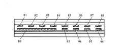
同様の製造工程を使用し、従来の表示パネル及び本発明の表示パネルを混合型として結合することができる。この混合型表示パネルは、図1及び図2の構造を結合して形成されることができ、図9に示すようになる。図9中、上電極85,86,87,88及び下電極95,96,97,98は、表示及びタッチの二重の機能を果たすことができる。上電極81,82,83,84及び共用下電極80は、表示電極としてのみ用いることができる。 Using the same manufacturing process, the conventional display panel and the display panel of the present invention can be combined as a mixed type. The mixed display panel can be formed by combining the structures shown in FIGS. 1 and 2 and is as shown in FIG. In FIG. 9, the
なお、本発明では好ましい実施例を前述の通り開示したが、これらは決して本発明に限定するものではなく、当該技術を熟知する者なら誰でも、本発明の精神と領域を脱しない均等の範囲内で各種の変動や潤色を加えることができることは勿論である。 In the present invention, the preferred embodiments have been disclosed as described above, but these are not intended to limit the present invention in any way, and anyone who is familiar with the technology can make an equivalent scope without departing from the spirit and scope of the present invention. Of course, various fluctuations and hydration colors can be added.
7 液晶表示システム
11 上基板
12 下基板
14 下表示電極
15 液晶
16 上偏光片
17 下偏光片
18 背光板
21 上基板
22 下基板
25 液晶
26 上偏光片
27 下偏光片
28 背光板
38 反射板
41 上電極に印加する電圧の波形
42 下電極に印加する電圧の波形
43 上下電極間に印加する電圧の波形
51 上電極に印加する電圧の波形
52 下電極に印加する電圧の波形
53 上下電極間に印加する電圧の波形
61 上電極に印加する電圧の波形
62 下電極に印加する電圧の波形
63 上下電極間に印加する電圧の波形
71 マイクロプロセッサ
72 表示制御回路
73 タッチ検出回路
80 共用下電極
81,82,83,84 上電極
85,86,87,88 上電極
95,96,97,98 下電極
130,131,132,133 上表示電極
230,231,232,233 上表示電極
240,241,242,243 下表示電極
740−74N 表示駆動回路アレイ
750−75N 伝送ゲートアレイ
760−76N 下電極アレイ
770−77N 上電極アレイ
801 入力
803 センサ発振器
804 カウンタ
805 システム発振器
806 マイクロプロセッサ
807 電源レギュレータ7 Liquid
Claims (3)
Translated fromJapanese一対の電極が該上電極アレイの1つの上電極と該下電極アレイの1つの下電極を含み、該液晶表示パネルで1つの画素を表示することに用い、同一対の電極がタッチ検出機能を実行することに用いることもできることと、
該表示機能及び該タッチ検出機能は、時間マルチプレキシング技術により実行されることと、
表示機能を実行時、該上電極及び該下電極は、該表示制御回路から該表示駆動回路の波形発生器に接続することと、
タッチ機能を実行時、該上電極及び該下電極及び表示駆動回路は、相互に接続せず、該一対の電極の上電極及び該下電極が短絡され、その機能が単一タッチセンサ電極となり、該上電極及び該下電極の容量が短絡されれば、該タッチ検出機能の感度に対して負荷の影響を及ぼさないことと、
該タッチ検出機能を操作する時、該上電極及び該下電極及び該表示駆動回路の波形発生器は、接続せず、該表示駆動回路は、該タッチ検出機能に対して干渉を形成しないことと、
を含み、工程を追加する必要がなく、且つ該タッチ検出機能を加えることにより光の吸収、反射を増加させることがないタッチセンサ及び液晶表示を統合したシステム。A system that integrates a transparent touch sensor and a liquid crystal display, and includes a transparent liquid crystal panel and a control system. The liquid crystal display panel includes an upper substrate, a lower substrate, an upper electrode array, a lower electrode array, The control system includes a polarizing piece, a lower polarizing piece, a liquid crystal, and a back plate, and the control system corresponds to a microprocessor, a display control circuit, a display drive circuit array, a touch detection circuit, and the upper electrode. A transmission gate array that is short-circuited to a lower electrode, wherein the touch detection circuit is used to detect an approach of an object or a finger to the electrode, and the display control circuit and the display drive circuit perform a display function Of which, at least the improved part is
A pair of electrodes includes one upper electrode of the upper electrode array and one lower electrode of the lower electrode array, and is used for displaying one pixel on the liquid crystal display panel. Can also be used to execute,
The display function and the touch detection function are performed by a time multiplexing technique;
When performing a display function, the upper electrode and the lower electrode are connected from the display control circuit to a waveform generator of the display drive circuit;
When executing the touch function, the upper electrode and the lower electrode and the display drive circuit are not connected to each other, the upper electrode and the lower electrode of the pair of electrodes are short-circuited, and the function becomes a single touch sensor electrode, If the capacities of the upper electrode and the lower electrode are short-circuited, there is no influence of the load on the sensitivity of the touch detection function;
When operating the touch detection function, the upper electrode, the lower electrode, and the waveform generator of the display drive circuit are not connected, and the display drive circuit does not form interference with the touch detection function; ,
And a touch sensor and a liquid crystal display that do not require additional steps and that do not increase light absorption and reflection by adding the touch detection function.
Priority Applications (1)
| Application Number | Priority Date | Filing Date | Title |
|---|---|---|---|
| JP2010002586AJP2011141464A (en) | 2010-01-08 | 2010-01-08 | Liquid crystal display system integrated with touch detector |
Applications Claiming Priority (1)
| Application Number | Priority Date | Filing Date | Title |
|---|---|---|---|
| JP2010002586AJP2011141464A (en) | 2010-01-08 | 2010-01-08 | Liquid crystal display system integrated with touch detector |
Publications (1)
| Publication Number | Publication Date |
|---|---|
| JP2011141464Atrue JP2011141464A (en) | 2011-07-21 |
Family
ID=44457343
Family Applications (1)
| Application Number | Title | Priority Date | Filing Date |
|---|---|---|---|
| JP2010002586APendingJP2011141464A (en) | 2010-01-08 | 2010-01-08 | Liquid crystal display system integrated with touch detector |
Country Status (1)
| Country | Link |
|---|---|
| JP (1) | JP2011141464A (en) |
Cited By (8)
| Publication number | Priority date | Publication date | Assignee | Title |
|---|---|---|---|---|
| US9075490B2 (en) | 2008-07-03 | 2015-07-07 | Apple Inc. | Display with dual-function capacitive elements |
| US9134560B2 (en) | 2009-02-02 | 2015-09-15 | Apple Inc. | Integrated touch screen |
| US10007388B2 (en) | 2009-08-07 | 2018-06-26 | Quickstep Technologies Llc | Device and method for control interface sensitive to a movement of a body or of an object and viewing screen integrating this device |
| US10019103B2 (en) | 2013-02-13 | 2018-07-10 | Apple Inc. | In-cell touch for LED |
| US10133382B2 (en) | 2014-05-16 | 2018-11-20 | Apple Inc. | Structure for integrated touch screen |
| US10175832B2 (en) | 2011-12-22 | 2019-01-08 | Quickstep Technologies Llc | Switched-electrode capacitive-measurement device for touch-sensitive and contactless interfaces |
| US10209813B2 (en) | 2013-12-13 | 2019-02-19 | Apple Inc. | Integrated touch and display architectures for self-capacitive touch sensors |
| US10503328B2 (en) | 2011-06-16 | 2019-12-10 | Quickstep Technologies Llc | Device and method for generating an electrical power supply in an electronic system with a variable reference potential |
Citations (2)
| Publication number | Priority date | Publication date | Assignee | Title |
|---|---|---|---|---|
| JP2001318366A (en)* | 2000-03-10 | 2001-11-16 | Ego Elektro Geraete Blanc & Fischer | Touch contact switch with liquid crystal display |
| JP2003066417A (en)* | 2001-08-22 | 2003-03-05 | Sharp Corp | Touch sensor integrated display |
- 2010
- 2010-01-08JPJP2010002586Apatent/JP2011141464A/enactivePending
Patent Citations (2)
| Publication number | Priority date | Publication date | Assignee | Title |
|---|---|---|---|---|
| JP2001318366A (en)* | 2000-03-10 | 2001-11-16 | Ego Elektro Geraete Blanc & Fischer | Touch contact switch with liquid crystal display |
| JP2003066417A (en)* | 2001-08-22 | 2003-03-05 | Sharp Corp | Touch sensor integrated display |
Cited By (12)
| Publication number | Priority date | Publication date | Assignee | Title |
|---|---|---|---|---|
| US9075490B2 (en) | 2008-07-03 | 2015-07-07 | Apple Inc. | Display with dual-function capacitive elements |
| US9354761B2 (en) | 2008-07-03 | 2016-05-31 | Apple Inc. | Display with dual-function capacitive elements |
| US9134560B2 (en) | 2009-02-02 | 2015-09-15 | Apple Inc. | Integrated touch screen |
| US9760200B2 (en) | 2009-02-02 | 2017-09-12 | Apple Inc. | Integrated touch screen |
| US10007388B2 (en) | 2009-08-07 | 2018-06-26 | Quickstep Technologies Llc | Device and method for control interface sensitive to a movement of a body or of an object and viewing screen integrating this device |
| US10503328B2 (en) | 2011-06-16 | 2019-12-10 | Quickstep Technologies Llc | Device and method for generating an electrical power supply in an electronic system with a variable reference potential |
| US10175832B2 (en) | 2011-12-22 | 2019-01-08 | Quickstep Technologies Llc | Switched-electrode capacitive-measurement device for touch-sensitive and contactless interfaces |
| US10019103B2 (en) | 2013-02-13 | 2018-07-10 | Apple Inc. | In-cell touch for LED |
| US10809847B2 (en) | 2013-02-13 | 2020-10-20 | Apple Inc. | In-cell touch for LED |
| US10209813B2 (en) | 2013-12-13 | 2019-02-19 | Apple Inc. | Integrated touch and display architectures for self-capacitive touch sensors |
| US11086444B2 (en) | 2013-12-13 | 2021-08-10 | Apple Inc. | Integrated touch and display architectures for self-capacitive touch sensors |
| US10133382B2 (en) | 2014-05-16 | 2018-11-20 | Apple Inc. | Structure for integrated touch screen |
Similar Documents
| Publication | Publication Date | Title |
|---|---|---|
| JP2011141464A (en) | Liquid crystal display system integrated with touch detector | |
| TWI492107B (en) | Display apparatus with touch detection functions, driving method, and electronic device | |
| RU2468414C1 (en) | Display device | |
| JP5665957B2 (en) | Touch screen integrated display | |
| TWI471793B (en) | Display device with touch detection function, control circuit, driving method of display device with touch detection function, and electronic unit | |
| TWI446063B (en) | Touch sensor and display device | |
| US9703413B2 (en) | Driving unit with touch detection and display function, driving circuit comprising the driving unit, and driving method | |
| TWI448778B (en) | Contact detecting device and display device | |
| TWI482073B (en) | Touch detector and method of driving the same, display with touch detection function, and electronic unit | |
| US8334851B2 (en) | Touch sensor, display and electronic unit | |
| US20110134051A1 (en) | Liquid crystal display system integrated with touch detector | |
| KR101704098B1 (en) | Integrated capacitive sensing and displaying | |
| KR100955339B1 (en) | Display panels and display devices capable of detecting touch and access and methods of detecting touch and access using the panel | |
| TWI406047B (en) | A display device with a touch sensor | |
| TWI489363B (en) | Method and apparatus for reducing display interference in in-cell touch panel | |
| KR101658704B1 (en) | Touch detection device, display device with touch detection function, and electronic apparatus | |
| US20100309162A1 (en) | Touch panel, display panel, and display unit | |
| JP2007334606A (en) | Display device, display device drive device, and drive method | |
| JP2017130040A (en) | Display device with touch detection function, and display method | |
| KR20140087467A (en) | Liquid Crystal Display integrated Touch Sensor | |
| TW201126236A (en) | Liquid crystal display system integrated with touch detector | |
| TW202225931A (en) | Touch display device and touch sensing circuit | |
| US8378990B2 (en) | Display apparatus and touch detection method for the same | |
| CN102236193B (en) | Co-constructed system of transparent touch sensing and liquid crystal display | |
| US20140375591A1 (en) | Touch screen and apparatus of driving the same |
Legal Events
| Date | Code | Title | Description |
|---|---|---|---|
| A977 | Report on retrieval | Free format text:JAPANESE INTERMEDIATE CODE: A971007 Effective date:20120217 | |
| A131 | Notification of reasons for refusal | Free format text:JAPANESE INTERMEDIATE CODE: A131 Effective date:20120224 | |
| A02 | Decision of refusal | Free format text:JAPANESE INTERMEDIATE CODE: A02 Effective date:20120727 |