JP2011135523A - Drive circuit and display device - Google Patents
Drive circuit and display deviceDownload PDFInfo
- Publication number
- JP2011135523A JP2011135523AJP2009295551AJP2009295551AJP2011135523AJP 2011135523 AJP2011135523 AJP 2011135523AJP 2009295551 AJP2009295551 AJP 2009295551AJP 2009295551 AJP2009295551 AJP 2009295551AJP 2011135523 AJP2011135523 AJP 2011135523A
- Authority
- JP
- Japan
- Prior art keywords
- voltage
- transistor
- circuit
- output
- inverter circuit
- Prior art date
- Legal status (The legal status is an assumption and is not a legal conclusion. Google has not performed a legal analysis and makes no representation as to the accuracy of the status listed.)
- Abandoned
Links
- 230000009977dual effectEffects0.000claimsabstractdescription8
- 239000011159matrix materialSubstances0.000claimsdescription7
- 238000005401electroluminescenceMethods0.000description53
- 238000010586diagramMethods0.000description10
- 239000003990capacitorSubstances0.000description7
- 238000003860storageMethods0.000description6
- 230000004044responseEffects0.000description5
- 230000000630rising effectEffects0.000description5
- 238000000034methodMethods0.000description4
- 230000008033biological extinctionEffects0.000description3
- 230000008859changeEffects0.000description2
- 239000004973liquid crystal related substanceSubstances0.000description2
- 238000002360preparation methodMethods0.000description2
- 239000010409thin filmSubstances0.000description2
- 239000003086colorantSubstances0.000description1
- 230000008878couplingEffects0.000description1
- 238000010168coupling processMethods0.000description1
- 238000005859coupling reactionMethods0.000description1
- 238000004519manufacturing processMethods0.000description1
- 229910044991metal oxideInorganic materials0.000description1
- 150000004706metal oxidesChemical class0.000description1
- 238000012986modificationMethods0.000description1
- 230000004048modificationEffects0.000description1
- 230000003287optical effectEffects0.000description1
- 239000004065semiconductorSubstances0.000description1
Images


Classifications
- G—PHYSICS
- G09—EDUCATION; CRYPTOGRAPHY; DISPLAY; ADVERTISING; SEALS
- G09G—ARRANGEMENTS OR CIRCUITS FOR CONTROL OF INDICATING DEVICES USING STATIC MEANS TO PRESENT VARIABLE INFORMATION
- G09G3/00—Control arrangements or circuits, of interest only in connection with visual indicators other than cathode-ray tubes
- G09G3/20—Control arrangements or circuits, of interest only in connection with visual indicators other than cathode-ray tubes for presentation of an assembly of a number of characters, e.g. a page, by composing the assembly by combination of individual elements arranged in a matrix no fixed position being assigned to or needed to be assigned to the individual characters or partial characters
- G09G3/22—Control arrangements or circuits, of interest only in connection with visual indicators other than cathode-ray tubes for presentation of an assembly of a number of characters, e.g. a page, by composing the assembly by combination of individual elements arranged in a matrix no fixed position being assigned to or needed to be assigned to the individual characters or partial characters using controlled light sources
- G09G3/30—Control arrangements or circuits, of interest only in connection with visual indicators other than cathode-ray tubes for presentation of an assembly of a number of characters, e.g. a page, by composing the assembly by combination of individual elements arranged in a matrix no fixed position being assigned to or needed to be assigned to the individual characters or partial characters using controlled light sources using electroluminescent panels
- G09G3/32—Control arrangements or circuits, of interest only in connection with visual indicators other than cathode-ray tubes for presentation of an assembly of a number of characters, e.g. a page, by composing the assembly by combination of individual elements arranged in a matrix no fixed position being assigned to or needed to be assigned to the individual characters or partial characters using controlled light sources using electroluminescent panels semiconductive, e.g. using light-emitting diodes [LED]
- G09G3/3208—Control arrangements or circuits, of interest only in connection with visual indicators other than cathode-ray tubes for presentation of an assembly of a number of characters, e.g. a page, by composing the assembly by combination of individual elements arranged in a matrix no fixed position being assigned to or needed to be assigned to the individual characters or partial characters using controlled light sources using electroluminescent panels semiconductive, e.g. using light-emitting diodes [LED] organic, e.g. using organic light-emitting diodes [OLED]
- G09G3/3266—Details of drivers for scan electrodes
- G—PHYSICS
- G09—EDUCATION; CRYPTOGRAPHY; DISPLAY; ADVERTISING; SEALS
- G09G—ARRANGEMENTS OR CIRCUITS FOR CONTROL OF INDICATING DEVICES USING STATIC MEANS TO PRESENT VARIABLE INFORMATION
- G09G2310/00—Command of the display device
- G09G2310/02—Addressing, scanning or driving the display screen or processing steps related thereto
- G09G2310/0264—Details of driving circuits
- G09G2310/0267—Details of drivers for scan electrodes, other than drivers for liquid crystal, plasma or OLED displays
- G—PHYSICS
- G09—EDUCATION; CRYPTOGRAPHY; DISPLAY; ADVERTISING; SEALS
- G09G—ARRANGEMENTS OR CIRCUITS FOR CONTROL OF INDICATING DEVICES USING STATIC MEANS TO PRESENT VARIABLE INFORMATION
- G09G2320/00—Control of display operating conditions
- G09G2320/04—Maintaining the quality of display appearance
- G09G2320/043—Preventing or counteracting the effects of ageing
- G—PHYSICS
- G09—EDUCATION; CRYPTOGRAPHY; DISPLAY; ADVERTISING; SEALS
- G09G—ARRANGEMENTS OR CIRCUITS FOR CONTROL OF INDICATING DEVICES USING STATIC MEANS TO PRESENT VARIABLE INFORMATION
- G09G2330/00—Aspects of power supply; Aspects of display protection and defect management
- G09G2330/02—Details of power systems and of start or stop of display operation
- G09G2330/028—Generation of voltages supplied to electrode drivers in a matrix display other than LCD
Landscapes
- Engineering & Computer Science (AREA)
- Physics & Mathematics (AREA)
- Computer Hardware Design (AREA)
- General Physics & Mathematics (AREA)
- Theoretical Computer Science (AREA)
- Control Of El Displays (AREA)
- Control Of Indicators Other Than Cathode Ray Tubes (AREA)
- Logic Circuits (AREA)
- Electroluminescent Light Sources (AREA)
- Electronic Switches (AREA)
Abstract
Description
Translated fromJapanese本発明は、例えば有機EL(Electro Luminescence)素子を用いた表示装置に好適に適用可能な駆動回路に関する。また、本発明は、上記駆動回路を備えた表示装置に関する。 The present invention relates to a drive circuit that can be suitably applied to a display device using, for example, an organic EL (Electro Luminescence) element. The present invention also relates to a display device provided with the above drive circuit.
近年、画像表示を行う表示装置の分野では、画素の発光素子として、流れる電流値に応じて発光輝度が変化する電流駆動型の光学素子、例えば有機EL素子を用いた表示装置が開発され、商品化が進められている。有機EL素子は、液晶素子などと異なり自発光素子である。そのため、有機EL素子を用いた表示装置(有機EL表示装置)では、有機EL素子に流れる電流値を制御することで、発色の階調が得られる。 In recent years, in the field of display devices that perform image display, display devices using current-driven optical elements, such as organic EL elements, whose light emission luminance changes according to the value of a flowing current have been developed as light-emitting elements of pixels. Is being promoted. Unlike a liquid crystal element or the like, the organic EL element is a self-luminous element. Therefore, in a display device (organic EL display device) using an organic EL element, a gradation of color can be obtained by controlling a current value flowing through the organic EL element.
有機EL表示装置では、液晶表示装置と同様、その駆動方式として単純(パッシブ)マトリクス方式とアクティブマトリクス方式とがある。前者は、構造が単純であるものの、大型かつ高精細の表示装置の実現が難しいなどの問題がある。そのため、現在では、アクティブマトリクス方式の開発が盛んに行なわれている。この方式は、画素ごとに配した発光素子に流れる電流を駆動トランジスタによって制御するものである。 In the organic EL display device, similarly to the liquid crystal display device, there are a simple (passive) matrix method and an active matrix method as its driving method. Although the former has a simple structure, there is a problem that it is difficult to realize a large-sized and high-definition display device. For this reason, active matrix systems are currently being actively developed. In this method, a current flowing through a light emitting element arranged for each pixel is controlled by a driving transistor.
上記の駆動トランジスタでは、閾値電圧Vthや移動度μが経時的に変化したり、製造プロセスのばらつきによって閾値電圧Vthや移動度μが画素ごとに異なったりする場合がある。閾値電圧Vthや移動度μが画素ごとに異なる場合には、駆動トランジスタに流れる電流値が画素ごとにばらつくので、駆動トランジスタのゲートに同じ電圧を印加しても、有機EL素子の発光輝度がばらつき、画面の一様性(ユニフォーミティ)が損なわれる。そこで、閾値電圧Vthや移動度μの変動に対する補正機能を組み込んだ表示装置が開発されている(例えば、特許文献1参照)。In the drive transistor described above, the threshold voltage Vth and the mobility μ may change over time, or the threshold voltage Vth and the mobility μ may vary from pixel to pixel due to manufacturing process variations. When the threshold voltage Vth and the mobility μ are different for each pixel, the value of the current flowing through the driving transistor varies from pixel to pixel. Therefore, even if the same voltage is applied to the gate of the driving transistor, the light emission luminance of the organic EL element is increased. Variation and uniformity of the screen are lost. In view of this, a display device incorporating a correction function for variations in threshold voltage Vth and mobility μ has been developed (see, for example, Patent Document 1).
閾値電圧Vthや移動度μの変動に対する補正は、画素ごとに配した画素回路によって行われる。この画素回路は、例えば、図7に示したように、有機EL素子111に流れる電流を制御する駆動トランジスタTr1と、信号線DTLの電圧を駆動トランジスタTr1に書き込む書き込みトランジスタTr2と、保持容量Csとによって構成されており、2Tr1Cの回路構成となっている。駆動トランジスタTr1および書き込みトランジスタTr2は、例えば、nチャネルMOS型の薄膜トランジスタ(TFT(Thin Film Transistor))により形成されている。Correction for variations in threshold voltage Vth and mobility μ is performed by a pixel circuit arranged for each pixel. For example, as shown in FIG. 7, the pixel circuit includes a drive transistor Tr1 that controls a current flowing through the
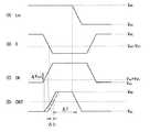
図6は、画素回路に印加される電圧波形の一例と、駆動トランジスタのゲート電圧およびソース電圧の変化の一例とを表したものである。図6(A)には信号線DTLに、信号電圧Vsigと、オフセット電圧Vofsが印加されている様子が示されている。図6(B)には書込線WSLに、駆動トランジスタをオンする電圧Vddと、駆動トランジスタをオフする電圧Vssが印加されている様子が示されている。図6(C)には電源線PSLに、ハイ電圧VccHと、ロー電圧VccLが印加されている様子が示されている。さらに、図6(D),(E)には、電源線PSL、信号線DTLおよび書込線WSLへの電圧印加に応じて、駆動トランジスタTr1のゲート電圧Vgおよびソース電圧Vsが時々刻々変化している様子が示されている。FIG. 6 shows an example of a voltage waveform applied to the pixel circuit and an example of changes in the gate voltage and source voltage of the driving transistor. FIG.6A shows a state in which the signal voltage Vsig and the offset voltage Vofs are applied to the signal line DTL. FIG. 6B shows a state where a voltage Vdd for turning on the driving transistor and a voltage Vss for turning off the driving transistor are applied to the writing line WSL. FIG.6C shows a state where the high voltage VccH and the low voltage VccL are applied to the power supply line PSL. Further, in FIGS. 6D and 6E, the gate voltage Vg and the source voltage Vs of the drive transistor Tr1 are sometimes changed depending on the voltage application to the power supply line PSL, the signal line DTL, and the write line WSL. It shows how it changes every moment.
図6から、1H内に2回、WSパルスP1が書込線WSLに印加されており、1回目のWSパルスP1によって閾値補正が行われ、2回目のWSパルスP1によって移動度補正と信号書き込みが行われていることがわかる。つまり、図6において、WSパルスP1は、信号書込みだけでなく、駆動トランジスタTr1の閾値補正や移動度補正にも用いられている。From FIG. 6, the WS pulse P1 is applied to the write line WSL twice within 1H, threshold correction is performed by the first WS pulse P1, and mobility correction and signal writing are performed by the second WS pulse P1. Can be seen. That is, in FIG. 6, WS pulse P1 is not only the signal writing is also used in the threshold correction and the mobility correction of the driving transistor Tr1.
以下、駆動トランジスタTr1の閾値補正および移動度補正について説明する。2回目のWSパルスP1の印加により、信号電圧Vsigが駆動トランジスタTr1のゲートに書き込まれる。これにより、駆動トランジスタTr1がオンし、駆動トランジスタTr1に電流が流れる。このとき、有機EL素子111に逆バイアスが印加されているとすると、駆動トランジスタTr1から流れ出た電荷は、保持容量Csおよび有機EL素子111の素子容量(図示せず)に充電され、ソース電圧Vsが上昇する。駆動トランジスタTr1の移動度が高い場合には、駆動トランジスタTr1に流れる電流が大きくなるので、ソース電圧Vsの上昇が早くなる。逆に、駆動トランジスタTr1の移動度が低い場合には、駆動トランジスタTr1に流れる電流が小さくなるので、駆動トランジスタTr1の移動度が高い場合と比べて、ソース電圧Vsの上昇が遅くなる。従って、移動度を補正する期間を調整することにより、移動度を補正することができる。Hereinafter, threshold correction and mobility correction of the drive transistor Tr1 will be described. By applying the WS pulse P1 for the second time, the signal voltage Vsig is written to the gate of the driving transistor Tr1 . As a result, the drive transistor Tr1 is turned on, and a current flows through the drive transistor Tr1 . At this time,assuming that a reverse bias is applied to the
ところで、アクティブマトリクス方式の表示装置では、信号線を駆動する水平駆動回路や、各画素を順次選択する書き込み走査回路は、いずれも基本的にシフトレジスタ(図示せず)を含んで構成されており、画素の各列または各行に対応して、1段ごとにバッファ回路を備えている。例えば、走査回路内のバッファ回路は、典型的には、図8に示したように、2つのインバータ回路210,220を直列に接続して構成されている。図8のバッファ回路200において、インバータ回路210は、pチャネル型のMOSトランジスタおよびnチャネル型のMOSトランジスタが並列接続された回路構成となっている。一方、インバータ回路220は、CMOSトランジスタおよびnチャネル型のMOSトランジスタが並列接続された回路構成となっている。バッファ回路200は、ハイレベルの電圧が印加される高電圧配線LHと、ローレベルの電圧が印加される低電圧配線LLとの間に挿入されている。By the way, in an active matrix display device, a horizontal drive circuit that drives signal lines and a write scanning circuit that sequentially selects each pixel basically include a shift register (not shown). A buffer circuit is provided for each stage corresponding to each column or each row of pixels. For example, the buffer circuit in the scanning circuit is typically configured by connecting two
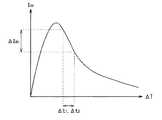
しかし、CMOSトランジスタにおいて、バッファ回路200では、例えば、図9に示したように、pチャネル型のMOSトランジスタの閾値電圧Vth1がΔVth1だけばらつくと、出力OUTの電圧Voutの立ち上がるタイミングがΔt1だけずれる。また、CMOSトランジスタにおいて、バッファ回路200では、例えば、図10に示したように、nチャネル型のMOSトランジスタの閾値電圧Vth2がΔVth2だけばらつくと、出力OUTの電圧Voutの立ち上るタイミングがΔt2だけずれる。従って、例えば、出力OUTの電圧Voutの立ち上がるタイミングがばらつき、移動度補正期間ΔTがΔt1またはΔt2だけばらついた場合には、例えば、図11に示したように、発光時の電流IdsがΔIdsだけばらつき、そのばらつきが輝度のばらつきとなってしまうという問題があった。なお、図11は、移動度補正期間ΔTと、発光輝度との関係の一例を表したものである。However, in the CMOS transistor, in the buffer circuit 200, for example, as shown in FIG. 9, when the threshold voltage Vth1 of the p-channel MOS transistor varies by ΔVth1 , the rising timing of the voltage Vout of the output OUT is Δt shifted by1. In the CMOS transistor, in the buffer circuit 200, for example, as shown in FIG. 10, when the threshold voltage Vth2 of the n-channel MOS transistor varies by ΔVth2, the timing at which the voltage Vout of the output OUT rises is Δt Deviation bytwo . Thus, for example, variations rising timing of the voltage Vout ofthe output OUT, when the mobility correction period ΔT is varied by Delta] t1 or Delta] t2, for example, as shown in FIG. 11, upon light emission current Ids However, there is a problem that the variation is ΔIds , and the variation is luminance variation. FIG. 11 shows an example of the relationship between the mobility correction period ΔT and the light emission luminance.
なお、閾値電圧Vthのばらつきの問題は、表示装置の走査回路に限って生じるものではなく、他のデバイスにおいても同様に生じ得るものである。Note that the problem of variation in the threshold voltage Vth does not occur only in the scanning circuit of the display device, but can occur in other devices as well.
本発明はかかる問題点に鑑みてなされたものであり、その目的は、出力電圧の立ち上がるタイミングのばらつきを低減することの可能な駆動回路、およびこの駆動回路を備えた表示装置を提供することにある。 The present invention has been made in view of such problems, and an object of the present invention is to provide a drive circuit capable of reducing variations in the rise timing of the output voltage, and a display device including the drive circuit. is there.
本発明の駆動回路は、互いに直列に接続されると共に高電圧線および低電圧線の間に挿入された入力側インバータ回路および出力側インバータ回路を備えている。出力側インバータ回路は、3つのトランジスタを有している。1つ目は、ドレインが高電圧線側に接続され、ソースが出力側インバータ回路の出力側に接続されたデュアルゲート型の第1導電型の第1トランジスタである。2つ目は、ドレインが高電圧線側に接続され、ソースが出力側インバータ回路の出力側に接続されたデュアルゲート型の第2導電型の第2トランジスタである。3つ目は、ドレインが低電圧線側に接続され、ソースが出力側インバータ回路の出力側に接続された第3トランジスタである。 The drive circuit of the present invention includes an input side inverter circuit and an output side inverter circuit that are connected in series with each other and inserted between a high voltage line and a low voltage line. The output side inverter circuit has three transistors. The first is a dual gate type first conductivity type first transistor having a drain connected to the high voltage line side and a source connected to the output side of the output side inverter circuit. The second is a dual gate type second conductivity type second transistor having a drain connected to the high voltage line side and a source connected to the output side of the output side inverter circuit. The third is a third transistor having a drain connected to the low voltage line side and a source connected to the output side of the output side inverter circuit.
本発明の表示装置は、行状に配置された複数の走査線と、列状に配置された複数の信号線と、行列状に配置された複数の画素とを含む表示部を備えており、さらに、各画素を駆動する駆動部を備えている。駆動部は、走査線ごとに1つずつ設けられた複数の駆動回路を有しており、駆動部内の各駆動回路は、上記の駆動回路と同一の構成要素を含んでいる。 The display device of the present invention includes a display unit including a plurality of scanning lines arranged in rows, a plurality of signal lines arranged in columns, and a plurality of pixels arranged in a matrix, And a driving unit for driving each pixel. The drive unit includes a plurality of drive circuits provided for each scanning line, and each drive circuit in the drive unit includes the same components as the above drive circuit.
本発明の駆動回路および表示装置では、互いに直列に接続された入力側インバータ回路および出力側インバータ回路のうち出力側インバータ回路に、デュアルゲート型のトランジスタが組み込まれている。これにより、一方のゲート電圧を制御し、トランジスタ特性を変動させることにより、トランジスタの閾値電圧をある一定の値に補正することができる。 In the drive circuit and the display device of the present invention, a dual-gate transistor is incorporated in the output-side inverter circuit among the input-side inverter circuit and the output-side inverter circuit connected in series. Thus, the threshold voltage of the transistor can be corrected to a certain value by controlling one of the gate voltages and changing the transistor characteristics.
本発明の駆動回路および表示装置によれば、デュアルゲート型のトランジスタのゲート電圧を制御して、トランジスタの閾値電圧をある一定の値に補正することができるようにした。これにより、駆動回路の出力電圧が立ち上がるタイミングにおいて、ばらつきを低減することができる。従って、例えば、有機EL表示装置においては、発光時に有機EL素子に流れる電流のばらつきを低減することができるので、輝度の均一性を向上させることができる。 According to the driving circuit and the display device of the present invention, the gate voltage of the dual gate type transistor is controlled so that the threshold voltage of the transistor can be corrected to a certain value. Thereby, the variation can be reduced at the timing when the output voltage of the drive circuit rises. Therefore, for example, in an organic EL display device, variation in current flowing through the organic EL element during light emission can be reduced, so that uniformity of luminance can be improved.
以下、発明を実施するための形態について、図面を参照して詳細に説明する。なお、説明は以下の順序で行う。
1.実施の形態(図1〜図3)
2.適用例(図4〜図6)
3.従来技術の説明(図7〜図11)
DESCRIPTION OF EMBODIMENTS Hereinafter, embodiments for carrying out the invention will be described in detail with reference to the drawings. The description will be given in the following order.
1. Embodiment (FIGS. 1 to 3)
2. Application examples (Figs. 4-6)
3. Description of prior art (FIGS. 7 to 11)
<実施の形態>
[構成]
図1は、本発明の一実施の形態に係るバッファ回路1(駆動回路)の全体構成の一例を表したものである。バッファ回路1は、入力端INに入力されたパルス信号の位相とほぼ同一位相のパルス信号を出力端OUTから出力するものである。バッファ回路1は、インバータ回路10(入力側インバータ回路)およびインバータ回路20(出力側インバータ回路)を備えている。<Embodiment>
[Constitution]
FIG. 1 shows an example of the overall configuration of a buffer circuit 1 (drive circuit) according to an embodiment of the present invention. The
インバータ回路10,20は、入力されたパルス信号の信号波形をほぼ反転させたパルス信号を出力するものである。インバータ回路10,20は、互いに直列に接続されている。インバータ回路10は、インバータ回路20との関係で入力端IN側に配置されており、インバータ回路10の入力端がバッファ回路1の入力端INに相当している。一方、インバータ回路20は、インバータ回路10との関係で出力端OUT側に配置されており、インバータ回路20の出力端がバッファ回路1の出力端OUTに相当している。インバータ回路10の出力端(図中のAに対応する箇所)は、インバータ回路20の入力端に接続されており、バッファ回路1は、インバータ回路10の出力がインバータ回路20に入力されるように構成されている。 The
インバータ回路10は、高電圧線LH1および低電圧線LLの間に挿入されており、インバータ回路20は、高電圧線LH2および低電圧線LLの間に挿入されている。ここで、高電圧線LH1および高電圧線LH2は、互いに分離独立しており、高電圧線LH1および高電圧線LH2に対して互いに異なる電圧を印加することが可能となっている。The
インバータ回路10は、第1導電型のトランジスタTr11と、第2導電型のトランジスタTr12とを有している。トランジスタTr11は、例えば、pチャネル型のMOS(金属酸化膜半導体: Metal Oxide Semiconductor)トランジスタであり、トランジスタTr12は、例えば、nチャネル型のMOSトランジスタである。The
トランジスタTr11およびトランジスタTr12は、互いに並列接続されている。具体的には、トランジスタTr11およびトランジスタTr12のそれぞれのゲートが互いに接続されている。さらに、トランジスタTr11のソースまたはドレインと、トランジスタTr12のソースまたはドレインとが互いに接続されている。また、トランジスタTr11およびトランジスタTr12のそれぞれのゲートは、インバータ回路10の入力端(バッファ回路1の入力端IN)に接続されている。トランジスタTr11のソースまたはドレインと、トランジスタTr12のソースまたはドレインとの接続点Aは、インバータ回路10の出力端に接続されている。トランジスタTr11のソースおよびドレインのうちトランジスタTr12に未接続の方は高電圧線LHに接続されている。一方、トランジスタTr12のソースおよびドレインのうちトランジスタTr11に未接続の方は低電圧線LLに接続されている。なお、インバータ回路10において、何らかの素子が、トランジスタTr11とトランジスタTr12との間や、トランジスタTr11と高電圧線LHとの間、トランジスタTr12と低電圧線LLとの間に設けられていてもよい。Transistor Tr11 and the transistor Tr12 is connected in parallel to each other. Specifically, the gates of the transistors Tr11 and Tr12 are connected to each other. Further, the source or drain of the transistor Tr11 and the source or drain of the transistor Tr12 are connected to each other. The gates of the transistors Tr11 and Tr12 are connected to the input terminal of the inverter circuit 10 (the input terminal IN of the buffer circuit 1). A connection point A between the source or drain of the transistor Tr11 and the source or drain of the transistor Tr12 is connected to the output terminal of the
インバータ回路20は、第1導電型のトランジスタTr21(第1トランジスタ)と、第2導電型のトランジスタTr22(第2トランジスタ)と、第1導電型のトランジスタTr23(第3トランジスタ)とを有している。トランジスタTr21は、例えば、pチャネル型のMOSトランジスタであり、トランジスタTr22,Tr23は、例えば、nチャネル型のMOSトランジスタである。The
トランジスタTr21,Tr22は、デュアルゲート型のトランジスタであり、それぞれ、2つのゲート電極を有している。ここで、2つのゲート電極のうち一方の電極は、バッファ回路1の入力端INに入力された信号が入力される電極であり、図1におけるゲート電極g1,g3に相当する。また、2つのゲート電極のうち他方の電極は、トランジスタの特性を変化させる制御信号が入力される電極であり、図1におけるゲート電極g2,g4に相当する。ゲート電極g2,g4は、バックゲート電極とも呼ばれるものである。例えば、図2に示したように、ゲート電極g2,g4に小さな電圧Vbを入力した場合には、トランジスタTr21,Tr22の閾値電圧Vthを大きくすることができる。逆に、例えば、図2に示したように、ゲート電極g2,g4に大きな電圧Vbを入力した場合には、トランジスタTr21,Tr22の閾値電圧Vthを小さくすることができる。このように、ゲート電極g2,g4に印加する電圧の大きさを制御することにより、トランジスタTr21,Tr22の動作点を移動させることができる。従って、トランジスタTr21,Tr22に入力する制御信号の振幅を調整することにより、トランジスタTr21,Tr22の閾値電圧を調整することができる。The transistors Tr21 and Tr22 are dual gate type transistors, each having two gate electrodes. Here, one of the two gate electrodes is an electrode to which a signal input to the input terminal IN of the
トランジスタTr21およびトランジスタTr23は、互いに並列接続されている。具体的には、トランジスタTr21およびトランジスタTr23のそれぞれのゲートが互いに接続されている。さらに、トランジスタTr21のソースまたはドレインと、トランジスタTr23のソースまたはドレインとが互いに接続されている。また、トランジスタTr21およびトランジスタTr23のそれぞれのゲートは、インバータ回路10の出力端に接続されている。トランジスタTr21のソースまたはドレインと、トランジスタTr23のソースまたはドレインとの接続点Bは、インバータ回路20の出力端に接続されている。トランジスタTr21のソースおよびドレインのうちトランジスタTr23に未接続の方は高電圧線LH2に接続されている。トランジスタTr22のソースまたはドレインと、トランジスタTr23のソースまたはドレインとの接続点Cは、トランジスタTr23のソースおよびドレインのうち低電圧線LLに未接続な方と、インバータ回路20の出力端とに接続されている。トランジスタTr22のソースおよびドレインのうちトランジスタTr23に未接続の方は高電圧線LH2に接続されている。トランジスタTr23のソースおよびドレインのうちトランジスタTr21に未接続の方は低電圧線LLに接続されている。トランジスタTr21のバックゲートは、制御線Lb1に接続されている。また、トランジスタTr22のバックゲートは、制御線Lb2に接続されている。なお、インバータ回路10において、何らかの素子が、トランジスタTr21とトランジスタTr23との間や、トランジスタTr21と高電圧線LHとの間、トランジスタTr23と低電圧線LLとの間に設けられていてもよい。The transistor Tr21 and the transistor Tr23 are connected in parallel to each other. Specifically, the gates of the transistors Tr21 and Tr23 are connected to each other. Further, the source or drain of the transistor Tr21 and the source or drain of the transistor Tr23 are connected to each other. The gates of the transistors Tr21 and Tr23 are connected to the output terminal of the
[動作]
次に、本実施の形態のバッファ回路1の動作について説明する。以下では、主として、バッファ回路1における閾値補正(Vthキャンセル)について説明する。[Operation]
Next, the operation of the
図3は、バッファ回路1の動作の一例を表したものである。図3には、トランジスタTr21のゲート−ソース間電圧Vgsに含まれる閾値電圧Vthをキャンセルする動作の一例が示されている。FIG. 3 shows an example of the operation of the
当初、バッファ回路1の入力端INにはVssが入力されており、接続点A(インバータ回路10の出力端)の電圧がVddとなっている。そのため、トランジスタTr21,Tr22がオフしており、トランジスタTr23がオンしているので、バッファ回路1の出力端OUTの電圧がVssとなっている。次に、入力端INの電圧がVssからVddに立ち上る(T1)。すると、接続点Aの電圧がVddからVssに立ち下がる。そのため、トランジスタTr21,Tr22がオンし、トランジスタTr23がオフするので、出力端OUTの電圧がVssからVddに変化する。次に、高電圧線LH2の電圧が、VddからVssに変化する(T2)。すると、出力端OUTの電圧もVddからVssに変化する。次に、入力端INの電圧がVddからVssに立ち下がる(T3)。すると、接続点Aの電圧がVssからVddに立ち上るが、高電圧線LH2の電圧がすでにVssになっているので、トランジスタTr21,Tr22はオフしたままであり、出力端OUTの電圧はVssを維持する。Initially, Vss is input to the input terminal IN of the
ところで、出力端OUTの電圧の立ち上がり波形は、入力端INの電圧が印加されるトランジスタTr21の特性と、接続点Aの電圧が入力されるトランジスタTr22の特性に依っている。従って、トランジスタTr21,Tr22の閾値電圧Vthにばらつきがある場合には、出力電圧がVssからVddに立ち上がるタイミングにおいて、ばらつきが発生して、出力電圧のパルス幅が所望の値からずれてしまう。そのため、バッファ回路1を、例えば、有機EL表示装置のスキャナの出力段に適用し、移動度補正期間をバッファ回路1の出力電圧のパルス幅で規定した場合には、移動度補正期間がばらついてしまい、発光時に有機EL素子に流れる電流もばらついてしまう。その結果、輝度が不均一となってしまうという問題がある。Incidentally, the rising waveform of the voltage at the output terminal OUT depends on the characteristics of the transistor Tr21 to which the voltage at the input terminal IN is applied and the characteristics of the transistor Tr22 to which the voltage at the connection point A is input. Therefore, when the threshold voltages Vth of the transistors Tr21 and Tr22 are varied, variations occur at the timing when the output voltage rises from Vss to Vdd, and the pulse width of the output voltage is changed from a desired value. It will shift. Therefore, for example, when the
一方、本実施の形態では、ゲート電極g2,g4に制御信号を印加して、トランジスタTr21,Tr22の閾値電圧を所望の値に調整することができる。これにより、バッファ回路1の出力電圧が立ち上がるタイミングにおいて、ばらつきを低減することができる。従って、バッファ回路1を、例えば、有機EL表示装置のスキャナの出力段に適用し、移動度補正期間をバッファ回路1の出力電圧のパルス幅で規定した場合であっても、移動度補正期間のばらつきが少なく、発光時に有機EL素子に流れる電流のばらつきを低減することができる。その結果、輝度の均一性を向上させることができる。On the other hand, in this embodiment, the threshold voltage of the transistors Tr21 and Tr22 can be adjusted to a desired value by applying a control signal to the gate electrodes g2 and g4. Thereby, the variation can be reduced at the timing when the output voltage of the
<適用例>
図4は、上記実施の形態に係るバッファ回路1の適用例の一例である表示装置100の全体構成の一例を表したものである。この表示装置100は、例えば、表示パネル110(表示部)と、駆動回路120(駆動部)とを備えている。<Application example>
FIG. 4 illustrates an example of the entire configuration of the display device 100 as an example of application of the
(表示パネル110)
表示パネル110は、発光色の互いに異なる3種類の有機EL素子111R,111G,111Bが2次元配置された表示領域110Aを有している。表示領域110Aとは、有機EL素子111R,111G,111Bから発せられる光を利用して映像を表示する領域である。有機EL素子111Rは赤色光を発する有機EL素子であり、有機EL素子111Gは緑色光を発する有機EL素子であり、有機EL素子111Bは青色光を発する有機EL素子である。なお、以下では、有機EL素子111R,111G,111Bの総称として有機EL素子111を適宜、用いるものとする。(Display panel 110)
The
(表示領域110A)
図5は、表示領域10A内の回路構成の一例を、後述の書込線駆動回路124の一例と共に表したものである。表示領域110A内には、複数の画素回路112が個々の有機EL素子111と対となって2次元配置されている。なお、本適用例では、一対の有機EL素子111および画素回路112が1つの画素113を構成している。より詳細には、図5に示したように、一対の有機EL素子111Rおよび画素回路112が1つの赤色用の画素113Rを構成し、一対の有機EL素子111Gおよび画素回路112が1つの緑色用の画素113Gを構成し、一対の有機EL素子111Bおよび画素回路112が1つの青色用の画素113Bを構成している。さらに、互いに隣り合う3つの画素113R,113G,113Bが1つの表示画素114を構成している。(
FIG. 5 illustrates an example of a circuit configuration in the
各画素回路112は、例えば、有機EL素子111に流れる電流を制御する駆動トランジスタTr1と、信号線DTLの電圧を駆動トランジスタTr1に書き込む書き込みトランジスタTr2と、保持容量Csとによって構成されたものであり、2Tr1Cの回路構成となっている。駆動トランジスタTr1および書き込みトランジスタTr2は、例えば、nチャネルMOS型の薄膜トランジスタ(TFT(Thin Film Transistor))により形成されている。駆動トランジスタTr1または書き込みトランジスタTr2は、例えば、pチャネルMOS型のTFTであってもよい。Each
表示領域110Aにおいて、複数の書込線WSL(走査線)が行状に配置され、複数の信号線DTLが列状に配置されている。表示領域110Aには、さらに、複数の電源線PSL(電源電圧の供給される部材)が書込線WSLに沿って行状に配置されている。各信号線DTLと各書込線WSLとの交差点近傍には、有機EL素子111が1つずつ設けられている。各信号線DTLは、後述の信号線駆動回路123の出力端(図示せず)と、書き込みトランジスタTr2のドレイン電極およびソース電極のいずれか一方(図示せず)に接続されている。各書込線WSLは、後述の書込線駆動回路124の出力端(図示せず)と、書き込みトランジスタTr2のゲート電極(図示せず)に接続されている。各電源線PSLは、後述の電源線駆動回路125の出力端(図示せず)と、駆動トランジスタTr1のドレイン電極およびソース電極のいずれか一方(図示せず)に接続されている。書き込みトランジスタTr2のドレイン電極およびソース電極のうち信号線DTLに非接続の方(図示せず)は、駆動トランジスタTr1のゲート電極(図示せず)と、保持容量Csの一端に接続されている。駆動トランジスタTr1のドレイン電極およびソース電極のうち電源線PSLに非接続の方(図示せず)と保持容量Csの他端とが、有機EL素子111のアノード電極(図示せず)に接続されている。有機EL素子111のカソード電極(図示せず)は、例えば、グラウンド線GNDに接続されている。In the
(駆動回路120)
次に、駆動回路120内の各回路について、図4、図5を参照して説明する。駆動回路120は、タイミング生成回路121、映像信号処理回路122、信号線駆動回路123、書込線駆動回路124、および電源線駆動回路125を有している。(Drive circuit 120)
Next, each circuit in the
タイミング生成回路121は、映像信号処理回路122、信号線駆動回路123、書込線駆動回路124、および電源線駆動回路125が連動して動作するように制御するものである。タイミング生成回路121は、例えば、外部から入力された同期信号20Bに応じて(同期して)、上述した各回路に対して制御信号121Aを出力するようになっている。 The
映像信号処理回路122は、外部から入力された映像信号120Aに対して所定の補正を行うと共に、補正した後の映像信号122Aを信号線駆動回路123に出力するようになっている。所定の補正としては、例えば、ガンマ補正や、オーバードライブ補正などが挙げられる。 The video
信号線駆動回路123は、制御信号121Aの入力に応じて(同期して)、映像信号処理回路122から入力された映像信号122A(信号電圧Vsig)を各信号線DTLに印加して、選択対象の画素113に書き込むものである。なお、書き込みとは、駆動トランジスタTr1のゲートに所定の電圧を印加することを指している。In response to (in synchronization with) the input of the
信号線駆動回路123は、例えばシフトレジスタ(図示せず)を含んで構成されており、画素113の各列に対応して、1段ごとにバッファ回路(図示せず)を備えている。この信号線駆動回路123は、制御信号121Aの入力に応じて(同期して)、各信号線DTLに対して、2種類の電圧(Vofs、Vsig)を出力可能となっている。具体的には、信号線駆動回路123は、各画素113に接続された信号線DTLを介して、書込線駆動回路124により選択された画素113へ2種類の電圧(Vofs、Vsig)を順番に供給するようになっている。The signal
ここで、オフセット電圧Vofsは、有機EL素子111の閾値電圧Velよりも低い電圧値となっている。また、信号電圧Vsigは、映像信号122Aに対応する電圧値となっている。信号電圧Vsigの最小電圧はオフセット電圧Vofsよりも低い電圧値となっており、信号電圧Vsigの最大電圧はオフセット電圧Vofsよりも高い電圧値となっている。Here, the offset voltage Vofs has a voltage value lower than the threshold voltage Vel of the
書込線駆動回路124は、例えばシフトレジスタ(図示せず)を含んで構成されており、画素113の各行に対応して、1段ごとにバッファ回路1を備えている。この書込線駆動回路124は、制御信号121Aの入力に応じて(同期して)、各書込線WSLに対して、2種類の電圧(Vdd、Vss)を出力可能となっている。具体的には、書込線駆動回路124は、各画素113に接続された書込線WSLを介して、駆動対象の画素113へ2種類の電圧(Vdd、Vss)を供給し、書き込みトランジスタTr2を制御するようになっている。The write
ここで、電圧Vddは、書き込みトランジスタTr2のオン電圧以上の値となっている。Vddは、後述の消光時や閾値補正時に、書込線駆動回路124から出力される電圧値である。Vssは、書き込みトランジスタTr2のオン電圧よりも低い値となっており、かつ、Vddよりも低い値となっている。Here, the voltage Vdd is a value equal to or higher than the ON voltage of the write transistor Tr2 . Vdd is a voltage value output from the write
電源線駆動回路125は、例えばシフトレジスタ(図示せず)を含んで構成されており、例えば、画素113の各行に対応して、1段ごとにバッファ回路(図示せず)を備えている。この電源線駆動回路125は、制御信号121Aの入力に応じて(同期して)、2種類の電圧(VccH、VccL)を出力可能となっている。具体的には、電源線駆動回路125は、各画素113に接続された電源線PSLを介して、駆動対象の画素113へ2種類の電圧(VccH、VccL)を供給し、有機EL素子111の発光および消光を制御するようになっている。The power supply
ここで、電圧VccLは、有機EL素子111の閾値電圧Velと、有機EL素子111のカソードの電圧Vcaとを足し合わせた電圧(Vel+Vca)よりも低い電圧値である。また、電圧VccHは、電圧(Vel+Vca)以上の電圧値である。Here, the voltage VccL is a voltage value lower than a voltage (Vel + Vca ) obtained by adding the threshold voltage Vel of the
次に、本適用例の表示装置100の動作(消光から発光までの動作)の一例について説明する。本適用例では、駆動トランジスタTr1の閾値電圧Vthや移動度μが経時変化したりしても、それらの影響を受けることなく、有機EL素子111の発光輝度を一定に保つようにするために、閾値電圧Vthや移動度μの変動に対する補正動作が組み込まれている。Next, an example of the operation (operation from extinction to light emission) of the display device 100 of this application example will be described. In this application example, even if the threshold voltage Vth and the mobility μ of the driving transistor Tr1 change with time, the light emission luminance of the
図6は、画素回路112に印加される電圧波形の一例と、駆動トランジスタTr1のゲート電圧Vgおよびソース電圧Vsの変化の一例とを表したものである。図6(A)には信号線DTLに、信号電圧Vsigと、オフセット電圧Vofsが印加されている様子が示されている。図6(B)には書込線WSLに、駆動トランジスタTr1をオンする電圧Vddと、駆動トランジスタTr1をオフする電圧Vssが印加されている様子が示されている。図6(C)には電源線PSLに、電圧VccHと、電圧VccLが印加されている様子が示されている。さらに、図6(D),(E)には、電源線PSL、信号線DTLおよび書込線WSLへの電圧印加に応じて、駆動トランジスタTr1のゲート電圧Vgおよびソース電圧Vsが時々刻々変化している様子が示されている。FIG. 6 illustrates an example of a voltage waveform applied to the
(Vth補正準備期間)
まず、Vth補正の準備を行う。具体的には、書込線WSLの電圧がVoffとなっており、信号線DTLの電圧がVsigとなっており、電源線DSLの電圧がVccHとなっている時(つまり有機EL素子111が発光している時)に、電源線駆動回路125が電源線DSLの電圧をVccHからVccLに下げる(T1)。すると、ソース電圧VsがVccLとなり、有機EL素子111が消光する。次に、信号線駆動回路123が信号線DTLの電圧をVsigからVofsに切り替えたのち、電源線DSLの電圧がVccHとなっている間に、書込線駆動回路124が書込線WSLの電圧をVoffからVonに上げる。すると、ゲート電圧VgがVofsに下がる。このとき、ゲート−ソース間電圧Vgs(=Vofs−VccL)が駆動トランジスタTr1の閾値電圧Vthよりも大きくなるように、電源線駆動回路125および信号線駆動回路123では、電源線DSLおよび信号線DTLへの印加電圧(VccL、Vofs)が設定されている。(Vth correction preparation period)
First, preparation for Vth correction is performed. Specifically, when the voltage of the write line WSL is Voff , the voltage of the signal line DTL is Vsig, and the voltage of the power supply line DSL is VccH (that is, the organic EL element) when) where 111 is emitting light, the power supply
(最初のVth補正期間)
次に、Vthの補正を行う。具体的には、信号線DTLの電圧がVofsとなっている間に、電源線駆動回路125が電源線DSLの電圧をVccLからVccHに上げる(T2)。すると、駆動トランジスタTr1のドレイン−ソース間に電流Idsが流れ、ソース電圧Vsが上昇する。その後、信号線駆動回路123が信号線DTLの電圧をVofsからVsigに切り替える前に、書込線駆動回路124が書込線WSLの電圧をVonからVoffに下げる(T3)。すると、駆動トランジスタTr1のゲートがフローティングとなり、Vthの補正が停止する。(First Vth correction period)
Next, Vth is corrected. Specifically, while the voltage of the signal line DTL is Vofs, the power supply
(最初のVth補正休止期間)
Vth補正が休止している期間中は、例えば、先のVth補正を行った行(画素)とは異なる他の行(画素)において、信号線DTLの電圧のサンプリングが行われる。なお、このとき、先のVth補正を行った行(画素)において、ソース電圧VsがVofs−Vthよりも低いので、Vth補正休止期間中にも、先のVth補正を行った行(画素)において、駆動トランジスタTr1のドレイン−ソース間に電流Idsが流れ、ソース電圧Vsが上昇し、保持容量Csを介したカップリングによりゲート電圧Vgも上昇する。(First Vth correction pause period)
During the period in which the Vth correction is paused, for example, the voltage of the signal line DTL is sampled in another row (pixel) that is different from the row (pixel) that has been subjected to the previous Vth correction. At this time, in the line from which the previous Vth correction (pixels), since the source voltage Vs is lower than Vofs -Vth, even during the Vth correction stop period, subjected to previous Vth correction In the same row (pixel), the current Ids flows between the drain and source of the drive transistor Tr1 , the source voltage Vs rises, and the gate voltage Vg also rises due to coupling through the storage capacitor Cs .
(2回目のVth補正期間)
次に、Vth補正を再び行う。具体的には、信号線DTLの電圧がVofsとなっており、Vth補正が可能となっている時に、書込線駆動回路124が書込線WSLの電圧をVoffからVonに上げ、駆動トランジスタTr1のゲートをVofsにする(T4)。このとき、ソース電圧VsがVofs−Vthよりも低い場合(Vth補正がまだ完了していない場合)には、駆動トランジスタTr1がカットオフするまで(ゲート−ソース間電圧VgsがVthになるまで)、駆動トランジスタTr1のドレイン−ソース間に電流Idsが流れる。その後、信号線駆動回路123が信号線DTLの電圧をVofsからVsigに切り替える前に、書込線駆動回路124が書込線WSLの電圧をVonからVoffに下げる(T5)。すると、駆動トランジスタTr1のゲートがフローティングとなるので、ゲート−ソース間電圧Vgsを信号線DTLの電圧の大きさに拘わらず一定に維持することができる。(Second Vth correction period)
Next, Vth correction is performed again. Specifically, when the voltage of the signal line DTL is Vofs and Vth correction is possible, the write
なお、このVth補正期間において、保持容量CsがVthに充電され、ゲート−ソース間電圧VgsがVthとなった場合には、駆動回路120は、Vth補正を終了する。しかし、ゲート−ソース間電圧VgsがVthにまで到達しない場合には、駆動回路120は、ゲート−ソース間電圧VgsがVthに到達するまで、Vth補正と、Vth補正休止とを繰り返し実行する。In this Vth correction period, when the storage capacitor Cs is charged to Vth and the gate-source voltage Vgs becomes Vth , the
(書き込み・μ補正期間)
Vth補正休止期間が終了した後、書き込みとμ補正を行う。具体的には、信号線DTLの電圧がVsigとなっている間に、書込線駆動回路124が書込線WSLの電圧をVoffからVonに上げ(T6)、駆動トランジスタTr1のゲートを信号線DTLに接続する。すると、駆動トランジスタTr1のゲート電圧Vgが信号線DTLの電圧Vsigとなる。このとき、有機EL素子111のアノード電圧はこの段階ではまだ有機EL素子111の閾値電圧Velよりも小さく、有機EL素子111はカットオフしている。そのため、電流Idsは有機EL素子111の素子容量(図示せず)に流れ、素子容量が充電されるので、ソース電圧VsがΔVxだけ上昇し、やがてゲート−ソース間電圧VgsがVsig+Vth−ΔVxとなる。このようにして、書き込みと同時にμ補正が行われる。ここで、駆動トランジスタTr1の移動度μが大きい程、ΔVxも大きくなるので、ゲート−ソース間電圧Vgsを発光前にΔVxだけ小さくすることにより、画素113ごとの移動度μのばらつきを取り除くことができる。(Writing / μ correction period)
After the end of the Vth correction pause period, writing and μ correction are performed. Specifically, while the voltage of the signal line DTL is Vsig, the write
(発光期間)
最後に、書込線駆動回路124が書込線WSLの電圧をVonからVoffに下げる(T8)。すると、駆動トランジスタTr1のゲートがフローティングとなり、駆動トランジスタTr1のドレイン−ソース間に電流Idsが流れ、ソース電圧Vsが上昇する。その結果、有機EL素子111に閾値電圧Vel以上の電圧が印加され、有機EL素子111が所望の輝度で発光する。(Light emission period)
Finally, the write
本適用例の表示装置100では、上記のようにして、各画素113において画素回路112がオンオフ制御され、各画素113の有機EL素子111に駆動電流が注入されることにより、正孔と電子とが再結合して発光が起こり、その光が外部に取り出される。その結果、表示パネル110の表示領域110Aにおいて画像が表示される。 In the display device 100 of this application example, as described above, the
ところで、従来では、アクティブマトリクス方式の表示装置において、走査回路内のバッファ回路は、典型的には、図8に示したように、2つのインバータ回路210,220を直列に接続して構成されている。しかし、バッファ回路200では、例えば、図9に示したように、pチャネル型のMOSトランジスタの閾値電圧Vth1がΔVth1だけばらつくと、出力OUTの電圧Voutの立ち上がるタイミングがΔt1だけずれる。また、バッファ回路200では、例えば、図10に示したように、nチャネル型のMOSトランジスタの閾値電圧Vth2がΔVth2だけばらつくと、出力OUTの電圧Voutの立ち下がるタイミングがΔt2だけずれる。従って、例えば、出力OUTの電圧Voutの立ち上がるタイミングおよび立ち下がるタイミングがばらつき、移動度補正期間ΔTがΔt1+Δt2だけばらついた場合には、例えば、図11に示したように、発光時の電流IdsがΔIdsだけばらつき、そのばらつきが輝度のばらつきとなってしまう。Incidentally, conventionally, in an active matrix display device, a buffer circuit in a scanning circuit is typically configured by connecting two
一方、本適用例では、上記実施の形態に係るバッファ回路1が書込線駆動回路124の出力段に用いられている。これにより、移動度補正期間をバッファ回路1の出力電圧のパルス幅で規定することができる。これにより、移動度補正期間のばらつきを低減することができるので、発光時に有機EL素子111に流れる電流Idsのばらつきを低減することができ、輝度の均一性を向上させることができる。On the other hand, in this application example, the
以上、実施の形態および適用例を挙げて本発明を説明したが、本発明は上記実施の形態等に限定されるものではなく、種々変形が可能である。 The present invention has been described above with the embodiments and application examples. However, the present invention is not limited to the above-described embodiments and the like, and various modifications can be made.
例えば、上記適用例では、上記実施の形態に係るバッファ回路1が書込線駆動回路124の出力段に用いられていたが、書込線駆動回路124の出力段の代わりに、電源線駆動回路125の出力段に用いられていてもよいし、書込線駆動回路124の出力段と共に、電源線駆動回路125の出力段に用いられていてもよい。 For example, in the application example, the
また、上記実施の形態等において、Vth補正動作前のトランジスタTr22のゲート電圧はVdd+Vth1よりも低くなっていればよく、Vth補正動作前のトランジスタTr21のゲート電圧はVss+Vth2よりも高くなっていればよい。従って、Vth補正動作前のトランジスタTr22のゲート電圧を設定する際に、高電圧線LH1,LH2以外の電圧線を使用してもよい。また、Vth補正動作前のトランジスタTr21のゲート電圧を設定する際に、低電圧線LL1,LL2以外の電圧線を使用してもよい。In the above-described embodiment and the like, the gate voltage of the transistor Tr22 before the Vth correction operation may be lower than Vdd + Vth1 , and the gate voltage of the transistor Tr21 before the Vth correction operation is Vss. What is necessary is just to become higher than +Vth2 . Therefore, when setting the gate voltage of the transistor Tr22 before the Vth correction operation, a voltage line other than the high voltage lines LH1 and LH2 may be used. Further, when setting the gate voltage of the transistor Tr21 before the Vth correction operation, a voltage line other than the low voltage lines LL1 and LL2 may be used.
1,200…バッファ回路、10,20,210,220…インバータ回路、100…表示装置、110…表示パネル、110A…表示領域、111,111R,111G,111B…有機EL素子、112…画素回路、113,113R,113G,113B…画素、114…表示画素、120…駆動回路、120A,122A…映像信号、120B…同期信号、121…タイミング生成回路、121A…制御信号、122…映像信号処理回路、123…信号線駆動回路、124…書込線駆動回路、125…電源線駆動回路、A,B…接続点、Cs…保持容量、DTL…信号線、g1,g2,g3,g4…ゲート電極、GND…グラウンド線、IN…入力端、Ids…電流、LH1,LH2…高電圧線、LL1,LL2…低電圧線、OUT…出力端、PSL…電源線、Tr1…駆動トランジスタ、Tr2…書き込みトランジスタ、Tr11,Tr12,Tr21,Tr22,Tr23…トランジスタ、VCCH,VCCL,Vdd,Vss,ΔVx…電圧、Vd…ドレイン電圧、Vg…ゲート電圧、Vgs…ゲート−ソース間電圧、Vofs…オフセット電圧、Vs…ソース電圧、Vsig…信号電圧、Vth,Vth1,Vth2,Vel…閾値電圧、WSL…書込線、μ…移動度、ΔT…移動度補正期間。DESCRIPTION OF SYMBOLS 1,200 ...
Claims (2)
Translated fromJapanese前記出力側インバータ回路は、
ドレインが前記高電圧線側に接続され、ソースが当該出力側インバータ回路の出力側に接続されたデュアルゲート型の第1導電型の第1トランジスタと、
ドレインが前記高電圧線側に接続され、ソースが当該出力側インバータ回路の出力側に接続されたデュアルゲート型の第2導電型の第2トランジスタと、
ドレインが前記低電圧線側に接続され、ソースが当該出力側インバータ回路の出力側に接続された第3トランジスタと
を有する
駆動回路。An input-side inverter circuit and an output-side inverter circuit connected in series with each other and inserted between a high-voltage line and a low-voltage line;
The output-side inverter circuit is
A dual-gate first-conductivity-type first transistor having a drain connected to the high-voltage line side and a source connected to the output side of the output-side inverter circuit;
A dual gate type second conductivity type second transistor having a drain connected to the high voltage line side and a source connected to the output side of the output side inverter circuit;
And a third transistor having a drain connected to the low-voltage line side and a source connected to the output side of the output-side inverter circuit.
各画素を駆動する駆動部と
を備え、
前記駆動部は、前記走査線ごとに1つずつ設けられた複数の駆動回路を有し、
前記駆動回路は、互いに直列に接続されると共に高電圧線および低電圧線の間に挿入された入力側インバータ回路および出力側インバータ回路を有し、
前記出力側インバータ回路は、
ドレインが前記高電圧線側に接続され、ソースが当該出力側インバータ回路の出力側に接続されたデュアルゲート型の第1導電型の第1トランジスタと、
ドレインが前記高電圧線側に接続され、ソースが当該出力側インバータ回路の出力側に接続されたデュアルゲート型の第2導電型の第2トランジスタと、
ドレインが前記低電圧線側に接続され、ソースが当該出力側インバータ回路の出力側に接続された第3トランジスタと、
前記第1トランジスタおよび前記第2トランジスタのゲート電圧の補正を行う補正回路と
を有する
表示装置。A display unit including a plurality of scanning lines arranged in rows, a plurality of signal lines arranged in columns, and a plurality of pixels arranged in a matrix;
And a driving unit for driving each pixel,
The drive unit includes a plurality of drive circuits provided one for each scanning line,
The drive circuit includes an input side inverter circuit and an output side inverter circuit that are connected in series with each other and inserted between the high voltage line and the low voltage line,
The output-side inverter circuit is
A dual-gate first-conductivity-type first transistor having a drain connected to the high-voltage line side and a source connected to the output side of the output-side inverter circuit;
A dual gate type second conductivity type second transistor having a drain connected to the high voltage line side and a source connected to the output side of the output side inverter circuit;
A third transistor having a drain connected to the low-voltage line side and a source connected to the output side of the output-side inverter circuit;
And a correction circuit configured to correct gate voltages of the first transistor and the second transistor.
Priority Applications (3)
| Application Number | Priority Date | Filing Date | Title |
|---|---|---|---|
| JP2009295551AJP2011135523A (en) | 2009-12-25 | 2009-12-25 | Drive circuit and display device |
| US12/972,731US20110157118A1 (en) | 2009-12-25 | 2010-12-20 | Drive circuit and display device |
| CN2010106206207ACN102110415A (en) | 2009-12-25 | 2010-12-20 | Drive circuit and display device |
Applications Claiming Priority (1)
| Application Number | Priority Date | Filing Date | Title |
|---|---|---|---|
| JP2009295551AJP2011135523A (en) | 2009-12-25 | 2009-12-25 | Drive circuit and display device |
Publications (1)
| Publication Number | Publication Date |
|---|---|
| JP2011135523Atrue JP2011135523A (en) | 2011-07-07 |
Family
ID=44174552
Family Applications (1)
| Application Number | Title | Priority Date | Filing Date |
|---|---|---|---|
| JP2009295551AAbandonedJP2011135523A (en) | 2009-12-25 | 2009-12-25 | Drive circuit and display device |
Country Status (3)
| Country | Link |
|---|---|
| US (1) | US20110157118A1 (en) |
| JP (1) | JP2011135523A (en) |
| CN (1) | CN102110415A (en) |
Cited By (5)
| Publication number | Priority date | Publication date | Assignee | Title |
|---|---|---|---|---|
| JP2013055651A (en)* | 2011-08-05 | 2013-03-21 | Semiconductor Energy Lab Co Ltd | Pulse signal output circuit and shift register |
| CN103117042A (en)* | 2013-02-22 | 2013-05-22 | 合肥京东方光电科技有限公司 | Pixel unit drive circuit, pixel unit drive method, pixel unit and display device |
| JP2013157731A (en)* | 2012-01-27 | 2013-08-15 | Toshiba Corp | Light reception circuit |
| KR101430983B1 (en)* | 2012-06-27 | 2014-08-20 | 주식회사 실리콘웍스 | Input buffer, gate driver ic and lcd driving circuit with the same |
| US9361843B2 (en) | 2012-09-28 | 2016-06-07 | Silicon Works Co., Ltd. | Input buffer circuit and gate driver IC including the same |
Families Citing this family (7)
| Publication number | Priority date | Publication date | Assignee | Title |
|---|---|---|---|---|
| JP2011150270A (en)* | 2009-12-25 | 2011-08-04 | Sony Corp | Drive circuit and display device |
| JP5532301B2 (en)* | 2009-12-25 | 2014-06-25 | ソニー株式会社 | Driving circuit and display device |
| CN104269137B (en)* | 2014-10-13 | 2016-08-24 | 上海天马有机发光显示技术有限公司 | A kind of phase inverter, drive circuit and display floater |
| CN104517571B (en)* | 2014-12-16 | 2017-06-16 | 上海天马有机发光显示技术有限公司 | Phase inverter and drive circuit, display panel, display device |
| JP6029701B2 (en)* | 2015-03-13 | 2016-11-24 | 大紀商事株式会社 | Extraction sheet, extraction filter and extraction bag |
| CN106486042B (en)* | 2015-09-02 | 2019-08-23 | 南京瀚宇彩欣科技有限责任公司 | Shift register and display device |
| CN111028755B (en)* | 2019-12-06 | 2022-07-12 | 武汉华星光电半导体显示技术有限公司 | Single-stage GOA circuit and display device |
Family Cites Families (7)
| Publication number | Priority date | Publication date | Assignee | Title |
|---|---|---|---|---|
| US7265740B2 (en)* | 2002-08-30 | 2007-09-04 | Toshiba Matsushita Display Technology Co., Ltd. | Suppression of leakage current in image acquisition |
| JP4945063B2 (en)* | 2004-03-15 | 2012-06-06 | 東芝モバイルディスプレイ株式会社 | Active matrix display device |
| JP4203772B2 (en)* | 2006-08-01 | 2009-01-07 | ソニー株式会社 | Display device and driving method thereof |
| JP4915195B2 (en)* | 2006-09-27 | 2012-04-11 | ソニー株式会社 | Display device |
| CN101533608A (en)* | 2008-03-14 | 2009-09-16 | 精工爱普生株式会社 | Electrophoretic display device, method of driving electrophoretic display device, and electronic apparatus |
| JP2011150270A (en)* | 2009-12-25 | 2011-08-04 | Sony Corp | Drive circuit and display device |
| JP5532301B2 (en)* | 2009-12-25 | 2014-06-25 | ソニー株式会社 | Driving circuit and display device |
- 2009
- 2009-12-25JPJP2009295551Apatent/JP2011135523A/ennot_activeAbandoned
- 2010
- 2010-12-20CNCN2010106206207Apatent/CN102110415A/enactivePending
- 2010-12-20USUS12/972,731patent/US20110157118A1/ennot_activeAbandoned
Cited By (6)
| Publication number | Priority date | Publication date | Assignee | Title |
|---|---|---|---|---|
| JP2013055651A (en)* | 2011-08-05 | 2013-03-21 | Semiconductor Energy Lab Co Ltd | Pulse signal output circuit and shift register |
| JP2013157731A (en)* | 2012-01-27 | 2013-08-15 | Toshiba Corp | Light reception circuit |
| KR101430983B1 (en)* | 2012-06-27 | 2014-08-20 | 주식회사 실리콘웍스 | Input buffer, gate driver ic and lcd driving circuit with the same |
| US9361843B2 (en) | 2012-09-28 | 2016-06-07 | Silicon Works Co., Ltd. | Input buffer circuit and gate driver IC including the same |
| CN103117042A (en)* | 2013-02-22 | 2013-05-22 | 合肥京东方光电科技有限公司 | Pixel unit drive circuit, pixel unit drive method, pixel unit and display device |
| CN103117042B (en)* | 2013-02-22 | 2015-03-18 | 合肥京东方光电科技有限公司 | Pixel unit drive circuit, pixel unit drive method, pixel unit and display device |
Also Published As
| Publication number | Publication date |
|---|---|
| CN102110415A (en) | 2011-06-29 |
| US20110157118A1 (en) | 2011-06-30 |
Similar Documents
| Publication | Publication Date | Title |
|---|---|---|
| US11380246B2 (en) | Electroluminescent display device having pixel driving | |
| JP2011135523A (en) | Drive circuit and display device | |
| JP5453121B2 (en) | Display device and driving method of display device | |
| KR20110139764A (en) | Display Devices Using Capacitor-Coupled Light Emitting Control Transistors | |
| JP2011112723A (en) | Display device, method of driving the same and electronic equipment | |
| JP2009237041A (en) | Image displaying apparatus and image display method | |
| JP2008083272A (en) | Display device | |
| JP2009169239A (en) | Self-luminous display device and driving method thereof | |
| JP2015102793A (en) | Display device and method for driving display device | |
| US11270639B2 (en) | Pixel circuit and display device | |
| JP2011112722A (en) | Display device, method of driving the same and electronic equipment | |
| KR20110071114A (en) | Display Device Compensates for Changes in Pixel Transistor Mobility | |
| TW201435839A (en) | Display, display drive circuit, display drive method, and electronic apparatus | |
| US20100045648A1 (en) | Image display device and driving method of image display device | |
| JP2008158378A (en) | Display device and method of driving the same | |
| JP2011150270A (en) | Drive circuit and display device | |
| CN102208169B (en) | Inverter circuit and display | |
| US8610647B2 (en) | Image display apparatus and method of driving the image display apparatus | |
| JP5488817B2 (en) | Inverter circuit and display device | |
| JP5532301B2 (en) | Driving circuit and display device | |
| JP2007108380A (en) | Display device and driving method of display device | |
| JP5659906B2 (en) | Inverter circuit and display device | |
| JP2006078921A (en) | Display apparatus and driving method for same | |
| JP5637046B2 (en) | Inverter circuit and display device | |
| JP2011154200A (en) | Display device, method for driving the same, and electronic equipment |
Legal Events
| Date | Code | Title | Description |
|---|---|---|---|
| A621 | Written request for application examination | Free format text:JAPANESE INTERMEDIATE CODE: A621 Effective date:20121106 | |
| A762 | Written abandonment of application | Free format text:JAPANESE INTERMEDIATE CODE: A762 Effective date:20130417 |